Embed Size (px)
Citation preview

Datasheet Rev. 1.1, 2013-12-01
IPW40N65F / IPW40N65FFD
TRENCHSTOPT M
SMPS Fast DuoPack
IGBT With soft, fast recovery anti-parallel Rapid Diode

IPW40N65F / IPW40N65FFD
2 Rev. 1.1., 2013-12-01
Fast DuoPack: IGBT in TRENCHSTOP™ SMPS technology with soft, fast recovery
anti-parallel Rapid Diode
IPW40N65F1 IPW40N65FFD
Features
Highly robust DuoPack Diode
Low Eoss and high light load efficiency
Low Qg optimized for fast switching
RCE(on),eq stable vs. temperature
Fast switching for higher efficiency
Tvj,max=175°C; electrical parameters at Tvj=150°C for ease of comparison to MOSFET
Application
Silver BOX, Server, Telecom Switch Mode Power Supply
Package: PG-TO247-3
Table 1 Key Performance Parameters
Parameter Value Unit
VCE 650 V
RCE(on),typ @ TC=25°C 0.066 Ω
Qrr 490 nC
trr 55 ns
Irrm 12.7 A
Qg,typ 73 nC
IC,pulse 120 A
Eoss @ 400V 3.0 µJ
1 Not recommended for DCM operation.

IPW40N65F / IPW40N65FFD
3 Rev. 1.1., 2013-12-01
Maximum Ratings @ Tj=25°C unless specified
Parameter Symbol Value Unit
Collector-emitter voltage VCE 650 V
DC collector current1 IC
TC = 25°C 69 A
TC = 100°C 37 A
Pulsed collector current2 ICpulse 120 A
Turn off safe operating area VCE ≤ 650V,Tvj ≤ 150°C
- 120 A
Diode forward current1 IF
TC = 25°C 30 A
TC = 100°C 15 A
Diode pulse current2 IFpulse 45 A
Gate emitter voltage VGE V
Static ±20
Transient Gate-Emitter Voltage (tp=10µs, D<0.01) ±30
Power dissipation TC = 25°C1 Ptot 208 W
Power dissipation TC = 100°C1 83 W
Operating junction temperature Tvj -40…+175 °C
Storage temperature Tstg -55…+150 °C
Soldering temperature (wave soldering only allowed at leads, 1.6 mm (0.063 in.) from case for 10s)
Tsold 260 °C
__________________________
1 Limited by Tj=150°C.
2 tp limited Tj=150°C.

IPW40N65F / IPW40N65FFD
4 Rev. 1.1., 2013-12-01
Electrical Characteristic, at Tj = 25 °C, unless otherwise specified
Parameter Symbol Conditions
Value
Unit min. typ. max.
Static Characteristic Collector-emitter break down
voltage V(BR)CES VGE=0V, IC=0.2mA 650 - - V
Temperature coeff. of BR voltage ΔV(BR)CES/ΔTj VGE=0V, IC=4mA - 0.50 - V/°C
Diode forward voltage
VF
IF=20.0A Tvj=25°C
-
1.45
1.8 V
Tvj=100°C - 1.44 -
Tvj=150°C - 1.41 -
Gate-emitter threshold voltage VGE(th) IC=400A, VCE=VGE 3.2 4 4.8 V
Zero gate voltage collector current ICES
VCE=650V, VGE=0V
mA Tj=25°C - - 0.04
Tj=150°C - 0.30 -
Gate-emitter leakage current IGES VCE=0V, VGE=20V - - 100 nA
Transconductance gfs VCE=20V, IC=40A - 52 - S

IPW40N65F / IPW40N65FFD
5 Rev. 1.1., 2013-12-01
Parameter Symbol Conditions
Value
Unit min. typ. max.
Dynamic Characteristic
Input capacitance Cies VCE=25V, VGE=0V, f=1MHz
- 2300 -
pF
Output capacitance Coes - 54 -
Reverse transfer capacitance Cres - 10 -
Effective output capacitance, energy related
1
Co(er) VGS=0V. VCE=0…520V - 38 -
Effective output capacitance, time related
2
Co(tr) IC=constant, VGS=0V, VCE=0…520V
- 42 -
Energy stored in output capacitance
Eoss VCE=400V, VGE=0V, f=1MHz
- 3.0 - µJ
Gate to source charge Qgs VCC= 520V, IC=40.0 A, VGE= 12V
- 13 - nC
Gate to drain charge Qgd - 24 -
Gate charge total Qg - 73 -
Turn-on delay time td(on) Tvj=25°C, VCC=400V, IC=20.0A, VGE= 0.0/12.0V,
RG=6Ω
- 18 - ns
Rise time tr - 7 - ns
Turn-off delay time td(off) - 83 - ns
Fall time tf - 3 - ns
__________________________
1 Co(er) is a fix capacitance that gives the same stored energy as Coss while VCE is rising from 0 to 80% V(BR)CES
2 Co(tr) is a fix capacitance that gives the same charging time as Coss while VCE is rising from 0 to 80% V(BR)CES

IPW40N65F / IPW40N65FFD
6 Rev. 1.1., 2013-12-01
MOS like Maximum Rating
Electrical Characteristic
Static Parameter Symbol Conditions
Value Unit
min. typ. max.
Collector-emitter on-state resistance
1)
RCE(on)
VGE=12V, IC=20.0A
Ω
TC=25°C - 0.066 0.090
TC=100°C - 0.070 -
TC=150°C - 0.073 -
Gate resistance Rg f=1Mhz open collector
- 1.3 - Ω
Anti-Parallel Diode Characteristic, at Tvj = 25 °C
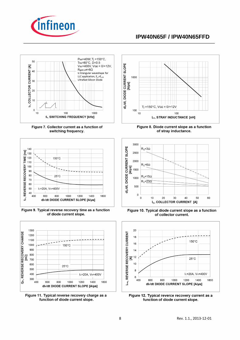
Diode reverse recovery time trr Tvj=25°C,
VR=400V,
IF=20.0A,
dIF/dt=1400 A/µs
- 55 - ns
Diode reverse recovery charge Qrr - 490 - nC
Diode peak reverse recovery current
Irr - 12.7 - A
Diode peak rate of fall of reverse recovery current during tb
dirr/dt - -1040 - A/µs
Thermal Resistance
Parameter Symbol Conditions Max. Value Unit
Characteristic IGBT thermal resistance, Rth(j-c) 0.60
K/W
junction – case
Diode thermal resistance, Rth(j-c) 1.80 junction - case
Thermal resistance, Rth(j-a) PG-TO247-3 40 junction – ambient
__________________________
1 RCE(eq) is computer at IC=Inom/2 and Vcesat at Inom/2.

IPW40N65F / IPW40N65FFD
7 Rev. 1.1., 2013-12-01
IPW40N65F / IPW40N65FFD
8 Rev. 1.1., 2013-12-01

IPW40N65F / IPW40N65FFD
9 Rev. 1.1., 2013-12-01

IPW40N65F / IPW40N65FFD
10 Rev. 1.1., 2013-12-01

IPW40N65F / IPW40N65FFD
11 Rev. 1.1., 2013-12-01
Revision History
IPW40N65F / IPW40N65FFD
Revision: 2013-12-01, Rev. 1.1
Previous Revision:
Revision Date Subjects (major changes since last revision)
1.1 2013-12-01 Preliminary datasheet
We Listen to Your Comments
Any information within this document that you feel is wrong, unclear or missing at all ? Your feedback will help us to continuously improve the quality of this document. Please send your proposal (including a reference to this document) to: [email protected] Published by Infineon Technologies AG 81726 Munich, Germany 81726 München, Germany © 2013 Infineon Technologies AG All Rights Reserved. Legal Disclaimer
The information given in this document shall in no event be regarded as a guarantee of conditions or characteristics. With respect to any examples or hints given herein, any typical values stated herein and/or any information regarding the application of the device, Infineon Technologies hereby disclaims any and all warranties and liabilities of any kind, including without limitation, warranties of non-infringement of intellectual property rights of any third party. Information
For further information on technology, delivery terms and conditions and prices, please contact the nearest Infineon Technologies Office (www.infineon.com). Warnings
Due to technical requirements, components may contain dangerous substances. For information on the types in question, please contact the nearest Infineon Technologies Office. The Infineon Technologies component described in this Data Sheet may be used in life-support devices or systems and/or automotive, aviation and aerospace applications or systems only with the express written approval of Infineon Technologies, if a failure of such components can reasonably be expected to cause the failure of that life-support, automotive, aviation and aerospace device or system or to affect the safety or effectiveness of that device or system. Life support devices or systems are intended to be implanted in the human body or to support and/or maintain and sustain and/or protect human life. If they fail, it is reasonable to assume that the health of the user or other persons may be endangered.
Mouser Electronics
Authorized Distributor
Click to View Pricing, Inventory, Delivery & Lifecycle Information: Infineon:
IPW40N65FFKSA1 IPW40N65FFDFKSA1