Embed Size (px)
Citation preview

1. Product profile
1.1 General descriptionThe IP4853CX24 is a device that fully integrates a bidirectional level shifter or voltage translator, ElectroMagnetic Interference (EMI) filter and ElectroStatic Discharge (ESD) protection diodes. It is specifically designed to be used for memory card interfaces such as Secure Digital (SD), microSD and Multi Media Card (MMC) memory cards.
The integrated Power Supply Unit (PSU) supplies memory cards with 2.9 V directly from the battery. This enables a 1.8 V operating host-side device (e.g. a processor interface) to communicate with a 2.9 V compliant memory card using its integrated level shifter. Radiation from digital signals in the higher harmonics, close to typical mobile phone frequencies, is suppressed by the EMI filter.
The IP4853CX24 is fabricated using monolithic silicon technology in a Wafer Level Chip-Size Package (WLCSP) with 0.4 mm pitch.
1.2 Features and benefitsPb-free, Restriction of Hazardous Substances (RoHS) compliant and free of halogen and antimony (Dark Green compliant)Integrated EMI filtersFeedback channel for clock synchronizationIntegrated ESD protection according to IEC 61000-4-2, level 4WLCSP with 0.4 mm pitch
1.3 ApplicationsSD-memory card, microSD-memory card and MMC interfaces in latest electronic appliances such as:
Mobile phone or smart phoneDigital cameraCard reader in (laptop) computer
Appliances requiring one or several of the following features:Level shifting and voltage translation from 1.8 V to 2.9 V and from 2.9 V to 1.8 VESD protection according to IEC 61000-4-2, level 4Power supply regulation from battery to 2.9 V card memory voltageEMI filteringIntegration of interface-specific biasing resistor network
IP4853CX24SD, MMC and microSD memory card integrated level shifter with PSU, EMI filter and ESD protectionRev. 3 — 30 September 2010 Product data sheet

NXP Semiconductors IP4853CX24SD, MMC and microSD memory card integrated level shifter
2. Pinning information
2.1 Pinning
2.2 Pin description
Fig 1. Pin configuration for WLCSP24 package
Table 1. Pin allocation tablePin Symbol Pin Symbol Pin Symbol Pin Symbol Pin SymbolA1 DATA2_H A2 DIR_CMD A3 DIR_0 A4 VBAT A5 DATA2_SD
B1 DATA3_H B2 n.c. B3 VCC B4 VSD B5 DATA3_SD
C1 CLK_IN C2 ENABLE C3 GND C4 GND C5 CLK_SD
D1 DATA0_H D2 CMD_H D3 CD D4 CMD_SD D5 DATA0_SD
E1 DATA1_H E2 CLK_FB E3 DIR_1_3 E4 WP E5 DATA1_SD
001aah951
IP4853CX24
Transparent top view
D
B
E
C
A
2 41 3 5
bump A1index area
Table 2. Pin descriptionSymbol[1] Pin Type[2] DescriptionDATA2_H A1 I/O data 2 input or output on host side
DIR_CMD A2 I direction control input for command
DIR_0 A3 I direction control input for data 0
VBAT A4 S supply voltage from battery for regulator
DATA2_SD A5 I/O data 2 input or output on memory card side
DATA3_H B1 I/O data 3 input or output on host side
n.c. B2 - not connected
VCC B3 S supply voltage for host-side circuits
VSD B4 O output supply voltage for memory card
DATA3_SD B5 I/O data 3 input or output on memory card side
CLK_IN C1 I clock signal input
IP4853CX24 All information provided in this document is subject to legal disclaimers. © NXP B.V. 2010. All rights reserved.
Product data sheet Rev. 3 — 30 September 2010 2 of 21

NXP Semiconductors IP4853CX24SD, MMC and microSD memory card integrated level shifter
[1] The pin names relate particularly to SD-memory cards, but also apply to microSD-memory cards and MMC.
[2] I = input, O = output, I/O = input and output, S = power supply.
3. Ordering information
ENABLE C2 I device enable input
GND C3 S supply ground
GND C4 S supply ground
CLK_SD C5 O clock signal output on memory card side
DATA0_H D1 I/O data 0 input or output on host side
CMD_H D2 I/O command input or output on host side
CD D3 O card detect switch biasing output
CMD_SD D4 I/O command input or output on memory card side
DATA0_SD D5 I/O data 0 input or output on memory card side
DATA1_H E1 I/O data 1 input or output on host side
CLK_FB E2 O clock feedback output to host
DIR_1_3 E3 I direction control input for data 1, data 2 and data 3
WP E4 O write protect switch biasing output
DATA1_SD E5 I/O data 1 input or output on memory card side
Table 2. Pin description …continued
Symbol[1] Pin Type[2] Description
Table 3. Ordering informationType number Package
Name Description VersionIP4853CX24/P WLCSP24 wafer level chip-size package; 24 bumps;
1.99 × 1.99 × 0.61 mmIP4853CX24/P
IP4853CX24 All information provided in this document is subject to legal disclaimers. © NXP B.V. 2010. All rights reserved.
Product data sheet Rev. 3 — 30 September 2010 3 of 21

NXP Semiconductors IP4853CX24SD, MMC and microSD memory card integrated level shifter
4. Block diagram
Fig 2. Block diagram
001aah980
CD
VOLTAGEREGULATOR
VBAT
CLK_IN
VSD
CLK_SD
CLK_FB
DIR_CMD
CMD_H
R13
R14
R7
R12
R11
R10
R1
R2
DIR_0
DATA0_H
CMD_SD
DATA0_SDR3
DIR_1_3
DATA1_H
R4
DATA2_H
DATA3_H
VCC
ENABLE
D3
C2
B3
B1
A1
E1
E3
D1
A3
E4
B5
A5
E5
D5
D4
C5
B4A4
C1
E2
A2
D2
C3, C4
DATA1_SD
DATA2_SD
host side SD card side
DATA3_SD
R5
R6
WP
R15GND
IP4853CX24
IP4853CX24 All information provided in this document is subject to legal disclaimers. © NXP B.V. 2010. All rights reserved.
Product data sheet Rev. 3 — 30 September 2010 4 of 21
NXP Semiconductors IP4853CX24SD, MMC and microSD memory card integrated level shifter
5. Functional description
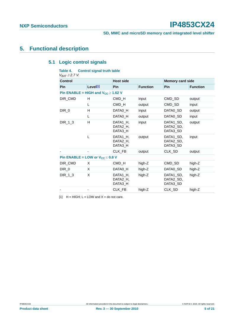
5.1 Logic control signals
[1] H = HIGH; L = LOW and X = do not care.
Table 4. Control signal truth tableVBAT ≥ 2.7 V.
Control Host side Memory card sidePin Level[1] Pin Function Pin FunctionPin ENABLE = HIGH and VCC ≥ 1.62 VDIR_CMD H CMD_H input CMD_SD output
L CMD_H output CMD_SD input
DIR_0 H DATA0_H input DATA0_SD output
L DATA0_H output DATA0_SD input
DIR_1_3 H DATA1_H, DATA2_H, DATA3_H
input DATA1_SD, DATA2_SD, DATA3_SD
output
L DATA1_H, DATA2_H, DATA3_H
output DATA1_SD, DATA2_SD, DATA3_SD
input
- - CLK_FB output CLK_SD output
Pin ENABLE = LOW or VCC ≤ 0.8 VDIR_CMD X CMD_H high-Z CMD_SD high-Z
DIR_0 X DATA0_H high-Z DATA0_SD high-Z
DIR_1_3 X DATA1_H, DATA2_H, DATA3_H
high-Z DATA1_SD, DATA2_SD, DATA3_SD
high-Z
- - CLK_FB high-Z CLK_SD high-Z
IP4853CX24 All information provided in this document is subject to legal disclaimers. © NXP B.V. 2010. All rights reserved.
Product data sheet Rev. 3 — 30 September 2010 5 of 21

NXP Semiconductors IP4853CX24SD, MMC and microSD memory card integrated level shifter
6. Limiting values
[1] Pin VBAT and all memory card-side pins to ground.
[2] All other pins to ground.
7. Recommended operating conditions
[1] The device is still fully functional, but the voltage on pin VSD might drop below the recommended memory card supply voltage.
Table 5. Limiting valuesIn accordance with the Absolute Maximum Rating System (IEC 60134). Voltages are referenced to GND (ground = 0 V).
Symbol Parameter Conditions Min Max UnitVCC supply voltage −0.5 +3.5 V
VBAT battery supply voltage 4 ms transient −0.5 +5.5 V
operating −0.5 +5.0 V
VI input voltage at I/O pins
4 ms transient −0.5 +5.5 V
operating −0.5 +5.0 V
Ptot total power dissipation Tamb = −30 °C to +70 °C - 550 mW
Tstg storage temperature −55 +150 °C
Tamb ambient temperature −30 +85 °C
VESD electrostatic discharge voltage
IEC 61000-4-2, level 4 [1]
contact - ±8 kV
air discharge - ±15 kV
IEC 61340-3-1, human body model
[2] - ±2 kV
Table 6. Operating conditionsSymbol Parameter Conditions Min Max UnitVCC supply voltage 1.62 2.1 V
VBAT battery supply voltage 2.7[1] 5.0 V
VI input voltage host side 0 2.1 V
memory card side; VBAT ≥ 3.2 V
0 2.9 V
VO output voltage active mode; pin ENABLE = HIGH
host side 0 VCC V
memory card side 0 VO(reg) V
Δt/ΔV time difference over voltage change
host side; VCC = 0.2 V to 0.7 V
- 2 ns/V
memory card side; VO(reg) = 0.2 V to 0.7 V
- 2 ns/V
IP4853CX24 All information provided in this document is subject to legal disclaimers. © NXP B.V. 2010. All rights reserved.
Product data sheet Rev. 3 — 30 September 2010 6 of 21

NXP Semiconductors IP4853CX24SD, MMC and microSD memory card integrated level shifter
8. Static characteristics
[1] Typical values are measured at Tamb = 25 °C.
[2] EMI filter line capacitance per data channel from I/O pin to driver; Cch is guaranteed by design.
Table 7. Static characteristicsAt recommended operating conditions; Tamb = −30 °C to +85 °C; voltages are referenced to GND (ground = 0 V); unless otherwise specified.
Symbol Parameter Conditions Min Typ[1] Max UnitVoltage regulator output: pin VSDVO(reg) regulator output voltage CL = 1 μF
IO(reg) = 0 A - 2.9 2.987 V
IO(reg) = 200 mA; VBAT ≥ 2.9 V 2.75 - - V
ΔVdo(reg) regulator dropout voltage variation
IO(reg) = 200 mA - - 150 mV
IO(reg) regulator output current - 200 - mA
IO(sc) short-circuit output current
- - 500 mA
Iq(reg) regulator quiescent current
pin ENABLE = HIGH (active mode) - - 200 μA
pin ENABLE = LOW (not active mode)
- - 2 μA
Cext external capacitance recommended capacitor at pin VSD - 1.0 - μF
Control and data inputsHost side: pins ENABLE, DIR_0, DIR_1_3, DIR_CMD, CLK_IN and DATA0_H to DATA3_H
VIH HIGH-level input voltage 0.65 × VCC - - V
VIL LOW-level input voltage - - 0.3 V
Cch channel capacitance VI = 0 V; fi = 1 MHz [2] - - 20 pF
Memory card side: pins CMD_SD and DATA0_SD to DATA3_SD
VIH HIGH-level input voltage 0.65 × VO(reg) - - V
VIL LOW-level input voltage - - 0.3 V
Cch channel capacitance VI = 0 V; fi = 1 MHz [2] - - 20 pF
Control and data outputsHost side: pins CLK_FB, CMD_H and DATA0_H to DATA3_H
VOH HIGH-level output voltage IO = −3 mA; VI = VIH VCC − 0.45 - - V
VOL LOW-level output voltage IO = 3 mA; VI = VIL - - 0.45 V
Memory card side: pins CLK_SD, CMD_SD and DATA0_SD to DATA3_SD, CD and WP
VOH HIGH-level output voltage IO = −6 mA; VI = VIH VO(reg) − 0.45 - - V
VOL LOW-level output voltage IO = 6 mA; VI = VIL - - 0.45 V
ILRzd Zener diode reverse leakage current
VI = 3 V - - 100 nA
Rs series resistance R1 to R6; tolerance ±20 % 32 40 48 Ω
Rpd pull-down resistance R7; tolerance ±30 % 329 470 611 kΩ
Rpu pull-up resistance R10; tolerance ±30 % 10.5 15 19.5 kΩ
R11 to R13; tolerance ±30 % 49 70 91 kΩ
R14 and R15; tolerance ±30 % 70 100 130 kΩ
IP4853CX24 All information provided in this document is subject to legal disclaimers. © NXP B.V. 2010. All rights reserved.
Product data sheet Rev. 3 — 30 September 2010 7 of 21

NXP Semiconductors IP4853CX24SD, MMC and microSD memory card integrated level shifter
9. Dynamic characteristics
[1] Guaranteed by design.
Table 8. Voltage regulatorTamb = 25 °C; unless otherwise specified.
Symbol Parameter Conditions Min Typ Max UnitVoltage regulator output: pin VSDPSRR power supply
rejection ratioVBAT = 3.0 V; Vripple(p-p) = 223.6 mV (0 dBm); Rsource = 50 Ω
fripple = 1 kHz 40 - - dB
fripple = 10 kHz 30 - - dB
tstartup(reg) regulator start-up time
VCC = 1.8 V; VBAT = 3.0 V; IO(reg) = 200 mA; CL = 1 μF; see Figure 3
- - 200 μs
Measuring points: ENABLE signal at 0.5VCC and regulator output signal at 0.97VO(reg).
Fig 3. Regulator start-up time
Table 9. Frequency response of integrated EMI filtersTamb = 25 °C; unless otherwise specified.
Symbol Parameter Conditions Min Typ Max UnitClock, command and data channels[1]
αil insertion loss Rsource = 50 Ω; CL = 10 pF; RL = 50 Ω
fi = 401 MHz to 800 MHz 9 - - dB
fi = 801 MHz to 1.4 GHz - 17 - dB
fi = 1.4 GHz to 6.0 GHz - 32 - dB
001aah981
VI
GND
97 %
50 %
tstartup(reg)
VO(reg)
regulatoroutput
ENABLE
0 V
IP4853CX24 All information provided in this document is subject to legal disclaimers. © NXP B.V. 2010. All rights reserved.
Product data sheet Rev. 3 — 30 September 2010 8 of 21
NXP Semiconductors IP4853CX24SD, MMC and microSD memory card integrated level shifter
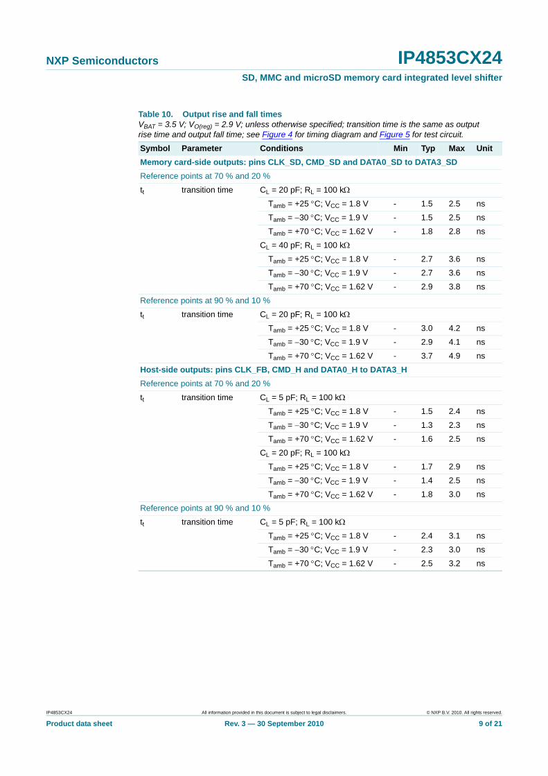
Table 10. Output rise and fall timesVBAT = 3.5 V; VO(reg) = 2.9 V; unless otherwise specified; transition time is the same as output rise time and output fall time; see Figure 4 for timing diagram and Figure 5 for test circuit.
Symbol Parameter Conditions Min Typ Max UnitMemory card-side outputs: pins CLK_SD, CMD_SD and DATA0_SD to DATA3_SDReference points at 70 % and 20 %
tt transition time CL = 20 pF; RL = 100 kΩ
Tamb = +25 °C; VCC = 1.8 V - 1.5 2.5 ns
Tamb = −30 °C; VCC = 1.9 V - 1.5 2.5 ns
Tamb = +70 °C; VCC = 1.62 V - 1.8 2.8 ns
CL = 40 pF; RL = 100 kΩ
Tamb = +25 °C; VCC = 1.8 V - 2.7 3.6 ns
Tamb = −30 °C; VCC = 1.9 V - 2.7 3.6 ns
Tamb = +70 °C; VCC = 1.62 V - 2.9 3.8 ns
Reference points at 90 % and 10 %
tt transition time CL = 20 pF; RL = 100 kΩ
Tamb = +25 °C; VCC = 1.8 V - 3.0 4.2 ns
Tamb = −30 °C; VCC = 1.9 V - 2.9 4.1 ns
Tamb = +70 °C; VCC = 1.62 V - 3.7 4.9 ns
Host-side outputs: pins CLK_FB, CMD_H and DATA0_H to DATA3_HReference points at 70 % and 20 %
tt transition time CL = 5 pF; RL = 100 kΩ
Tamb = +25 °C; VCC = 1.8 V - 1.5 2.4 ns
Tamb = −30 °C; VCC = 1.9 V - 1.3 2.3 ns
Tamb = +70 °C; VCC = 1.62 V - 1.6 2.5 ns
CL = 20 pF; RL = 100 kΩ
Tamb = +25 °C; VCC = 1.8 V - 1.7 2.9 ns
Tamb = −30 °C; VCC = 1.9 V - 1.4 2.5 ns
Tamb = +70 °C; VCC = 1.62 V - 1.8 3.0 ns
Reference points at 90 % and 10 %
tt transition time CL = 5 pF; RL = 100 kΩ
Tamb = +25 °C; VCC = 1.8 V - 2.4 3.1 ns
Tamb = −30 °C; VCC = 1.9 V - 2.3 3.0 ns
Tamb = +70 °C; VCC = 1.62 V - 2.5 3.2 ns
IP4853CX24 All information provided in this document is subject to legal disclaimers. © NXP B.V. 2010. All rights reserved.
Product data sheet Rev. 3 — 30 September 2010 9 of 21

NXP Semiconductors IP4853CX24SD, MMC and microSD memory card integrated level shifter
[1] tPD is the same as HIGH-to-LOW propagation delay (tPHL) and LOW-to-HIGH propagation delay (tPLH).
Table 11. Propagation delay of time domain response driver partVBAT = 3.5 V; VO(reg) = 2.9 V; Rsource = 50 Ω; propagation delay measurements include PCB delays and connectors; see Figure 4 for timing diagram and Figure 5 for test circuit.
Symbol Parameter Conditions Min Typ Max UnitHost-side inputs to memory card-side outputstPD propagation delay nominal case; Tamb = +27 °C;
VCC = 1.8 V[1]
CL = 20 pF 6.2 7.0 7.8 ns
CL = 40 pF 7.3 8.2 9.1 ns
best case; Tamb = −30 °C; VCC = 1.9 V
CL = 20 pF 5.7 6.5 7.3 ns
CL = 40 pF 6.5 7.5 8.5 ns
worst case; Tamb = +70 °C; VCC = 1.62 V
CL = 20 pF 6.7 7.8 8.9 ns
CL = 40 pF 7.5 8.8 10.1 ns
Memory card-side inputs to host-side outputstPD propagation delay nominal case; Tamb = +27 °C;
VCC = 1.8 V[1]
CL = 5 pF 4.2 6.0 7.8 ns
CL = 20 pF 6.3 7.2 8.1 ns
best case; Tamb = −30 °C; VCC = 1.9 V
CL = 5 pF 4 5.9 6.9 ns
CL = 20 pF 5.1 6.7 8.5 ns
worst case; Tamb = +70 °C; VCC = 1.62 V
CL = 5 pF 5.4 6.5 7.7 ns
CL = 20 pF 6.7 8.0 9.2 ns
Host-side pins CLK_IN to CLK_FBtPD propagation delay nominal case; Tamb = +27 °C;
VCC = 1.8 V[1]
CL = 5 pF 7.6 9.2 10.7 ns
CL = 20 pF 8.2 9.9 11.6 ns
best case; Tamb = −30 °C; VCC = 1.9 V
CL = 5 pF 6.7 8.1 9.5 ns
CL = 20 pF 7.6 8.8 10.5 ns
worst case; Tamb = +70 °C; VCC = 1.62 V
CL = 5 pF 8.5 10.7 12.9 ns
CL = 20 pF 9.1 11.4 13.9 ns
IP4853CX24 All information provided in this document is subject to legal disclaimers. © NXP B.V. 2010. All rights reserved.
Product data sheet Rev. 3 — 30 September 2010 10 of 21

NXP Semiconductors IP4853CX24SD, MMC and microSD memory card integrated level shifter
[1] Power consumption is largely dependent on capacitive load connected to a driver output: P = VCC × ICC + VBAT × IBAT.
Measuring points: host side at 0.5VCC and memory card side at 0.5VO(reg).VOL and VOH are typical output voltage levels that occur with the output load.
Fig 4. Output rise and fall times and data input to output propagation delay times (host side to card side or card side to host side)
Table 12. Power dissipation per channelVCC = 1.8 V; VBAT = 4 V; all values are typical; memory card side CL = 20 pF and host side CL = 5 pF.
Frequency (MHz) IBAT (mA) ICC (mA) P (mW)[1]
Host-side input to memory card-side outputData channel
1.0 0.79 0.002 3.16
10.0 3.30 0.020 13.3
20.0 5.79 0.037 23.2
50.0 12.3 0.090 49.4
Clock channel
1.0 0.44 0.05 1.85
10.0 3.1 0.59 13.5
20.0 5.4 0.97 23.4
50.0 12.2 2.36 53.1
Memory card-side input to host-side outputData channel
1.0 0.18 0.1 0.9
10.0 0.42 0.96 3.41
20.0 0.66 1.91 6.1
50.0 1.4 4.5 13.7
001aae967
A, B input
B, A output
tPLHtPHL
GND
VI
VOH
VM
VM
VOL
IP4853CX24 All information provided in this document is subject to legal disclaimers. © NXP B.V. 2010. All rights reserved.
Product data sheet Rev. 3 — 30 September 2010 11 of 21

NXP Semiconductors IP4853CX24SD, MMC and microSD memory card integrated level shifter
10. Test information
11. Marking
Definitions test circuit:Rsource = source resistance of pulse generator.Rterm = termination resistance should be equal to output impedance Z0 of the pulse generator.CL = load capacitance including jig and probe capacitance.RL = load resistance.
Fig 5. Load circuitry for measuring switching time
50 % 50 %
tW
tW
20 %
70 %
0 V
VI
VI
negativeinput
positiveinput
0 V
50 % 50 %
70 %
20 %
tf
tr
tr
tf
001aah982
DUT
VCCVBAT
VI VO
Rterm
Rsource
RLCL
PULSEGENERATORtr = tf = 1.8 ns
DUT50 Ω
Fig 6. Marking of IP4853CX24
018aaa000
top view
bump A1indicator
LASER MARKINGAREA
IP4853CX24 All information provided in this document is subject to legal disclaimers. © NXP B.V. 2010. All rights reserved.
Product data sheet Rev. 3 — 30 September 2010 12 of 21

NXP Semiconductors IP4853CX24SD, MMC and microSD memory card integrated level shifter
12. Package outline
Fig 7. Package outline IP4853CX24 (WLCSP24)
wlcsp24_5x5-b2_po
Europeanprojection
WLCSP24: wafer level chip-size package; 24 bumps (5 x 5 - B2)
bump A1index area
D
E
X
detail X
A
A2
A1
b
A
B
C
D
E
2 41 3 5
e1
e1
e
e
Table 13. Package outline dimensionsSymbol Min Typ Max UnitA 0.57 0.61 0.65 mm
A1 0.18 0.20 0.22 mm
A2 0.39 0.41 0.43 mm
b 0.21 0.26 0.31 mm
D 1.94 1.99 2.04 mm
E 1.94 1.99 2.04 mm
e - 0.40 - mm
e1 - 1.6 - mm
IP4853CX24 All information provided in this document is subject to legal disclaimers. © NXP B.V. 2010. All rights reserved.
Product data sheet Rev. 3 — 30 September 2010 13 of 21

NXP Semiconductors IP4853CX24SD, MMC and microSD memory card integrated level shifter
13. Packing information
Fig 8. Tape and reel information
001aai051
B - B
K
A - A
B0
T1
G
T
K0A0
P2
P0
D0
W1
P
WF
E
D1
θ
A
BB
A 0.05 / 40
direction of feed
position of PIN A1
Table 14. Tape dimensionsDescription Item Symbol Specification (mm)
Dimension ToleranceOverall dimensions tape width W 8.00 ±0.1
thickness K 1.20 max.
distance G 0.75 min.
Sprocket holes[1] diameter D0 1.50 +0.1
distance E 1.75 ±0.1
pitch P0 4.00 ±0.1
Distance between center lines length direction P2 2.00 ±0.05
width direction F 3.50 ±0.05
Compartments length A0 2.20 ±0.05
width B0 2.20 ±0.05
depth K0 0.80 ±0.05
hole diameter D1 0.50 +0.1
pitch P 4.00 ±0.1
IP4853CX24 All information provided in this document is subject to legal disclaimers. © NXP B.V. 2010. All rights reserved.
Product data sheet Rev. 3 — 30 September 2010 14 of 21

NXP Semiconductors IP4853CX24SD, MMC and microSD memory card integrated level shifter
[1] Cumulated pitch error: ±0.2 mm per 10 pitches.
[2] Carbon loaded polystyrene 100 % recyclable.
[3] The cover tape shall not overlap the sprocket holes.
14. Design and assembly recommendations
14.1 PCB design guidelinesTo achieve optimum performance it is recommended to use a Non-Solder Mask Design (NSMD) Printed-Circuit Board (PCB) design, also known as a copper-defined design, incorporating laser-drilled micro-vias connecting the ground pads to a buried ground-plane layer. This results in the lowest possible ground inductance and provides the best high frequency and ESD performance. Refer to Table 15 for the recommended PCB design parameters.
14.2 PCB assembly guidelines for Pb-free soldering
[1] 3 to 4.
[2] 0.5 to 0.9.
Device rotation θ 20° max.
Carrier tape antistatic[2] film thickness T 0.25 ±0.07
Cover tape[3] width W1 5.75 max.
film thickness T1 0.1 max.
Bending radius in winding direction R 30 min.
Table 14. Tape dimensions …continued
Description Item Symbol Specification (mm)Dimension Tolerance
Table 15. Recommended PCB design parametersPCB pad size 225 μm diameter
Micro-via diameter 100 μm
Solder mask opening 335 μm diameter
Copper thickness 20 μm to 40 μm
Copper finish OSP
PCB material FR4
Table 16. Assemble recommendationsSolder screen aperture size 255 μm diameter
Solder screen thickness 100 μm (0.004")
Solder paste: Pb-free SnAg[1]Cu[2]
Solder/flux ratio 50 : 50
Solder reflow profile see Figure 9
IP4853CX24 All information provided in this document is subject to legal disclaimers. © NXP B.V. 2010. All rights reserved.
Product data sheet Rev. 3 — 30 September 2010 15 of 21
NXP Semiconductors IP4853CX24SD, MMC and microSD memory card integrated level shifter
The device is capable of withstanding at least three reflows of this profile.
Fig 9. Pb-free solder reflow profile
Table 17. CharacteristicsSymbol Parameter Conditions Min Typ Max UnitTreflow(peak) peak reflow temperature 230 - 260 °C
t1 time 1 soak time 60 - 180 s
t2 time 2 time from T = 25 °C to Treflow(peak)
240 - 300 s
t3 time 3 time during T ≥ 250 °C - - 30 s
t4 time 4 time during T ≥ 230 °C 10 - 50 s
t5 time 5 time during T > 217 °C 30 - 150 s
dT/dt rate of change of temperature
cooling rate - - −6 °C/s
pre-heat 2.5 - 4.0 °C/s
001aai161
Treflow(peak)250
230
217
T(°C)
cooling rate
pre-heat
t1t2
t5
t4
t3t (s)
IP4853CX24 All information provided in this document is subject to legal disclaimers. © NXP B.V. 2010. All rights reserved.
Product data sheet Rev. 3 — 30 September 2010 16 of 21

NXP Semiconductors IP4853CX24SD, MMC and microSD memory card integrated level shifter
15. Abbreviations
Table 18. AbbreviationsAcronym DescriptionDUT Device Under Test
EMI ElectroMagnetic Interference
ESD ElectroStatic Discharge
FR4 Flame Retard 4
MMC Multi Media Card
NSMD Non-Solder Mask Design
OSP Organic Solderability Preservation
PCB Printed-Circuit Board
PSU Power Supply Unit
RoHS Restriction of Hazardous Substances
SD Secure Digital
WLCSP Wafer Level Chip-Size Package
IP4853CX24 All information provided in this document is subject to legal disclaimers. © NXP B.V. 2010. All rights reserved.
Product data sheet Rev. 3 — 30 September 2010 17 of 21
NXP Semiconductors IP4853CX24SD, MMC and microSD memory card integrated level shifter
16. Revision history
Table 19. Revision historyDocument ID Release date Data sheet status Change notice SupersedesIP4853CX24 v.3 20100930 Product data sheet - IP4853CX24_2
Modifications: • Section 3 “Ordering information”: updated.• Figure 6 “Marking of IP4853CX24”: updated.• Section 12 “Package outline”: updated.• Figure 8 “Tape and reel information”: updated.• Table 17: Treflow(peak) updated.• Section 17 “Legal information”: updated.
IP4853CX24_2 20090615 Product data sheet - IP4853CX24_1
IP4853CX24_1 20080722 Product data sheet - -
IP4853CX24 All information provided in this document is subject to legal disclaimers. © NXP B.V. 2010. All rights reserved.
Product data sheet Rev. 3 — 30 September 2010 18 of 21
NXP Semiconductors IP4853CX24SD, MMC and microSD memory card integrated level shifter
17. Legal information
17.1 Data sheet status
[1] Please consult the most recently issued document before initiating or completing a design.
[2] The term ‘short data sheet’ is explained in section “Definitions”.
[3] The product status of device(s) described in this document may have changed since this document was published and may differ in case of multiple devices. The latest product status information is available on the Internet at URL http://www.nxp.com.
17.2 DefinitionsDraft — The document is a draft version only. The content is still under internal review and subject to formal approval, which may result in modifications or additions. NXP Semiconductors does not give any representations or warranties as to the accuracy or completeness of information included herein and shall have no liability for the consequences of use of such information.
Short data sheet — A short data sheet is an extract from a full data sheet with the same product type number(s) and title. A short data sheet is intended for quick reference only and should not be relied upon to contain detailed and full information. For detailed and full information see the relevant full data sheet, which is available on request via the local NXP Semiconductors sales office. In case of any inconsistency or conflict with the short data sheet, the full data sheet shall prevail.
Product specification — The information and data provided in a Product data sheet shall define the specification of the product as agreed between NXP Semiconductors and its customer, unless NXP Semiconductors and customer have explicitly agreed otherwise in writing. In no event however, shall an agreement be valid in which the NXP Semiconductors product is deemed to offer functions and qualities beyond those described in the Product data sheet.
17.3 DisclaimersLimited warranty and liability — Information in this document is believed to be accurate and reliable. However, NXP Semiconductors does not give any representations or warranties, expressed or implied, as to the accuracy or completeness of such information and shall have no liability for the consequences of use of such information.
In no event shall NXP Semiconductors be liable for any indirect, incidental, punitive, special or consequential damages (including - without limitation - lost profits, lost savings, business interruption, costs related to the removal or replacement of any products or rework charges) whether or not such damages are based on tort (including negligence), warranty, breach of contract or any other legal theory.
Notwithstanding any damages that customer might incur for any reason whatsoever, NXP Semiconductors’ aggregate and cumulative liability towards customer for the products described herein shall be limited in accordance with the Terms and conditions of commercial sale of NXP Semiconductors.
Right to make changes — NXP Semiconductors reserves the right to make changes to information published in this document, including without limitation specifications and product descriptions, at any time and without notice. This document supersedes and replaces all information supplied prior to the publication hereof.
Suitability for use — NXP Semiconductors products are not designed, authorized or warranted to be suitable for use in life support, life-critical or safety-critical systems or equipment, nor in applications where failure or
malfunction of an NXP Semiconductors product can reasonably be expected to result in personal injury, death or severe property or environmental damage. NXP Semiconductors accepts no liability for inclusion and/or use of NXP Semiconductors products in such equipment or applications and therefore such inclusion and/or use is at the customer’s own risk.
Applications — Applications that are described herein for any of these products are for illustrative purposes only. NXP Semiconductors makes no representation or warranty that such applications will be suitable for the specified use without further testing or modification.
Customers are responsible for the design and operation of their applications and products using NXP Semiconductors products, and NXP Semiconductors accepts no liability for any assistance with applications or customer product design. It is customer’s sole responsibility to determine whether the NXP Semiconductors product is suitable and fit for the customer’s applications and products planned, as well as for the planned application and use of customer’s third party customer(s). Customers should provide appropriate design and operating safeguards to minimize the risks associated with their applications and products.
NXP Semiconductors does not accept any liability related to any default, damage, costs or problem which is based on any weakness or default in the customer’s applications or products, or the application or use by customer’s third party customer(s). Customer is responsible for doing all necessary testing for the customer’s applications and products using NXP Semiconductors products in order to avoid a default of the applications and the products or of the application or use by customer’s third party customer(s). NXP does not accept any liability in this respect.
Limiting values — Stress above one or more limiting values (as defined in the Absolute Maximum Ratings System of IEC 60134) will cause permanent damage to the device. Limiting values are stress ratings only and (proper) operation of the device at these or any other conditions above those given in the Recommended operating conditions section (if present) or the Characteristics sections of this document is not warranted. Constant or repeated exposure to limiting values will permanently and irreversibly affect the quality and reliability of the device.
Terms and conditions of commercial sale — NXP Semiconductors products are sold subject to the general terms and conditions of commercial sale, as published at http://www.nxp.com/profile/terms, unless otherwise agreed in a valid written individual agreement. In case an individual agreement is concluded only the terms and conditions of the respective agreement shall apply. NXP Semiconductors hereby expressly objects to applying the customer’s general terms and conditions with regard to the purchase of NXP Semiconductors products by customer.
No offer to sell or license — Nothing in this document may be interpreted or construed as an offer to sell products that is open for acceptance or the grant, conveyance or implication of any license under any copyrights, patents or other industrial or intellectual property rights.
Export control — This document as well as the item(s) described herein may be subject to export control regulations. Export might require a prior authorization from national authorities.
Document status[1][2] Product status[3] Definition
Objective [short] data sheet Development This document contains data from the objective specification for product development.
Preliminary [short] data sheet Qualification This document contains data from the preliminary specification.
Product [short] data sheet Production This document contains the product specification.
IP4853CX24 All information provided in this document is subject to legal disclaimers. © NXP B.V. 2010. All rights reserved.
Product data sheet Rev. 3 — 30 September 2010 19 of 21

NXP Semiconductors IP4853CX24SD, MMC and microSD memory card integrated level shifter
Non-automotive qualified products — Unless this data sheet expressly states that this specific NXP Semiconductors product is automotive qualified, the product is not suitable for automotive use. It is neither qualified nor tested in accordance with automotive testing or application requirements. NXP Semiconductors accepts no liability for inclusion and/or use of non-automotive qualified products in automotive equipment or applications.
In the event that customer uses the product for design-in and use in automotive applications to automotive specifications and standards, customer (a) shall use the product without NXP Semiconductors’ warranty of the product for such automotive applications, use and specifications, and (b) whenever customer uses the product for automotive applications beyond
NXP Semiconductors’ specifications such use shall be solely at customer’s own risk, and (c) customer fully indemnifies NXP Semiconductors for any liability, damages or failed product claims resulting from customer design and use of the product for automotive applications beyond NXP Semiconductors’ standard warranty and NXP Semiconductors’ product specifications.
17.4 TrademarksNotice: All referenced brands, product names, service names and trademarks are the property of their respective owners.
18. Contact information
For more information, please visit: http://www.nxp.com
For sales office addresses, please send an email to: [email protected]
IP4853CX24 All information provided in this document is subject to legal disclaimers. © NXP B.V. 2010. All rights reserved.
Product data sheet Rev. 3 — 30 September 2010 20 of 21

NXP Semiconductors IP4853CX24SD, MMC and microSD memory card integrated level shifter
19. Contents
1 Product profile . . . . . . . . . . . . . . . . . . . . . . . . . . 11.1 General description . . . . . . . . . . . . . . . . . . . . . 11.2 Features and benefits . . . . . . . . . . . . . . . . . . . . 11.3 Applications . . . . . . . . . . . . . . . . . . . . . . . . . . . 12 Pinning information. . . . . . . . . . . . . . . . . . . . . . 22.1 Pinning . . . . . . . . . . . . . . . . . . . . . . . . . . . . . . . 22.2 Pin description . . . . . . . . . . . . . . . . . . . . . . . . . 23 Ordering information. . . . . . . . . . . . . . . . . . . . . 34 Block diagram . . . . . . . . . . . . . . . . . . . . . . . . . . 45 Functional description . . . . . . . . . . . . . . . . . . . 55.1 Logic control signals . . . . . . . . . . . . . . . . . . . . . 56 Limiting values. . . . . . . . . . . . . . . . . . . . . . . . . . 67 Recommended operating conditions. . . . . . . . 68 Static characteristics. . . . . . . . . . . . . . . . . . . . . 79 Dynamic characteristics . . . . . . . . . . . . . . . . . . 810 Test information. . . . . . . . . . . . . . . . . . . . . . . . 1211 Marking . . . . . . . . . . . . . . . . . . . . . . . . . . . . . . . 1212 Package outline . . . . . . . . . . . . . . . . . . . . . . . . 1313 Packing information . . . . . . . . . . . . . . . . . . . . 1414 Design and assembly recommendations . . . 1514.1 PCB design guidelines . . . . . . . . . . . . . . . . . . 1514.2 PCB assembly guidelines for Pb-free
soldering . . . . . . . . . . . . . . . . . . . . . . . . . . . . . 1515 Abbreviations. . . . . . . . . . . . . . . . . . . . . . . . . . 1716 Revision history. . . . . . . . . . . . . . . . . . . . . . . . 1817 Legal information. . . . . . . . . . . . . . . . . . . . . . . 1917.1 Data sheet status . . . . . . . . . . . . . . . . . . . . . . 1917.2 Definitions. . . . . . . . . . . . . . . . . . . . . . . . . . . . 1917.3 Disclaimers . . . . . . . . . . . . . . . . . . . . . . . . . . . 1917.4 Trademarks. . . . . . . . . . . . . . . . . . . . . . . . . . . 2018 Contact information. . . . . . . . . . . . . . . . . . . . . 2019 Contents . . . . . . . . . . . . . . . . . . . . . . . . . . . . . . 21
© NXP B.V. 2010. All rights reserved.For more information, please visit: http://www.nxp.comFor sales office addresses, please send an email to: [email protected]
Date of release: 30 September 2010Document identifier: IP4853CX24
Please be aware that important notices concerning this document and the product(s)described herein, have been included in section ‘Legal information’.


![(e)MMC/SD/SDIO State of Affairsconnect.linaro.org.s3.amazonaws.com/sfo17... · First MMC stack by Russell King in kernel 2.6.9 [MMC] Add MMC core](https://img.dokumen.tips/doc/110x75/5f5ee69463a1e67f0c5f43dc/emmcsdsdio-state-of-first-mmc-stack-by-russell-king-in-kernel-269-mmc-add.jpg)


![microSD-CONF 1 タヴシクヴダ · 2011-08-08 · 1 or 8 bit幅 エリア設定 ロータリSW ①microSD => FPGA直接転送モード microSD microSD-CONF1 XMODE XAREA[3:0] 図1-1.uSD-CONF1](https://img.dokumen.tips/doc/110x75/5f30bf189d8acd0cba350893/microsd-conf-1-fff-2011-08-08-1-or-8-bit-iiie-iiiisw.jpg)


