Embed Size (px)
Citation preview

I/O Planning Tutorial
PlanAhead Design Tool
UG674 (v 14.5) April 10, 2013
This tutorial document was last validated using the following software version: ISE Design Suite 14.5This tutorial document was last validated using the following software version: ISE Design Suite 14.5This tutorial document was last validated using the following software version: ISE Design Suite 14.5This tutorial document was last validated using the following software version: ISE Design Suite 14.5
If using a later software version, there may be minor differences between the images and results shown inIf using a later software version, there may be minor differences between the images and results shown inIf using a later software version, there may be minor differences between the images and results shown inIf using a later software version, there may be minor differences between the images and results shown inthis document with what you will see in the Design Suite.this document with what you will see in the Design Suite.this document with what you will see in the Design Suite.this document with what you will see in the Design Suite.
I/O Planning Tutorial www.xilinx.com 2
UG674 (v 14.5) April 10, 2013
Notice of Disclaimer
The information disclosed to you hereunder (the "Materials") is provided solely for the selection and use of Xilinx products. To the
maximum extent permitted by applicable law: (1) Materials are made available "AS IS" and with all faults, Xilinx hereby DISCLAIMS ALL
WARRANTIES AND CONDITIONS, EXPRESS, IMPLIED, OR STATUTORY, INCLUDING BUT NOT LIMITED TO WARRANTIES OF
MERCHANTABILITY, NON-INFRINGEMENT, OR FITNESS FOR ANY PARTICULAR PURPOSE; and (2) Xilinx shall not be liable (whether in
contract or tort, including negligence, or under any other theory of liability) for any loss or damage of any kind or nature related to,
arising under, or in connection with, the Materials (including your use of the Materials), including for any direct, indirect, special,
incidental, or consequential loss or damage (including loss of data, profits, goodwill, or any type of loss or damage suffered as a result of
any action brought by a third party) even if such damage or loss was reasonably foreseeable or Xilinx had been advised of the possibility
of the same. Xilinx assumes no obligation to correct any errors contained in the Materials or to notify you of updates to the Materials or
to product specifications. You may not reproduce, modify, distribute, or publicly display the Materials without prior written consent.
Certain products are subject to the terms and conditions of the Limited Warranties which can be viewed at
http://www.xilinx.com/warranty.htm; IP cores may be subject to warranty and support terms contained in a license issued to you
by Xilinx. Xilinx products are not designed or intended to be fail-safe or for use in any application requiring fail-safe performance; you
assume sole risk and liability for use of Xilinx products in Critical Applications: http://www.xilinx.com/warranty.htm#critapps.
©Copyright 2010-2013 Xilinx, Inc. Xilinx, the Xilinx logo, Artix, ISE, Kintex, Spartan, Virtex, Vivado, Zynq, and other designated brands
included herein are trademarks of Xilinx in the United States and other countries. All other trademarks are the property of their respective
owners.
Revision History
Date Version Revision
04/10/2013 14.5 Validated with Release.

I/O Planning Tutorial www.xilinx.com 3
UG674 (v 14.5) April 10, 2013
Table of Contents
Revision History........................................................................................................................................................... 2
Table of Contents ................................................................................................................................................................................. 3
I/O Planning Tutorial ........................................................................................................................................................................... 5
Introduction .................................................................................................................................................................. 5
Tutorial Design Description .................................................................................................................................... 6
Software Requirements ............................................................................................................................................ 6
Hardware Requirements .......................................................................................................................................... 6
Preparing the Tutorial Design Files ...................................................................................................................... 6
Lab 1: Using I/O Planning Projects ................................................................................................................................................ 7
Step 1: Creating a New Project ............................................................................................................................. 7
Step 2: Examining Device I/O Resources ........................................................................................................ 11
Examining I/O Banks .......................................................................................................................................... 11
Step 3: Prohibiting Pins from I/O Assignment ............................................................................................. 14
Step 4: Creating and Configuring I/O Ports .................................................................................................. 15
Step 5: Importing an I/O Port List ..................................................................................................................... 16
Importing and Examining the CSV Format I/O Port List ...................................................................... 16
Step 6: Exporting the Device and I/O Pin Assignments ............................................................................ 18
Step 7: Migrating the I/O Planning Project to an RTL Project ................................................................ 18
Closing the RTL Project ..................................................................................................................................... 20
Lab 2: I/O Planning in a Synthesized Design .......................................................................................................................... 21
Step 1: Opening the Netlist-Based Project .................................................................................................... 21
Step 2: Examining the I/O Ports in the Design ............................................................................................. 22
Step 3: Configuring I/O Ports .............................................................................................................................. 23
Step 4: Creating I/O Port Interfaces.................................................................................................................. 24
Step 5: Viewing Multi-function Pins ................................................................................................................. 26
Step 6: Setting Device Configuration Modes ................................................................................................ 27
Step 7: Defining Alternate Compatible Devices ........................................................................................... 28
Send Feedback

I/O Planning Tutorial www.xilinx.com 4
UG674 (v 14.5) April 10, 2013
Step 8: Placing I/O Ports ....................................................................................................................................... 29
Placing I/O Ports in an I/O Bank .................................................................................................................... 29
Placing I/O Ports in an Area ............................................................................................................................ 30
Placing I/O Ports Sequentially ........................................................................................................................ 31
Step 9: Placing Clock Logic .................................................................................................................................. 32
Step 10: Using the Schematic to Trace Clock Logic ................................................................................... 33
Step 11: Exploring the Clock Resources View ............................................................................................... 35
Step 12: Placing the MCM Instance .................................................................................................................. 37
Step 13: Running Design Rule Checks ............................................................................................................. 38
Step 14: Running Simultaneous Switching Noise Analysis ...................................................................... 39
Step 15: Saving the Constraint Files ................................................................................................................. 40
Close the PlanAhead Tool ................................................................................................................................ 41
Conclusion .................................................................................................................................................................. 41
Send Feedback
I/O Planning Tutorial www.xilinx.com 5
UG674 (v 14.5) April 10, 2013
I/O Planning Tutorial
Introduction
This tutorial introduces the Xilinx® PlanAhead™ software capabilities for performing I/O port
assignment for FPGA devices. It describes the procedure for creating I/O ports and assigning
them to physical package pins. The I/O Planning view environment enables you to create,
import, and configure the initial list of I/O ports. You can group the related ports into Interfaces
and then assign them to package pins.
The objective of this tutorial is to familiarize you with the I/O pin planning process using the I/O
Planning functionality in the PlanAhead tool. There are two parts to this tutorial that can be
performed independently. The first part briefly describes I/O planning capabilities prior to
having a synthesized netlist or RTL Sources with I/O ports defined. The second part describes
I/O planning functionality after synthesis. Most of the PlanAhead I/O planning features are
described in Part2. However, many of them are available prior to running synthesis as well.
The capabilities include semi-automated modes for controlled I/O port assignment. Fully
automatic pin placement is also available for some device architectures. The I/O Planning view
environment shows the relationship of the physical package pins and I/O banks with their
corresponding die pads.
You can perform I/O pin assignment at various stages of the design cycle. You can perform I/O
exploration and assignment with an I/O Planning project even before the design source files are
available. You can import a Comma Separated Value (CSV) format file for I/O planning, or export
it for use in PCB schematic symbol or Hardware Description Language (HDL) header generation.
The PlanAhead tool also enables you to I/O pin plan in the elaborated Register Transfer Level
(RTL) design or in the synthesized netlist design. The PlanAhead tool performs more
comprehensive I/O and clocking DRCs when using a netlist design.
Not all commands or command options are covered in this tutorial. This tutorial uses the
features contained in the PlanAhead tool, which is bundled as a part of ISE® Design Suite
version 14.5.
Send Feedback

I/O Planning Tutorial www.xilinx.com 6
UG674 (v 14.5) April 10, 2013
Tutorial Design Description
The design targets an xc7k70t device The small sample design used in this tutorial includes:
A RISC processor CPU core
A pseudo FFT
Four gigabit transceivers (GTs)
Two USB interfaces
Software Requirements
The PlanAhead tool is installed with ISE Design Suite software. Before starting the tutorial, be
sure that the PlanAhead tool is operational, and that the tutorial design data is installed.
For installation instructions and information, see the ISE Design Suite 14: Release Notes,
Installation, and Licensing (UG631).
Hardware Requirements
Xilinx recommends a minimum of 2 GB of RAM when using the PlanAhead tool on larger
devices.
For this tutorial, a smaller xc7k70t design is used, and the number of designs open at one time is
limited. Although 1 GB is sufficient, it can impact performance.
Preparing the Tutorial Design Files
Copy the files from the ISE software installation area:
<ISE_install_area>/ISE_DS/PlanAhead/examples/PlanAhead_Tutorial.zip
Extract the zip file contents into any write-accessible location which will be referred to in this
tutorial as the extraction directory, or <Extract_dir>.
RECOMMENDED: The tutorial sample design data is modified while performing this
tutorial. A new copy of the original PlanAhead_Tutorial data should be extracted
each time you run this tutorial.
Send Feedback

Step 1: Creating a New Project
I/O Planning Tutorial www.xilinx.com 7
UG674 (v 14.5) April 10, 2013
Lab 1: Using I/O Planning Projects
The PlanAhead tool provides an I/O Planning view layout that displays views more applicable to
placing I/O Ports and clock logic. You can open the I/O planning layout without a design to
analyze device resources.
These first few I/O Pin Planning steps involve pre-synthesis techniques to begin I/O Planning
early prior to a synthesized netlist. Most of the features are also available for an Elaborated RTL,
Synthesized or Implemented Design. I/O Planning can be performed at any stage of the design
process. Post-synthesis I/O Planning enables a much more robust set of DRCs and clock
placement capabilities.
Step 1: Creating a New Project
On Windows, double-click the Xilinx PlanAhead 14.5 Desktop icon, or select: 1.
Start > All Programs > Xilinx Design Tools > ISE Design Suite 14.5 > PlanAhead >
PlanAhead1
On Linux, go to <Extract_Dir>/PlanAhead_Tutorial/Tutorial_Created_Data 2.
directory and type planAhead.
In the Getting Started page, select Create New Project. 3.
Click Next to confirm the project creation and to display the Project Name dialog box. 4.
Type the project name, project_pinout. 5.
Enter an appropriate project location. 6.
1 Your ISE installation may be named something other than Xilinx Design Tools.
Send Feedback

Step 1: Creating a New Project
I/O Planning Tutorial www.xilinx.com 8
UG674 (v 14.5) April 10, 2013
.
Figure 1: New Project Name and Location Dialog Box
7.
8.
Click Next to open the Project Type dialog box. 9.
Select I/O Planning Project. 10.
Figure 2: Specifying an I/O Pin Planning Project
Click Next to open the Import Ports dialog box. 11.
Send Feedback

Step 1: Creating a New Project
I/O Planning Tutorial www.xilinx.com 9
UG674 (v 14.5) April 10, 2013
Select Do not import I/O ports at this time. 12.
Figure 3: Import Ports from Existing UCF or CSV Files
Click Next to open the Default Part selector dialog box. 13.
In the Filter section, click the Family pull down menu and select Kintex-7. Notice the list is 14.
filtered to show those devices.
In the Search field, type 70T. Notice the 70T devices. 15.
Figure 4: Selecting a Family and Default Part
Send Feedback

Step 1: Creating a New Project
I/O Planning Tutorial www.xilinx.com 10
UG674 (v 14.5) April 10, 2013
Select the xc7k70tfbg676-2 device and click Next. 16.
Click Finish to create the project. 17.
The new I/O pin planning project is opened within the PlanAhead tool, with the I/O Planning
view layout environment as shown in Figure 5.
Figure 5: I/O Pin Planning Environment
Explore the various views in the I/O Planning layout. Many are empty because I/O Ports are 18.
not yet defined.
Right-click on either the Device or Package view tabs to select New Vertical Group. 19.
Notice that the Device and Package views are now both displayed. Being able to visualize
the I/O bank locations both internally on the die and externally on the package helps you
plan for an optimal I/O port assignment.
Send Feedback

Step 2: Examining Device I/O Resources
I/O Planning Tutorial www.xilinx.com 11
UG674 (v 14.5) April 10, 2013
Step 2: Examining Device I/O Resources
The PlanAhead tool I/O pin planning environment lets you explore various device resources.
The different views graphically display and cross-select the location of I/O, clock, and logic
objects to help you make design decisions. The Package Pins view and I/O Bank Properties view
provide I/O related information typically found in the device data sheets.
In this step you will:
Select several I/O banks to show the package-to-die relationship
View I/O bank properties
Select and expand the I/O Bank 14 to view package pin specifications
Examining I/O Banks
In the Package Pins view, select an I/O Bank such as I/O Bank 33. 1.
Notice that I/O Bank 33 is also selected in the Device and Package views.
To select an I/O bank in the Package view, double-click any pin in the Package view. The 2.
first click selects the pin, and the second click selects the I/O bank that the pin is part of.
An alternate method is to click the Package View Layers button , located in the Package
View toolbar. Expand the I/O Banks, select any I/O Bank, right click it and choose Select
Objects.
The Layer Control can also be used to display specific Multi-Function Pins, such as Vref, 3.
adjust the look of the Package view, highlight specific bank types, or hide transceiver
banks.
The selected I/O bank location is highlighted in the Package view. 4.
Send Feedback

Step 2: Examining Device I/O Resources
I/O Planning Tutorial www.xilinx.com 12
UG674 (v 14.5) April 10, 2013
Figure 6: Cross Highlighting I/Os and I/O Banks
Expand the selected I/O Bank in the Package Pins view to display the information for each 5.
pin in the I/O Bank.
The internal package trace min and max delays are shown also (scroll the Package Pins view
to the right to see them). These are the routing delays between the pin on the package and
the pad on the die.
Scroll down the list and select any I/O Bank. 6.
Select the General tab in the I/O Bank Properties view. 7.
Send Feedback

Step 2: Examining Device I/O Resources
I/O Planning Tutorial www.xilinx.com 13
UG674 (v 14.5) April 10, 2013
Figure 7: I/O Bank Properties
Select the various tabs at the bottom of the I/O Bank Properties view, as seen in Figure 7. 8.
Review the I/O count and voltages. This information is populated as I/O Ports are assigned
to the I/O bank. This allows you to search for compatible I/O banks to place the remaining
I/O Ports.
Click the Maximize button in the Package Pins view banner. 9.
The Package Pins view is maximized.
Select the Expand All button in the Package Pins view to see all of the I/O banks 10.
expanded to show the pins in each bank.
Scroll to the right and view the different kinds of pin information in the table. 11.
Unselect the Group by I/O Bank button in the Package Pins view to expand and 12.
flatten the list.
The pins in the Package Pins view can be grouped by I/O bank, or left ungrouped to be
sorted by any of the columns in the Package Pins view.
Click once in the column header of the Type column. 13.
All pins are sorted by type in an ascending manner.
Send Feedback

Step 3: Prohibiting Pins from I/O Assignment
I/O Planning Tutorial www.xilinx.com 14
UG674 (v 14.5) April 10, 2013
Step 3: Prohibiting Pins from I/O Assignment
You can prohibit I/O package pins from having I/O Ports assigned to them. In the following
sequence, you will sort the Package Pins view by Voltage to select all VREF I/O pins, then use the
Set Prohibits popup command to prohibit port placement on those pins.
Click the Voltage column header twice. 1.
Clicking once sorts the pins in an ascending manner, while clicking twice in the column
header sorts the pins in a descending manner. The sort order is displayed in the column
header.
Scroll to the top of the list to view the pins with VREF values. 2.
Select all VREF Voltage pins by holding down the Shift key as you select the pins. 3.
Right-click in the Package Pins view to open the popup menu, and select Set Prohibit. 4.
In the Package Pins view header, click the Restore button. 5.
The Package Pins view is restored to its former size and position
In the main toolbar, click Unselect All. 6.
Zoom in to an area of the Package view to view the Prohibited pins marked with red s, 7.
as shown in Figure 8.
Figure 8: Prohibited Package Pins
TIP: To zoom, click and drag a rectangle in the Package view starting with a click at the upper
left of the zoom area and drag to the lower right zoom area.
Send Feedback
I/O Planning Tutorial www.xilinx.com 15
UG674 (v 14.5) April 10, 2013
Step 4: Creating and Configuring I/O Ports
In this step you will define some of the I/O ports to populate the I/O pin planning project. You
will begin by creating and configuring new bus ports.
Click the I/O Ports view at the bottom of the PlanAhead tool. 1.
The view can also be accessed from the Window > I/O Ports menu command.
Right-click to open the popup menu in the I/O Ports view and select Create I/O Ports. 2.
The Create I/O Ports dialog box opens as shown below.
Figure 9: Create I/O Ports
The Configure I/O Ports command opens a similar dialog box that enables you to configure
existing I/O ports. If there are no currently defined I/O ports, the Configure I/O Ports
command is not available.
In the Name field, type myBus. 3.
Click the checkbox for Create Bus. 4.
This lets you define a bus of a specific width. Buses can have ascending or descending
numbering schemes, and also support negative index values. In this case create a bus with
indices from 0 to 31.
Select the default I/O Standard LVCMOS18 from the drop down menu. 5.
Review the other options and click OK. 6.
The new I/O Ports display in the I/O Ports view.
Send Feedback

Step 5: Importing an I/O Port List
I/O Planning Tutorial www.xilinx.com 16
UG674 (v 14.5) April 10, 2013
Figure 10: Displaying New I/O Ports
You can select individual bits of a bus, or click the bus name to select the entire bus.
Select the individual bits of myBus. 7.
Examine the port properties and various commands from the I/O Ports view popup 8.
menu that are available to configure and manage ports.
In the popup menu you will notice that the Delete command is not available when a single
bit of the bus is selected. You must select the entire bus to delete it.
Select the top line of myBus and this selects all of the bits of the bus. 9.
From the popup menu, select the Delete command to remove myBus from the project. 10.
Step 5: Importing an I/O Port List
The PlanAhead tool can import a variety of file formats to begin the I/O pin planning process.
You can import CSV, UCF, or RTL format files and perform I/O port exploration and pin
assignments. You can also create I/O Ports interactively, which you did in the last step.
Use care with early input methods for I/O pin planning. Without a synthesized netlist, the I/O
Ports placement and DRC routines do not take clocks, clock relationships, or GT logic into
account in their calculations. When possible, perform I/O pin assignment after importing a
synthesized netlist. Legal I/O pinouts are confirmed only after the design has run through the
ISE implementation tools, and after DRCs for I/O and clock placement are run without error.
Importing and Examining the CSV Format I/O Port List
Locate and open the following I/O Ports CSV file in a spreadsheet editor: 1.
<Extract_Dir>/PlanAhead_Tutorial/Sources/IO_Ports_import.csv
Examine the I/O ports spreadsheet format and content, and close the file without saving. 2.
Send Feedback

Step 5: Importing an I/O Port List
I/O Planning Tutorial www.xilinx.com 17
UG674 (v 14.5) April 10, 2013
The I/O ports CSV format is defined in the PlanAhead User Guide (UG632), found at
www.xilinx.com/support/documentation/sw_manuals/xilinx14_4/PlanAhead_UserGuide.pdf.
In the PlanAhead tool environment, select Import I/O Ports from the Flow Navigator, 3.
located on the left side.
Figure 11: Import I/O Ports
Select CSV File and as the file type to import, and browse to select the file: 4.
<Extract_Dir>/PlanAhead_Tutorial/Sources/IO_Ports_import.csv
Click OK. 5.
The I/O Ports view is populated with the imported data, as shown below. Notice the
buses imported from the CSV file are grouped together and are expandable.
Figure 12: Imported I/O Ports
RECOMMENDED: Import a CSV file before defining custom ports with the Create I/O Ports
command because any ports of the same name will be overwritten by the imported file.
Send Feedback

Step 6: Exporting the Device and I/O Pin Assignments
I/O Planning Tutorial www.xilinx.com 18
UG674 (v 14.5) April 10, 2013
Step 6: Exporting the Device and I/O Pin Assignments
You can also export the I/O Port assignments to UCF, CSV, VHDL or Verilog format files. This is
useful for creating HDL headers and PCB schematic symbols. The CSV format output file includes
any package information for assigned pins, which can be used to facilitate high-speed PCB
design.
From the main menu, select File > Export > Export I/O Ports . 1.
Select CSV, UCF, Verilog, and VHDL in the Export I/O Ports dialog box. 2.
Figure 13: Export I/O Ports
Click OK to accept the default file names and locations. 3.
Browse to, and open the exported files. 4.
If defined, the Interface group names are included in the spreadsheet. Printed circuit board
designers can use this spreadsheet to create interface-specific schematic symbols. Creating
I/O Port Interfaces is covered in Lab #2 of this tutorial.
Step 7: Migrating the I/O Planning Project to an RTL Project
You can migrate the I/O Port assignments made in I/O Planning projects to an RTL project. This
enables the work performed in an I/O planning project to be moved forward through the RTL
design flow; adding design Sources, synthesizing, and implementing the design. The I/O Port
assignments and names will be translated into an RTL header and UCF source files in the created
RTL project.
IMPORTANT: After you migrate an I/O Planning project to an RTL project, it can no longer be
used as an I/O Planning project. Save a copy of the original project if you think it will be needed.
Select Migrate to RTL in the Flow Navigator . 1.
The Migrate to RTL dialog box appears.
Send Feedback

Step 7: Migrating the I/O Planning Project to an RTL Project
I/O Planning Tutorial www.xilinx.com 19
UG674 (v 14.5) April 10, 2013
Figure 14: Migrate to RTL
Click OK to accept the default file name and locations. 2.
The I/O ports in the planning project are written into a top-level Verilog module, or VHDL
entity, and saved into the project sources directory. The project type is changed from an I/O
Planning project to an RTL project, and the RTL project is opened in the PlanAhead tool.
Figure 15: RTL Project
Send Feedback

Step 7: Migrating the I/O Planning Project to an RTL Project
I/O Planning Tutorial www.xilinx.com 20
UG674 (v 14.5) April 10, 2013
Select Open Elaborated Design from the Flow Navigator. 3.
Use the Window > I/O Ports command from the main menu to open the I/O Ports view. 4.
When you open the Elaborated design in the new RTL project you can see the I/O Ports view
displays the same ports that were imported into your I/O Planning project, as shown in
Figure 15: RTL Project.
Closing the RTL Project
Select File > Close Project. 1.
Click OK in the Confirm Close Project dialog box. 2.
You are now ready to proceed with Lab #2 of this tutorial.
Send Feedback

Step 1: Opening the Netlist-Based Project
I/O Planning Tutorial www.xilinx.com 21
UG674 (v 14.5) April 10, 2013
Lab 2: I/O Planning in a Synthesized Design
Many of the features presented in this tutorial are available in several places during the design
flow. As Lab #1 describes, an I/O Planning project can begin the I/O assignment process well
before any RTL or synthesized netlist is available. In RTL projects, I/O Planning can also be
performed pre-synthesis by opening the elaborated RTL design. The most comprehensive set of
features and DRCs are available after synthesis by opening the synthesized design.
The I/O Planning features provide several ways to analyze, group and place the I/O ports onto
package pins, or assign them to I/O banks on the device.
For control over I/O port placement, you can interactively drag selected I/O Ports into the
Package or Device views using one of the following semi-automatic placement modes:
Place I/O Ports in an I/O Bank
Place I/O Ports into an Area
Place I/O Ports Sequentially
In addition, you can toggle DRCs on and off during I/O placement.
Step 1: Opening the Netlist-Based Project
Click the Open Project link in the Getting Started view, or select File > Open Project. 1.
Browse to select the following project file: 2.
<Extract_Dir>/PlanAhead_Tutorial/Projects/project_cpu_netlist/project_cpu_
netlist.ppr
Alternately, select Open Example Project > CPU (Synthesized) from the Getting Started
page. If needed, use File > Save Project As… to save a local writeable copy of the project at
<Extract_Dir>/PlanAhead_Tutorial/Tutorial_Created_Data
In the Sources view, expand the Constraints constr_1 folder and double-click on the 3.
top.ucf file.
The UCF file only contains timing constraints at this time, and does not contain I/O ports
definitions or assignments.
Close the top.ucf file. 4.
Select the constr_1 folder and right-click to select Make Active from the popup menu. 5.
Select Open Synthesized Design in the Flow Navigator. 6.
You can also select Flow > Open Synthesized Design from the main menu.
From the View Layout pull-down located in the main toolbar, select I/O Planning. 7.
Send Feedback

Step 2: Examining the I/O Ports in the Design
I/O Planning Tutorial www.xilinx.com 22
UG674 (v 14.5) April 10, 2013
The I/O Planning view layout displays as shown in Figure 16.
Figure 16: I/O Planning View Layout of Synthesized Design
Step 2: Examining the I/O Ports in the Design
In the I/O Ports view banner, click the Maximize View button . 1.
Click Expand All in the I/O Ports view. 2.
In the I/O Ports view, click to unselect Group by Interface and Bus . 3.
Scroll down the list of buses and signals. 4.
The I/O Ports now display as a flat list, as shown in Figure 17, rather than being grouped
by bus.
Notice the Neg Diff Pair column is populated for some of the ports indicating that they
are differential pair ports. The differential pair is listed using the port on the positive side.
Send Feedback

Step 3: Configuring I/O Ports
I/O Planning Tutorial www.xilinx.com 23
UG674 (v 14.5) April 10, 2013
Figure 17: Examining I/O Ports
Step 3: Configuring I/O Ports
PlanAhead can be used to interactively configure I/O Ports, to assign the proper I/O standard,
drive strength, slew type, pull type and input termination constraints.
IMPORTANT: For 7-Series devices, all I/O Ports must have explicit values for the IOSTANDARD
constraint in order to generate a bitstream file. This is because 7-Series devices have low and
high voltage I/O Banks and extra care must be applied when assigning I/O standards. In the I/O
Std column, “default” is displayed in red to indicate that these values must be manually applied.
Click on the Neg Diff Pair column header to sort by diff pair port type. 1.
Scroll to the top of the list and select the first port. 2.
Scroll to the bottom of the I/O Ports view, and shift-select the last port in the list that is 3.
not a differential pair port, as shown in Figure 18.
Figure 18: Select Multiple Ports
Send Feedback

Step 4: Creating I/O Port Interfaces
I/O Planning Tutorial www.xilinx.com 24
UG674 (v 14.5) April 10, 2013
Right-click and select Configure I/O Ports. 4.
Notice the various drop-down menus to set I/O Configuration constraints. The I/O standard
field displays the default value.
Figure 19: Configure I/O Ports
Click in the I/O Standard drop-down menu to select LVCMOS18 standard and click OK. 5.
Notice the I/O Std column entries are now set to LVCMOS18, and the red “default” text is no
longer displayed, indicating the IOSTANDARD constraints have been properly defined.
The differential pair ports are associated with GT pins, so an I/O standard is not applicable.
After these Ports are placed on GT pins, the IO Std column will be empty.
Step 4: Creating I/O Port Interfaces
It can be beneficial to group I/O Ports associated with various I/O interfaces. The I/O Planning
layout lets you define groups of pins, buses or other interfaces together as an “Interface.” This
feature helps with I/O Port management and with generating interface-specific PCB schematic
symbols. It also encourages the Automatic Placement command to place the I/O Ports of a
defined interface together on the device if possible.
The design used in this tutorial has two USB modules, USB0 and USB1, each containing many
I/O ports. The I/O port names are differentiated by _0_ and _1_. You will use the Search
command to locate the associated ports, and create Interfaces for both modules.
Click the Show Search button in the I/O Ports view. 1.
Type _0_ in the Search field. 2.
Select one of the ports in the filtered list. 3.
Press Ctrl+A to select all ports in the filtered list. 4.
Send Feedback
Step 4: Creating I/O Port Interfaces
I/O Planning Tutorial www.xilinx.com 25
UG674 (v 14.5) April 10, 2013
Figure 20: Ports from USB0
5.
6.
Right-click to open the popup menu, and select the Create I/O Port Interface command. 7.
The Create I/O Port Interface dialog box opens.
Figure 21: Create I/O Port Interface
Type USB0 in the Name field. 8.
Click OK. 9.
In the Search field, change _0_ to _1_ and repeat the preceding steps to create an Interface 10.
for USB1.
Click the Show Search button to hide the Search filter. 11.
Click the Group by Interface and Bus , and the Collapse All buttons. 12.
The I/O Ports view is regrouped first by interface, then by bus, and the list is collapsed.
Expand the Scalar ports folder in the I/O Ports view to see the ports not associated with a 13.
bus or interface.
Click the Restore button in the view banner. 14.
The I/O Ports view is restored to its original size and location.
Send Feedback

Step 5: Viewing Multi-function Pins
I/O Planning Tutorial www.xilinx.com 26
UG674 (v 14.5) April 10, 2013
Step 5: Viewing Multi-function Pins
Some Xilinx devices have a set of package pins that can be used for a variety of purposes
depending on the design configuration. These are referred to as multi-function pins. The
configuration mode of the device, or the use of memory controllers or a PCI interface, can
require the use of some of these pins. The Package Pins view can be examined to ensure that no
conflicts exist in the assignment of multi-function pins. In this step you will view the package
pins data and multifunctional pins.
Click the Package Pins view tab. 1.
In the Package Pins view banner, click the Maximize View button . 2.
Click Expand All in the Package Pins view 3.
Scroll down and scroll to the right to examine the pins information displayed in the 4.
Package Pins view.
The Bank Type, Clock, Voltage, Config, and Site Type information is dynamically updated as
I/O Ports are placed onto the device or package.
In the Package Pins view, click to unselect Group by I/O Bank . 5.
The Package Pins now display as a flat list rather than being grouped by I/O Bank.
Click the Type column header to sort based on the Type field. 6.
Scroll to view the multi-function pins 7.
Figure 22: Multi-function Pins
Examine the following columns: 8.
Device Configuration pins (Config)
XADC
Send Feedback

I/O Planning Tutorial www.xilinx.com 27
UG674 (v 14.5) April 10, 2013
Gigabit I/O
These logic objects can impact I/O assignment because many of them rely on multi-function
pins, and have fixed I/O requirements.
In the Package Pins view, click the Group by I/O Bank button . 9.
Click Collapse All to return the tree table display to the default display structure. 10.
TIP: The PlanAhead tool has several tree table style views. There are search and filtering
capabilities available in these views. See “Using Tree Table Style Views” in the Using the
Viewing Environment chapter of the PlanAhead User Guide (UG632 )for more information.
Step 6: Setting Device Configuration Modes
In the PlanAhead tool you can set one or more device configuration options. Some
configuration modes can have an impact on multi-function I/O pins also. The related pins
display this information in the Config column of the Package Pins view.
Select Tools > I/O Planning > Set Configuration Modes. 1.
Figure 23: Set Configuration Modes
Send Feedback

Step 7: Defining Alternate Compatible Devices
I/O Planning Tutorial www.xilinx.com 28
UG674 (v 14.5) April 10, 2013
The Set Configuration Modes dialog box opens, as seen in Figure 23.
In the Set Configuration Modes dialog box, select one or two of the other modes to view 2.
the descriptions, schematics, and related data sheets.
Leave the configuration mode set to JTAG/Boundary Scan and click Cancel. 3.
Setting a Configuration Mode results in the pins associated with that mode to be
displayed in the Package Pins view allowing you to examine potential multi-function pin
conflicts.
4.
5.
Step 7: Defining Alternate Compatible Devices
During the FPGA design process, you can change the target device when a design decision calls
for a larger or different type Xilinx FPGA. The PlanAhead tool lets you select alternate
compatible devices at the start of port assignment, so you can make I/O assignments that will
work across the selected set of target devices.
Note: This feature is typically limited to target devices using a common package.
Select Tools > I/O Planning > Set Part Compatibility. 1.
The Set Part Compatibility dialog box opens.
Figure 24: Set Part Compatibility
Select the top xc7k160tfbg676 device, and click OK. 2.
Prohibit constraints are assigned to pins that are not available across the various selected
parts. In this tutorial you are targeting the smallest device for the selected package, so no
prohibits are necessary to exclude unconnected pins.
Send Feedback

Step 8: Placing I/O Ports
I/O Planning Tutorial www.xilinx.com 29
UG674 (v 14.5) April 10, 2013
In the confirmation dialog box, click OK to indicate that no Prohibits were placed. 3.
Step 8: Placing I/O Ports
The PlanAhead tool provides several ways to place the I/O Ports onto either package pins or I/O
die pads. The Automatic Placement command attempts to place all, or a selected group of I/O
ports, adhering to I/O bank rules while grouping buses and interfaces together. By default, the
PlanAhead tool uses design rule checks (DRCs) during I/O placement.
For more control over I/O port placement, you can drag the selected I/O Ports into the Package
or Device views using one of the following placement modes:
Placing I/O Ports in an I/O Bank
Placing I/O Ports in an Area
Placing I/O Ports Sequentially
Placing I/O Ports in an I/O Bank
In the I/O Ports view, select the USB0 Interface. 1.
You can expand the interface to see that all ports assigned to the interface are selected at
the same time.
In the Package view, click to expand the Place Ports button. 2.
This opens the Place Ports Modes submenu, to let you select the
mode for assigning I/O ports to package pins.
Select Place I/O Ports in an I/O Bank. 3.
Drag the USB0 interface pins from the I/O Ports view onto 4. the
package pins view to place the selected ports.
As you drag the cursor over the Package view, a tooltip displays the number of pins to be
placed.
The Information bar at the bottom-right of the PlanAhead tool displays information about
the objects being placed, including I/O Banks and Package Pins.
Send Feedback

Step 8: Placing I/O Ports
I/O Planning Tutorial www.xilinx.com 30
UG674 (v 14.5) April 10, 2013
Figure 25: Placing I/O Ports into Package View
Drag the I/O ports onto I/O Bank 14 on the top-right side of the Package view to place 5.
the I/O Ports as shown in Figure 25.
Pin assignments start from the initial pin selected, and placement proceeds through the
I/O bank or area as defined by the placement mode. The I/O Ports are assigned in the
order in which they appear in the I/O Ports view.
Placing I/O Ports in an Area
In the Graphical Workspace, switch from the Package view to the Device view. 1.
In the Device view, zoom in to the upper half of the device by clicking and drawing a 2.
rectangle from the upper-left corner to the lower-right corner of the zoom area.
In the I/O Ports view, select the USB1 Interface. 3.
In the Device view, click to expand the Place Ports button . 4.
Select Place I/O Ports in Area. 5.
The cursor displays a cross indicating that you can draw a rectangle to place the selected
USB1 ports.
Send Feedback

Step 8: Placing I/O Ports
I/O Planning Tutorial www.xilinx.com 31
UG674 (v 14.5) April 10, 2013
Draw a rectangle around the I/O banks in Clock Region X0Y2. 6.
The Automatic Placement feature places the ports into the defined area. The direction in
which you draw the rectangle determines how the device resources are used. I/O ports are
assigned from the pin inside the rectangle, that is nearest to the first rectangle coordinate
selected.
Ports are placed in the order that they appear in the I/O Ports view. You can adjust the
assignment order by applying sorting techniques in the I/O Ports view prior to placing ports.
Figure 26: Place I/O Ports by Area
Placing I/O Ports Sequentially
You have placed ports on the Package view by placing onto I/O banks, and assigned ports in the
Device view by placing into an area. Now you will place differential port pairs in the Package
view by stepping through multiple selected ports in sequence.
In the Graphical Workspace, switch from the Device view to the Package view. 1.
Select the RXP_IN bus in the I/O Ports view. 2.
In the Package view, click to expand the Place Ports button . 3.
Select Place I/O Ports Sequentially. 4.
Drag and click onto a pin in one of the GT I/O banks to place the first differential pair 5.
port. The PlanAhead tool will place both the positive and negative sides of the diff pair at
the same time.
TIP: The GT banks are in the upper left of the Package view.
Send Feedback

I/O Planning Tutorial www.xilinx.com 32
UG674 (v 14.5) April 10, 2013
Figure 27: Place I/O Ports Sequentially
Both the receiver (RXP_IN) and transmitter (TXP_OUT) differential pairs associated with the
GTs will be placed simultaneously. If you hover over an invalid pin site, you will see a tool tip
indicating that the selected site is not legal and stating why it is not legal.
After placing the first set of GT diff pair pins, PlanAhead queues up the next group of pins to
place.
You can also manually enter a pin location in the Site column in the I/O Port Properties view.
Finish placing all 8 GT Port groups in the two GT Banks in the upper-left of the Package 6.
view. The Tooltips that appears when you hover the cursor over a pin will guide you to
legal pin selections when placing the ports.
Note: GT logic objects are automatically grouped by PlanAhead to ensure proper behavior
when I/O Ports are placed or moved. Both sets of Diff Pair I/O Ports as well as the GT itself
are placed and moved as a group.
Step 9: Placing Clock Logic
After a synthesized netlist is imported, clocks and clock relationships can be explored and used
to lock down critical clock or I/O related logic objects onto specific device sites. The PlanAhead
tool automatically groups some logic, such as GTs and their associated I/O pin pairs. This makes
selection and placement of GTs and other related logic less prone to errors.
Click the Find button or select Edit > Find. 1.
The Find dialog box opens.
Adjust the selection filters to match the following figure (Type is Clock). 2.
Send Feedback

Step 10: Using the Schematic to Trace Clock Logic
I/O Planning Tutorial www.xilinx.com 33
UG674 (v 14.5) April 10, 2013
Figure 28: Using Find to Search for Clock Logic
Click OK. 3.
The Find Results view opens as shown in Figure 29: Viewing the Clock Objects Found.
Scroll down the list of objects, and observe the following types of cells: 4.
BUFG
MMCME2_ADV
Step 10: Using the Schematic to Trace Clock Logic
The Schematic view can be used to expand and explore any logic in the design. Placement
constraints can be applied from the Schematic view.
In the Find Result view, select the MMCME2_ADV cell. 1.
Figure 29: Viewing the Clock Objects Found
Send Feedback

Step 10: Using the Schematic to Trace Clock Logic
I/O Planning Tutorial www.xilinx.com 34
UG674 (v 14.5) April 10, 2013
In the Find Results view, click the Schematic button . 2.
The schematic symbol for the selected cell is opened as shown in Figure 30.
Figure 30: MCM Schematic
You can easily expand and explore logic in the Schematic view. You can select or highlight
logic in the Schematic view to cross-select or highlight it in other views. You can also drag
logic directly from the Schematic for placement into the Device, Package or Clock Resources
view.
In the Schematic view, double-click the outside of the CLKIN1 input port on the upper left 3.
of MCM module to expand the schematic outward from the selected pin.
Double-click to expand the CLKFBIN input pin on the MCM module. 4.
Double-click on the 5 MCM output pins CLKOUT1-5 to expand the BUFGs. 5.
The schematic is created as each pin is expanded, so the placement of cells and connections
in the schematic is dependent on the order that you add logic. When all elements have been
added to the schematic, you can regenerate the schematic to create a cleaner more orderly
schematic to examine.
Clean up the connections by clicking the Regenerate Schematic button in the Schematic 6.
view .
Send Feedback
Step 11: Exploring the Clock Resources View
I/O Planning Tutorial www.xilinx.com 35
UG674 (v 14.5) April 10, 2013
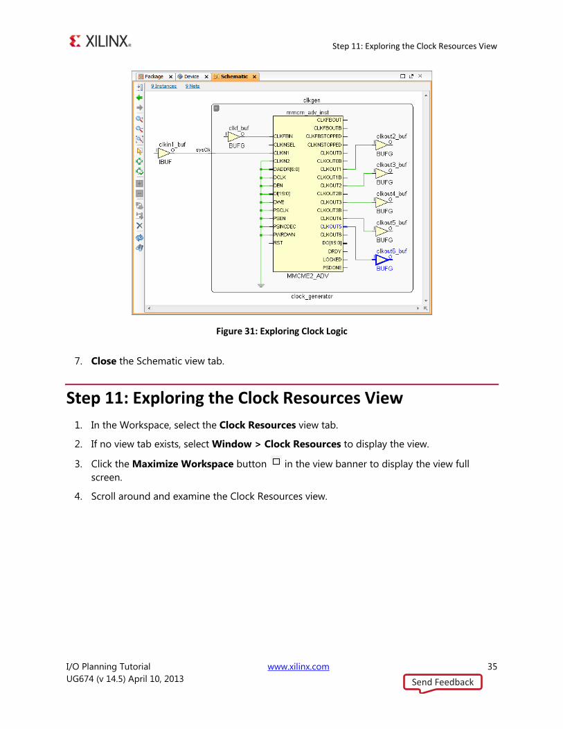
Figure 31: Exploring Clock Logic
Close the Schematic view tab. 7.
Step 11: Exploring the Clock Resources View
In the Workspace, select the Clock Resources view tab. 1.
If no view tab exists, select Window > Clock Resources to display the view. 2.
Click the Maximize Workspace button in the view banner to display the view full 3.
screen.
Scroll around and examine the Clock Resources view. 4.
Send Feedback

Step 11: Exploring the Clock Resources View
I/O Planning Tutorial www.xilinx.com 36
UG674 (v 14.5) April 10, 2013
Figure 32: Viewing Clock Resources
Clock Regions, I/O and GT Banks, MMCMs, and BUFGs display in the Clock Resources
view arranged in positions relative to their location on the actual device. Device
resources are listed under the Site column. Design logic that is assigned to device
resources is listed under the Instance column. You can place clock logic and related I/O
logic into the Clock Resources view by selecting it and dragging it from another view.
You can expand or collapse sections of the Clock Resources view to hide or display the
resources as needed. In Figure 32 you will notice that the Top Half of the device is
collapsed, and can be expanded by clicking on the ‘+’ sign.
Send Feedback

Step 12: Placing the MCM Instance
I/O Planning Tutorial www.xilinx.com 37
UG674 (v 14.5) April 10, 2013
Step 12: Placing the MCM Instance
Click the Find Results view tab on the bottom of the screen to display the view 1.
Select the MMCME2_ADV instance and drag it into the Clock Resources view on the 2.
Instance column next to one of the MMCME2_ADV Sites.
TIP: If the instance does not drag out of the Find Results view, expand the Netlist view tab and
drag the MMCM from that view as shown in Figure 33.
Figure 33: Placing MMCM into the Clock Resources view
Close the Find Results view. 3.
In the Clock Resources view, click the Restore Workspace button in the view banner to 4.
return the view layout.
Click the Device view tab in the Workspace. 5.
Send Feedback

Step 13: Running Design Rule Checks
I/O Planning Tutorial www.xilinx.com 38
UG674 (v 14.5) April 10, 2013
Step 13: Running Design Rule Checks
The PlanAhead tool has an extensive set of I/O related design rule checks (DRCs) to ensure that
I/O Ports are assigned appropriately. You can interactively explore and resolve any reported
design rule violations.
Under Netlist Analysis in the Flow Navigator, click Report DRC. 1.
Clear All, then select to enable Bank and IOB rules as shown in Figure 34. 2.
Figure 34: I/O Related DRCs
You can expand the selected rule categories to examine the specific rule types available in
each.
Click ‘+’ to expand and view Bank and IOB rules, and click OK to run the DRC report. 3.
The DRC Violations view opens to display any violations.
Figure 35: Report DRC Violations
Send Feedback

Step 14: Running Simultaneous Switching Noise Analysis
I/O Planning Tutorial www.xilinx.com 39
UG674 (v 14.5) April 10, 2013
The reported violations indicate that the design has several I/O Ports that are missing LOC
and IOSTANDARD constraints. This is due to the fact that you have not placed or configured
all of the ports in the tutorial design. The design will fail to create a bitstream file with these
errors. You could use the techniques described earlier in this tutorial to place and configure
the remaining I/O Ports.
Select one of the Violations and examine the Violation Properties view 4.
The Violation Properties view provides a more detailed explanation of the design rule
violation as shown in Figure 36, and provides links to the specific design objects in violation
of the rule. The links in the Violations Properties view allow you to select and view the logic
objects. In this case, because the violation objects are I/O ports, you can view the objects in
the I/O Ports view.
Figure 36: Violation Properties view
Close the DRC Violations view. 5.
Step 14: Running Simultaneous Switching Noise Analysis
Simultaneous Switching Noise (SSN) analysis can be performed to help identify potential signal
integrity concerns in the device.
Under Netlist Analysis in the Flow Navigator, click Report Noise . 1.
Click OK in the Run SSN Analysis dialog box. 2.
The Noise report view opens as shown in Figure 37.
Send Feedback

Step 15: Saving the Constraint Files
I/O Planning Tutorial www.xilinx.com 40
UG674 (v 14.5) April 10, 2013
Figure 37: Noise Report
Maximize the Noise view using the Maximize button in the view. 3.
Scroll down and expand the list of I/O Banks. 4.
Select Summary in the upper left categories list and examine the information. 5.
Select Messages and Links to examine the information. 6.
Restore the Noise View to its original size and location. 7.
Step 15: Saving the Constraint Files
Through the course of performing this Tutorial, you have made numerous modifications to the
physical constraints in the design. These changes are currently stored in memory, but will need
to be saved to the constraints file prior to closing the design. Use the Save Constraints
command to write the changes into the project constraint files.
TIP: The Save Constraints As command can alternatively be used to create a new constraints set
containing all of the current constraints, while leaving the original constraint set in its original form.
Select File > Save Constraints. 1.
In the Sources view, double-click the top.ucf file under the Constraint folder constr_1 to 2.
open the constraints file.
Notice the new physical constraints applied.
Close the top.ucf file. 3.
Send Feedback

Conclusion
I/O Planning Tutorial www.xilinx.com 41
UG674 (v 14.5) April 10, 2013
Close the PlanAhead Tool
From the main menu, select File > Exit to close the PlanAhead tool. 1.
Click OK. 2.
Conclusion
In this tutorial, you:
Used the I/O pin planning environment to explore device resources and define alternate
compatible devices for the design.
Imported, created, and configured I/O Ports.
Created Interfaces by grouping the related I/O Ports together.
Used the semi-automatic placement modes to assign critical I/O Ports to package pins.
Placement of the remaining I/O Ports was done using automatic placement.
Exported and examined the I/O Ports list, which can be used for HDL header or PCB
schematic symbol generation.
Opened a netlist-based project and placed GTXE, MMCM_ADV, and BUFG objects using
logic connectivity as a guide for correct placement.
Ran DRCs and Noise Analysis to validate legal I/O placement.
Updated the constraint files with the interactive assignments.
Send Feedback