Embed Size (px)
Citation preview

Exploring Protel 99 SE
Altium Sales and Support Centers
Introductory Tutor ia l
Visit www.protel.com for Reseller contact details in other countries
A Step-by-Step
Introduction to Protel 99 SE -
The Complete Board-Level
Design System for
Windows 2000/NT/98/95
Protel and Altium and the Protel and Altium logo are trademarks or registered trademarks of Altium Limited or its
subsidiaries. All other registered and unregistered trademarks referenced herein are the property of their respective
owners and no trademark rights to the same is claimed.
614-
BR
GEE
PB-0
NORTH AMERICA
17140 Bernardo Center Drive,Suite 100 San Diego CA 92128 USASales Phone: 1 (858) 485-4639Sales Fax: 1 (858) 485-4611Toll Free: 1 (800) 544-4186Sales E-mail:[email protected] E-mail:[email protected]
JAPAN
ASAHI-GIN Gotanda Building 7F23-9, Nishi-Gotanda 1-chomeShinagawa-ku Tokyo 141-0031 JapanPhone: +81 3 5436 2501Fax: +81 3 5436 2505Sales E-mail:[email protected] E-mail:[email protected]
Australia
Level 14, 39 Murray StreetHobart TAS 7000 AustraliaPhone: +61 3 6231 4177Fax: +61 3 6231 4167Toll Free: 1 800 030 949Sales E-mail:[email protected] E-mail:[email protected]
EUROPE
Altium (Switzerland)Unterdorfstrasse 1CH-4334 Sisseln SwitzerlandPhone: +41 62 866 41 11Fax: +41 62 866 41 10Sales Email: [email protected] Email: [email protected]
Altium (Germany)Eltinger Straße 61D-71229 Leonberg GermanyTelephone: +49 71 52 979 910Facsimile: +49 71 52 979 9120Sales Email:[email protected] Email:[email protected]
Altium (France)21 Avenue du Québec91951 Les Ulis Cedex FranceTelephone: +33 1 69 59 26 10Facsimile: +33 1 69 59 26 11Sales Email:[email protected] Email:[email protected]
Altium (The Netherlands)Plotterweg 313821 BB Amersfoort The NetherlandsTelephone: +31 33 455 85 84Facsimile: +31 33 455 00 33Sales Email:[email protected] Email:[email protected]

1
Welcome to Protel 99 SE
Welcome to the world of Protel 99 SE – a complete 32-bit electronic design system for Windows 95/98/NT.Protel 99 SE provides a completely integrated suite ofdesign tools that lets you easily take your designs fromconcept through to final board layout.
Protel 99 SE brings to the EDA desktop a new level ofintegration. Unlike other tool suites that provide separateapplications for each phase of the design process, allProtel 99 SE tools run within a single application environment – the DesignExplorer. Start Protel 99 SE and the Design Explorer opens, putting all yourdesign tools at your fingertips. You benefit from a single, consistent, customizableuser environment – no need to grapple with different applications for differentdesign tasks.
A single environment also means Protel 99 SE eliminates import/export hasslesas you progress through the design process. For example, autorouting a board inProtel 99 SE is done directly in the PCB document window at the touch of asingle button – no need to fiddle with separate router files. With Protel 99 SE youcan compile a circuit for implementation in a programmable logic device directlyfrom the schematic, producing an industry-standard JEDEC device programmingfile in a single action.
Simulation is also integrated into Protel 99 SE. You can set up and run mixedanalog/digital simulations directly from the schematic. Protel 99 SE comes withcomprehensive libraries of simulation-ready components, with full support for theindustry-standard simulation language, SPICE 3f5.
Protel 99 SE comes with extensive schematic and PCB footprint libraries. TheProtel Library Development Center continually updates and adds to theselibraries, ensuring you will always be up-to-date with the latest devices andpackaging technologies from all major manufacturers. Updated libraries areavailable for download from the Protel web site at www.protel.com.
Protel 99 SE also includes integrated spreadsheet, charting, text editing andmacro creation tools, allowing you to manage all aspects of a design projectwithout leaving the Design Explorer environment.
Because the Design Explorer is built on an open client/server architecture, youcan extend the functionality of Protel 99 SE with Add-Ons available from bothAltium and third-party vendors. Add-Ons integrate seamlessly into the DesignExplorer environment, providing additional functions and services – extendingthe capabilities of your Protel 99 SE design tools. The Protel web site atwww.protel.com provides an up-to-date list of the latest Add-Ons, many of whichare directly downloadable.
Install Protel 99 SE and you have at your fingertips all the tools you need toproduce sophisticated designs with unprecedented speed and ease.
Welcome to Protel 99 SE ................................................................1
The Protel 99 SE Design Explorer ....................................................2
Working in the Design Explorer ......................................................4
How the design documents are stored 4
Tips on working in the Design Explorer 4
Creating a new design ..................................................................5
Capturing the schematic................................................................6
Creating a new schematic sheet 6
Setting the schematic options 6
Drawing the schematic 8
Locating the component and loading the libraries 8
Placing the components on your schematic 9
Wiring up the circuit 12
Checking the electrical properties of your schematic 14
Designing the PCB ......................................................................16
Creating a new PCB file 16
Adding the PCB footprint libraries 18
Transferring the design 18
Setting up the PCB workspace 19
Defining the layer stack and other non-electrical layers 20
Setting up new design rules 21
Positioning the components on the PCB 22
Global editing 23
Automatically routing the board 24
Manually routing the board 24
Verifying your board design 27
Printing to a Windows printing device 30
Manufacturing output files 31
Simulating the design ..................................................................33
Setting up for simulation 33
Running a transient analysis 34
Further explorations ....................................................................36
Shortcut keys ..............................................................................37
Table of contents

32
, text, etc).
The Protel 99 SE Design Explorer
The Design Explorer is your interface to your designs, and the design tools. To start Protel 99 SE and open the Design Explorer, select Protel 99 SE from theProtel 99 SE Program Group in the Windows Start menu – the Design Explorer will open, ready for work. Before starting your own design you might like toexplore some of the example designs included with Protel 99 SE – these are located in the \Program Files\Design Explorer 99 SE\Examples\ folder.
Active Database
All design documents are
stored in an integrated
design database.
Explorer and Editor Panels
As well as the Design
Explorer navigation
panel, other editor
panels are available for
each editor (schematic,
PCB, text, etc).
System Menu
Click the down-arrow to
display the system menu
– use this to set up the
preferences, compact a
database and customize
the resources.
All other menus and
toolbars automatically
change to suit the
document being edited.
Folder View
Use folders to organize
the design documents.
Right-click to create a
new document, click and
drag to move a document
to a different folder.
Schematic Editor
Note the Tabs at the top
– there are 2 schematics
currently open.
PCB Editor
You can open and
work on the PCB at
the same time.
Help Advisor
Use the natural language
help system to quickly
find the answer to
your question.
Design Window
Displays the documents that are currently open in
this design – there is a Tab for each open document
and folder. The window has been split into 3 regions
to display a folder, a schematic sheet and the PCB.
Navigation Panel
Displays all the documents and folders in
the design database. The active document
is highlighted, right-click on a document
or folder for a menu of options.
Document/Folder Tabs
Each open document and folder has its own Tab (the icon shows the
active Tab). Right-click on a Tab to split the window, click and drag to
move a Tab to a different region of the window.

54
Create folders and store all the documents
for your design in the one design database
opening.To start the tutorial, create a new design database by completing the following steps:
Close any design databases that arecurrently open.Select File » New from the menus.
The New Design Database dialog willappear. Two types of design storageoptions are available – a MS Access
Database, where all the design documentsare stored within the one database file onthe disk drive, and Windows File System,where the design documents are storedseparately on the disk drive. Regardless ofwhich storage option you choose, the wayyou work in the design database is exactlythe same.
For the tutorial we will use an Access database – set the Design Storage Type
to MS Access Database.Type the name Multivibrator.ddb in the Database File Name field. Click the Browse button and navigate to a location where you would like tostore the design.Click OK to close the New Design Database dialog – the new database willopen in the Design Explorer.
You are now ready to start capturing the schematic.
Working in the Design Explorer Creating a new design
Working in the Design Explorer is just likeworking in the Windows File Explorer – if you arefamiliar with the Windows Explorer then you areready to go!
Like the Windows Explorer, there are 2 regions towork in – the navigation panel on the left, thatdisplays the contents of the design in a tree-likestructure, and the view of what is currentlyselected in the tree is displayed on the right.Simply click on a document or folder in the tree todisplay it on the right.
All the documents in a design are displayed in thesame window, each on a separate tab. Right-clickon a tab to split the window and view multipledocuments simultaneously.
How the design documents are stored
Protel 99 SE stores all the design documents –including the schematic sheets, PCB, libraries,simulation results, manufacturing files, and so on –in an integrated design database. There is no needto find and open each document individually, yousimply open the database, and from there you canaccess all of the design documents.
As well as storing documents within a database,you can also create folders to organize thedocuments.
To make it easy to manage all the documents inyour project you can also store any other type ofdocument, including Microsoft Word and Exceldocuments, AutoCAD drawings, and so on, in thedesign database. Documents created by “OLEcompliant servers”, such as Word and Excel, can be opened directly from theProtel 99 SE design database, simply double-click to edit them.
Tips on working in the Design Explorer
• Select File » New to create a new document or folder.
• Right-click in a folder and select Import to import any document into adesign database.
• Right-click on a document (or folder) to export it from the design database.
• Select Design Utilities from the System menu (the down-arrow) to compact anMS Access database.
• Click-and-drag to re-organize documents and folders in a design.
• Hold the CTRL key as you open a design to stop documents automatically re-
The new
Multivibrator design
database open in
the Design Explorer
The first step
is to create a
new design
database

76
Any subsequent menu items will also have hot keys that you canuse to activate the item. For example, the shortcut for selecting theView » Fit Document menu item is to press the V key followed by theD key. Many submenus, such as the Edit » DeSelect menu, can becalled directly. To activate the Edit » DeSelect » All menu item youneed only press the X key (to call up the DeSelect menu directly)followed by the A key.
Next we will set the general schematic preferences:Select Tools » Preferences [shortcut T, P] from the menus to open the schematic Preferences dialog. This dialog allows you to set global preferences that will apply to all schematicsheets you work on.Click on the Default Primitives tab to make it active and enable the Permanent check box. Click the OK button to closethe dialog.
Before you start capturing your schematic, save this schematic sheet:From the menus select File » Save [shortcut F, S].
Your blank sheet will be saved in the Documents folder.
The Multivibrator
design database
open in the Design
Explorer. The
schematic sheet is
open, ready to start
the design.
Creating a new schematic sheet
To create a new blank schematic sheet complete the following steps:In the panel on the left, expand the navigation tree by clicking on the small +symbol next to the Multivibrator.ddb icon.Click on the Documents folder icon to display the contents of the folder onthe right.From the menu bar selectFile » New.In the New Document dialogclick on the Schematic
Document icon to select anew schematic sheet.Click the OK button to closethe dialog and create a newschematic sheet icon in theDocuments folder.The icon is created with a default name. Select Edit » Rename and type in thenew name for the sheet, Multivibrator.sch.Double-click on the Multivibrator.sch icon to open the schematic sheet.
When the blank schematic sheet opens you will notice that the workspacechanges. The main toolbar includes a range of new buttons, two new toolbars arevisible, the menu bar includes new items, and the Panel changes to includeschematic component library management tools.
You can customize many aspects of the workspace. For example, you canreposition the two “floating” toolbars. Simply click-and-hold the title area of thetoolbar and move the mouse to relocate the toolbar. To “dock” the toolbar, moveit to left, right, top or bottom edge of the main window area. To find out how tocustomize other aspects of the workspace, see the topic, Using the DesignExplorer, in the main help file.
Setting the schematic options
The first thing to do before you start drawing your circuit is to set up the appropriate document options. Complete the following steps:
From the menus choose Design » Options, the Document Options dialogwill open. For this tutorial the only change we need to make here is toset the sheet size to standard A4 format. In the Sheet Options tab find theStandard Styles field. Click the arrow next to the entry to see a list ofsheet styles. Use the scroll bar to scroll up to the A4 style and click to select it.Click the OK button to close the dialog and update the sheet size.
To make the document fill the viewing area again, select the View » Fit
Document menu item. In Protel 99 SE you can activate any menu by simplypressing the menu hotkey (the underlined letter in the menu name).
Capturing the schematic
You can save any schematic
sheet as a document
template, allowing you to
include special information
such as a custom company
title block, logo, and so on.
Refer to the Sheet Templates
topic in the Setting Up the
Schematic Workspace
chapter of the Protel 99 SE
Designer’s Handbook for
complete details on creating
a schematic template.
Protel 99 SE has a
multilevel Undo,
allowing you to undo
any number of
previous actions. The
maximum number of
Undo steps is user-
configurable, and
limited only by the
available memory on
your computer.

98
You will notice that a number of libraries appear in the Browse Sch panel,which should be visible behind the open dialog – when you add onelibrary from a library database all libraries in that database are added tothe list of available libraries. Because all simulation-ready libraries arenow in the library list, we will not need to search for the othercomponents.
Close the Find Schematic Component dialog.
The libraries in the Sim.ddb will appear in the Browse Sch panelwhenever the Browse mode at the top of the panel is set to Libraries. Asyou click on a library name in the upper list, the components in thatlibrary are listed below. The component filter in the panel can then beused to quickly locate a component within a library.
Placing the components on your schematic
The first components we will place on the schematic are the twotransistors, Q1 and Q2. For the general layout of the circuit, refer to theschematic drawing shown in Figure 1.
Select View » Fit Document from the menus [shortcut V, D] to ensureyour schematic sheet takes up the full window.Set the Browse mode to Libraries in the Browse Sch Editor Panel.Q1 and Q2 are BJT transistors, click on the BJT.LIB library to make it theactive library.In the Filter section of the panel, type *3904* and press the ENTER key. A list ofcomponents which have the text “3904” as part of their Part Type field will bedisplayed.Click on the 2N3904 entry in the list to select it, then click the Place button.The cursor will change to a cross hair and you will have an outlined version ofthe transistor “floating” on your cursor. You are now in “part placement” mode.If you move the cursor around, the transistor outline will move with it.
Before placing the part on the schematic, first edit its properties.While the transistor is floating on the cursor, press the TAB key. Thisopens the Part dialog for the component.In the Attributes tab of the dialog set the following values: for Footprint,type TO92A and for Designator, type Q1. Leave all other fields at theirdefault values.Click the OK button to return to placement mode.
You are now ready to place the part.Move the cursor (with the transistor symbol attached) to position thetransistor a little left of the middle of the sheet.Once you are happy with the transistor’s position, left-click or pressENTER to “place” the transistor onto the schematic.
Move the cursor and you will find that a copy of the transistor has beenplaced on the schematic sheet, but you are still in “part placement mode”with the part outline floating on the cursor. This feature of Protel 99 SE allows youto place multiple parts of the same type. So let us now place the second transistor.
Use the filter to
quickly locate
the component
you need
Drawing the schematic
You are now ready to begin capturing (drawing) the schematic. For this tutorialwe will use the circuit shown below. This circuit uses two 2N3904 transistorsconfigured as a self-running astable multivibrator.
Locating the component and loading the libraries
To manage the thousands of schematic symbols included with Protel 99 SE, theSchematic Editor provides powerful library search features. Work through thefollowing steps to locate and add the libraries you will need for the tutorial circuit:
From the menus select Tools » Find Component [shortcut T, O], or press the Find
button in the Schematic Editor Panel. This will open the Find SchematicComponent dialog.First we will search for the transistors, both of which are type 2N3904.Ensure there is a tick in the box next to the By Library Reference field (click inthe check box to enable it if necessary).We want to search for all references to 3904, so in the By Library Reference textfield type *3904* (the * symbol is a wildcard used to take into account thedifferent prefixes and suffixes used by different manufacturers).Ensure that the Search Scope is set to Specified Path, and that the Path fieldcontains the correct path to your schematic libraries. If you accepted thedefault directories during installation, the path should be C:\Program Files\Design
Explorer 99 SE\Library\Sch\. Ensure that the Sub directories and Find All Instances
boxes are ticked.Click the Find Now button to begin the search. There are over 60,000components supplied with Protel 99 SE, so the search may take a couple ofminutes. If you have entered the parameters correctly, 2 libraries will befound and displayed in the Found Libraries list.Click on the BJT.LIB library to select it. This library has symbols for all theavailable simulation-ready BJT transistors. Like all the simulation-readylibraries, the BJT library is in the SIM.DDB library database. Click the Add To Library List button to make this library available to your schematic.
Figure 1
A stable
multivibrator
The link between the
schematic component
and the PCB
component is the
footprint. The footprint
specified in the
schematic is loaded
from the PCB library
when you load the
netlist. Double-click
on a schematic
component to specify
the footprint.

1110
Now place the two capacitors:The capacitor part is also in the Simulation Symbols.Lib library, which shouldalready be selected in the Browse Sch panel.Type *cap* in the Filter in the panel and press the ENTER key.Click on CAP in the components list to select it, then click the Place button. Youwill now have a capacitor symbol floating on the cursor.Press the TAB key to edit the capacitor’s attributes. In the Attributes tab ofthe Part dialog, set the Footprint to RAD0.1, the Designator to C1, and the Part
Type to 20n.Click OK to close the dialog and return to part placement mode.Press the SPACEBAR to rotate the capacitor by 90° so it is in thecorrect orientation.Position and place the two capacitors in the same way that youplaced the previous parts.Right-click or press ESC to exit placement mode.
The last component to be placed is the connector. Connectors arestored in the Miscellaneous Devices.ddb library database.
Using the steps described earlier, add the MiscellaneousDevices.ddb library database to the current library list.Select the Miscellaneous Devices.lib library from the list of librariesin the Browse Sch panel.The connector we want is a two-pin socket, set the Filter to *con2*
and press ENTER.Select CON2 from the parts list and click the Place button. Press TAB toedit the attributes and set Footprint to FLY4 and Designator to Y1. ClickOK to close the dialog.Before placing the connector, press X to flip it horizontally so that it is in thecorrect orientation. Place the connector on the schematic.Right-click or press ESC to exit part placement mode.Save your schematic by selecting File » Save from the menus [shortcut F, S].
You have now placed all the components. Note that the components in Figure 2are spaced so that there is plenty of room to wire to each component pin. This isimportant, you can not place a wire across the bottom of a pin to get to a pinbeyond it, if you do both pins will connect to the wire. If you need to move acomponent click-and-hold on thebody of the component, then drag the mouse to reposition it.
Figure 2
Schematic with
all parts placed
Because this transistor is the same as the previous one, there is no need to editits attributes before we place it. Protel 99 SE will automatically increment acomponent’s designator when you place a series of parts. In this case the nexttransistor we place will automatically be designated Q2.
If you refer to the schematic diagram (Figure 1) you will notice that Q2 isdrawn as a mirror of Q1. To flip the orientation of the transistor that isfloating on the cursor, press the X key. This flips the component horizontally.Move the cursor to position the part to the right of Q1. To position thecomponent more accurately, press the PAGEUP key twice to zoom in twosteps. You should now be able to see the grid lines.Once you have positioned the part, left-click or press ENTER to place Q2.Once again a copy of the transistor you are “holding” will be placed on theschematic, and the next transistor will be floating on the cursor ready to beplaced.Since we have now placed all the transistors, we will exit part placement modeby clicking the right mouse button or pressing the ESC key. The cursor willrevert back to a standard arrow.
Next we will place the four resistors:In the list of libraries in the Browse Sch Panel, scroll down and select the Simulation Symbols.Lib library.
The Simulation Symbols.Lib library includes generic componentssuch as resistors, capacitors, voltage and current sources, andlinear and non-linear dependant sources.
In the Browse Sch panel set the Filter to *res* and press ENTER.Click on RES in the components list to select it, then click thePlace button. You will now have a resistor symbol floating on the cursor.Press the TAB key to edit the resistor’s attributes.In the Attributes tab of the Part dialog, set the Footprint to AXIAL0.4, the Designator to R1, and the Part Type to 100k. Click OK to close the dialog and return to part placement mode.Position the resistor above the base of Q1 (refer to the schematic diagram in Figure 1) and left-click or press ENTER to place the part.Don’t worry about making the resistor connect to the transistor
just yet. We will wire up all the parts later.Next place the other 100k resistor R2 above the base of Q2 (the designatorwill automatically increment when you place the second resistor).The remaining two resistors, R3 and R4, have a value of 1k, so press the TAB
key to call up the Part dialog and change the Part Type field to 1k, then click OK
to close the dialog.Position and place R3 and R4 as shown in the schematic diagram in Figure 1.Once you have placed all the resistors, right-click or press ESC to exit partplacement mode.
Use the following shortcut keys to
change your view of the sheet:
PAGEUP zooms in one step
PAGEDOWN zooms out one step
Shortcuts V,D redraws the sheet
to fit the current window
Shortcuts V,F redraws the sheet
so that all placed objects are
visible in the current window
The END key redraws the screen
To reposition any object, simply
place the cursor directly over the
object, click-and-hold the left
mouse button, drag the object to a
new position and then release the
mouse button.
Use the following
keys to manipulate
the part floating on
the cursor:
Y flips the part
vertically
x flips the part
horizontally
SPACEBAR rotates
the part by 90°
When you are in any editing
or placement mode (a cross
hair cursor is active), moving
the cursor to the edge of
the document window will
automatically pan the
document. If you accidentally
pan too far while you are
wiring up your circuit,
press the V,F key sequence
(equivalent to the View » Fit
All Objects menu item) to
redraw the schematic window,
showing all placed objects.
This can be done even when
you are in the middle of
placing an object.
To edit the
attributes of an
object placed on
the schematic,
double-click the
object to open its
Attributes dialog.

1312
Figure 3
The fully wired
schematic
Wiring up the circuit
Wiring is the process of creating connectivitybetween the various components of your circuit.To wire up your schematic, refer to the diagramin Figure 1 and complete the following steps:
To make sure you have a good view of theschematic sheet, select View » Fit All Objects
from the menus [shortcut V, F].Firstly wire the resistor R1 to the base of transistor Q1 in the followingmanner. Select Place » Wire [shortcut P, W] from the menus or click on the Wire
tool from the Wiring Tools toolbar to enter the wire placement mode. Thecursor will change to a cross hair.Position the cursor over the bottom end of R1. When youare in the right position a circle will appear at the cursorlocation. This indicates that the cursor is over an electricalconnection point on the component.Left-click or press ENTER to anchor the first wire point.Move the cursor and you will see a wire extend from thecursor position back to the anchor point.Position the cursor so that it is below R1 and level with thebase of Q1.Left-click or press ENTER to anchor the wire at this point. Thewire between the first and second anchor points will be placed.Position the cursor over the base of Q1 until you see theconnection circle. Left-click or press ENTER to connect thewire to the base of Q1.Right-click or press ESC to finish placing this particularwire. Note that the cursor remains a cross hair, indicatingthat you are ready to place another wire. (To exit placementmode completely and go back to the arrow cursor youwould right-click or press ESC again – but don’t do this justnow).We will now wire C1 to Q1 and R1. Position the cursorover the left connection point of C1 and left-click or pressENTER to start a new wire.Move the cursor horizontally till it is directly over the wireconnecting the base of Q1 to R1. A connection circle willappear. Left-click or press ENTER to place the wire segment, thenright-click or press ESC to indicate that you have finishedplacing the wire. Note how the two wires are automaticallyconnected.
Wire up the rest of your circuit, as shown in Figure 3.When you have finished placing all the wires, right-click or press ESC to exitplacement mode. The cursor will revert to an arrow.
To graphically edit the shape of
a wire, or any other graphical
object once it has been placed,
position the arrow cursor over
it and left-click once.
Small “editing handles” will
appear at each vertex (corner).
In Protel 99 SE we call this
“focusing” an object.
Click-and-drag an editing
handle to change the shape of
the object.
Whenever a wire runs across
the connection point of a
component, or is terminated on
another wire, Protel 99 SE will
automatically add a junction.
When placing wires, keep in
mind the following points: left-
click or press ENTER to anchor
the wire at the cursor position;
press BACKSPACE to remove the
last anchor point; after placing
the last segment of a wire,
right-click or press ESC to end
the wire placement – the
cursor will remain as a cross
hair and you can begin placing
another wire.
You can start the tutorial at this
point by opening the schematic
Multivibrator placed.sch located
in the download design database
Multivibrator tutorial.ddb
A wire that crosses
the end of a pin will
connect to that pin,
even if you delete
the junction. Check
that your circuit
looks like Figure 3
before proceeding.
Each set of component pins that you have connected to each other now formwhat is referred to as a net. For example, one net includes: the base of Q1, onepin of R1, and one pin of C1.
To make it easy to identify important nets in the design you can add net labels.To place net labels on the 2 power nets complete the following steps:
Select Place » Net Label from the menus. A dotted box will appear floating onthe cursor.To edit the net label before it is placed press the TAB key to displaythe Net Label dialog.Type 12V in the Net field, then click OK to close the dialog.Place the net label such that the bottom left of the net label touchesthe upper most wire on the schematic, as shown in Figure 3. After placing the first net label you will still be in net labelplacement mode, press the TAB key again to edit the second net labelbefore placing it.Type GND in the Net field, click OK to close the dialog, then place thenet label as shown in Figure 3.Select File » Save [shortcut F, S] to save your circuit.
Congratulations! You have just completed your first schematic capture. Before weturn this schematic into a circuit board, let’s take a look at some of the featuresProtel 99 SE includes to help you check your schematic design.

1514
Re-run the ERC by selecting the Tools » ERC menu item [shortcut T, E] andthen clicking the OK button in the Setup Electrical Rule Check dialog.
A text window with the new ERC report will open giving a warning message thatyou have an unconnected input pin in your circuit. A floating input pin error willalso be generated, there is a special option to check for floating input pins in theSetup tab of the ERC dialog.
To view the ERC report and the schematic sheet together, right-mouse clickon the Multivibrator.ERC tab at the top of the ERC text window, then select Split
Horizontal from the floating menu. The design window will split into 2 regions,the upper region displaying the schematic, the lower region the ERC report.Click on the schematic sheet to make it active and then select View » Fit All
Objects from the menus [shortcut V, F] to resize your schematic to fit the newwindow size. Note the crossed red circle on Q1 indicating the error.
When an ERC detects a number of errors in a circuit, you can use Protel 99 SE’s“Cross Probe” feature to easily find particular errors. While only one error ispresent in our circuit, you can see how the Cross Probe feature works bycompleting the following steps:
Click on the tab of the ERC report to make it active. The error information includes designator and pin details (eg Q1-2), and location details (eg @430,390). Double-clickon one of the location details to select it.Click on the Cross Probe tool in the main toolbar. Thecorresponding error will be centered in the schematic window,and the cursor will point to the location.
Before we finish this section of the tutorial, let’s fix theerror in our schematic:
Click on the tab of the schematic sheet to make it active.Select Edit » Undo from the menus [shortcut E, U]. The wire youdeleted previously should now be restored.To check that the undo was successful, re-run the ERC by selecting Tools »
ERC from the menus [shortcut T, E] and clicking OK in the resulting dialog.The ERC report should show no errors.Select File » Close from the menus to close the error report window, thenselect View » Fit All Objects [shortcut V, F] from the menus to restore yourschematic view.
Congratulations! You are ready to transfer the design to PCB layout.
Checking the electrical properties of your schematic
Schematic diagrams in Protel 99 SE are more than just simple drawings – theycontain electrical connectivity information about the circuit. You can use thisconnectivity awareness to verify your design. To do this, perform an ElectricalRules Check (ERC) by completing the following steps:
Select Tools » ERC [shortcut T, E] from themenus. This will open the Setup ElectricalRule Check dialog.The Setup tab of this dialog includes checksfor drafting-type errors. Leave the settingson this tab at their default values.Click on the Rule Matrix tab. This controlsthe electrical characteristics of the ERC.
The matrix gives a graphical representation ofdifferent types of connection points on aschematic and whether they are allowable ornot. For example, look down the entries on theleft side of the matrix diagram and find Output
Pin. Read across this row of the matrix till youget to the Open Collector Pin column. The squarewhere they intersect is red indicating that anOutput Pin connected to an Open Collector Pinon your schematic will generate an errorcondition when the ERC is run. Our circuitcontains only Passive Pins (on resistors,
capacitors and the connector) and Input Pins (on the transistors).
Let’s check to see if the ERC will detect unconnected input pins:Look down the row labels to find Input Pin. Look across the column labels tofind Unconnected. The square where these entries intersect indicates the errorcondition when an Input Pin is found to be Unconnected in the schematic.The default is a yellow square, which indicates that a warning will begenerated for unconnected input pins. Click the OK button to run the ERC. A text window will open with an ERCreport for your circuit.
If your circuit is drawn correctly, the ERC should be blank. If the report giveserrors, check your circuit and ensure all wiring and connections are correct. Ifyou can’t find the error in your schematic, try opening the Multivibrator.Sch file inthe Tutorial_1.ddb download database and repeating the above steps.
We will now deliberately introduce an error into our circuit and re-run the ERC:Click on the Multivibrator.sch tab at the top of the window to make theschematic sheet the active document.Click in the middle of the wire that connects C1 to the base wire of Q1(small, square editing handles will appear at each end of the wire to indicatethat it is focused). Press the DELETE key to delete the wire.
Cross Probing works
between many different
types of documents in
Protel 99 SE. For example,
you can cross probe from a
schematic component to
the corresponding footprint
in a PCB design. The Cross
Probe feature is a powerful
tool when working in
complex designs.

1716
Designing the PCB
Creating a new PCB file
Before you transfer the design from the schematic editor to the PCB editor you needto create the “blank PCB”. The easiest way to create a new PCB design in Protel 99SE is to use the PCBMaker Wizard, which allows you to choose from over 60industry-standard board outlines as well as create your own custom board sizes. Tocreate a new PCB using the PCBMaker Wizard, complete the following steps:
Open the Multivibrator.ddb design database, then click on the Documents folderin the navigation tree on the left.Select File » New from the menus [shortcut F, N], then click on the Wizards tabin the New Document dialog.Click the Printed Circuit Board Wizard icon to select it, then click the OK button to start the Wizard.The first screen you see is the introduction page. Click the Next button to continue.The second page allowsyou to select the boardoutline you wish to use.For this tutorial we willenter our own board size.Select Custom Made Board
from the list of board outlines and then clickthe Next button.In the next page you enter custom boardoptions. For the tutorial circuit a 2 x 2 inchboard will give us plenty of room. Type 2000 in both the Width and Height
fields. Also, turn off the Corner Cutoff and Inner Cutoff options. Leave the otherfields at their default values. Click the Next button to continue. Note that thedefault units for this dialog are mils: 1000mil = 1inch. The next page displays the board outline, you can adjust the sizes ifnecessary. We will leave the options on this page as they are, click the Next
button to continue.The next page allows you to select the physical makeup of the board. Leavethe options on this screen set to their defaults. Click the Next button to continue.The next page allows you to select the types of vias used in the design. Leavethe options on this screen set to their defaults. Click the Next button to continue.The next page allows you to set the routing options. Select the Thru-hole
components option, and set the number of tracks between adjacent pads to One
Track. Click the Next button to continue.The next page allows you to set up some of the design rules that apply toyour board. Leave the options on this screen set to their defaults. Click theNext button to continue.
The next page allows you to save your custom board as a template, allowingyou to create new boards based on the parameters you have just entered. Wedo not want to save our tutorial board as a template, confirm that this optionis unchecked and press the Next button to continue.The PCB Wizard has now collected all the information it needs to createyour new board. Click Finish to close the Wizard. The PCB document editorwill open with your new board outline.Save the document by selecting File » Save from the menus, then closeit by selecting File » Close.The new board has been created with the name PCB1.PCB. Torename the PCB click on the Documents folder in the navigation tree,then click once on the PCB1.PCB icon displayed on the right to selectit. Select Edit » Rename from the menus, type in the new name,Multivibrator.pcb, and press ENTER.Double-click on the Multivibrator.pcb icon to open the PCB, ready to start theboard design.
Adding the PCB Footprint libraries
The PCB
workspace
with the
custom board
outline
The PCB Editor
supports imperial and
metric units. Select
View » Toggle Units
to switch.

1918
Recall that when we placed the components on our schematic, we typed entries inthe Footprint field of each component’s attributes dialog. Before Protel 99 SEknows how to handle the various schematic components you have used in yourcircuit, it needs a representation or “footprint” for each part. The text we typedinto the footprint fields indicates which footprint to use in the PCB design. Protel 99 SE comes supplied with over 35 PCB footprint libraries, including anumber of IPC standard libraries. Before we begin our PCB design we need tomake sure the appropriate footprint libraries are available.
To add the necessary footprint libraries, complete the following steps:Select Design » Add/Remove Library [shortcut D, L] from the menus to open thePCB Libraries dialog.The footprint library databases are located in 3 sub-folders in the \Program
Files\Design Explorer 99 SE\Library\PCB\ folder. Navigate to the \Generic Footprints\
folder to display a list of available generic library databases. For our tutorialwe want two library databases: Advpcb.ddb, which includes a number ofgeneral axial and radial component footprints, and Transistors.ddb, whichcontains transistor footprints. Find and select each of these libraries in turnand press the Add button in the PCB Libraries dialog to add them to theSelected Files list. When you have added both libraries, click the OK button toclose the dialog.To check that the correct libraries are available, select Libraries from the dropdown list in the Browse PCB Editor Panel. PCB Footprints.lib and Transistors.lib
should both appear in the list.Remember that we set the resistors in our schematic to have a footprint entryof AXIAL0.4. To view this footprint, click on PCB Footprints.lib in the librarylist in the Browse PCB Panel. Now scroll down the Components list until yousee the AXIAL0.4 entry. Click on the entry to make it active. A “thumbnail”of the footprint will appear in the MiniViewer window in the PCB EditorPanel, as shown in Figure 4.
We now have all the PCB footprint libraries loaded. Let’s turn our attention toloading our circuit design.
Transferring the design
Transferring the design from the schematic editor to the PCB editor is easy inProtel 99 SE. To transfer the design:
Click on the Multivibrator.sch tab at the top of the design window to make theschematic the active document. Select Design » Update PCB from the menus.
The Update Design dialog will appear. Uncheck the 2 Classes options at thebottom of the Synchronization tab, leave all the other settings at their defaults.
Click on the Preview Changes button at the bottom of the dialog to examinewhat changes will be carried out. The Changes tab should list 35 macros,detailing what components, nets and net nodes will be added to the PCB.
A macro is created for each design change that needs to be performed to get the
contents of the PCB file to correspond to the schematic. Any macro that has anerror listed will not be executed. Click on the Help button for information onresolving macro errors.
Click the Execute button to close the dialog and execute the netlist macros.Once the design transfer is complete, clickon the Multivibrator.pcb tab at the top of thewindow to display the board.
The components in your design will appear tothe right of the board outline. Before we startpositioning the components on the board weneed to set up the PCB workspace.
Setting up the PCB workspace
Before we start positioning the components weneed to ensure that our placement grid is set correctly. All the objects placed inthe PCB workspace are aligned on a grid called the “snap grid”. This grid needsto be set to suit the routing technology that you intend to use. Ourtutorial circuit uses standard imperial components that have aminimum pin pitch of 100mil. We will set the snap grid to an evenfraction of this, say 50 or 25mil, so that all component pins will fallon a grid point when placed. Also, the track width and clearance forour board are 12mil and 13mil respectively (the default values used bythe PCB Board Wizard), allowing a minimum of 25mil betweenparallel track centers. The most suitable snap grid setting would,therefore, be 25mil. To set the snap grid, complete the following steps:
Select Design » Options from the menus [shortcut D, O] to open the DocumentOptions dialog, and click on the Options tab to make it active.Set the value of the Snap X, Snap Y, Component X and Component Y fields of thedialog to 25mil. Note that this dialog is also used to define the electrical grid.The electrical grid operates when you place an electrical object, it overridesthe snap grid and “snaps” electrical objects together.Click OK to close the Document Options dialog.
Let’s set some other options that will make positioning components easier:Select Tools » Preferences from the menus [shortcut T, P] to open the PCBPreferences dialog. In the Editing Options section of the Options tab, ensure theSnap to Center option is checked. This ensures that when you “grab” acomponent to position it, the cursor is set to the component’s reference point.Click the Display tab in the Preferences dialog to make it active. In the Show
section of this tab, uncheck the Show Pad Nets, Show Pad Numbers and Via Nets
options. In the Draft Thresholds section of this dialog, set the Strings field to 4pixels, then close the Preferences dialog.
Figure 5
The components
next to the
board, ready for
positioning
Figure 4
Use the
MiniViewer to
preview the
component
footprints
You can start the tutorial
at this point by opening
the PCB multivibrator
components.pcb in the
download design database
Multivibrator tutorial.ddb
2120
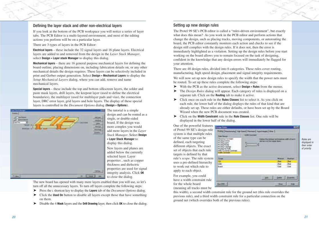
Setting up new design rules
The Protel 99 SE’s PCB editor is called a “rules-driven environment”, but exactlywhat does this mean? As you work in the PCB editor and perform actions thatchange the design, such as placing tracks, moving components, or autorouting theboard, the PCB editor constantly monitors each action and checks to see if thedesign still complies with the design rules. If it does not, then the error isimmediately highlighted as a violation. Setting up the design rules before you startworking on the board allows you to remain focused on the task of designing,confident in the knowledge that any design errors will immediately be flagged foryour attention.
There are 48 design rules, divided into 6 categories. These rules cover routing,manufacturing, high speed design, placement and signal integrity requirements.
We will now set up new design rules to specify the width that the power nets mustbe routed. To set up these rules complete the following steps:
With the PCB as the active document, select Design » Rules from the menus. The Design Rules dialog will appear. Each category of rules is displayed on aseparate tab. Click on the Routing tab to make it active.Click once on each rule in the Rules Classes list to select it. As you click oneach rule, the lower half of the dialog displays the rules of that kind that arealready set up. These rules are either defaults, or have been set up by the BoardWizard when the new PCB document was created.Click on the Width Constraint rule in the Rule Classes list. One rule will bedisplayed in the lower half of the dialog.
One of the powerful featuresof Protel 99 SE’s design rulesystem is that multiple rulesof the same type can bedefined, each targetingdifferent objects. The exactset of objects that each ruletargets is defined by thatrule’s scope. The rule systemuses a pre-defined hierarchyto work out which rule toapply to each object.
For example, you couldhave a width constraint rulefor the whole board(meaning all tracks must bethis width), a second width constraint rule for the ground net (this rule overrides theprevious rule), and a third width constraint rule for a particular connection on theground net (which overrides both of the previous rules).
Defining the layer stack and other non-electrical layers
If you look at the bottom of the PCB workspace you will notice a series of layertabs. The PCB Editor is a multi-layered environment, and most of the editingactions you perform will be on a particular layer.
There are 3 types of layers in the PCB Editor:
Electrical layers – these include the 32 signal layers and 16 plane layers. Electricallayers are added to and removed from the design in the Layer Stack Manager,select Design » Layer stack Manager to display this dialog.
Mechanical layers – there are 16 general purpose mechanical layers for defining theboard outline, placing dimensions on, including fabrication details on, or any othermechanical details the design requires. These layers can be selectively included inprint and Gerber output generation. Select Design » Mechanical Layers to display theSetup Mechanical Layers dialog, where you can add, remove and namemechanical layers.
Special layers – these include the top and bottom silkscreen layers, the solder andpaste mask layers, drill layers, the keepout layer (used to define the electricalboundaries), the multilayer (used for multilayer pads and vias), the connectionlayer, DRC error layer, grid layers and hole layers. The display of these speciallayers is controlled in the Document Options dialog (Design » Options).
The tutorial is a simpledesign and can be routed as asingle, or double-sidedboard. If the design wasmore complex you wouldadd more layers in the LayerStack Manager. Select Design
» Layer Stack Manager todisplay this dialog.
New layers and planes areadded below the currentlyselected layer. Layerproperties , such as copperthickness and dielectricproperties are used for signalintegrity analysis. Click OK
to close the dialog.
The new board has opened with many more layers enabled than you will use, so let’sturn off all the unnecessary layers. To turn off layers complete the following steps:
Press the L shortcut key to display the Layers tab of the Document Options dialog.Click the Used On button to disable all layers except those that have somethingon them.Disable the 4 Mask layers and the Drill Drawing layer, then click OK to close the dialog.
Rules are
displayed in
their order
of priority

2322
component comments (values), as these will not berequired on the final board.
Protel 99 SE also includes powerful interactiveplacement tools, let’s use these to ensure that the 4resistors are correctly aligned and spaced.
Holding the SHIFT key, left-click on each of the 4resistors to select them. Each resistor’s color willchange to the selection color (the default is yellow).Click on the Align Tops of Selected Components buttonon the Component Placement toolbar – the fourresistors will align along their top edge.Now click on the Make Horizontal Spacing of Selected
Components Equal button on the Component Placement
toolbar.Press the X, A shortcut keys to deselect all the resistors.
The four resistors are now aligned and equally spaced.
Global editing
Both the schematic and the PCB editors include a powerful editing aid – referredto as global editing. Global editing is the ability to apply the same change thatyou are currently making, to other objects in the workspace. Let’s do an exampleto demonstrate it.
You have finished positioning the components and you decide that you do notwant the component comments to be displayed. To hide all the componentcomments complete the following steps:
Double-click on one of the comment strings to open its Comment dialog,then click to enable the Hide option.To apply this change globally to all components, click on the Global button.This displays the global editing options for the dialog.
There are now 3 sections to the dialog; theoriginal attributes on the left, the Attributes to
Match By in the center, and the Copy Attributes onthe right.
The options in the Attributes to Match By sectiondefine which other comment strings you wantthis change to apply to. For example, if youonly needed to change the attributes of a fewof the comment strings you could select thosestrings first, then during the global edit youwould match by Selection, targeting only therequired comment strings.
In this case we want the change to applyto all the comment strings so leave the Attributes to Match By optionsunchanged. The options in the Copy Attributes section define what changes will be copied
Currently there is one width constraint rule for your design, which applies to thewhole board. We will now add 2 new width constraint rules, one for the 12V netand another for the GND net.
To add new width constraint rules complete the following steps:Click the Add button to add a new width constraint rule. Like all the ruledefinition dialogs, there are 2 regions to the Max-Min Width Rule dialog. Onthe left of the dialog you define the scope (what you want this rule to target),and on the right of the dialog you define the rule attributes. Let’s set this rule up to target the 12V net. Select Net from the Filter Kind list.When you do a new field titled Net will appear, select 12V from this list.In the Rule Attributes section of the dialog change the Minimum Width, Maximum
Width and Preferred Width fields to 25mil, then click OK to close the dialog.The lower region of the Design Rules dialog now includes the new widthconstraint design rule.Now add another new width constraint design rule for the GND net.Double-click to edit the original Board scope width rule, and confirm thatthe Minimum Width, Maximum Width and Preferred Width fields are all set to 12mil. Close the Design Rules dialog.
When you route the board all tracks will be 12mils wide, except the GND and12V tracks, which will be 25mils.
Positioning the components on the PCB
Before we start positioning the components on the PCB let’s change the view tozoom in to the board:
Press the V, F shortcut keys to zoom in on the board and components.To place the connector Y1, position the cursor over the middleof the outline of the connector, and click-and-hold the leftmouse button. The cursor will change to a cross hair and jumpto the reference point for the part.While continuing to hold down the mouse button, move themouse to “drag” the component.While dragging the connector, press the SPACEBAR to rotate it by90°, and position it toward the left-hand side of the board(ensuring that the whole of the component stays within theboard boundary), as shown in Figure 6.When the component is in position, release the mouse button to“drop” it into place. Note how the connection lines drag withthe component.Reposition the remaining components, using Figure 6 as a
guide. Use the SPACEBAR key as necessary to rotate components as you dragthem, so that the connection lines are as shown in Figure 6. Don’t forget tore-optimize the connection lines as you position each component.
Component text can be repositioned in a similar fashion – click-and-hold to dragthe text, press the SPACEBAR to rotate it. Before repositioning the text we will useProtel 99 SE’s powerful global editing in the next part of the tutorial to hide the
Figure 6
Components
placed on
the PCB
The connection lines are
automatically re-optimized
as you move a component.
In this way you can use the
connection lines as a guide
to the optimum position
and orientation of the
component as you place it.
The thicker green/red line
is a placement force vector,
it indicates better/worse
placement locations.

2524
be situations where you will need exact control over theplacement of tracks – or you may want to route the boardmanually just for the fun of it! In these situations you canmanually route part or all of your board. In this section ofthe tutorial we will manually route the entire board“single-sided”, with all tracks on the bottom layer:
To remove the tracks placed by the autorouter, selectTools » Un-Route » All from the menus [shortcut U, A].The board will be completely un-routed.
We will now place tracks on the bottom layer of the board,using the “ratsnest” connection lines to guide us.
In Protel 99 SE, tracks on a PCB are made from a series ofstraight segments. Each time there is a change of direction,a new track segment begins. Also, by default Protel 99 SEconstrains tracks to a vertical, horizontal or 45° orientation,allowing you to easily produce professional results (thisbehavior can be customized to suit your needs, but for thistutorial we will stay with the default).
Select Place » Interactive Routing from the menus[shortcut P, T] or click the Interactive Routing button onthe Placement toolbar. The cursor will change to across hair indicating you are in track placement mode.Examine the layer tabs that run along the bottom ofthe document workspace. The TopLayer tab shouldcurrently be active. To switch to the bottom layerwithout dropping out of track placement mode, pressthe * key on the numeric keypad (this key togglesbetween the available signal layers). The BottomLayer
tab should now be active.Position the cursor over the bottom-most pad on theconnector Y1. Left-click or press ENTER to anchor thefirst point of the track.Move the cursor towards the bottom pad of theresistor R1. Note how the track is laid. By default,tracks are constrained to vertical, horizontal or 45°directions. Also note that the track has two segments.The first (coming from the starting pad) is solid blue.This is the track segment you are actually placing.The second segment (attached to the cursor) is calledthe “look-ahead” segment and is drawn in outline.This segment allows you to look ahead at where thenext track segment you lay could be positioned sothat you can easily work your way around obstacles,maintaining a 45°/90° track orientation.Position the cursor over the middle of the bottom pad
to each of the matched objects. Ensure that the Hide option in the Copy
Attributes section has a tick next to it.Set the Change Scope at the bottom of the dialog to All primitives (freeprimitives are those primitives that are not part of a component).Click the OK button to close the dialog. A confirmation message will appearasking if you want to make 8 changes. Click Yes to apply the changes.
The comment string for each component will disappear. You can unhide acomponent comment by double-clicking on the component.
Now reposition the component designator strings.When you have finished repositioning the component designators save yourboard by selecting File » Save from the menus [shortcut F, S].
With everything positioned it’s time to lay some tracks!
Automatically routing the board
Routing is the process of laying tracks and vias on the board to connect thecomponents. Protel 99 SE makes the job of routingeasy by providing a number of sophisticated manualrouting tools as well as a powerful and easy-to-useshape-based autorouter, which optimally routes thewhole or part of a board at the touch of a button. Tosee how easy it is to autoroute with Protel 99 SE,complete the following steps:
Select Autoroute » All from the menus [shortcut A,
A]. The Autorouter Setup dialog will appear, click the Route All button to routethe board.When the autorouter has finished, press the END key to redraw the screen.
It’s as simple as that! Protel 99 SE’s autorouter provides results comparable withthat of an experienced board designer. And because Protel 99SE routes your board directly in the PCB window, there is noneed to wrestle with exporting and importing route files.
Select File » Save [shortcut F, S] to save your board.
Note that the tracks placed by the autorouter appear in twocolors: red indicates that the track is on the top signal layer ofthe board, and blue indicates the bottom signal layer. Thelayers that are used by the autorouter are specified in theRouting Layers design rule, which was set up by the boardWizard. You will also notice that the 2 power net tracksrunning from the connector are wider, as specified by the 2new Width Constraint design rules you set up. Don’t worry if the
routing in your design is not exactly the same as Figure 7, the componentplacement will not be exactly the same, so neither will the routing be.
Manually routing the board
While autorouting provides an easy and powerful way to route a board, there will
note how theconnection line guides you to the target pad
segment you are currently placing
look-ahead segment
position the cursorover the pad on R1
click a 2nd time to place this tracksegment
3rd click to place the nexttrack segment,you have now routedthis connection
1st click starts you
placing a track – now
move the cursor toward
the bottom pad on R1
Figure 7
Fully
autorouted
board
You can start the tutorial at
this point by opening the PCB
multivibrator placed.pcb in the
download design database
Multivibrator tutorial.ddb

2726
time to redraw the screen to fit all objects.• Press the PAGEUP and PAGEDOWN keys at any time to zoom
in or out, centered on the cursor position.• Press the BACKSPACE key to “un-place” the last track
segment.• Right-click or press the ESC key when you have
finished placing a track and want to start a new one.• You cannot accidentally connect pads that should not
be wired together. Protel 99 SE continually analyzesthe board connectivity and prevents you from makingconnection mistakes or crossing tracks.
• To delete a track segment, left-click on it to focus it.The segment’s “editing handles” will appear (the restof the track will be highlighted in yellow). Press the DELETE key to clearthe focused track segment.
• Re-routing is easy in Protel 99 SE – simply route the new tracksegments, when you right-click to finish the old redundant tracksegments will automatically be removed.
• When you have finished placing all the tracks on your PCB, right-clickor press the ESC key to exit placement mode. The cursor will change backto an arrow.
Congratulations! You have manually routed your board design.
Because we originally defined our board as being double-sided in the PCBMakerWizard, you could manually route your board “double-sided” using both the topand bottom layers. To do this, un-route the board by selecting Tools » Un-Route » All
from the menus [shortcut U, A]. Start routing as before, but use the * key to togglebetween the layers while placing tracks. Protel 99 SE will automatically insertvias if necessary when you change layers.
Verifying your board design
Protel 99 SE provides a rules-driven environment in which to design PCBs, andallows you to define many types of design rules to ensure the integrity of yourboard. Typically you set up the design rules at the start of the design process, thenverify that the design complies with the rules at the end of the designprocess.
Earlier in the tutorial we examined the routing design rules andadded 2 new width constraint rules. We also noted that there werealready a number of rules that had been created by the boardcreation wizard.
To verify that the routed circuit board conforms to the design rules,we will now run a Design Rule Check (DRC):
Choose Design » Options from the menus [shortcut D, O], and if necessary clickthe Layers tab to make it active.In the System section of this dialog, ensure that the DRC Errors option ischecked.
of resistor R1 and left-click or press the ENTER key. Note that the first tracksegment turns yellow, indicating that it has been placed. Move the cursoraround a little and you will see that you still have two segments attached tothe cursor: a solid blue segment that will be placed with the next mouseclick, and an outlined “look-ahead” segment to help you position the track.Re-position the cursor over the bottom pad of R1. You will have a solid bluesegment extending from the previous segment to the pad. Left-click to placethe solid blue segment. It will turn yellow, indicating it has been placed.
You have just routed the first connection.Move the cursor to position it over the bottom pad of resistor R4. Note asolid blue segment extends to R4. Left-click to place this segment. It willnow turn yellow.Now move the cursor to the bottom pad of resistor R3. Note that thissegment is not solid blue, but drawn in outline indicating it is a look-aheadsegment. This is because each time you place a track segment the modetoggles between starting in a horizontal/vertical direction and starting at 45°.Currently it is in the 45° mode. Press the SPACEBAR key to toggle the segmentstart mode to horizontal/vertical. The segment will now be drawn in solidblue. Left-click or press the ENTER key to place the segment.Move the cursor to the bottom of resistor R2. Once again you will need topress the SPACEBAR key to toggle the segment start mode. Left-click or pressthe ENTER key to place the segment.You have now finished routing the first net. Right-click or press the ESC keyto indicate that you have finished placing this track. The cursor will remain across hair, indicating that you are still in track placement mode, ready toplace the next track. Press the END key to redraw the screen so that you canclearly see the routed net.You can now route the rest of the board in a similar manner to that describedin the previous steps. Figure 8 shows the manually routed board.Save the design.
Keep in mind the following points as you areplacing the tracks:
• Left-clicking the mouse (or pressingthe ENTER key) places the tracksegment drawn in solid color. Theoutlined segment represents the look-ahead portion of the track. Placedtrack segments are shown in yellow.
• Press the SPACEBAR key to togglebetween the start horizontal/verticaland start 45° modes for the tracksegment you are placing.
• Press the END key at any time toredraw the screen.
• Press the V, F shortcut keys at any
Figure 8
Manually
routed board,
with tracks
placed on the
bottom layer
Note that the look-ahead segment is clipping
(no longer attached to the cursor). The PCB
Editor will prevent you from accidentally
placing a track across another object that
would cause a violation. This connection
must be routed around the capacitor.
You can start the tutorial at
this point by opening the
PCB multivibrator
routed.pcb in the download
design database
Multivibrator tutorial.ddb

28 29
Click the OK button to close the dialog.Choose Tools » Design Rule Check from the menus [shortcut T, D].Both the on-line and batch DRC options are configured in theDesign Rule Check dialog. Leave all options at their defaultsand click the Run DRC button.
The DRC will run and the results will be displayed in a text file.Look through this DRC report file. It lists each active design rule,and any violations that occur in the PCB design. Notice that thereare four violations listed under the Clearance Constraint rule. Thedetails show that the pads of transistors Q1 and Q2 violate the13mil clearance rule. If you switch to your PCB document, youwill see that the transistor pads are highlighted in green, indicatinga design rule violation.
Normally you would set up the clearance constraint rules beforelaying out your board, taking account of routing technologies andthe physical properties of the devices. Let’s analyze the error thenreview the current clearance design rules and decide how toresolve this situation.
To find out the actual clearance between the transistor pads:With the PCB document active, position the cursor over themiddle of one of the transistors and press the PAGEUP key tozoom in.
Select Reports » Measure Primitives from the menus [shortcut R, P]. The cursorwill change to a cross hair and you will be prompted on the status bar to“Choose First Primitive”.Position the cursor over the middle of the lower pad on the transistor and left-click or press ENTER. Because the cursor is over both the pad and the trackconnected to it, a menu will pop up to allow you to select the desired object.Select the transistor pad from the popup menu.Position the cursor over the middle of one of the other transistor pads and
left-click or press ENTER. Once again select the pad from the popup menu.
An information box will open showing theminimum distance between the edge of the twopads is 10.711mil.
Close the information box, then right-click orpress ESC to exit the measurement mode, usethe V, F shortcut to re-zoom the document.
Let’s look at the current clearance design rules.Select Design » Rules from the menus
[shortcut D, R] to open the Design Rules dialog.Click on the Routing tab to make it active, then in the Rule Classes list clickonce on the Clearance Constraint to select it. The region at the bottom of thedialog will contain a single rule, specifying that the minimum clearances for
the whole board are 13mil. The clearance between the transistorpads is less than this, which is why they generate a violation when we run a DRC.
We now know the minimum distance between transistor pads is a littleover 10mil, so let’s set up a design rule that allows the clearanceconstraint to be 10mil for the transistors only.
Click the ADD button to add a new clearance constraint rule.In the Rule Attributes section of the resulting dialog, set the Minimum Clearance to 10mil.In the Rule Scope section,use the drop-down list to change the first Scope Kind
field to Footprint-Pad.Select TO92A in the Footprint field.Type an * (asterisk) in the Pad field,indicating “any pad” on the TO92A.Click OK to close the dialog.
The new rule will appear in the lowerregion of the Design Rules dialog.
You can now re-run the DRC from the Design Rules dialog by clicking the Run DRC button, then clicking the Run DRC button in the Design RulesCheck dialog.
A new report will be generated – this report should show no rule violations.
You have completed the PCB layout, and are ready
to produce the output documents.
You can also use the PCB
editor panel to find design rule
violations. Set the Browse
mode at the top of the panel
to Violations, then use the
Details, Highlight and Jump
buttons to find and analyze
the design rule errors.
To make it easier to see the
design rule violations you can
display the primitives in draft
mode. Select Tools »
Preferences, click on the
Show/Hide tab, then click the
All Draft button. When you
close the dialog all primitives
will be shown in draft mode,
except those that are marked
with a DRC error marker. Click
the All Final button in the
Show/Hide tab to display the
primitives as solids again.
Protel 99 SE supports
fully-hierarchical design
rules. You can set any
number of rules of the
same class, each with a
defined scope. The rule
scope determines the
rule’s precedence.

30 31
Printing to a Windows printing device
Once the layout and routing of the PCB is complete you are ready to produce theoutput documentation. This documentation might include a manufacturing drawingdetailing the fabrication information, and assembly drawings detailing componentlocation information and loading order.
To produce these drawings Protel 99 SE includes a sophisticated printing engine,called Power Print, that gives you complete control over the printing process.Using Power Print you first preview the drawings (called printouts), where you candefine precisely what mix of PCB layers you want to print, set the scaling andorientation, and see exactly how it will look on the page before you print it.
Print/preview setups are stored as .PPC documents in your design – they can berenamed, reopened at any time, and copied from one design to another.
To create a print preview document:Select File » Print/Preview from the PCB menus.
The PCB will be analyzed, and a default printout displayed in a new PPCwindow. The default composite preview includes 1 printout.
To examine the set of PCB layers that are included in the printout,click on the Browse PCBPrint tab at the top of the panel to display theprintout set, then click on the small + symbol to expand theMultilayer Composite Print, as shown in Figure 9.
A print preview document (.PPC) can include any number of printouts, and eachprintout can include any combination of layers, overlaid in any order you require.
To change the default composite printout to a composite drill guide,select Tools » Create Composite Drill Guide from the menus, clicking Yes in the Confirm Create Print-Set dialog.
The PCB is re-analyzed, and a new printout displayed.Click on the small + symbol next to the Combination Drill Guide
printout in the Browse PCBPrint panel to display the layers in the printout.
This printout includes both the drill guide, a system layer which includes asmall cross at each drill site, and the drill drawing layer, which includes aspecial shape at each drill site, unique for each drill size.
The drill guide layer is not required in a typical drill drawing, toremove it right-click on the DrillGuide layer in the panel and select Delete
from the floating menu.
Note the printer icon at the top of the Browse PCBPrint panel – theprintouts will target your default windows printer.
To change the target printer, and set the page orientation andscaling, select File » Setup Printer from the menus – then choose yourpreferred printer and set the Orientation to landscape in the PCBPrint Options dialog.
The preview will be re-analyzed and displayed, ready for printing.Select File » Print All from the menus to print the drill drawing. For information onthe various printing options refer to the Print Options menu item in the Help menu.
Manufacturing output files
The final phase of the PCB design process is to generate the manufacturing files.The set of files that are used to manufacture and fabricate the PCB include Gerberfiles, NC drill files, pick and place files, a bill of materials and testpoint files.
All of these files are configured in and produced by Protel 99 SE’s CAMManager. The setups for the manufacturing documents are stored in a .CAMdocument in the design database.
To create the manufacturing files for the tutorial PCB, make the PCB theactive document, then select File » CAM Manager from the PCB Editor menus.
A new CAM document is created, and the Output Wizard launched. The Wizard can be used to create each of the supported output file types,click Next to display the list of available types.Select Gerber from the list and click Next for each page of the Wizard, leavingthe options on each page at the defaults, then Finish on the last page. Once the Wizard closes, the CAM document will display one CAM outputsetup, called Gerber Output 1. The setup of the Gerber files can be changed atany time, double-click on the name Gerber Output 1 to display the GerberSetup dialog.
Each Gerber file corresponds to 1 layer in the physical board – the componentoverlay, top signal layer, bottom signal layer, the solder masking layers, and soon. It is advisable to consult with your PCB manufacturer to confirm theirrequirements before generating the Gerber and NC drill files required to fabricateyour design.
Figure 9
Default
composite
printout,
includes all
the used
layers on
the board
Power Print gives
you complete
control over the
printing process
Select Edit » Copy
from the menus to copy
the current printout to
the clipboard and paste
it into another Windows
application.
Select File » Export to
export the printouts to
the hard disk as WMF
or EMF files.

32 33
The output documents have been created
and stored in folders in the design database.
Simulating the design
Protel 99 SE allows you to run a vast array of circuit simulations directly from aschematic. In the following sections of the tutorial we will simulate the outputwaveforms produced by our multivibrator circuit.
Setting up for simulation
Before we can run a simulation we need to add a few things to ourcircuit – a voltage source to power the multivibrator, a groundreference for the simulations, and some net labels on the points ofthe circuit where we wish to view waveforms.
Click on the Multivibrator.sch tab at the top of the window tomake the schematic the active document.
The first step is to replace the connector with a voltage source. To delete the connector, click once on the body of the connector to focus it (a dotted focus box will appear around the connector), then press the DELETE
key on the keyboard.
At the moment there is not enough room for the voltage source, so we’ll move the free ends of the wires.
To move the dangling end of the 12V wire click once on the wire to focus it.When the small square editing handles appear click once on the handle onthe free end of the wire, then move the handle up almost to where the wirechanges direction (but not all the way up).Click again to “drop” the handle. Repeat this process for the dangling end of the GND wire,moving it toward the bottom of the sheet.Select View » Toolbars » Simulation Sources from the menus todisplay the Simulation Sources toolbar.Click the +12V source button on the Simulation Sources
toolbar. A source symbol will appear floating on the cursor. Press the TAB keyon the keyboard to edit its attributes. In the resulting dialog, click theAttributes tab to make it active and set the Designator field to V1. Leave theFootprint field blank. Click the OK button to close the dialog and then place thesource between the dangling ends of the 12V and GND wires.Using the same technique you used to move the dangling ends of the 12Vand GND wires apart, move them again to attach each wire end to either endof the voltage source, as shown in Figure 10.
Our last task before running a simulation is to place net labels at appropriatepoints on the circuit so we can easily identify the signals we wish to view. Inthe tutorial circuit the points of interest are the base and collectors of the twotransistors.
Select Place » Net Label from the menus [shortcut P, N]. Press the TAB keyto edit the net label attributes. In the resulting dialog, set the Net fieldto Q1B and close the dialog.Position the cursor over the wire coming from the base of Q1. Left-click orpress ENTER to place the net label on the wire.
To include a Bill of Materials in the Outputsetups, right-click in the CAM document and select Insert Bill of Materials from thefloating menu.In the Bill of Materials Setup dialog enablethe Text format, disable the other 2 formats,and click OK to close the dialog. Note that 3formats are supported, Text, CSV (CommaSeparated Values), which loads straight into aspreadsheet editor or can be imported into adatabase, and Spreadsheet, which automaticallyopens in Protel 99 SE’s spreadsheet editor.
You are now ready to generate the Gerber andBOM output documents. Before you do, we willconfigure the generation options.
Select Tools » Preferences from the menus todisplay the CAM Options dialog. Note thatyou can automatically export the documentsto a disk drive. Enable the Separate Folder for Each Output Type
option and click OK to close the dialog.Select Tools » Generate CAM Files from themenus to create the Gerber and BOM files. When the generation process is complete a new folder will appear in thenavigation tree in theExplorer panel, called CAM
for Multivibrator. Click on the small +symbol to expand theview and display the Bom
Output and Gerber Output
sub-folders, then click onthe small + symbol next toeach to display thecontents of each folder.Click on the BOM for
Multivibrator.txt icon toopen the Bill of Materials.
If required, the Gerber files could be exported from the design and shipped to thePCB manufacturer.
Congratulations! You have completed the PCB design process.
You can start the tutorial at
this point by opening the
schematic multivibrator
sim1.sch in the download
design database Multivibrator
tutorial.ddb
The electrical “hot
spot” of a net label
is the bottom left
corner – ensure
that this corner
touches the wire.

3534
Press the TAB key and changethe Net field to Q1C.Position the cursor over thewire coming from the collectorof Q1 and left-click to placethe second net label.Similarly place net labels withdesignators Q2B and Q2C onthe base and collector wires ofQ2 respectively.When you have finishedplacing the net labels, right-click or press the ESC key toexit placement mode.
To save your simulation-ready circuit with a different name to that of youroriginal schematic, select File » Save As [shortcut F, A] and type Multivibrator
simulation.sch in the Save As dialog.
Running a transient analysis
Your schematic now has all the necessary additions, so let’s set up torun a transient analysis of the circuit.
In our tutorial circuit, the RC time constant is 100k x 20n = 2milliseconds. To view 5 cycles of the oscillation we will set up toview a 10ms portion of the waveform.
Select Simulate » Setup from the menus to display the AnalysesSetup dialog. All the simulation options are set up here.Click on the Transient/Fourier tab at the top of the dialog.
In the Default Parameters region of the dialog disable the Always Set Defaults
option. When you do, the options in the Transient Analysis region of the dialogwill become available.
To specify a 10ms simulation windowset the Stop Time field to 10m.Now set the Step Time field to 10u,indicating that the simulation shoulddisplay a point every 10us (giving 1000display points in all, enough to give anaccurate picture of the results).During simulation the actual timestep isvaried automatically to achieveconvergence. The Maximum Step fieldlimits the variation of the timestep size,set the Maximum Step to 10u.
The last thing to set up is the nodes in the circuit that you wish to observe. To do this:
Click on the General tab in the Analyses Setup dialogIn the Collect Data For field select Node Voltage and Supply Current from the list.This option defines what type of data you want calculated during thesimulation run.In the Available Signals field double-click on the Q1B, Q2B, Q1C and Q2C signalnames. As you double-click on eachone it will move to the Active Signals
field.
You are now ready to run a transientsimulation.
Click on the Run Analyses button atthe bottom of the dialog to run the simulation.The simulation will be performed,when it is finished you should seeoutput waveforms similar to thoseshown in Figure 11.
Congratulations! You have simulatedyour circuit and displayed its outputwaveforms. If you like, you can changethe values of some of the components on your schematic and re-run thesimulation to see the effects. Try changing the value of C1 to 47n (double-click onC1 to edit its attributes) and re-running the transient analysis. The outputwaveforms will show an uneven mark/space ratio.
Figure 11
Output
waveforms
from the
multivibrator
Figure 10
Simulation-
ready
schematic
You can start the tutorial
at this point by opening
the schematic
multivibrator sim2.sch in
the download design
database Multivibrator
tutorial.ddb
Setting up
the transient
analysis

36
Further explorations
This tutorial has introduced you to just some of the powerful features of Protel 99 SE. We’ve captured a schematic, run a transient simulation on thedesign, and designed and routed a PCB, all with the integrated tools provided inProtel 99 SE. But we’ve only just scratched the surface of the design powerprovided by Protel 99 SE.
Once you start exploring Protel 99 SE you will find a wealth of features to makeyour design life easier. To demonstrate the capabilities of the software, a numberof example files are included. You can open these examples in the normal way,select File » Open from the Design Explorer menus then navigate to the \Program
Files\Design Explorer 99 SE\Examples\ folder. As well as the board design examplesin this folder, there are a number of sub-folders with examples that demonstratespecific features of Protel 99 SE.
Check out the \Circuit Simulation\ sub-folder to explore Protel 99 SE’s analogand digital simulation capabilities. Aswell as analog examples thatdemonstrate various circuit designs,such as amplifiers and power supplies,there are mixed-mode examples, amath function example, an examplethat includes linear and non-lineardependent sources (741 OperationalAmplifier.ddb), and even a vacuumtube example!
If you’re interested in PLD design,the \PLD\ sub-folder has a number of schematic-based pld designs, includingWait.ddb which can be compiled to produce the JEDEC download file. If you’reinterested in implementing a PLD design using a Hardware Description Language,the \Reference\ sub-folder includes a number of designs that demonstrate thevarious capabilities of Protel 99 SE’s CUPL HDL, including simulating the PLDdesign.
With faster logic switching and design clock speeds, the quality of the digitalsignals becomes more important. Protel 99 SE includes a sophisticated signal
integrity analysis tool that can accurately model and analyze your board layout. Thesignal integrity requirements such as impedance, overshoot, undershoot, andslope are defined as PCB design rules, and then tested during the standard designrule check. If there are nets that you need to analyze in more detail you can selectTools » Signal Integrity to pass the design to the Signal Integrity Analyzer, where youcan perform reflection and cross talk simulations. The results are displayed in anoscilloscope-like waveform analyzer, where you can examine the performanceand take measurements directly from the waveforms.
If you are interested in exploring Protel 99 SE’s signal integrity analysis featureswhy not download the Signal Integrity Analysis Introduction PDF file from thedownload page of Protel’s web site, www.protel.com.
Check out the
extensive
examples to
explore more of
Protel 99 SE’s
design
capabilities
Shortcut keys
Common Schematic and PCB Shortcuts
Keys Function
Left-click Focus object
Left double-click Edit object
Left-click and hold Move object/selection
Left-click, Select inside area
hold and drag
Shift+left-click Select/deselect object
Right-click Popup floating menu/esc from current
operation
X, A De-select all
Alt+Backspace Undo
Ctl+Backspace Redo
V, D View Document
V, F View Fit placed objects
PageUp Zoom in (zooms around cursor, position
the cursor first)
PageDown Zoom out
Home Redraw screen with center at the cursor
point
End Redraw the screen
Spacebar Abort screen re-draw
Tab While an object is floating on the cursor
to edit its attributes
Shift While autopanning to pan at higher speed
X Flip object along the X-axis
Y Flip object along the Y-axis
M Pop-up Move sub-menu
S Pop-up Select sub-menu
Esc Escape from current process
Schematic Shortcuts
Keys Function
Insert While placing an object to clone a placed
object (of the same kind)
Backspace While laying a wire/bus/line/
polygon to delete the last vertex
Spacebar While placing to rotate object by 90
degrees
Ctrl+click Drag object, maintaining wire
(then release Ctrl) connectivity
Ctrl (hold) Temporarily disable the Snap grid
Left-click and hold, When a wire is focused
then press Insert to add a vertex
Left-click and hold, When a wire is focused to
then press Delete delete a vertex
PCB Shortcuts
Keys Function
Q Toggle units (metric/imperial)
Ctrl+click Drag track/drag track end
Ctrl+shift+click Break track
Backspace Remove last track corner during track
placement
Ctrl Disable the Electrical grid during placement
Alt Temporarily switch from Avoid Obstacle to
Ignore Obstacle mode
Ctrl+Spacebar Cycle through connection lines on a pad
when routing
Right-click and hold Display slider hand and slide view of PCB
G Pop up snap grid menu
Ctl+G Pop up snap grid dialog
Shift+E Toggle electrical grid on/off
Shift+R Cycle through routing modes (ignore obstacle,
avoid obstacle, push obstacle)
Shift+S Toggle single layer mode on/off
L Layers Tab of Document Options dialog
Ctl+Delete Clear all selected
Ctl+H Select connected copper
Spacebar Rotate object being moved (anti-clockwise)
Shift+Spacebar Rotate object being moved (clockwise)
Spacebar Toggle start/end mode during track placement
Shift+Spacebar Cycle through all placement modes during
track placement
Ctrl+Spacebar Cycle through connection line on a pad - use
this after starting to route from a pad with
multiple connection lines
L Flip component being moved to the other side of board
N Hide net connections while moving a component
* Cycle through signal layers (numeric keypad)
+ Cycle forwards through layers (numeric keypad)
- Cycle backwards through layers (numeric keypad)
Design Explorer Shortcuts
Keys Function
Ctrl (during file open) Open design without re-opening documents
Tab Switch from Panel to active document/folder
Shift+Tab Switch from text document to Navigation
Panel
Ctrl+Tab Cycle through open documents/folders
Ctrl+F6 Cycle through open design databases
Ctrl+F4 Close active document/folder
Alt+F4 Close Design Explorer
F5 Refresh the display