Embed Size (px)
Citation preview
LOT Chair of Surfaceand MaterialsTechnology
Introduction to Thin Film Technology
Contents1 Introduction and Application Examples (2h)1. Introduction and Application Examples (2h)2. Preparation of Thin Films by PVD (Physical Vapor Deposition) (12h)
2.1 Vacuum Technique (1h)2.1.1 Kinetics of Gases2.1.2 Transport and Pumping of Gasesp p g2.1.3 Pumping Systems
2.2 Evaporation (5h)2.1.1 Thermal Evaporation 2.1.2 Evaporation of alloy and compound films2 1 3 R ti E ti2.1.3 Reactive Evaporation2.1.4 Activated Reactive Evaporation2.1.5 Other modern Evaporation Techniques
2.3 Sputtering (4h)2 2 1 Physical Principals of the Processes2.2.1 Physical Principals of the Processes2.2.2 Further Processes in Film Growth by Sputtering2.2.3 Sputtering of Alloys2.2.4 Reactive Sputtering2.2.5 Technical Setups of Sputteringp p g
2.4 Production of Thin Films by Ions and ionized Clusters2.5 Characteristic Data of the Particles and their Influences on the Growth of the thin films (2 h)
3 Preparation of Thin Films by CVD (Chemical Vapor Deposition) (4h)3.1 Conventional CVD Processes3 2 Pl E h d CVD3.2 Plasma-Enhanced CVD3.3 Surface Modification by Cold Plasma
4 Important Film Systems (2h)4.1 Plasma Decomposition (a-C:H, a-Si:H)4 2 Microwave-Plasma-Enhanced Diamond Deposition
Prof. Dr. X. Jiang, 23.06.2008
4.2 Microwave-Plasma-Enhanced Diamond Deposition4.3 Transparent and conductive oxide films

LOT Chair of Surfaceand MaterialsTechnology
Introduction to Thin Film Technology
DefnitionDefnitionDefnitionDefnition• Chemical Vapour Deposition (CVD) involves the dissociation and/or
chemical reactions of gaseous reactants in a activated (heat, light, plasma) environment, followed by the formation of a stable solid product.
• The deposition involves homogeneous gas phase reactions, which p g g poccur in the gas phase, and/or heterogeneous chemical reactions which occur on/near the vicinity of a heated surface leading to the formation of powders or films, respectively.
• Though CVD has been used to produce ultrafine powders, this lecture is mainly concerned with the CVD of films and coatings.
Prof. Dr. X. Jiang, 23.06.2008

LOT Chair of Surfaceand MaterialsTechnology
Introduction to Thin Film Technology
C ti l CVD P (O di CVD)Conventional CVD Processes (Ordinary CVD)• Reactions driven by thermal energy supplied solely.• Reactants are in ground states• Reactants are in ground states.• Reactions progress under nearly thermodynamic equilibrium.
Plasma (Photon) Enhanced (PE) CVD• Film formation resulting from the reactivity of excited species.• Substrate temperature does not cross over activation energy.• Substrate temperatures much lower than those used in thermal CVD.• Cold plasma is generated at low pressure (0 1 10 Torr)• Cold plasma is generated at low pressure (0.1 – 10 Torr).• MFP is short as several micrometers.• Most electron energies are within a range of 0.5 – 10 eV.g g• Plasma density is not high.
Prof. Dr. X. Jiang, 23.06.2008
LOT Chair of Surfaceand MaterialsTechnology
Introduction to Thin Film Technology
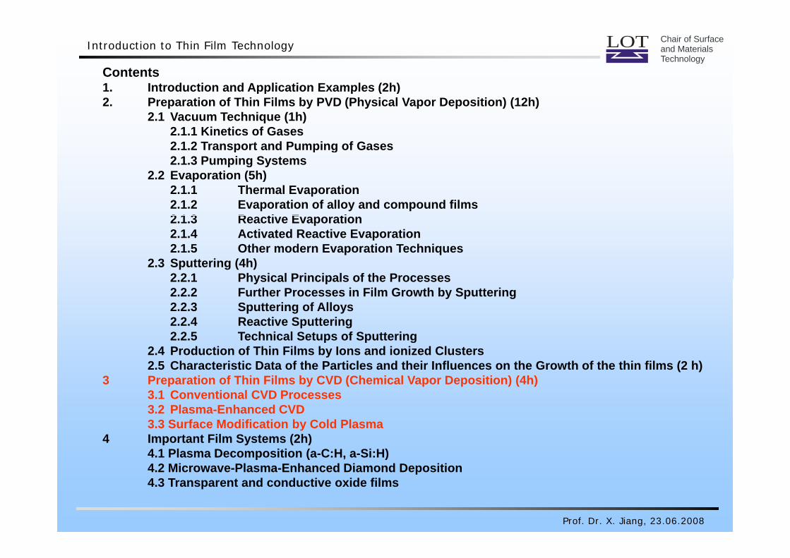
CVD named by parameter applicationsCVD named by parameter applications
1 atmospheric pressure CVD
CVD named by parameter applicationsCVD named by parameter applications
1. atmospheric-pressure CVD
2. Low-pressure CVD
3 Hi h t t CVD3. High-temperature CVD
4. Low-temperature CVD
5. plasma-assisted CVD
6. Photon-enhanced CVD
Prof. Dr. X. Jiang, 23.06.2008

LOT Chair of Surfaceand MaterialsTechnology
Introduction to Thin Film Technology
Conventional CVD ProcessesConventional CVD ProcessesConventional CVD ProcessesConventional CVD Processes1. Decomposition reactions: AB(g) → A(s) + B(g)(g) ( ) (g)
2. Reduction and oxidation reactions: AB(g) + C(g) → A(s) + BC(g)C = hydrogen or metaly g
AB(g) + 2D(g) → AD(s) + BD(g)D = oxygen or nitrogen
3. Hydrolysis reactions: AB2(g) + 2HOH(g) →AO(s) + 2BH(g) + HOH(g)(s) (g) (g)
4. Polymerisation reactions: x A(g) → Ax(s)
5. Transport reactions: A(s) + B(g) ←→ AB(g)T1 → T2 ←
Prof. Dr. X. Jiang, 23.06.2008

LOT Chair of Surfaceand MaterialsTechnology
Introduction to Thin Film Technology
Decomposition reactionsDecomposition reactionsDecomposition reactionsDecomposition reactionsGas dilution hydride system
Ni(CO)4 → Ni + 4CO200 – 300 °C
Ni(CO)4 → Ni 4CO
SiH4 → Si + 2H2800 – 1300 °C
1000 2000 °C
Prof. Dr. X. Jiang, 23.06.2008
CH4 → C + 2H21000 – 2000 C
LOT Chair of Surfaceand MaterialsTechnology
Introduction to Thin Film Technology
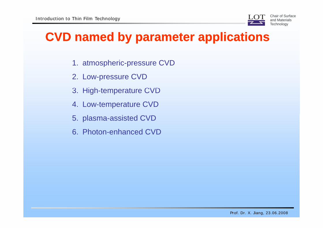
Reduction reactionReduction reactionReduction reactionReduction reactionTo prepare Si single crystalline layer
PumpS bstrateSubstrate
Cool media
Evaporator
SiCl4 + 2 H2 → Si + 4 HCl
Evaporator
Prof. Dr. X. Jiang, 23.06.2008
SiCl4 2 H2 → Si 4 HCl
LOT Chair of Surfaceand MaterialsTechnology
Introduction to Thin Film Technology
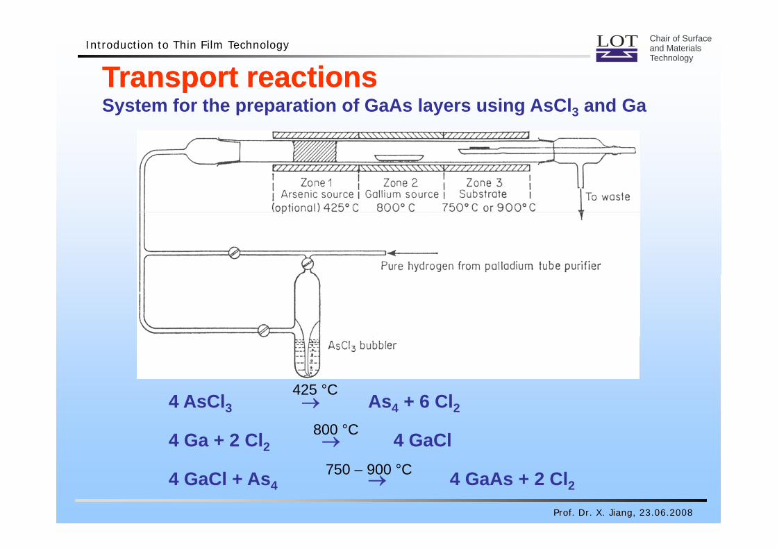
Transport reactionsTransport reactionsppSystem for the preparation of GaAs layers using AsCl3 and Ga
4 AsCl → As + 6 Cl425 °C
4 AsCl3 → As4 + 6 Cl2
4 Ga + 2 Cl2 → 4 GaCl800 °C
Prof. Dr. X. Jiang, 23.06.2008
4 GaCl + As4 → 4 GaAs + 2 Cl2750 – 900 °C

LOT Chair of Surfaceand MaterialsTechnology
Introduction to Thin Film Technology
DisproportionDisproportion – system based on the Si-I2 equilibriumDisproportion Disproportion system based on the Si I2 equilibrium
2 SiI2 → SiI4 + Si
Limitation ofLimitation of conventional CVD = high temperatuire
Prof. Dr. X. Jiang, 23.06.2008
→ PECVD
LOT Chair of Surfaceand MaterialsTechnology
Introduction to Thin Film Technology
Plasma Enhanced Chemical VaporPlasma Enhanced Chemical VaporPlasma Enhanced Chemical Vapor Plasma Enhanced Chemical Vapor DepositionDeposition
• Plasma Deposition
Different Names – the Same Process
Plasma Deposition
• Glow Discharge Deposition
• Plasma Enhanced (Chemical Vapor) Deposition (PECVD)• Plasma Enhanced (Chemical Vapor) Deposition (PECVD)
• Plasma Assisted (Chemical Vapor) Deposition (PACVD)
• El t A i t d (Ch i l V ) D iti (EACVD)• Electron Assisted (Chemical Vapor) Deposition (EACVD)
• Plasma Polymerization
• Glow Discharge Polymerization
Prof. Dr. X. Jiang, 23.06.2008
LOT Chair of Surfaceand MaterialsTechnology
Introduction to Thin Film Technology
Plasma Enhanced Chemical VaporPlasma Enhanced Chemical VaporPlasma Enhanced Chemical Vapor Plasma Enhanced Chemical Vapor Deposition Deposition
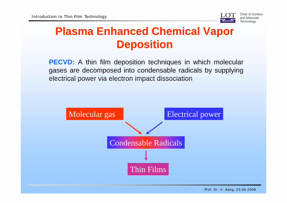
PECVD: A thin film deposition techniques in which moleculargases are decomposed into condensable radicals by supplyingelectrical power via electron impact dissociationelectrical power via electron impact dissociation
Molecular gas Electrical power
Condensable Radicals
Thin Films
Prof. Dr. X. Jiang, 23.06.2008
Thin Films
LOT Chair of Surfaceand MaterialsTechnology
Introduction to Thin Film Technology
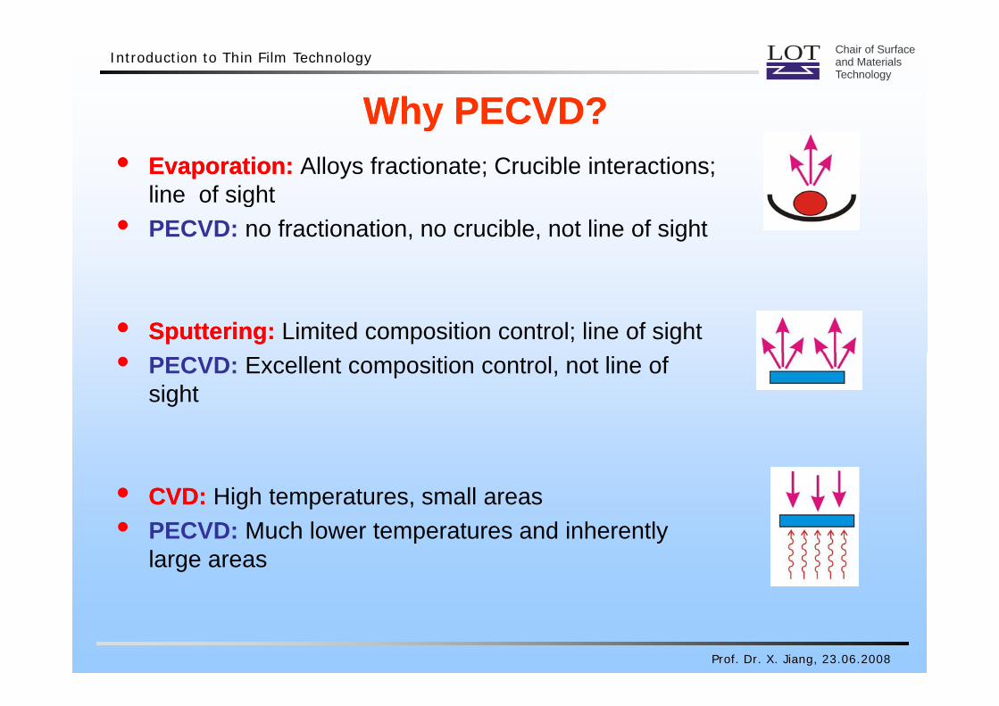
Why PECVD?Why PECVD?Why PECVD?Why PECVD?•• Evaporation:Evaporation: Alloys fractionate; Crucible interactions;
line of sightline of sight• PECVD: no fractionation, no crucible, not line of sight
•• Sputtering: Sputtering: Limited composition control; line of sight• PECVD: Excellent composition control, not line of
sight
•• CVD: CVD: High temperatures, small areas• PECVD: Much lower temperatures and inherently
large areas
Prof. Dr. X. Jiang, 23.06.2008
LOT Chair of Surfaceand MaterialsTechnology
Introduction to Thin Film Technology
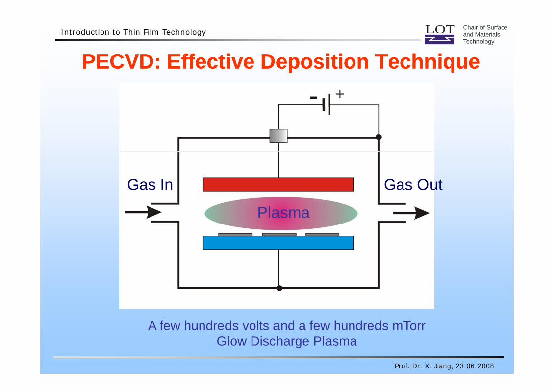
PECVD: Effective Deposition TechniquePECVD: Effective Deposition TechniquePECVD: Effective Deposition TechniquePECVD: Effective Deposition Technique
Gas OutGas In
Plasma
A few hundreds volts and a few hundreds mTorr
Prof. Dr. X. Jiang, 23.06.2008
A few hundreds volts and a few hundreds mTorr Glow Discharge Plasma
LOT Chair of Surfaceand MaterialsTechnology
Introduction to Thin Film Technology
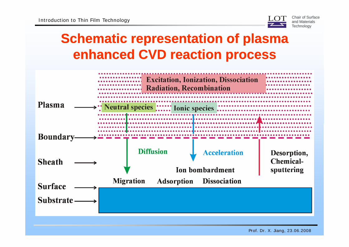
Schematic representation of plasmaSchematic representation of plasmaSchematic representation of plasma Schematic representation of plasma enhanced CVD reaction processenhanced CVD reaction process
Prof. Dr. X. Jiang, 23.06.2008
LOT Chair of Surfaceand MaterialsTechnology
Introduction to Thin Film Technology
Plasma Enhanced CVDPlasma Enhanced CVDPlasma Enhanced CVDPlasma Enhanced CVD
I PlI PlIn Plasma:In Plasma:• Excitation, dissociation and ionization by electron impact. • Excited molecules atoms radicals molecular and/or atomic ionsExcited molecules, atoms, radicals, molecular and/or atomic ions
diffuse to the substrate.• Reactants and the configuration of electrodes and substrate
h ld ti l di t ib ti i ti l d itholder cause a spatial distribution in particle density.• Adsorbed particles migrate in searching for adsorption sites.• Atoms react with each other form clusters thermodynamicallyAtoms react with each other, form clusters, thermodynamically
stable clusters (nuclei)which then expand to films. • Dissociation of molecules during adsorption may also occur. • Bombardments of ions accelerated in the sheath affect surface
reactions.
Prof. Dr. X. Jiang, 23.06.2008

LOT Chair of Surfaceand MaterialsTechnology
Introduction to Thin Film Technology
Reaction Mechanisms
• Complex reaction mechanisms in PE CVD:p
• Cold plasma is not in the thermal equilibrium
• Gases are polyatomic moleculesGases are polyatomic molecules
• Lack of basic data (e.g. reaction cross sections)
• Both processes in the plasma volume and on the substrate• Both processes in the plasma volume and on the substrate contribute to the film formation
Prof. Dr. X. Jiang, 23.06.2008
LOT Chair of Surfaceand MaterialsTechnology
Introduction to Thin Film Technology
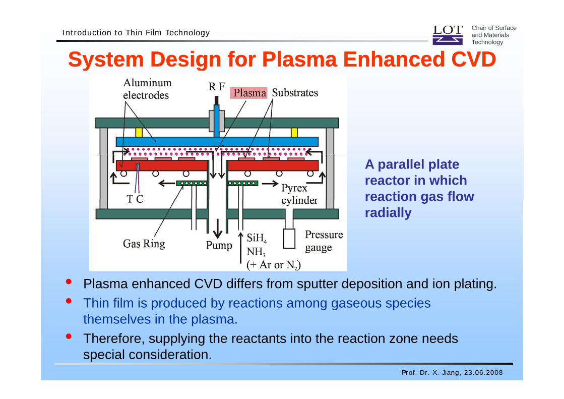
System Design for Plasma Enhanced CVDSystem Design for Plasma Enhanced CVDSystem Design for Plasma Enhanced CVDSystem Design for Plasma Enhanced CVD
A parallel platereactor in which reaction gas flowreaction gas flow radially
• Plasma enhanced CVD differs from sputter deposition and ion plating. p p p g• Thin film is produced by reactions among gaseous species
themselves in the plasma.• Th f l i th t t i t th ti d
Prof. Dr. X. Jiang, 23.06.2008
• Therefore, supplying the reactants into the reaction zone needs special consideration.
LOT Chair of Surfaceand MaterialsTechnology
Introduction to Thin Film Technology
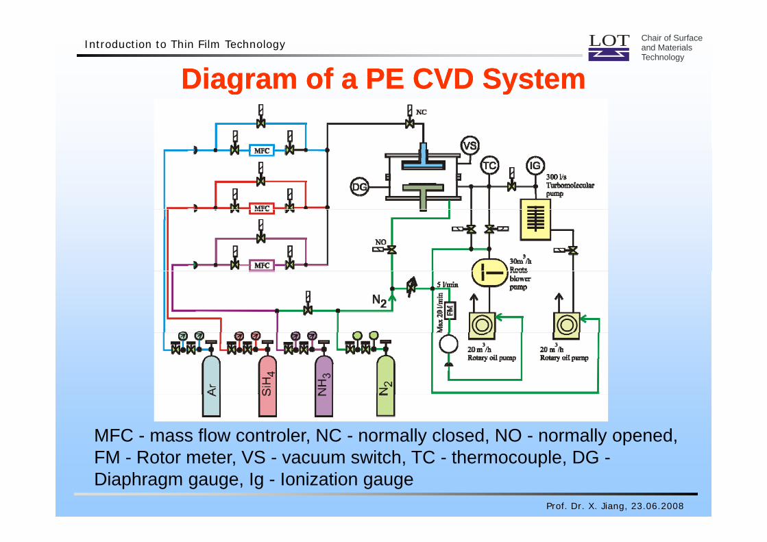
Diagram of a PE CVD SystemDiagram of a PE CVD SystemDiagram of a PE CVD SystemDiagram of a PE CVD System
MFC - mass flow controler, NC - normally closed, NO - normally opened,FM Rotor meter VS vacuum switch TC thermocouple DG
Prof. Dr. X. Jiang, 23.06.2008
FM - Rotor meter, VS - vacuum switch, TC - thermocouple, DG -Diaphragm gauge, Ig - Ionization gauge
LOT Chair of Surfaceand MaterialsTechnology
Introduction to Thin Film Technology
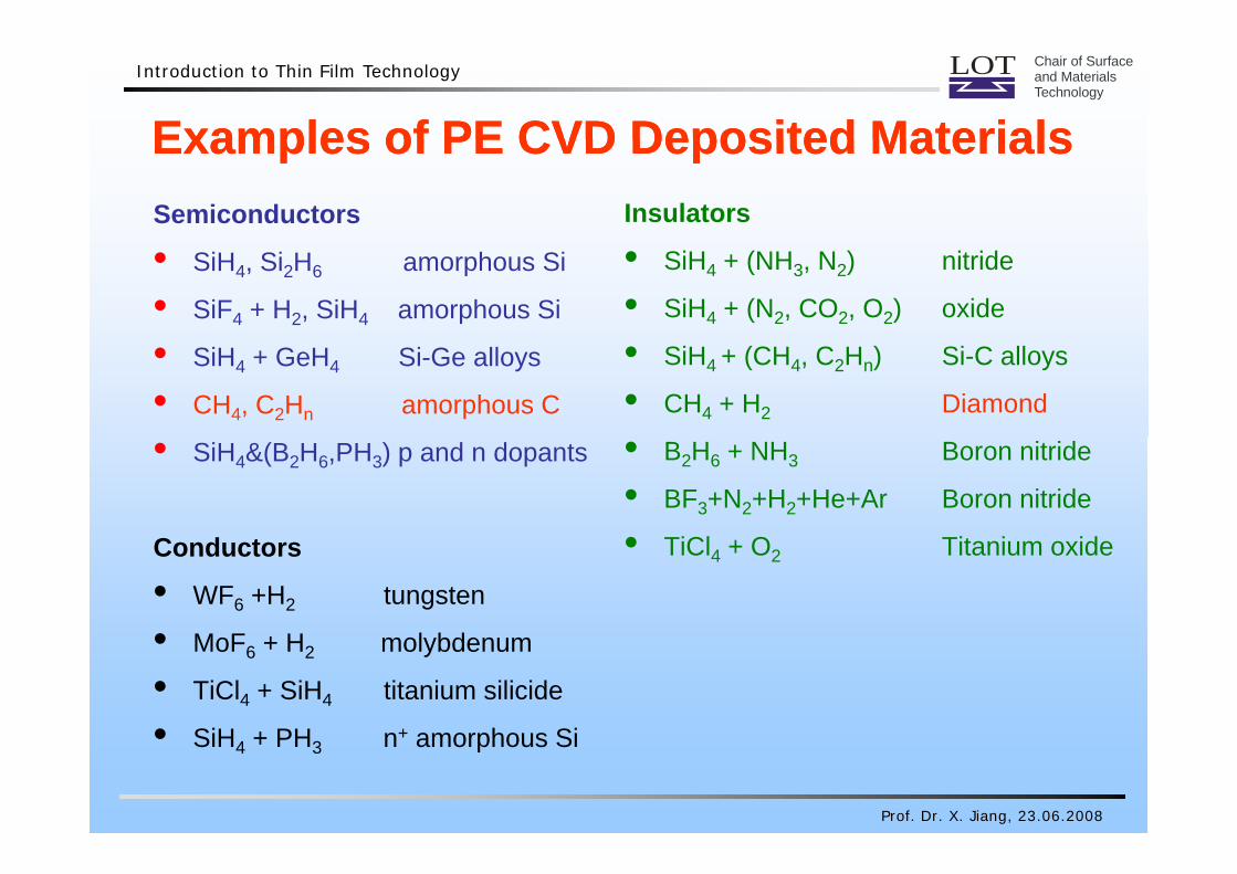
Examples of PE CVD Deposited MaterialsExamples of PE CVD Deposited MaterialsExamples of PE CVD Deposited MaterialsExamples of PE CVD Deposited MaterialsSemiconductors Insulators
• SiH4, Si2H6 amorphous Si
• SiF4 + H2, SiH4 amorphous Si
• SiH4 + (NH3, N2) nitride
• SiH4 + (N2, CO2, O2) oxide
• SiH4 + GeH4 Si-Ge alloys
• CH4, C2Hn amorphous C
• SiH4 + (CH4, C2Hn) Si-C alloys
• CH4 + H2 Diamond
• SiH4&(B2H6,PH3) p and n dopants • B2H6 + NH3 Boron nitride
• BF3+N2+H2+He+Ar Boron nitride
C OConductors
• WF6 +H2 tungsten
• M F H l bd
• TiCl4 + O2 Titanium oxide
• MoF6 + H2 molybdenum
• TiCl4 + SiH4 titanium silicide
• SiH + PH n+ amorphous Si
Prof. Dr. X. Jiang, 23.06.2008
• SiH4 + PH3 n+ amorphous Si

LOT Chair of Surfaceand MaterialsTechnology
Introduction to Thin Film Technology
Applications of Plasma Enhanced CVDApplications of Plasma Enhanced CVDApplications of Plasma Enhanced CVDApplications of Plasma Enhanced CVDICs• Encapsulation for scratch and particle protection of Integrated
Circuits (IC).• I t l l di l t i f ltil l t lli ti t t• Interlevel dielectrics for multilevel metallization structures.• Capacitor dielectrics, diffusion masks, or photolithographic mask
coatings.gOptics• Optical antireflection coatings.• Fabrication of optical waveguide fibers and films.• Production of amorphous silicon and other semiconductor films for
cheap solar cells.cheap solar cells.Electronic and Protective Materials• Important materials: Amorphous silicon, silicon nitride, amorphous
b DLC di d
Prof. Dr. X. Jiang, 23.06.2008
carbon, DLC; diamond
LOT Chair of Surfaceand MaterialsTechnology
Introduction to Thin Film Technology
Surface Modification by Cold PlasmaSurface Modification by Cold PlasmaSurface Modification by Cold PlasmaSurface Modification by Cold Plasma• Carbides and nitrides of transition metals have unique properties• Chemical and thermal stability, hard, often good electrical and
thermal conductors but brittle and difficult to machine• To give metals heat resistance anticorrosion properties or wearTo give metals heat resistance, anticorrosion properties or wear
resistance – modification after machining • Cold plasma – for nitrided or carburized materials at lower
t ttemperatures
Cold plasma have widely been applied toCold plasma have widely been applied to• Surface hardening, making protective or tribological coatings.• Semiconductors: Nitriding and oxidation - important for the
formation of electrically insulating films• Polymers - treating surfaces at low temperature to improve
wettability or adhesion strength
Prof. Dr. X. Jiang, 23.06.2008
wettability or adhesion strength
LOT Chair of Surfaceand MaterialsTechnology
Introduction to Thin Film Technology
I Nit idi d I C b i iI Nit idi d I C b i iIon Nitriding and Ion CarburizingIon Nitriding and Ion Carburizing
• Iron nitrides: ’ Fe N Fe N and ξ Fe N are thermodynamically• Iron nitrides: γ -Fe4N, ε-Fe2-3N, and ξ-Fe2N are thermodynamically unstable.
• Nitriding of the Fe in ambient N2 gas at atmospheric pressure does g 2 g p pnot take place.
• Hard Fe4N layer can be formed by heating iron to ~ 500 oC in NH3.• Salt bath nitriding is an additional technique for surface hardening of
iron and steel.• Cold plasma is advanced nitriding technique for iron and steel used• Cold plasma is advanced nitriding technique for iron and steel used
in industry.
Prof. Dr. X. Jiang, 23.06.2008
LOT Chair of Surfaceand MaterialsTechnology
Introduction to Thin Film Technology
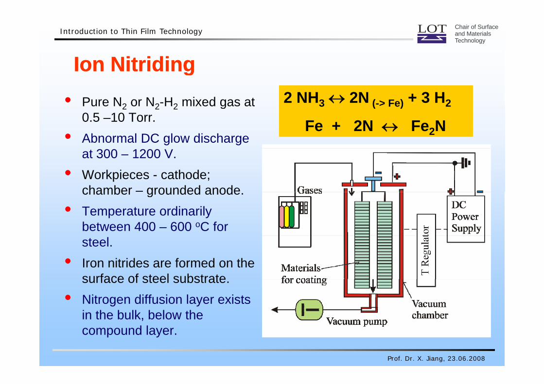
Ion NitridingIon Nitriding• Pure N2 or N2-H2 mixed gas at
Ion NitridingIon Nitriding2 NH3 ↔ 2N (-> Fe) + 3 H2Pure N2 or N2 H2 mixed gas at
0.5 –10 Torr. • Abnormal DC glow discharge
3 ( > Fe) 2
Fe + 2N ↔ Fe2N
at 300 – 1200 V. • Workpieces - cathode;
chamber – grounded anodechamber grounded anode. • Temperature ordinarily
between 400 – 600 oC for steel.
• Iron nitrides are formed on the surface of steel substratesurface of steel substrate.
• Nitrogen diffusion layer exists in the bulk, below the
Prof. Dr. X. Jiang, 23.06.2008
compound layer.
LOT Chair of Surfaceand MaterialsTechnology
Introduction to Thin Film Technology
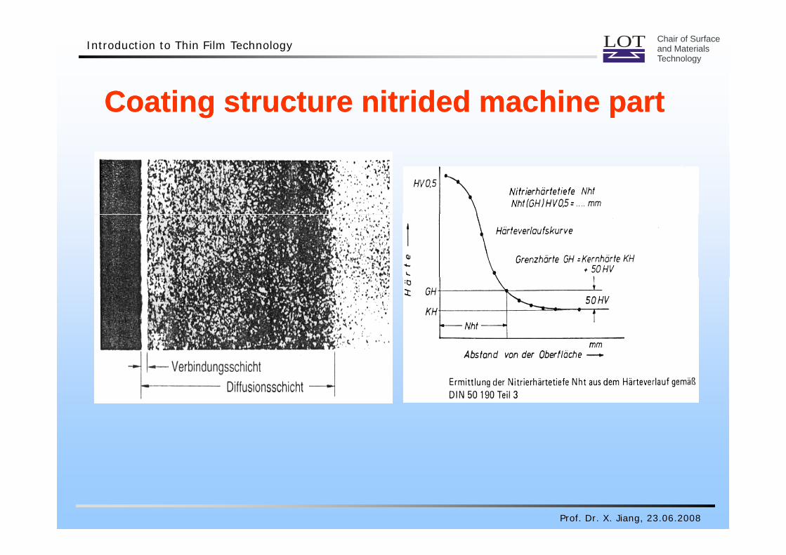
Coating structure nitrided machine partCoating structure nitrided machine part
Prof. Dr. X. Jiang, 23.06.2008
LOT Chair of Surfaceand MaterialsTechnology
Introduction to Thin Film Technology
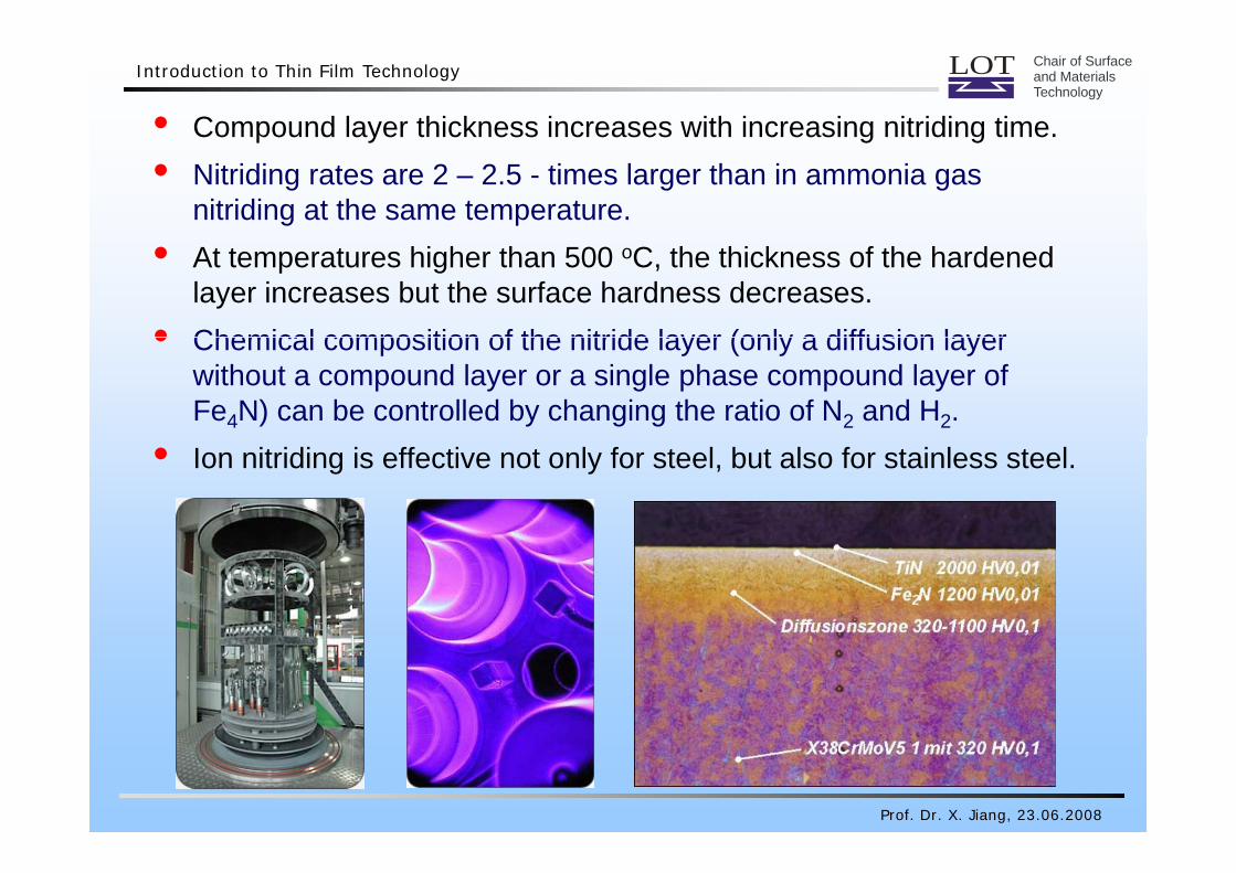
• Compound layer thickness increases with increasing nitriding time. p y g g• Nitriding rates are 2 – 2.5 - times larger than in ammonia gas
nitriding at the same temperature.• At temperatures higher than 500 oC, the thickness of the hardened
layer increases but the surface hardness decreases.• Chemical composition of the nitride layer (only a diffusion layer• Chemical composition of the nitride layer (only a diffusion layer
without a compound layer or a single phase compound layer of Fe4N) can be controlled by changing the ratio of N2 and H2.
• Ion nitriding is effective not only for steel, but also for stainless steel.
Prof. Dr. X. Jiang, 23.06.2008
LOT Chair of Surfaceand MaterialsTechnology
Introduction to Thin Film Technology
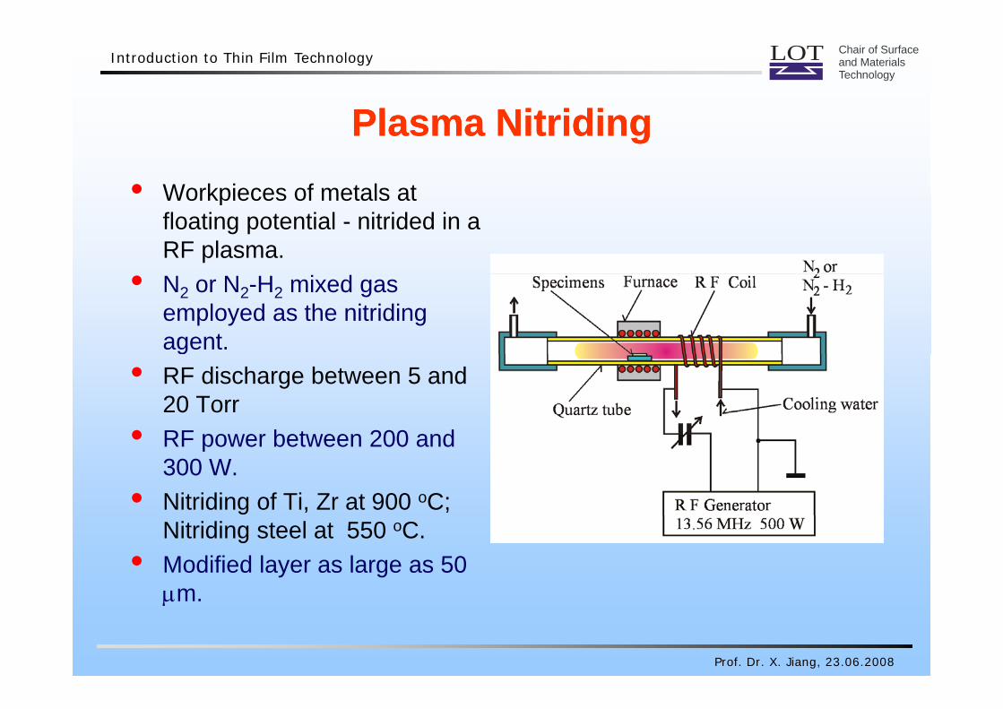
Pl Nit idiPl Nit idiPlasma NitridingPlasma Nitriding• Workpieces of metals atWorkpieces of metals at
floating potential - nitrided in a RF plasma.
• N2 or N2-H2 mixed gas employed as the nitriding agent.
• RF discharge between 5 and 20 Torr
• RF power between 200 and• RF power between 200 and 300 W.
• Nitriding of Ti, Zr at 900 oC; Nitriding steel at 550 oC.
• Modified layer as large as 50 μm
Prof. Dr. X. Jiang, 23.06.2008
μm.

LOT Chair of Surfaceand MaterialsTechnology
Introduction to Thin Film Technology
P l Pl ® i i i V bi d hi h bild
PulsPlasma®_Nitrieranlage PP 300 ø 2000 x 3200
Zahnkranz, 42 CrMo 4
PulsPlasma®nitriert - mit Verbindungsschichtbildung
Prof. Dr. X. Jiang, 23.06.2008

LOT Chair of Surfaceand MaterialsTechnology
Introduction to Thin Film Technology
Plasma Oxidation and Plasma AnodizationPlasma Oxidation and Plasma Anodization
• Surface oxidation of materials at a floating potential in a cold plasma i ll d l id tiis called plasma oxidation
• Plasma oxidation for materials at positively bias potential is calledplasma anodizationplasma anodization
• Plasma anodization is employed for obtaining a thick oxide layer• Both techniques provide dense oxide films on solid material surfaces q p
at < 300 oC • High oxidation rate can be achieved by plasma anodization• Oxide film thickness and oxidation rate can be controlled by bias
voltage and /or current
Prof. Dr. X. Jiang, 23.06.2008
LOT Chair of Surfaceand MaterialsTechnology
Introduction to Thin Film Technology
• These techniques have been applied for the formation of electricallyinsulating films on either metals and semiconductors surfaces (Al, Si,Nb, GaAs, InP).Nb, GaAs, InP).
• Disadvantages of conventional high temperature oxidation: (for Si):oxidation-induced staking faults, excessive diffusion of dopants,
ti f l t (f I P G A ) h A d P d ievaporation of elements (from InP, GaAs) such as As, and P duringoxidation.
• Low temperature plasma processing is an alternativeLow temperature plasma processing is an alternative.• Good insulating pinhole free films with high breakdown voltages, can
be formed at low temperatures on semiconductors.• In high temperature superconducting oxides, plasma oxidation
techniques are applied to improve the oxygen incorporation.
Prof. Dr. X. Jiang, 23.06.2008

LOT Chair of Surfaceand MaterialsTechnology
Introduction to Thin Film Technology
Hydrogen Neutralization in SemiconductorsHydrogen Neutralization in Semiconductors
• Interest in the effect of hydrogen plasma exposure on properties ofInterest in the effect of hydrogen plasma exposure on properties of semiconductors.
• Hydrogen passivates deep level defects in semiconductors and improves the performance of electronic devices.
• Numerous types of plasma systems (RF, microwave discharges) have been used for hydrogen plasma exposurebeen used for hydrogen plasma exposure.
• Sample which is normally placed at floating potential: directly immersed in the plasma or immersed in the downstream afterglow.
• The depth of passivation shows characteristic diffusion limited t1/2
dependence - sample temperatures: 100 – 350 oC to permit diffusion of hydrogenhydrogen.
• Pure hydrogen plasma• Small amounts of (0 1 0 3 %) of H O or O can be added into an
Prof. Dr. X. Jiang, 23.06.2008
Small amounts of (0.1 – 0.3 %) of H2O or O2 can be added into an hydrogen plasma.
LOT Chair of Surfaceand MaterialsTechnology
Introduction to Thin Film Technology
• Oxygen addition drastically increases the steady-state H atomOxygen addition drastically increases the steady state H atom concentration and oxygen does not diffuse into Si under conditions of shallow impurity passivation.
• Hydrogenation of InP shows very significant surface degradation due to P loss and subsequent In droplet formation.
• It is necessary to provide a simultaneous P overpressure or toIt is necessary to provide a simultaneous P overpressure, or to protect the InP surface with a thin H permeable cap layer.
Prof. Dr. X. Jiang, 23.06.2008