Embed Size (px)
Citation preview

Introduction to Engineering Materials
ENGR2000
Chapter 4: Imperfections in Solids
Dr. Coates

Learning Objectives
1. Describe both vacancy and self interstitial defects
2. Calculate the equilibrium number of vacancies in
a material at some specified temperature
3. Name the two types of solid solutions, provide a
brief written definition and/or sketch
4. Given the mass and atomic weights of two or
more elements in a metal alloy, calculate the
weight percent or atom percent of each element

The structure of a material
- arrangement of its internal components
• Subatomic structure
– Electrons & nuclei within the individual atoms
• Atomic structure
– Atoms & molecules within the material
• Microscopic structure
– Large groups of atoms aggregated together
• Macroscopic structure
– Elements that may be viewed with the naked eye

4.1 Introduction
• Imperfections or defects in crystal structures
– ‘mistakes’ in atomic arrangement
– single atoms (point defects)
– rows of atoms (linear defects)
– planes of atoms (planar defects)
– 3D clusters of atoms (volume defects)

5
• Vacancies:-vacant atomic sites in a structure.
• Self-Interstitials:-"extra" atoms positioned between atomic sites.
Point Defects in Metals
Vacancy
distortion
of planes
self-interstitial
distortion of planes

4.2 Vacancies and Self-Interstitials
• Self-interstitials in metals
– Atom from the crystal is crowded into an interstitial site
• Introduces relatively large distortions Why?
• How probable would you expect this to be?
Which is more likely a self interstitial site
or a vacancy? Why?

7
Boltzmann's constant
(1.38 x 10⁻²³
J/atom-K)
(8.62 x 10⁻⁵
eV/atom-K)
Nv
N= exp
Qv
kT
No. of defects
No. of potential defect sites
Activation energy
Temperature
Each lattice site is a potential vacancy site
• Equilibrium concentration varies with temperature!
Equilibrium Concentration:
Point Defects

8
• We can get Qv from
an experiment.
Nv
N= exp
- Qv
kT
Measuring Activation Energy
• Measure this...
Nv
N
T
exponential dependence!
defect concentration
• Replot it...
1/T
N
Nvln
-Qv /k
slope

Example 4.1
• Calculate the equilibrium number of vacancies per
cubic meter for Cu at 1000 0C. The energy for
vacancy formation is 0.9 eV/atom; the atomic
weight and density for Cu are 63.5 g/mol and 8.4
g/cm3, respectively.

325
3
28
328
3
/102.2
12731062.8
9.0exp108
exp
/100.8
:..
/4.8,/5.63,/9.0,1273
mvacancies
KK
eV
eV
m
atoms
kT
QNN
:mpervacancies of
NmatomsA
N
V
n
volumeunitpereim per sitesatomic of #
cmgmolgAatomeVQKT
:Given
5-
vv
3
Cu
A
3
Cuv

4.3 Impurities in Solids
• Alloys
– Impurity atoms added intentionally to impart specific
characteristics to metals
• Solid solutions
– Solute or impurities
– Solvent or host material

Solid Solutions
• Solid solutions are formed when…
– Solute atoms are added to the solvent
– Crystal structure is maintained
– No new structures are formed
They are compositionally homogenous? How so?
Impurity atoms are randomly and uniformly dispersed within solid

Substitutional solid solutions
• Solute or impurity atoms substitute for the solvent
or host atoms.

Hume-Rothery Rules
• Factors that determine the degree to which the
solute dissolves in the solvent
1. Atomic size – difference in atomic radii must be less
than ~15%.
2. Crystal structure – same for metals of both atom
types.
3. Electro negativity->larger the difference -> more
likelihood they will form an intermetallic compound
instead of a substitutional solid solution.
4. Valences – other factors being equal, a metal of lower
valency has more of a tendency to dissolve another
metal of higher valency than vice versa

Substitutional solid solutions
• Cu & Ni solution
– Atomic radii for Cu & Ni are 0.128 nm & 0.125 nm.
– Both have FCC crystal structure
– EN values are 1.9 & 1.8
– Valences are +1 & +2.

Interstitial solid solutions
• Solute or impurity atoms fill the interstices or
voids among the solvent or host atoms.

Interstitial solid solutions
How do you think the atomic radii of a solute
compares to that of the solvent for interstitial solid
solutions?
• C in Fe
– Atomic radii of C & Fe are 0.071 nm & 0.124 nm.
– Max. concentration of C is ~2 %.

Cool video of the day
https://www.youtube.com/watch?v
=urq8SuPMZ_w

Impurities in Solids• Specification of composition
– weight percent 100x 21
11
mm
mC
m1 = mass of component 1
100x 21
1'
1
mm
m
nn
nC
nm1 = number of moles of component 1
– atom percent
How is nm related to mass, m1 and atomic weight,
A1 of an element?1
11
A
mnm

Composition Conversions
bACAC
ACC
aACAC
ACC
bACAC
ACC
aACAC
ACC
7.4100
7.4100
6.4100
6.4100
:ionsconcentrat theof in terms alloys of weightsatomic &Density
1
'
12
'
2
2
'
22
1
'
12
'
2
1
'
11
1221
12'
2
1221
21'
1

Composition Conversions
11.4100
10.4100
2
2
1
1
2
2
1
1
A
C
A
CA
CC
ave
ave
bCC
CC
aCC
CC
9.410
9.410
3
2
2
1
1
2"2
3
2
2
1
1
1"1
Average composition density and atomic weight
Conversion of weight percent to mass per unit volume

Linear Defects
4.5 Dislocations
• Dislocation
– A 1D defect around which some of the atoms are
misaligned.
– Edge dislocation
– Screw dislocation
– Mixed dislocation

23
• are line defects,
• slip between crystal planes result when dislocations move,
• produce permanent (plastic) deformation.
Dislocations:
Schematic of Zinc (HCP):
• before deformation • after tensile elongation
slip steps
Line Defects

Edge Dislocation
• A linear defect that centers around the line
(dislocation line) that is defined along the end of
the extra half-plane of atoms.
Magnitude and direction of lattice
distortion represented by Burgers
vector
Extra half plane

Edge Dislocation
• Linear defect
• Centered on line that is defined along the end of
the extra half plane of atoms (dislocation line)
• Atoms above
dislocation line are
squeezed together
or pulled apart?
Below dislocation line?

Screw Dislocation
• Formed by applied shear stress
• Upper front region of crystal shifted by one atomic
distance to the right
• Burger’s vector is parallel to the unit tangent
vector
• Linear and along a dislocation line
tb
//

Screw Dislocation

Mixed Dislocation• Neither pure edge or pure screw dislocation

TEM Image of Dislocations

Planar Defects
4.6 Interfacial Defects
• 2D boundaries that separate regions of materials
with different crystal structures and/or
crystallographic orientations
– External surfaces
– Grain boundaries
– Twin boundaries
– Stacking faults
– Phase boundaries

External Surfaces
• Surface along which the crystal structure
terminates.
• Surface atoms are not bonded to the maximum
number of nearest neighbors, hence are in a higher
energy state than interior atoms.
– Surface energy or surface tension

Grain Boundaries
• Boundary separating crystals with different
orientations.

Grain Boundaries

Grain Boundaries
• Atoms bonded less regularly along grain boundary
results in an interfacial or grain boundary energy!
• How might grain boundary energy
– be related to the magnitude of angle between
boundaries (proportional/inversely proportional)?
– influence chemically reactivity
– Be related to size of grains?
– Impurity atomic presence?
– Temperature?

Tilt Boundary
• Small angle grain boundary.
• An ordered arrangement of
edge dislocations.
tb

Twist Boundary
• Angle of misorientation is parallel to the boundary
• An ordered arrangement of screw dislocations.
tb
//

Phase Boundaries
• A phase is defined as a homogenous portion of a
system that has uniform physical and chemical
characteristics (Section 9.3)
• Exist in multiphase materials wherein a different
phase exists on each side of the boundary
• Each of the constituent phases has its own
distinctive physical or chemical characteristics

Twin Boundary
• A mirror image of the crystal structure across a
boundary.
– formed during plastic deformation from shear forces
(mechanical twins)
– formed during rapid cooling from high temperatures
(annealing twins)
Occurs on a definite
crystallographic plane and in a
specific direction!

Miscellaneous Interfacial Defects
• Stacking faults
– Interruption in stacking sequence of close packed
planes ex. ABCABCABC for the FCC
• Ferromagnetic domain walls
– boundaries have different directions of magnetization

Volume Defects
4.7 Bulk Defects
• Normally introduced during processing and
fabrication
– Pores
– Cracks
– Foreign inclusions
– Other phases

Example
Classify each of the following defects as point,linear, planar or volume defects:
(a) A screw dislocation
(b) A low-angle twist boundary composed of screwdislocations
(c) A vacancy
(d) A spherical cluster of 50 vacancies
(e) A local region of atoms with a BCC structure withinan FCC lattice
(f) The boundary between the above BCC & FCC regions
linear
planar
pointvolume
volume
planar
4.8 Atomic Vibrations
- as imperfections or defects
• Atoms in a solid material are vibrating about their
lattice positions
• Not all atoms vibrate at the same frequency &
amplitude or energy
• How does temperature relate to the vibrational
activity of atoms and molecules?

4.8 Atomic Vibrations
- effect on properties of the material
• Temperature
– Measure of the average vibrational activity of atoms
and molecules
• Melting of a solid
– Occurs when the vibrations are vigorous enough to
rupture large numbers of atomic bonds

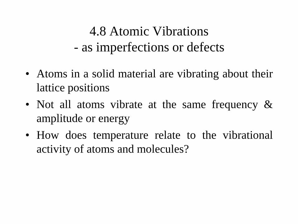
Optical Microscopy
• Use of a light microscope (upper limit x2000)
– For opague materials, only the surface is subjected to
observation
– Used in a reflecting mode, contrasts in image result
from differences in reflectivity of the various regions
– Investigations are often termed metallographic
• Surface preparation
– grounded and polished (finer abrasive papers and
powders)
– Chemically treated (etching)

Microscopic Examination
Microscopic Examination

Optical Microscopy
•Small grooves form along grain boundaries as a result of etching
•Luster of each grain depends on its reflective properties

Electron Microscopy
• Image formed using beams of electrons
• Electrons accelerated across large voltages
resulting in short wavelengths
• Electrons focused and image formed with
magnetic lenses

Electron Microscopy
• Transmission Electron Microscopy (TEM)
– Contrasts produced by beam scattering or diffraction
– Thin foil form, why?
– 1,000,000 x
• Scanning Electron Microscopy (SEM)
– Reflected beams
– Image displayed on a cathode ray tube (TV)
– 50,000x
• Scanning Probe Microscopy (SPM)
– Does not use light or electrons to generate image
– Probe generates topographical map on an atomic scale
– 109x

4.11 Grain Size Determination
• Mean Intercept Length:
• Comparison method: American Society for
Testing and Materials (ASTM) grain size number
G …
• Does grain size # increase or decrease with
decreasing grain size? Why?
number sizegrainG
100 of ionmagnificat a at /ingrains of #nn G
21 ,2
tionserofP
lengthlinetotalL
ionmagnificatMPM
L
T
T
secint#
,
,

Grain Size Determination
• Fine grained material
– ASTM grain size 8 - 10
• Coarse grained material
– ASTM grain size 2 - 3

Example
• Assuming grains have a square shape, estimate the
average grain size in microns of a material whose
ASTM grain size numbers are 2 and 8 for two
different conditions.

mdmd
mDmD
cmmincmininD
inD
inD
N
inD
D
inD
ASTMASTM
ASTMASTM
nn
n
n
4.22and180
: Table From
5.22and180
:numbers ASTM twoFor the
/10/54.2100
2
100
2
2
/grains of #1
2
100xat of areaan occupiesgrain 1
100xD 100x at length Edge
of areaan occupiesgrain 1
D square oflength Edge
8#2#
8#2#
42/12/1
2/1100
2
2100
1
22100
100
22

Design Problem 4.D1
• Al-Li alloys have been developed by the aircraft
industry in order to reduce the weight and improve
performance. A commercial aircraft skin material
having a density of 2.55 g/cm3 is desired.
Compute the concentration of Li in wt.% that is
required.

Design Problem 4.D2
• Copper (Cu) and platinum (Pt) both have the FCC
crystal structure, and Cu forms a substitutional
solid solution for concentrations up to
approximately 6 wt% Cu at room temperature.
Determine the concentration in weight percent of
Cu that must be added to Pt to yield a unit cell
edge length of 0.390 nm.


![· Mr Shaun Cameron, Mrs Joan Golda Cameron and Cameron Farms Pty Ltd [ACN 008 707 926] (Mr and Mrs Cameron are the principals of Cameron Farms Pty Ltd ("Camerons") It is my understanding](https://img.dokumen.tips/doc/110x75/5e0b63e15dd8b42d0531a5fd/mr-shaun-cameron-mrs-joan-golda-cameron-and-cameron-farms-pty-ltd-acn-008-707.jpg)