Embed Size (px)
Citation preview
ECE1371 Advanced Analog Circuits
INTRODUCTION TODELTA-SIGMA ADCS
Richard [email protected]
ECE1371 2
NLCOTD: Level TranslatorVDD1 > VDD2, e.g.
• VDD1 < VDD2, e.g.
• Constraints: CMOS1-V and 3-V devicesno static current
3-V logic 1-V logic?
1-V logic 3-V logic?
ECE1371 3
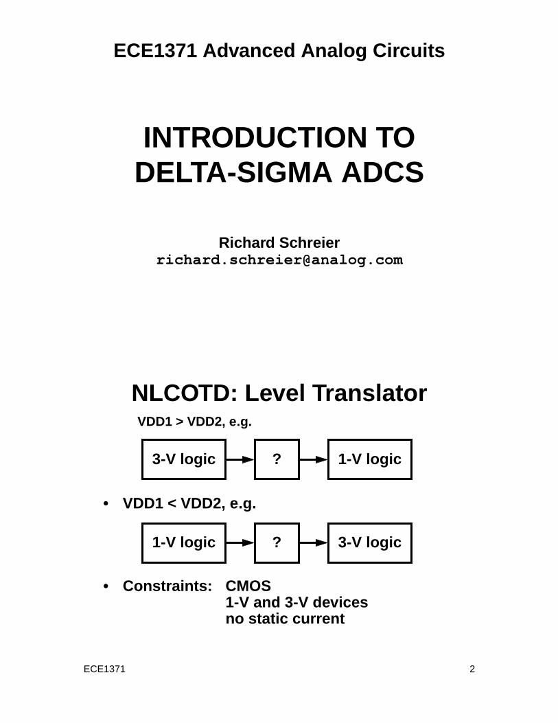
Highlights(i.e. What you will learn today)
1 1st-order modulator (MOD1)Structure and theory of operation
2 Inherent linearity of binary modulators
3 Inherent anti-aliasing of continuous-timemodulators
4 2nd-order modulator (MOD2)
5 Good FFT practice
ECE1371 4
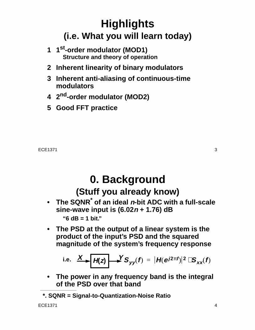
0. Background(Stuff you already know)
• The SQNR* of an ideal n-bit ADC with a full-scalesine-wave input is (6.02 n + 1.76) dB
“6 dB = 1 bit.”
• The PSD at the output of a linear system is theproduct of the input’s PSD and the squaredmagnitude of the system’s frequency response
i.e.
• The power in any frequency band is the integralof the PSD over that band
*. SQNR = Signal-to-Quantization-Noise Ratio
H(z)X YSyy f( ) H ej 2πf( ) 2 Sxx f( )⋅=
ECE1371 5
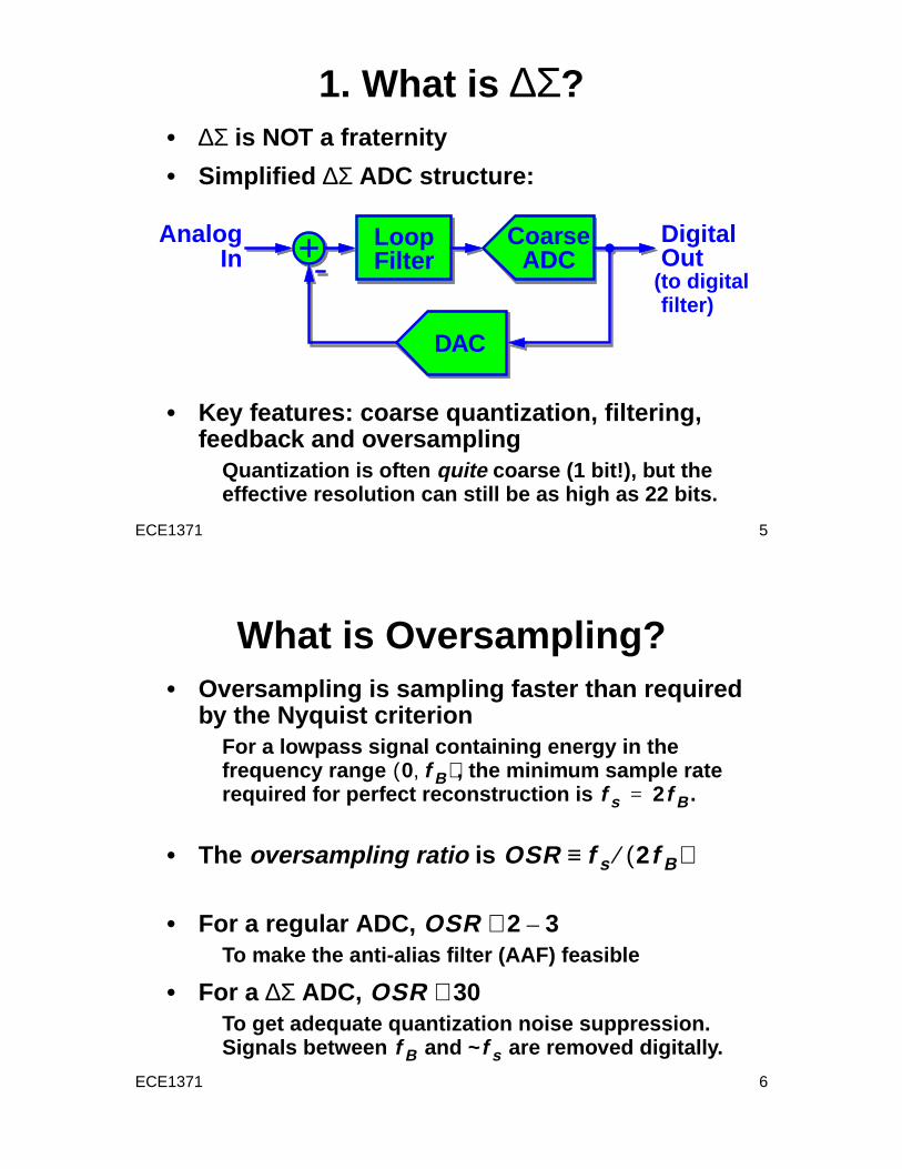
1. What is ∆Σ?• ∆Σ is NOT a fraternity
• Simplified ∆Σ ADC structure:
• Key features: coarse quantization, filtering,feedback and oversampling
Quantization is often quite coarse (1 bit!), but theeffective resolution can still be as high as 22 bits.
LoopFilter
CoarseADC
DAC
LoopFilter
CoarseADC
DAC
AnalogIn
DigitalOut
(to digitalfilter)
ECE1371 6
What is Oversampling?• Oversampling is sampling faster than required
by the Nyquist criterionFor a lowpass signal containing energy in thefrequency range , the minimum sample raterequired for perfect reconstruction is .
• The oversampling ratio is
• For a regular ADC,To make the anti-alias filter (AAF) feasible
• For a ∆Σ ADC,To get adequate quantization noise suppression.Signals between and ~ are removed digitally.
0 f B,( )f s 2f B=
OSR f s 2f B( )⁄≡
OSR 2 3–∼
OSR 30∼
f B f s

ECE1371 7
Oversampling Simplifies AAF
f s 2⁄
DesiredSignal
UndesiredSignals
f
OSR ~ 1:
First alias band is very close
f s 2⁄f
OSR = 3: Wide transition band
Alias far away
ECE1371 8
How Does A ∆Σ ADC Work?• Coarse quantization ⇒ lots of quantization error.
So how can a ∆Σ ADC achieve 22-bit resolution?
• A ∆Σ ADC spectrally separates the quantizationerror from the signal through noise-shaping
∆ΣADC
u v DecimationFilter
analog1 bit @fs
digitaloutput
desiredshaped
n@2fB
Nyquist-ratePCM Data
1
–1t
noise
winput
t
f s 2⁄f B f s 2⁄f B f B
undesiredsignals
signal
ECE1371 9
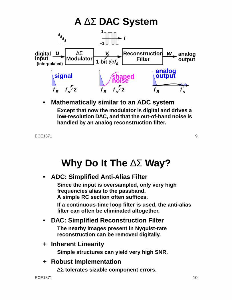
A ∆Σ DAC System
• Mathematically similar to an ADC systemExcept that now the modulator is digital and drives alow-resolution DAC, and that the out-of-band noise ishandled by an analog reconstruction filter.
∆ΣModulator
u v ReconstructionFilter
digital
1 bit @fs
analogoutput
signal shapedanalogoutput
1
–1t
noise
inputw
(interpolated)
f B f s 2⁄ f B f s 2⁄ f B f s
ECE1371 10
Why Do It The ∆Σ Way?• ADC: Simplified Anti-Alias Filter
Since the input is oversampled, only very highfrequencies alias to the passband.A simple RC section often suffices.If a continuous-time loop filter is used, the anti-aliasfilter can often be eliminated altogether.
• DAC: Simplified Reconstruction FilterThe nearby images present in Nyquist-ratereconstruction can be removed digitally.
+ Inherent LinearitySimple structures can yield very high SNR.
+ Robust Implementation∆Σ tolerates sizable component errors.

ECE1371 11
2. MOD1: 1st-Order ∆Σ Modulator[Ch. 2 of Schreier & Temes]
z-1
z-1
QU VY
Quantizer
DAC
(1-bit)
FeedbackDAC
v
y
v’
v
V’
“ ∆” “ Σ”1
–1
Since two points define a line,a binary DAC is inherentl y linear.
ECE1371 12
MOD1 Analysis• Exact analysis is intractable for all but the
simplest inputs, so treat the quantizer as anadditive noise source:
z-1
z-1
Q
Y V
E
⇒(1–z-1) V(z) = U(z) – z-1V(z) + (1–z-1)E(z)
U VY
V(z) = Y(z) + E(z)Y(z) = ( U(z) – z-1V(z) ) / (1–z-1)
V(z) = U(z) + (1–z–1)E(z)

ECE1371 13
The Noise Transfer Function (NTF)• In general, V(z) = STF(z)•U(z) + NTF(z)•E(z)
• For MOD1, NTF(z) = 1–z–1
The quantization noise has spectral shape!
• The total noise power increases, but the noisepower at low frequencies is reduced
0 0.1 0.2 0.3 0.4 0.50
1
2
3
4NTF ej 2πf( ) 2
Normalized Frequency ( f /fs)
ω2 for ω 1«≅
Poles & zeros:
ECE1371 14
In-band Quant. Noise Power• Assume that e is white with power
i.e.• The in-band quantization noise power is
• Since ,
• For MOD1, an octave increase in OSR increasesSQNR by 9 dB
“1.5-bit/octave SQNR-OSR trade-off.”
σe2
See ω( ) σe2 π⁄=
IQNP H ejω( ) 2See ω( )dω
0
ωB
∫=σe
2
π------ ω2dω
0
ωB
∫≅
OSR πωB-------≡ IQNP
π2σe2
3------------- OSR( ) 3–=
ECE1371 15
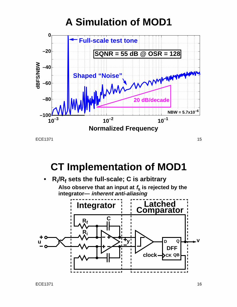
A Simulation of MOD1
10–3 10–2 10–1–100
–80
–60
–40
–20
0
Normalized Frequency
20 dB/decade
SQNR = 55 dB @ OSR = 128
NBW = 5.7x10⁻⁶
Full-scale test tone
Shaped “Noise”
dBF
S/N
BW
ECE1371 16
CT Implementation of MOD1• Ri/Rf sets the full-scale; C is arbitrary
Also observe that an input at fs is rejected by theintegrator— inherent anti-aliasing
LatchedIntegrator
CK
D Q
DFFclock QB
yu
C
Ri
Rf
v
Comparator

ECE1371 17
MOD1-CT Waveforms
• With u=0, v alternates between +1 and –1
• With u>0, y drifts upwards; v containsconsecutive +1s to counteract this drift
0 5 10 15 200 5 10 15 20
0
u = 0
v
y
u = 0.06
Time Time
–1
1
0
v
y
–1
1
ECE1371 18
MOD1-CT STF =Recall
1 z 1––s
-----------------z es=
Pole-zero cancellation@ s = 0
Zeros @ s = 2k πi
s-plane ω
σ
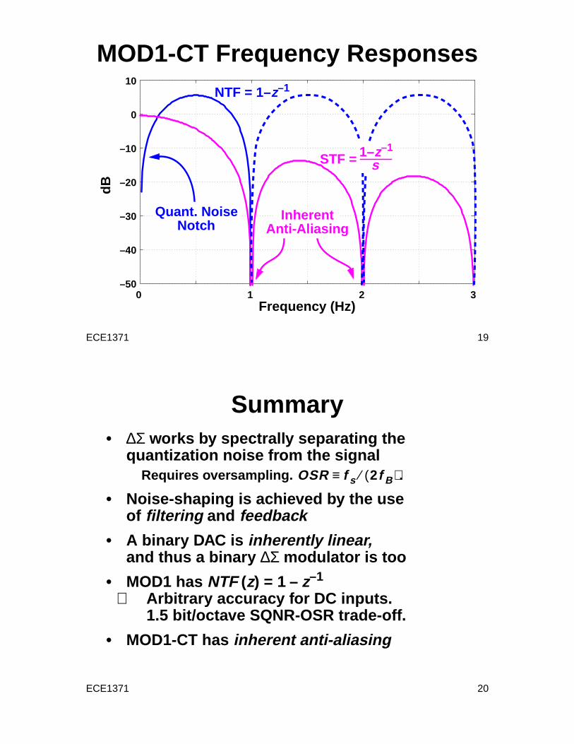
ECE1371 19
MOD1-CT Frequency Responses
0 1 2 3–50
–40
–30
–20
–10
0
10
Frequency (Hz)
dB
InherentAnti-Aliasing
Quant. NoiseNotch
NTF = 1–z–1
STF = 1–z–1
s
ECE1371 20
Summary• ∆Σ works by spectrally separating the
quantization noise from the signalRequires oversampling. .
• Noise-shaping is achieved by the useof filtering and feedback
• A binary DAC is inherently linear,and thus a binary ∆Σ modulator is too
• MOD1 has NTF (z) = 1 – z–1
⇒ Arbitrary accuracy for DC inputs.1.5 bit/octave SQNR-OSR trade-off.
• MOD1-CT has inherent anti-aliasing
OSR f s 2f B( )⁄≡
ECE1371 21
NLCOTD
3V → 1V:3V
1V
3V
3V
1V → 3V:
1V
3V
3V
3V
3V
ECE1371 22
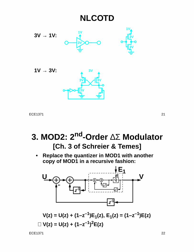
3. MOD2: 2nd-Order ∆Σ Modulator[Ch. 3 of Schreier & Temes]
• Replace the quantizer in MOD1 with anothercopy of MOD1 in a recursive fashion:
V(z) = U(z) + (1–z–1)E1(z), E1(z) = (1–z–1)E(z)
⇒V(z) = U(z) + (1–z–1)2E(z)
z-1
Q
z-1
z-1
z-1
U VE1
E
ECE1371 23
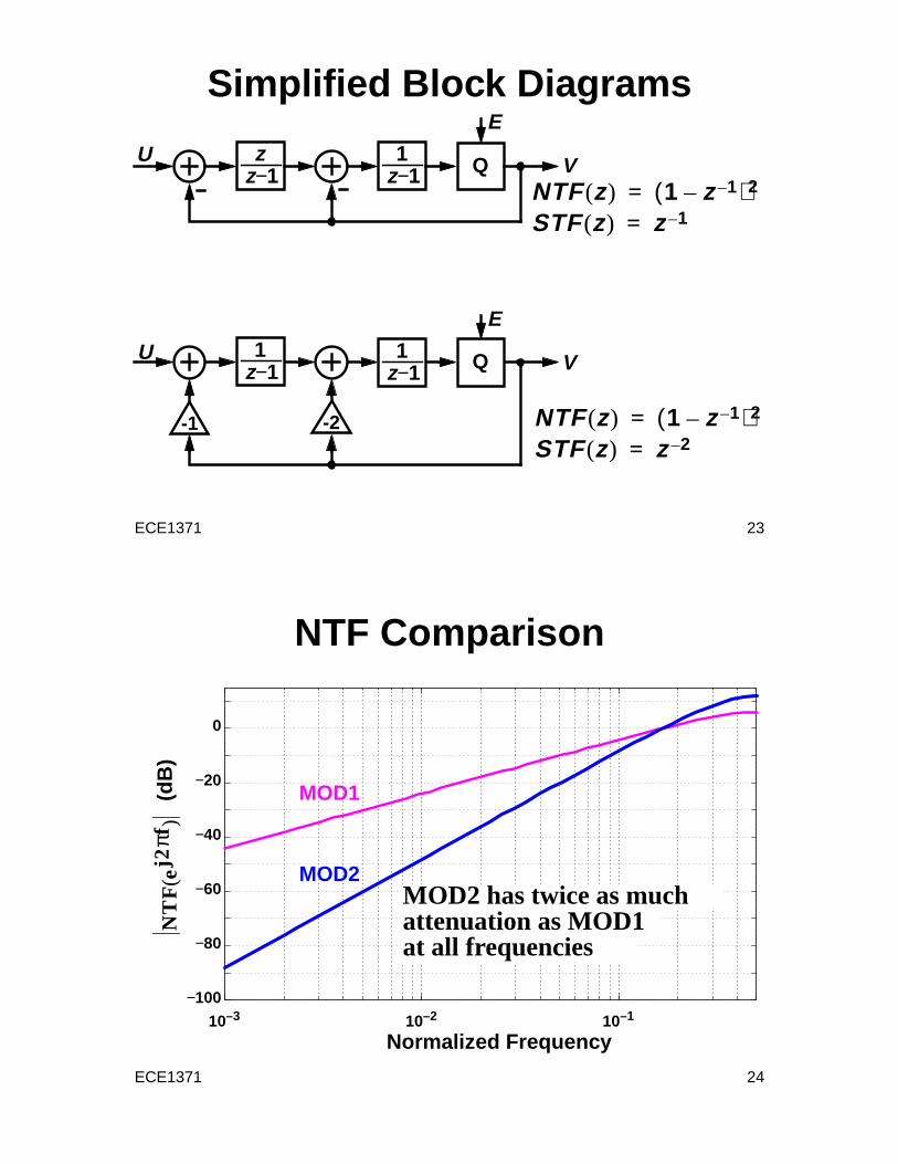
Simplified Block Diagrams
Q1z−1
zz−1
U V
E
NTF z( ) 1 z 1––( )2=STF z( ) z 1–=
Q1z−1
1z−1
U V
E
-2-1 NTF z( ) 1 z 1––( )2=STF z( ) z 2–=
ECE1371 24
NTF Comparison
10–3 10–2 10–1−100
−80
−60
−40
−20
0
NT
Fe
j2πf
()
(dB
)
Normalized Frequency
MOD1
MOD2MOD2 has twice as muchattenuation as MOD1at all frequencies

ECE1371 25
In-band Quant. Noise Power• For MOD2,
• As before, and
• So now
With binary quantization to ±1, and thus .
• “An octave increase in OSR increases MOD2’sSQNR by 15 dB (2.5 bits)”
H e jω( ) 2 ω4≈
IQNP H ejω( ) 2See ω( )dω0
ωB∫=
See ω( ) σe2 π⁄=
IQNPπ4σe
2
5------------- OSR( ) 5–=
∆ 2= σe2 ∆2 12⁄ 1 3⁄= =
ECE1371 26
Simulation ExampleInput at 75% of FullScale
0 50 100 150 200–1
0
1
Sample number
ECE1371 27
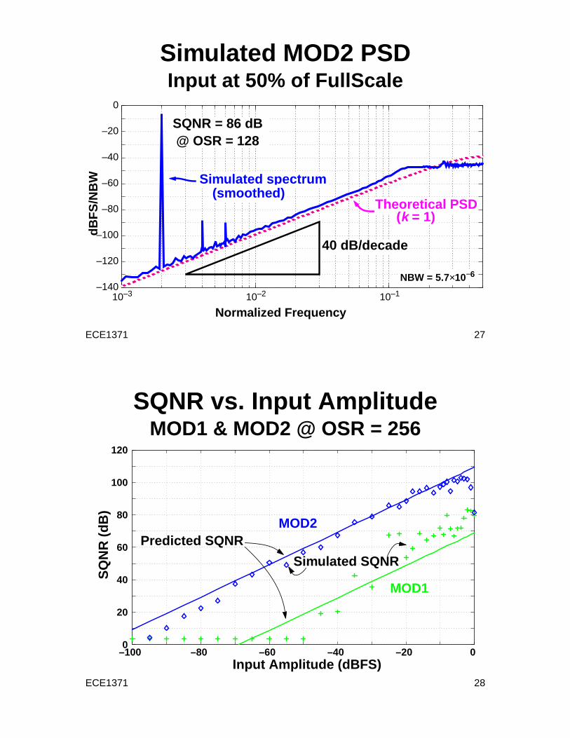
Simulated MOD2 PSDInput at 50% of FullScale
10–3 10–2 10–1–140
–120
–100
–80
–60
–40
–20
0
SQNR = 86 dB@ OSR = 128
40 dB/decade
Theoretical PSD(k = 1)
Simulated spectrum
Normalized Frequency
dBF
S/N
BW
(smoothed)
NBW = 5.7×10⁻⁶
ECE1371 28
SQNR vs. Input AmplitudeMOD1 & MOD2 @ OSR = 256
–100 –80 –60 –40 –20 00
20
40
60
80
100
120
Input Amplitude (dBFS)
SQ
NR
(dB
)
MOD1
MOD2Predicted SQNR
Simulated SQNR
ECE1371 29
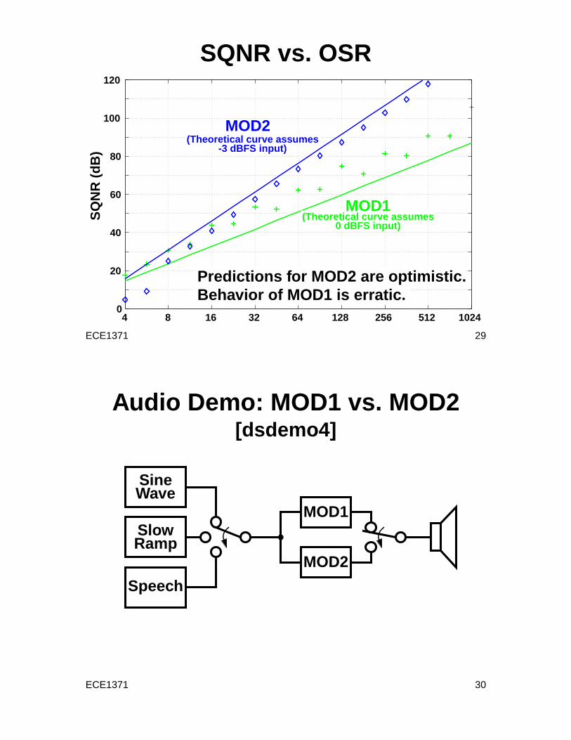
SQNR vs. OSR
4 8 16 32 64 128 256 512 10240
20
40
60
80
100
120
SQ
NR
(dB
)
(Theoretical curve assumes-3 dBFS input)
(Theoretical curve assumes0 dBFS input)
MOD1
MOD2
Predictions for MOD2 are optimistic.Behavior of MOD1 is erratic.
ECE1371 30
Audio Demo: MOD1 vs. MOD2[dsdemo4]
MOD1
MOD2
SineWave
SlowRamp
Speech
ECE1371 31
MOD1 + MOD2 Summary• ∆Σ ADCs rely on filtering and feedback to
achieve high SNR despite coarse quantizationThey also rely on digital signal processing.∆Σ ADCs need to be followed by a digital decimationfilter and ∆Σ DACs need to be preceded by a digitalinterpolation filter.
• Oversampling eases analog filteringrequirements
Anti-alias filter in an ADC; image filter in a DAC.
• Binary quantization yields inherent linearity
• MOD2 is better than MOD115 dB/octave vs. 9 dB/octave SQNR-OSR trade-off.Quantization noise more white.Higher-order modulators are even better.
ECE1371 32
4. Good FFT Practice[Appendix A of Schreier & Temes]
• Use coherent samplingI.e. have an integer number of cycles in the record.
• Use windowingA Hann windowworks well.
• Use enough pointsRecommend .
• Scale (and smooth) the spectrumA full-scale sine wave should yield a 0-dBFS peak.
• State the noise bandwidthFor a Hann window, .
w n( ) 1 2πn N⁄( )cos–( ) 2⁄=
0 N0
1
N 64 OSR⋅=
NBW 1.5 N⁄=
ECE1371 33
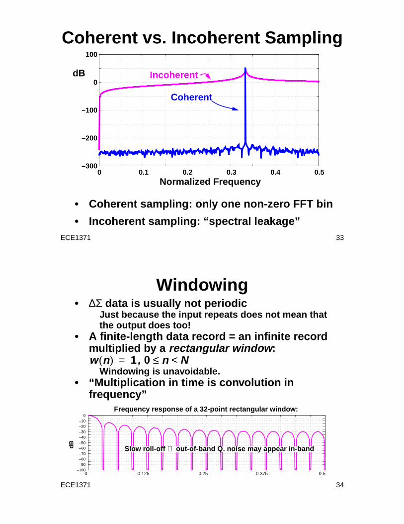
Coherent vs. Incoherent Sampling
• Coherent sampling: only one non-zero FFT bin
• Incoherent sampling: “spectral leakage”
0 0.1 0.2 0.3 0.4 0.5–300
–200
–100
0
100
dB
Normalized Frequency
Incoherent
Coherent
ECE1371 34
Windowing• ∆Σ data is usually not periodic
Just because the input repeats does not mean thatthe output does too!
• A finite-length data record = an infinite recordmultiplied by a rectangular window :
,Windowing is unavoidable.
• “Multiplication in time is convolution infrequency”
w n( ) 1= 0 n≤ N<
0 0.125 0.25 0.375 0.5–100–90–80–70–60–50–40–30–20–10
0Frequency response of a 32-point rectangular window:
Slow roll-off ⇒ out-of-band Q. noise may appear in-banddB

ECE1371 35
Example Spectral DisasterRectangular window, N = 256
0 0.25 0.5–60
–40
–20
0
20
40
Normalized Frequency, f
dB
Actual ∆Σ spectrum
Windowed spectrum
Out-of-band quantization noiseobscures the notch!
W f( ) w 2⁄
ECE1371 36
Window Comparison ( N = 16)
0 0.125 0.25 0.375 0.5–100
–90
–80
–70
–60
–50
–40
–30
–20
–10
0
Normalized Frequency, f
(dB
)
Rectangular
Hann2
Hann
Wf()
W0(
)----
--------
----

ECE1371 37
Window PropertiesWindow Rectangular Hann†
†. MATLAB’s “hann” function causes spectral leakage of tones locatedin FFT bins unless you add the optional argument “periodic.”
Hann2
,
( otherwise)1
Number of non-zeroFFT bins
1 3 5
N 3N/8 35N/128
N N/2 3N/8
1/N 1.5/N 35/18N
w n( )n 0 1 … N 1–, , ,=
w n( ) 0=
12πnN
-----------cos–
2--------------------------------
12πnN
-----------cos–
2--------------------------------
2
w 22 w n( )2∑=
W 0( ) w n( )∑=
NBWw 2
2
W 0( )2----------------=
ECE1371 38
Window Length, N• Need to have enough in-band noise bins to
1 Make the number of signal bins a small fractionof the total number of in-band bins
<20% signal bins ⇒ >15 in-band bins ⇒
2 Make the SNR repeatable yields std. dev. ~1.4 dB. yields std. dev. ~1.0 dB.
yields std. dev. ~0.5 dB.
• is recommended
N 30 OSR⋅>
N 30 OSR⋅=N 64 OSR⋅=N 256 OSR⋅=
N 64 OSR⋅=
ECE1371 39
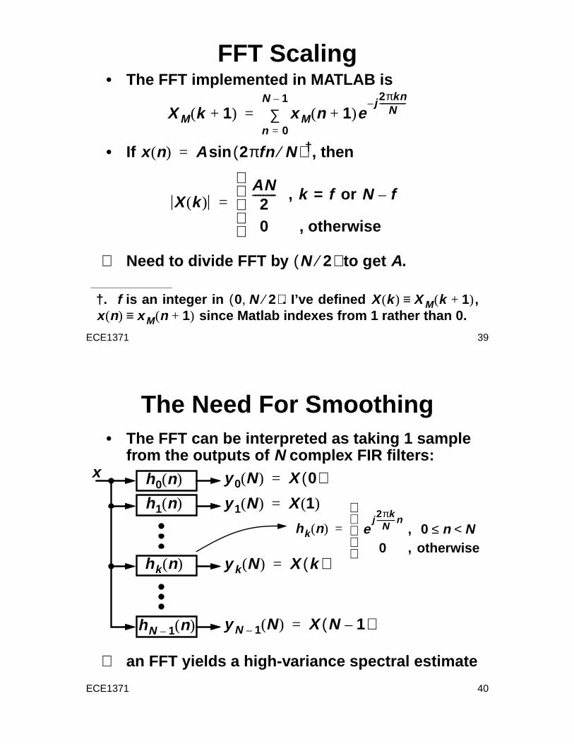
FFT Scaling• The FFT implemented in MATLAB is
• If †, then
⇒ Need to divide FFT by to get A.
†. f is an integer in . I’ve defined , since Matlab indexes from 1 rather than 0.
X M k 1+( ) x M n 1+( )ej–2πkn
N--------------
n 0=
N 1–
∑=
x n( ) A 2πfn N⁄( )sin=
0 N 2⁄,( ) X k( ) X M k 1+( )≡x n( ) x M n 1+( )≡
X k( )AN2
--------- , k = f or N f–
0 , otherwise
=
N 2⁄( )
ECE1371 40
The Need For Smoothing• The FFT can be interpreted as taking 1 sample
from the outputs of N complex FIR filters:
⇒ an FFT yields a high-variance spectral estimate
x h0 n( )
h1 n( )
hk n( )
hN 1– n( )
y 0 N( ) X 0( )=
y 1 N( ) X 1( )=
y k N( ) X k( )=
y N 1– N( ) X N 1–( )=
hk n( ) ej 2πk
N-----------n
, 0 n N<≤0 , otherwise
=
ECE1371 41
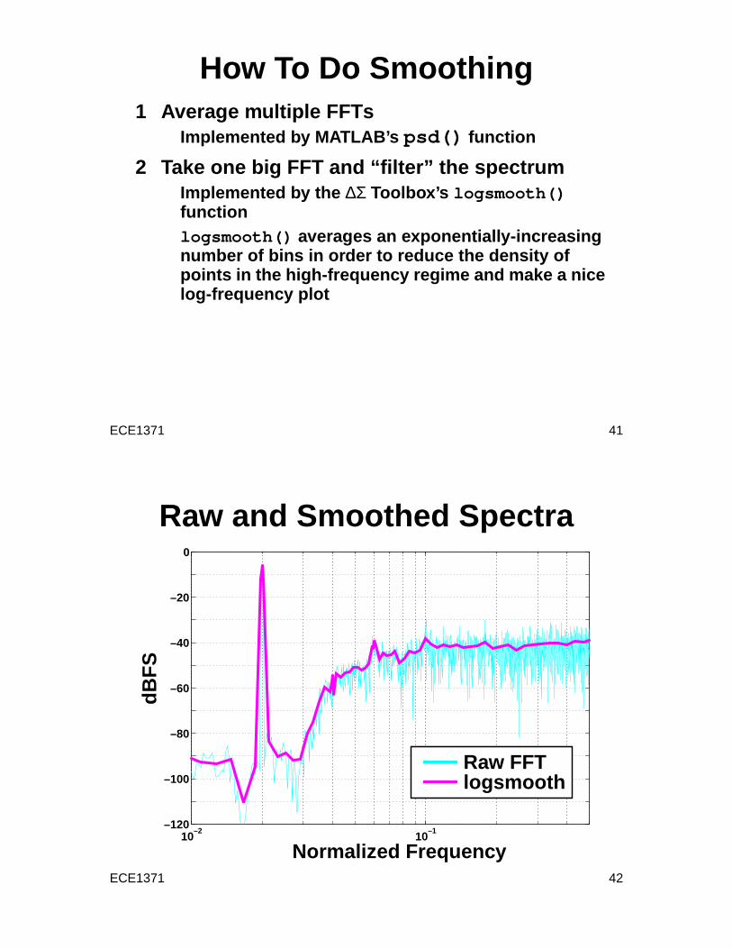
How To Do Smoothing1 Average multiple FFTs
Implemented by MATLAB’s psd() function
2 Take one big FFT and “filter” the spectrumImplemented by the ∆Σ Toolbox’s logsmooth()functionlogsmooth() averages an exponentially-increasingnumber of bins in order to reduce the density ofpoints in the high-frequency regime and make a nicelog-frequency plot
ECE1371 42
Raw and Smoothed Spectra
dBF
S
Normalized Frequency10
–210
–1–120
–100
–80
–60
–40
–20
0
Raw FFTlogsmooth
ECE1371 43
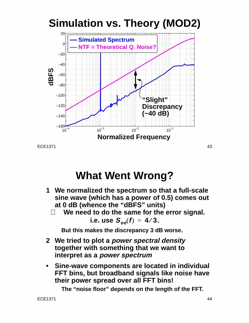
Simulation vs. Theory (MOD2)
10–4
10–3
10–2
10–1
–160
–140
–120
–100
–80
–60
–40
–20
0
20
Normalized Frequency
Simulated SpectrumNTF = Theoretical Q. Noise?
dBF
S
“Slight”Discrepancy(~40 dB)
ECE1371 44
What Went Wrong?1 We normalized the spectrum so that a full-scale
sine wave (which has a power of 0.5) comes outat 0 dB (whence the “dBFS” units)
⇒ We need to do the same for the error signal.i.e. use .
But this makes the discrepancy 3 dB worse.
2 We tried to plot a power spectral densitytogether with something that we want tointerpret as a power spectrum
• Sine-wave components are located in individualFFT bins, but broadband signals like noise havetheir power spread over all FFT bins!
The “noise floor” depends on the length of the FFT.
See f( ) 4 3⁄=
ECE1371 45
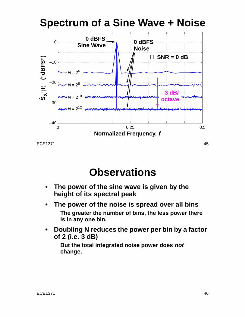
Spectrum of a Sine Wave + Noise
Normalized Frequency, f
(“dB
FS
”)S
x′f(
)
0 0.25 0.5–40
–30
–20
–10
0
N = 26
N = 28
N = 210
N = 212
0 dBFS 0 dBFSSine Wave Noise
–3 dB/octave
⇒ SNR = 0 dB
ECE1371 46
Observations• The power of the sine wave is given by the
height of its spectral peak
• The power of the noise is spread over all binsThe greater the number of bins, the less power thereis in any one bin.
• Doubling N reduces the power per bin by a factorof 2 (i.e. 3 dB)
But the total integrated noise power does notchange.
ECE1371 47
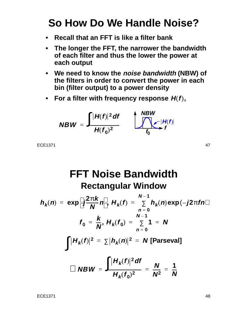
So How Do We Handle Noise?• Recall that an FFT is like a filter bank
• The longer the FFT, the narrower the bandwidthof each filter and thus the lower the power ateach output
• We need to know the noise bandwidth (NBW) ofthe filters in order to convert the power in eachbin (filter output) to a power density
• For a filter with frequency response ,H f( )
NBWH f( ) 2 fd∫H f 0( )2
----------------------------= H f( )f
NBW
f0
ECE1371 48
FFT Noise BandwidthRectangular Window
,
,
[Parseval]
∴
hk n( ) j 2πkN
-----------n exp= H k f( ) hk n( ) j– 2πfn( )exp
n 0=
N 1–
∑=
f 0kN----= H k f 0( ) 1
n 0=
N 1–
∑ N= =
H k f( ) 2∫ hk n( ) 2∑ N= =
NBWH k f( ) 2 fd∫H k f 0( )2
------------------------------- NN 2------- 1
N----= = =
ECE1371 49
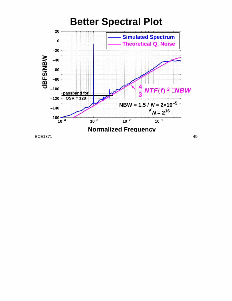
Better Spectral Plot
10–4 10–3 10–2 10–1–160
–140
–120
–100
–80
–60
–40
–20
0
20
dBF
S/N
BW
Normalized Fre quenc y
Simulated SpectrumTheoretical Q. Noise
NBW = 1.5 / N = 2×10⁻⁵
N = 216
43--- NTF f( ) 2 NBW⋅passband for
OSR = 128