Embed Size (px)
Citation preview

Signal Recovery, 2017/2018 – PD 2 Ivan Rech
Sensors, Signals and Noise 1
COURSEOUTLINE
• Introduction
• SignalsandNoise
• Filtering
• Sensors:PD2- PhotoTubes

Signal Recovery, 2017/2018 – PD 2 Ivan Rech
Vacuum Tube Photo-Diodes or Photo-Tubes 2
• PhotoTube(PT)devicestructure
• PTcurrent-voltagecharacteristicsandstationaryequivalentcircuit
• PTdynamicresponseanddynamicequivalentcircuit
• Photo-emissionofelectrons,photocathodetechnologyandPhotocathodetypes
• DetectorDarkCurrentandNoise
• PhotocathodeNoise-Equivalent-PowerNEPandDetectivity
• Low-Noisepreamplifiersforphotodiodes

Signal Recovery, 2017/2018 – PD 2 Ivan Rech
PhotoTube device structures 3
SIDE-WINDOWTUBE• Photocathode:thickopaquelayer
depositedonmetalsupportelectrode• Sidewindowoftheglasstube:
unfavourablegeometry,collection oflightonthephotocathodeisuneasyandnotveryefficient
END-WINDOWTUBE• Photocathode:thinsemitransparent layer
depositedontheinterioroftheglasstubeend
• Endwindowoftheglasstube:favourablegeometry,collection oflightonthephotocathodeiseasyandefficient
RLVAK
+-
ℎ𝜈
ℎ𝜈
A
K
-q
-q
SignaloutVA
A
RL
VAK+-
ℎ𝜈
ℎ𝜈
K
-q-q
SignaloutVA

Signal Recovery, 2017/2018 – PD 2 Ivan Rech
PhotoTube stationary I-V characteristics 4
• AtlowvoltageVAK thephotocurrentcollected attheanodeislimited bytheelectronspacechargeeffect
• AsVAK isincreasedthehigherelectric fieldreducesthespacechargeandthecurrentincreases
• AsVAK exceedsasaturationvalueVAKS allphotoelectronsarecollectedandthecurrentisconstantvs.VAK
• Thesaturation valueVAKSincreaseswiththeopticalpowerPL onthedetector
• Phototubesareoperatedbiased intothecurrentsaturationregion
IA(nA)
VAK100 200 300
200
400
IL4∝ PL4
PL =opticalpower
IL3∝ PL3
IL2∝ PL2
IL1∝ PL1
Currentsaturationregion
PTstationaryequivalentcircuit:photo-controlledcurrentgenerator
A
K
L D LI S P= ⋅

Signal Recovery, 2017/2018 – PD 2 Ivan Rech
Phototube Dynamic Response
5

Signal Recovery, 2017/2018 – PD 2 Ivan Rech
PhotoTube Dynamic Response 6
RLVAK
+-
𝑃𝐿
CL
𝐼𝐿 VA
VA
CL RLIL
PTequivalentcircuit
1L
LL L
RZsR C
=+
Maincausesthatlimitthedynamicresponse:1. Transductionfromlightfluxtodetector
current:theSER waveformhD(t) hasfinite-widthTD
2. Loadcircuit:ithasalow-passfilteraction,δ-responsehL(t) withfinite-widthTL
( ) ( ) 11 expLL L L L
th t tR C R C
⎛ ⎞= −⎜ ⎟
⎝ ⎠
Load-circuitδ-responsewith( )L LR h t⋅
Theδ-responsefromlightpower𝑃𝐿 toVA hasoverallshapehP(t) resultingfromthecascade
thewidthTP thusresultsfromquadraticaddition
andforwellexploitingthefastintrinsicresponsehD(t) ofadetector itissufficienttohave
( ) ( ) ( )P D Lh t h t h t= ∗
2 2 2 2 2P D L D L LT T T T R C= + = +
L L L DT R C T= ≤

Signal Recovery, 2017/2018 – PD 2 Ivan Rech
Fast Response AND Wide Active Area 7
Thelight-to-currenttransductionbyaphototubecanbefairlyfast,withSERpulsedurationTD around1ns.Forexploiting it,theloadfilteringmustbeadequatelylimited
• forwide-bandresponse low-valueRL isemployed;typically,RL =50Ω tomatchacoaxialcableconnection.WithTD ≈1nsandRL =50Ω, theaboverequirementimplies
• TheloadcapacitanceCL issumofCA inputcapacitanceofamplifier(orothercircuit)connected; itcanbe<1pFCS straycapacitanceofconnections; itcanbe<2pFCD electrodecapacitance;itdependsontheareaAD ofthephotocathode
• CD issmallevenforwidesensitiveareaAD ,becausethedielectric isvacuumandtheelectrodespacingiswide.Inplanegeometrywithcathode-to-anodespacingwa
e.g.withwa ≈1cm itis 𝐶( 𝑝𝐹 ≈ 0,09𝐴( 𝑐𝑚2 .It’sonly9pF forAD=100cm2
• Inconclusion: adefiniteadvantageofVacuumPhototubesisthattheyofferverywidesensitiveareatogetherwithfastresponse.Wewillseethatwithsemiconductorphotodiodesthisisnotachievable
L L DR C T≤
20LC pF≤
DD o
a
ACw
ε= ( 8,86 )o pF mε =

Signal Recovery, 2017/2018 – PD 2 Ivan Rech
Electron Photoemission and Photocathode Technology
8

Signal Recovery, 2017/2018 – PD 2 Ivan Rech
Photo-emission of electrons 9
Itisathree-stepprocess:• freeelectrongenerationbyphotonabsorption• electrondiffusioninthephotocathode layer• escapeofelectronintothevacuumSuitablematerialsaresemiconductors.Metalsareunsuitable becauseofthehighreflectivity,smalldiffusionlengthandlowescapeprobability(highpotentialstepfrominsideuptothevacuumlevel).
VacuumpotentiallevelEa ElectronAffinity
Valenceband
Conductionband
EnergyGap
VACUUM
E0
SEMICONDUCTOR
ThermalizedElectronDiffusionLengthLet ≈1– 10μm(DirectGap)
High-EnergyElectronDiffusionLengthLeh≈0,01μm(DirectGap)
Electroncollisionswithphonons≈50meVenergyloss
Signal Recovery, 2017/2018 – PD 2 Ivan Rech
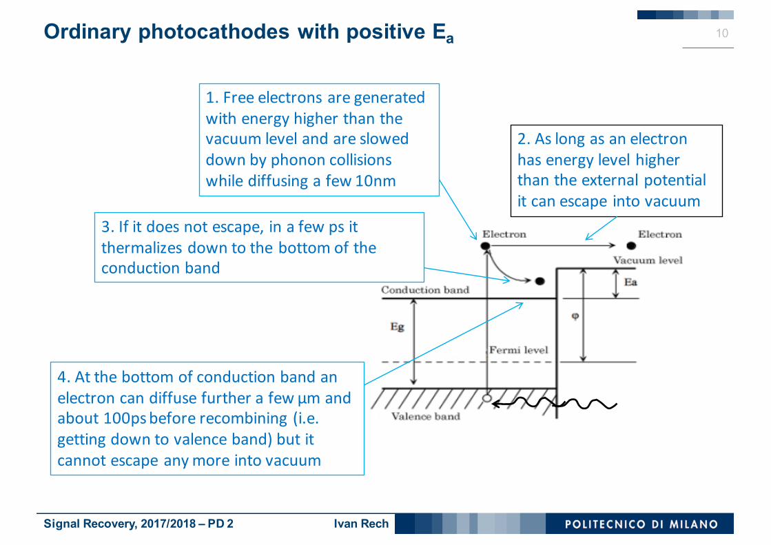
Ordinary photocathodes with positive Ea 10
1.Freeelectronsaregeneratedwithenergyhigherthanthevacuumlevelandaresloweddownbyphononcollisionswhilediffusingafew10nm
4.Atthebottomofconductionbandanelectroncandiffusefurtherafewμmandabout100psbeforerecombining(i.e.gettingdowntovalenceband)butitcannotescapeanymoreintovacuum
2.Aslongasanelectron hasenergylevelhigherthantheexternalpotentialitcanescape intovacuum
3.Ifitdoesnotescape,inafewpsitthermalizesdowntothebottomoftheconductionband

Signal Recovery, 2017/2018 – PD 2 Ivan Rech
Ordinary photocathodes with positive Ea 11
Inordertooffergoodquantumdetectionefficiency,thephotocathodematerialmustfulfillsomebasicrequirements.• Theinside-to-vacuumenergybarrierEg +Ea mustbe smallerthanthephoton
energyEp .Inthevisiblerange1,6eV<Ep<3,1eV andEg ≈1eV forsemiconductors;therefore,theelectronaffinitymustbelimited
• Electronsgeneratedindeep layersarenotemitted;escapeprobabilityishighonlyforelectronsgeneratedinasurfacelayerthatisverythin,aboutadiffusionlengthLeh ofhigh-energyelectrons.Forasignificantabsorptioninthis layertheopticalpenetration lengthLa mustanywaybeNOTmuchhigherthanLeh ;forahighabsorptionitshouldbecomparable
Inconclusion,thethicknessofthephotocathodelayercontributingtotheelectronemission isintrinsically limitedtoaboutLeh inanycase.Thatis,theactivelayerisverythin, independent fromthetotalthicknessofthephotocathode.
1aE eV≤
a ehL L≈

Signal Recovery, 2017/2018 – PD 2 Ivan Rech
Semitransparent PhotoCathodes 12
Theactivelayerofthephotocathodeisalwaysverythin,alsoforthickcathodesdepositedonametalelectrode.Thisremarkledtodevelopthinphotocathodes(withthicknessabout≈Leh )depositedontheinterioroftheglasstubeintheend-windowofthedetector.Theyarecalledsemitransparentcathodes.Theyareilluminated ontheoutersidethroughtheglasswindowendemitphotoelectronsfromtheinnerside.Theymakepossibleandeasyamuchbetteropticalcollection thantheside-windowgeometry
hν
hν

Signal Recovery, 2017/2018 – PD 2 Ivan Rech
Semi-transparent photocathode 13

Signal Recovery, 2017/2018 – PD 2 Ivan Rech
PhotoCathode Types 14
• S1 wasintroducedinthe’30sandisstill inuse.TheQEislow(peakηD≈0,4%at=800nm)butcoversawidespectrumintheIR.ItisamatrixofCesiumoxidethatincludessilvermicroparticlesandit’scurrentlydenotedAg-O-Cs.
Highlyefficientphotocathodesforthevisiblerangewereintroducedinthe’50sandprogressivelydevelopedemployingcompoundsofalkalimetals (Na,K,Cs,whichhavelowworkfunctions)andAntimony(Sb).Maintypes:• S11 rangesfrom300nmto600nm,peakηD≈15%at450nm;alkalihalideCs3Sb• S20 rangesfrom300nmto800nm,peakηD≈20%at350nm;multi-alkalihalideNa-
K-Sb-Cs• S25 extendstherangeupto800nm,peakηD≈5%at600nm;multi-alkaliNa-K-Sb-Cs
likeS20,butwithathicker layerthatgiveshighersensitivity inthered,atthecostoflowersensitivity intheblue-green
Classifications ofPhotocathodetypesaremadebyindustrialstandardcommittees.MostwidelyusedisthatbyJEDEC(JointElectronDevicesEngineeringCouncilUS),which denotescathodetypesS1,S2,...andclassifies thembyspectralresponsivitytype(ratherthanbychemicalcompositionorfabricationrecipe).

Signal Recovery, 2017/2018 – PD 2 Ivan Rech
Radiant Sensitivity or Spectral Responsivity 15
(Logscale)
(Logscale)
PHOTOCATHODETYPES
• S1(Ag-O-Csoldesttypeinfrared-sensitive)
• S11(Cs3Sbalkalihalide)
• S20Na-K-Sb-CsMulti-alkalihalide
• S25Multialkalihalideextendedredsensitivity
NB:theauxiliarylinesmarkedwithQuantumDetectionEfficiency(QE)in%makepossibletoreaddirectlyfromthediagramalsotheQE

Signal Recovery, 2017/2018 – PD 2 Ivan Rech
PhotoCathodes with negative Ea 16
Progressinsemiconductorphysicsandtechnologyledinthe’70stodeviseanewclassofphotocathodes,calledphotocathodeswithNegativeElectronAffinity(NEA)• OnaGaAscrystalsubstrate,afewatomic
layersofCesiumOxide(Cs-O)aredepositedandactivated,thusformingaverythinpositivechargelayerofCs+ ions.
• Theelectric fieldgeneratedatthesurfacecurvesdownwardtheenergybands:thevacuumpotential levelisnowlowerthanthebottomofconductionband,i.e.theelectronaffinityEa isnegative
• Electronscannowescape intovacuumalsowhenthermalizedatthebottomofconductionband;QEisthusenhanced
• Photoelectronemission isobtainedalsowithphotonswithlowerenergyEp ,downtotheGaAsenergygapEg
Inconclusion:NEAcathodesofferhigherQEvalueandbroaderspectralrange,extendinguptotheabsorptionedgeofGaAs(i.e.λ≈900nm correspondingtothegapEg ≈1,4eV)

Signal Recovery, 2017/2018 – PD 2 Ivan Rech
Detector Dark Current and Noise
17

Signal Recovery, 2017/2018 – PD 2 Ivan Rech
Detector Dark Current 18
• Afinitecurrentisemittedbyanyphotocathodeevenwhenkeptinthedark,withoutanylightfallingonit.
• Itisaspontaneousemissionduetothermaleffects(phonon-electroninteractions inthecathode)andiscalledDarkCurrent.
• ThedarkcurrentdensityjB (perunitareaofcathode)dependsonthecathodetypeandonthecathodetemperature.TypicalvaluesatroomtemperaturearereportedintheTable
PhotoCathodetype
DarkCurrent densityjB inA/cm2
DarkElectronRatedensitynB inelectrons/s·cm2
S1 ≈10-13 ≈106
S11 10-16 - 10-15 103 - 104
S20andS25 10-19 - 10-16 1 - 103
GaAsNEA 10-18 - 10-16 10 - 103

Signal Recovery, 2017/2018 – PD 2 Ivan Rech
Detector Internal Noise 19
ThetotalDarkCurrentis𝐼3 = 𝑗3𝐴( whereAD istheareaofthephotocathode.TheshotnoiseofIB isthephotodetectorunavoidableinternalnoise,witheffectivepowerdensity(unilateral)
Typicalvaluesof 𝑆3 arereportedintheTable
PhotoCathodetype
DarkCurrent densityjBA/cm2
ShotNoiseEffectivedensity 𝑆3𝑝𝐴 𝐻𝑧 𝑐𝑚2⁄
S1 ≈10-13 ≈10- 4
S11 10-16 - 10-15 ≈ 10 -5
S20andS25 10-19 - 10-16 ≈10 - 7 – 10 - 6
GaAsNEA 10-18 - 10-16 ≈ 10 – 6
2 2B B B DS qI q j A= =

Signal Recovery, 2017/2018 – PD 2 Ivan Rech
Role of the Detector Internal Noise 20
CLSi
Sv
SB
• Weknowthatforoperatingwithlow-noiseahighimpedancesensormustbeconnectedtoapreamplifierwithhighinput impedanceandlowinputnoise.Thebestavailablepreamplifiershavecurrentnoiseatroomtemperature
• Thecircuitnoise 𝑆: isalwaysdominantandthedetectorinternalnoise 𝑆3 playsinpracticenorole withanyphototube,evenfordetectorswithS1photocathodes(thathavethehighestnoise)andevenwithverywidesensitivearea(uptomanysquarecentimeters). Infact,forproducingshotnoisewithpowerdensityhigherthanthatofthecircuitnoise,thephototubedarkcurrentshouldbeIB>300pA,correspondingtoanemissionratenB >109 electrons/s.
• Vacuumtubephotodiodescanthusbeemployedforoperatingatlownoisewithoutstringentlimits tothesensitive area.Aswewillsee,thisisadefiniteadvantageoversemiconductorphotodiodes.
0,01iS pA Hz≈

Signal Recovery, 2017/2018 – PD 2 Ivan Rech
Low-noise preamplifiers for photodiodes
21

Signal Recovery, 2017/2018 – PD 2 Ivan Rech
Voltage Buffer Preamplifier 22
• Photodiodesarehigh-impedancesensors(boththevacuumphototubesandthesemiconductorphotodiodes),henceforlow-noiseoperationtheymustbeconnectedtopreamplifierswithhighinputresistance* RiA à∞ (seeslidesinOPF2)
• Simpleconfiguration:voltagebufferbasedonahigh-input-impedance andlow-noiseamplifier
*RiA =truephysicalresistancebetweentheinputterminals,notthedynamicinputresistanceincludingfeedbackeffects
Sv
iAR →∞
+
CLSiT
LR →∞ Outputvb signalSb noise
IS ≈Qδ(t)
• CL totalloadcapacitance=CD (detectorcap.) +CiA (amplifiercap.)+CS (connectioncap.)• RL totalloadresistanceà∞• Sv amplifiervoltagenoise• SiT totalcurrentnoise=SiD detectornoise+SiA amplifiernoise(+SiR loadresistornoise)
L
QC

Signal Recovery, 2017/2018 – PD 2 Ivan Rech
Voltage Buffer Preamplifier 23
Buffervoltageoutput:
Stepsignal
NoiseSpectrum
Thebufferconfigurationhassomenoteworthydrawbacks.• ThesignalamplitudeQ/CLisruledbythetotalcapacitanceCL =CD +CiA +Cs ,whose
valueisnotverysmallandnotwellcontrollable,particularlyincaseswherelongsensor-preamplifier connectionscontributearemarkableCs .CLmaybedifferentfromsampletosampleoftheamplifier,evenofthesameamplifiermodel.
• Withsignals inhigh-ratesequence,thesuperposition ofvoltagestepsmaybuild-upandproduceasignificantdecreaseofthephotodiodebiasvoltage.Thismaychangetheoperatingconditionsandconsequentlytheparametersandperformanceofthedetector,particularlyifthephotodiode isbiasednotmuchabovethesaturationvoltage.
( ) ( )1bL
Qv t tC
= ⋅
2 2
1b v iT
L
S S SCω
= +

Signal Recovery, 2017/2018 – PD 2 Ivan Rech
Alternativeconfiguration:operationalintegratorbasedonalow-noiseamplifierwithhighinput impedance
Charge Preamplifier or Transimpedance Preamplifier 24
Sv
iAR →∞+CL SiT
LR →∞
Outputvc signalSc noise
IS ≈Qδ(t) F D
Q QC C
?
FR →∞
CF
• CL totalloadcapacitance=CD (detectorcap.) +CiA (amplifiercap.)+CS (connectioncap.)• RL totalloadresistanceà∞• Sv amplifiervoltagenoise• SiT totalcurrentnoise=SiD detectornoise+SiA amplifiernoise(+SiR loadresistornoise)
• CF capacitorinfeedback.TheCF valuecanbeverysmallandisaccuratelysetbythecapacitorcomponent,becausetheinherentstraycapacitancebetweenoutputandinputpinsoftheamplifierisnegligible.Therefore,onecanworkwithCF <<CL
• RF feedbackresistorà∞
ZL
ZF

Signal Recovery, 2017/2018 – PD 2 Ivan Rech
Charge Preamplifier or Transimpedance Preamplifier 25
OutputSignal:
infrequencydomainintime
Withrespecttothebuffer,theamplitude isgreaterbythegainfactorGc =CL/CF>>1
Advantages:• Thehighersignalmakeslessrelevantthenoiseofthefollowingcircuits• Thesignalamplitude isruledbythewellcontrolledandstableCF ,nomorebythe
othercapacitancesCD ,CiA andCs• Thedetectorterminal isconnectedtotheamplifiervirtualground,hence itstays
atconstantbiasvoltageevenwithsignals inhigh-ratesequenceThenoiseanalysis(seenextslide)confirmsthattheseadvantagesareobtainedwithoutdegradingtheS/N.Thechargeamplifierconfigurationthus isthesolutionofchoiceinmostcasesmetinpractice.
L Lc b c b
F F L F
C CQ Qv v G vC C C C
= = ⋅ = ⋅ = ⋅
( ) ( )1cF
Qv t tC
= − ⋅c FF
QV QZj Cω
= − = −

Signal Recovery, 2017/2018 – PD 2 Ivan Rech
Charge Preamplifier or Transimpedance Preamplifier 26
OutputNoiseSpectrum:• thecurrentnoiseSiT isprocessedbythesametransferfunctionasthecurrentsignal• thevoltagenoiseSv isprocessedwiththetransferfunctionfromnon-invertinginput
toamplifieroutput.DenotingbyZL theloadimpedanceandbyZF thefeedbackimpedance
inourcaseZL ≈1/jωCL andZF ≈1/jωCF sothat
ifCF/CL <<1 ,withgoodapproximationitis
Withrespecttothebuffer,thesignalandnoisethusbenefitofthesamegainGc :therefore,theattainableS/Nisthesamewiththechargepreamplifieraswiththevoltagebufferpreamplifier
2 2 2
2 2 2 2
1 11 1L L Fc v iT v iT
F F F L L
C C CS S S S SC C C C Cω ω
⎡ ⎤⎛ ⎞ ⎛ ⎞⎢ ⎥= + + = + +⎜ ⎟ ⎜ ⎟⎢ ⎥⎝ ⎠ ⎝ ⎠⎣ ⎦
2 22
2 2
1L Lc v iT b c b
F L F
C CS S S S G SC C Cω⎛ ⎞ ⎡ ⎤ ⎛ ⎞
≈ + = =⎜ ⎟ ⎜ ⎟⎢ ⎥⎝ ⎠ ⎣ ⎦ ⎝ ⎠
221 F
c v iT FL
ZS S S ZZ
= + +

Signal Recovery, 2017/2018 – PD 2 Ivan Rech
NEP and Detectivity
27

Signal Recovery, 2017/2018 – PD 2 Ivan Rech
NEP and Detectivity 28
• EvaluationsandcomparisonsofPhotocathodesarecurrentlybasedontheNoiseEquivalentPowerNEP,afigureofmeritthattakesintoaccountthephotondetectionefficiencyandthedetectordark-currentnoise,butnotthepreamplifiernoise.
• NEPisdefinedwithreferencetoasituationwherethelimittotheminimummeasurablesignalissetbytheinternalnoiseofthedetector andnotbytheelectroniccircuitnoise.Wehaveseenthatthisis NOTthecasewithPhotoTubes butwewillseethatitisthecasewithPhotoMultiplierTubes.NEPwasdevisedasanfigureofmeritforcomparingobjectivelytheintrinsicqualityofdifferentdetectors.LetaphotocathodehaveareaAD ,signalcurrentIp andDarkCurrentIBwithareadensity jB .Employingafilterwithbandwidth(unilateral)Δfwehavenoise
and
Theminimummeasurablecurrentsignal Ip,min (correspondingtoS/N=1)is
ForilluminationwithopticalpowerPp atagivenλ theDetectorResponsivity is
2 2 2n B B Di qI f qj A f= Δ = Δ2
p
n
ISN i=
2,min 2p n B DI i qj A f= = Δ
[ ]1,24
pD D D
p
I mS
P hc qλ µλ
η η= = ⋅ = ⋅

Signal Recovery, 2017/2018 – PD 2 Ivan Rech
NEP and Detectivity 29
• NEPisdefinedastheinputopticalpowerPp,min correspondingtotheminimummeasurablesignal
Inessence: NEP=detectornoisereferredtothe input(inthiscasetheopticalinput).• However,theNEPisnotafullyobjectivefigureofmeritforassessingandcomparing
thequalityofphotocathodes:infact,cathodesofequalqualityhavedifferentNEPiftheyhavedifferentarea.Furthermore,theNEPisaninversescale,thatis,thebestphotocathodeshavethelowestNEPfigures.
• AdifferentfigurenamedDetectivityD*wasthereforederivedfromtheNEPbya)consideringtheNEPvaluenormalizedtounitsensitivearea(AD =1cm2)andtounitfilteringbandwidth(Δf =1Hz)b)definingtheDetectivityD*asthereciprocalofthenormalizedNEP
thatis
2,min
,min
2p n B Dp
D D D
I i qj A fNEP P
S S SΔ
= = = =
* DA fD
NEPΔ
=[ ]* 11,242 2
DD
B B
mSDqj qj
λ µη= = ⋅