Embed Size (px)
Citation preview

INTRODUCTION OF AN OPERATIONAL AMPLIFIER

What can you do with Op amps?
• You can make music louder when they are used in stereo equipment. used in stereo equipment.
• You can amplify the heartbeat by using them in medical cardiographsin medical cardiographs.
• You can use them as comparators in heating tsystems.
• You can use them for Math operations You can use them for Math operations like summing, integration etc.

Why So MANY AMPS???Why So MANY AMPS???
Lots of Specifications pSome are Important for Different ApplicationsApplications
Each Amplifier is Designed to Improve or Optimize One or a Combination ofOptimize One or a Combination of Specifications.
3

Basic op ampBasic op‐amp
Op‐amp has two inputs ,connect to two terminals
introduction
and one output.

Operational Amplifier (OpAmp)
Input 1+Vcc
p p ( p p)
• Very high differential gainHi h i t i d
Vd
+ Vo
Input 1
Output
• High input impedance• Low output impedance• Provide voltage changes −
Rin~inf Rout~0Input 2
p
-Vcc
Provide voltage changes (amplitude and polarity)
• Used in oscillator, filter and Rin~inf Rout 0Vccinstrumentation
• Accumulate a very high gain by multiple stages
o dV AV=by multiple stages.
• .5
A : differential gain normally very large, say 10
Ref:080114HKNOperational Amplifier
5

Single‐Ended Inputg p
+ V+
−
Vo
~ Vi
• + terminal : Source• – terminal : Ground• 0o phase change
+ Vo • + terminal : Ground• – terminal : Source• 180o phase change−
~ Vi
80 p ase c a ge
Ref:080114HKN Operational Amplifier 6

Double‐Ended InputDouble Ended Input
• Differential input+ VoVd
p
−+ −= VVVd
−~
Ref:080114HKN Operational Amplifier 7

CommonMode Operationp
+Same voltage source is +
−Vo
Same voltage source is applied at both terminals.
Vi ~Ideally, two input are equally amplified
Output voltage is ideally zero due to differential voltage is zero
Note for differential circuits:Opposite inputs : highly amplified
zero
Practically, a small output signal can still be measured
Common inputs : slightly amplified
⇒ Common‐Mode Rejection
Ref:080114HKN Operational Amplifier 8
signal can still be measured

Common‐Mode Rejection Ratio (CMRR)Common Mode Rejection Ratio (CMRR)Differential voltage input :
VVV +Noninverting Input
−+ −= VVVd
Common voltage input :
+
−
Input
Inverting Output
)(21
−+ += VVVc
GGCommon‐mode rejection ratio:
Input
Output voltage :
ccddo VGVGV +=
)dB(log20CMRR 10c
d
c
d
GG
GG
==
ccddo
Gd : Differential gainGc : Common mode gain
Note:When Gd >> Gc or CMRR →∞⇒Vo = GdVd
Ref:080114HKN Operational Amplifier 9

What is an “Ideal” Op Amp?
+VIN
+
‐GX Y
VOUT
Amplifies a small signal (X) to a larger signal (Y) by Gain of G
OUT
Ideal Op Amp Characteristics :– Voltage at + Input = Voltage at Input– Infinite Input Impendence– Zero Output Impendence– Infinite Open Loop Gain
• In closed loop Negative Input=Positive Input– Infinite Bandwidth

Op Amp Equivalent CircuitOp Amp Equivalent Circuit
vd = v2 – v1A is the open‐loop voltage gainvv2
v1Voltage controlled gvoltage source

AC EQUIVALENT OF OPERATIONAL AMPLIFIERAC EQUIVALENT OF OPERATIONAL AMPLIFIER
RoV o
_
V1
+
Ri AVd
+
Vd
V2
Vo
V2 _
Figure 8.6: Working circuit diagram of op amp.
10
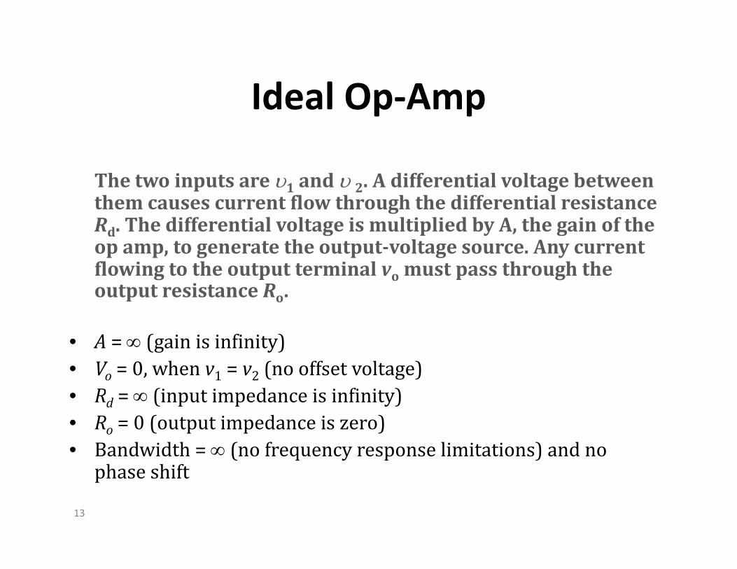
Ideal Op‐AmpIdeal Op Amp
Th t i t d A diff ti l lt b t The two inputs are υ1 and υ 2. A differential voltage between them causes current flow through the differential resistance Rd. The differential voltage is multiplied by A, the gain of the op amp to generate the outputvoltage source Any current op amp, to generate the outputvoltage source. Any current flowing to the output terminal vo must pass through the output resistance Ro.
• A = ∞ (gain is infinity)• Vo = 0, when v1 = v2 (no offset voltage)R (i t i d i i fi it )• Rd = ∞ (input impedance is infinity)
• Ro = 0 (output impedance is zero)• Bandwidth = ∞ (no frequency response limitations) and no
h h fphase shift
13

WHY IT IS CALLED AN OPAMP?WHY IT IS CALLED AN OP AMP?
Op‐Amps circuits can perform mathematicalOp Amps circuits can perform mathematical operations on input signals:– addition and subtraction– addition and subtraction
– multiplication and division
differentiation and integration– differentiation and integration
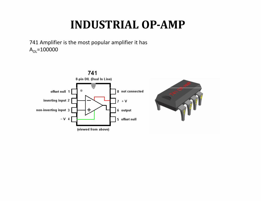
INDUSTRIAL OPAMP741 Amplifier is the most popular amplifier it hasAOL=100000

The 741 Op‐amp
The most common op‐amp is the 741 IC.

OP AMP BLOCK DIAGRAMOP‐AMP BLOCK DIAGRAM+ V
Inverting Input (- VIN)
OutputDifferential Amplifier
Voltage Amplifier
Output Amplifier
V
Noninverting Input (+ VIN)
Figure 1 Op Amp Block Diagram
- V

OP‐AMP HAS 3 –STAGE AMPLIFIER CIRCUITS
• First Stage : Differential Amplifier ‐it gives theFirst Stage : Differential Amplifier it gives the OP‐AMP high input impedance (resistance)
• Second Stage: Voltage Amplifier – it gives highSecond Stage: Voltage Amplifier it gives high gain
• Third Stage : Output Amplifier (EmitterThird Stage : Output Amplifier (Emitter Follower) – gives low output impedance (resistance)

Generic View of Opamp Internal Structure
• An op‐amp is usually comprised of at least three different amplifier stages (see figure)
– Differential amplifier input stage with gain a (v ‐ v ) having– Differential amplifier input stage with gain a1(v+ ‐ v‐) having inverting & non‐inverting inputs
– Stage 2 is a “Gain” stage with gain a2 and differential or singled ended input and output
– Output stage is an emitter follower (or source follower) stage with a gain = ~1 and single ended output with a large currentwith a gain = 1 and single‐ended output with a large current driving capability

Symbol of OP‐AMPSymbol of OP AMP
-VIN -VIN
+VS
-
+VIN
VOUT
-
+VIN
VOUT
+
+VIN
+
IN
-VS
(a) Without power connection (b) With power connection
Figure 5 Op Amp Schematic Symbols

DUAL SUPPLY OR DUAL BATTERYDUAL SUPPLY OR DUAL BATTERY
Most Op Amps require dual power supplyMost Op Amps require dual power supply with common ground
Positive Supply (+15V) to pin7Positive Supply (+15V) to pin7Negative Supply (‐15V) to pin4
+V
-VIN
-
VOUT
+VS
7
++VIN
OUT
-VS
4
Common Ground
Figure 6 Dual Supply Voltages connection
S

Some Op Amps work on single supply alsoSome Op Amps work on single supply also
-VIN
-V7
-VIN
-V
+VS
7
++VIN
VOUT7
4+
+VIN
VOUT7
4
-VS
(a) Single Positive Voltage (b) Single Negative Voltage
Figure 7 Single Supply Voltages connection

ADVANTAGE OF DUAL POWER SUPPLYADVANTAGE OF DUAL POWER SUPPLY
Using dual power supply will let the op ampUsing dual power supply will let the op amp to output true AC voltage.
+15V +30V
0V
-15V
Output
0V
Output 30 V30 V
Figure 8a Op Amp powered from Dual supply Figure 8b Op Amp powered from Single supply

What is dual power supply?What is dual power supply?
Single Power Supply Single Power Supply
Figure 18 Dual Power Supply
Common +15V–15V
Figure 18 Dual Power Supply

PIN/OR BASED DIAGRAM OF AN OP‐AMPPIN/OR BASED DIAGRAM OF AN OP AMP
1 8+VCC
7411 8
+VCC
2
3 6
7-
+
2
3 6
7-
+
4 5-VEE
4 5-VEE
Figure 3 Op Amp pins Identification
b) Notched Packagea) Dot marked Package

What are these pins?What are these pins?
1 81. Offset
Null 8. N / C741
2
3 6
7
6 Output
7. +VCC
3. Noninverting Input
2. Inverting Input –VIN
3
4 5
6
-VEE
6.Output+VIN
5.Offset Null
Figure 4 Op Amp pins Description

What are these pins?What are these pins?
• Pin 1 and Pin 5 : Offset null input, are used to remove the Off lOffset voltage.
• Pin 2: Inverting input (‐VIN), signals at this pin will be inverted at output Pin 6.
• Pin 3: Non‐inverting input (+VIN), signals at pin 3 will be processed without inversion.
• Pin 4: Negative power supply terminal (‐VEE). • Pin 6: Output (VOUT) of the Op‐Amp• Pin 7: Positive power supply terminal (+VCC)• Pin 8: No connection (N\C) it is just there to make it aPin 8: No connection (N\C), it is just there to make it a standard 8‐pin

OPAMP CHARACTERSTICS
High voltage gain ,in the value 10000‐100000
High input impedance, 1 to 2 mega ohm.
Small output impedance, around 100 ohm.p p
Infinite bandwidth
L CMRR d i d ib lLarge CMRR , expressed in decibels.
range : 70‐80dbs
Large slew rate normally around 0.5v/microsec
Ref:080114HKN Operational Amplifier 28

OP‐AMP CONFIGURATIONSOP AMP CONFIGURATIONS
Figure Types of Feedback
(a) No Feedback (open loop
comparator circuit)
(b) Negative Feedback
(c) Positive Feedback

FEEDBACKFEEDBACK
• No feedback : Open loop (used inNo feedback : Open loop (used in comparators)
• Negative feedback : Feedback to the inverting• Negative feedback : Feedback to the inverting input (Used in amplifiers)
P i i f db k F db k h• Positive feedback : Feedback to the non inverting input (Used in oscillators)

OPERATIONAL AMPLIFIER IN OPEN LOOPOPERATIONAL AMPLIFIER IN OPEN LOOP
As an amplifier, an op‐amp in open loop is l d d It drarely used or never used. It can used as a
comparator.

SaturationSaturation
• VOUT cannot exceed the supply voltages.• In fact, typically VOUT can only get to within
b 1 5 V f h liabout 1.5 V of the supplies.
VOUT VOUT
OUT OUT
t t
Desired Output Waveform Actual Output Waveform

OPEN LOOP OPAMP AS COMPARATOROPEN LOOP OP AMP AS COMPARATOR
• COMPARATOR: is the circuit whichCOMPARATOR: is the circuit which compares two voltages signal.
THE CIRCUIT DIAGRAM IS :

OP AMP as a Comparator (compares 2 voltages and produces a signal to indicate voltages and produces a signal to indicate
which is greater)
+VS
VO
+VIN > –VIN
+VS
V
+VIN = –VIN0VO
+VIN
–VIN
–VS
+VIN < –VIN
–VS
( ) C t Ci it (b) C t O t t(a) Comparator Circuit (b) Comparator Output
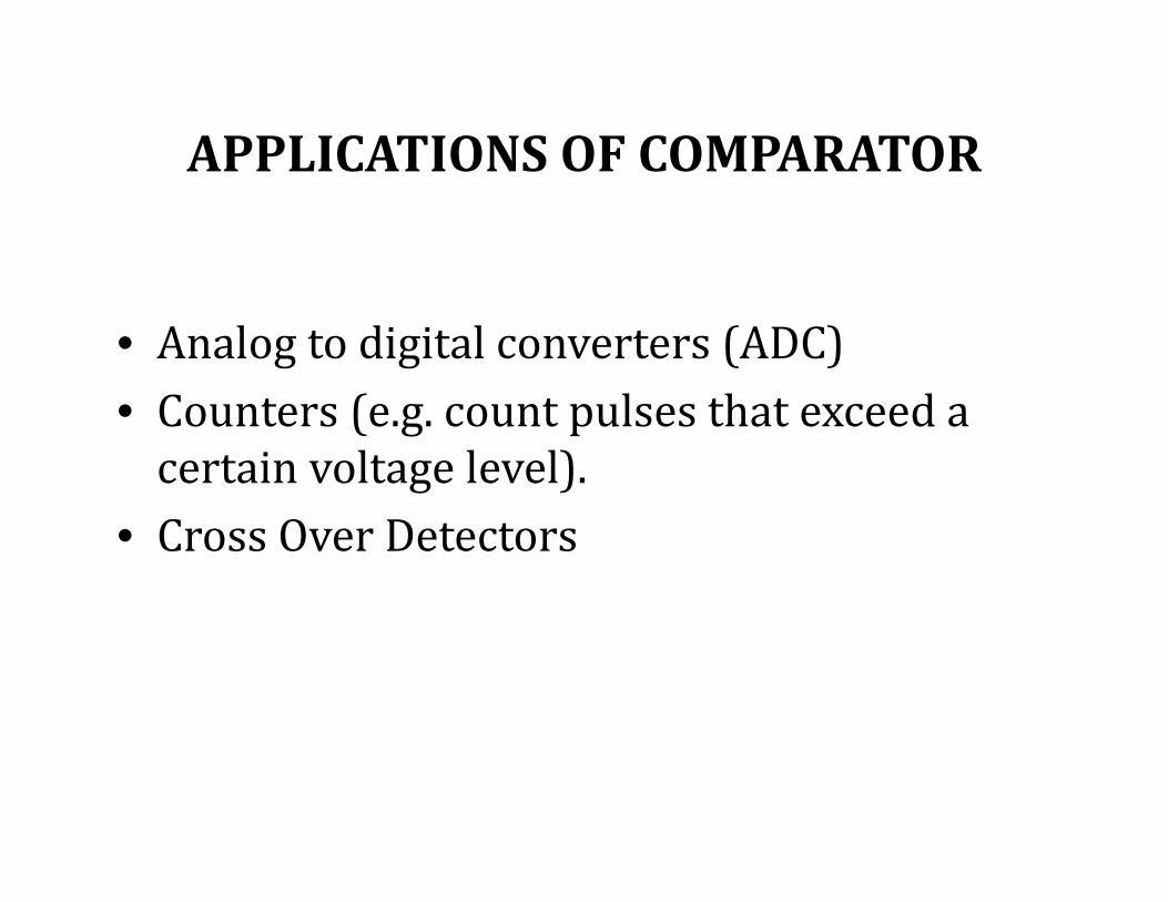
APPLICATIONS OF COMPARATORAPPLICATIONS OF COMPARATOR
• Analog to digital converters (ADC)( l h d• Counters (e.g. count pulses that exceed a
certain voltage level).• Cross Over Detectors

APPLICATION OF OPAMP AS AN AMPLIFIER
There are three amplifiers.There are three amplifiers.
1) The non inverting amplifier with1) The non‐inverting amplifier with feedback.
2)The inverting amplifier with feedback.
3)The differential amplifier.

APPLICATION OF OPAMP :THE NONINVERTING AMPLIFIER
The circuit of the non‐inverting amplifierThe circuit of the non inverting amplifier with feedback is :

The voltage divider circuit is :

The output will be : ( )o A Bv A v v= −
In the fig And will be voltage across
( )o A B
v v= vIn the fig. And will be voltage across resistance ,i.e feedback voltage
in Av v= Bv
gR fv
By the help of voltage divider circuit: the current is :
o u t
f g
viR R
⎛ ⎞= ⎜ ⎟⎜ ⎟+⎝ ⎠
And the feedback voltage is : gB f out
Rv v v
R R⎛ ⎞
= =⎜ ⎟⎜ ⎟+⎝ ⎠f gR R⎜ ⎟+⎝ ⎠

Now substitute the values of and Av Bvin the output equation :
A B
( )o A Bv A v v= −
So the exact expression for the voltage gain is :( )A R R+( )f gout
in f g g
A R Rvv R R AR
+=
+ +
Here,
Theng f gAR R R+f
AR AR+ fRvThen g fout
in g
AR ARvv AR
+= 1 fout
FBin g
vAv R
= = +

N i ti lifi i l tNon‐inverting amplifier is very close to an ideal voltage amplifier. And this can be shown b i th t f f db kby using the concept of feedback.
from equation : gB f out
Rv v v
R R⎛ ⎞
= = ⎜ ⎟⎜ ⎟+⎝ ⎠
as we know in the feedback network :
f gR R⎜ ⎟+⎝ ⎠
1 Aβ+as we know in the feedback network :
where is the closed loop gain
i th f t
βAβ
fv is the factor.f
o u t
vv
β =

So v R⎛ ⎞So f g
out f g
v Rv R R
β⎛ ⎞
= = ⎜ ⎟⎜ ⎟+⎝ ⎠
And then using in the ( )f gout
FBin f g g
A R RvAv R R AR
+= =
+ +
We got
f g g
1FB
g
AAR
A=
⎛ ⎞⎜ ⎟ 1FB
AAAβ
=+1 g
f g
AR R
+ ⎜ ⎟⎜ ⎟+⎝ ⎠1 Aβ+
1Aβ f
1Or
This is highly stable.
1FBA
β=
g y

Input impedance with feedback is increasesInput impedance with feedback is increases that is : ( )1if iR R Aβ= +
Output impedance is reduced with feedback :R
B d idth ill i b f i
( )1o
ofRR
Aβ=
+
Bandwidth will increase because of gain bandwidth product. ( )1f oBW f Aβ= +
non‐inverting amplifier is a ideal voltage gain.
( )f

APPLICATION OF OPAMP THE INVERTING AMPLIFIER
The circuit of the inverting amplifier withThe circuit of the inverting amplifier with feedback is :

This is a voltage shunt feedback circuitThis is a voltage shunt feedback circuit.
ANALYSIS FOR VOLTAGE GAINANALYSIS FOR VOLTAGE GAIN :
Let us see here, input current divided into two parts and so,
iifi
bi
Summing up currents at gives :2v
i b fi i i= +i b f

Input impedance of op‐amp is extremely largeInput impedance of op amp is extremely large so is very close to zero.
bi0i 0bi ≈
So ii = fi
The value of and ii fi
2ii
v viR−
= 2 0f
f
v viR−
=1R fR

Then in equation i i=Then in equation i fi i=
2 2 0iv v v v− −2 2 0
1
i
fR R=
Let this equation is denoted by ………….x
The gain of the amplifier A is ratio of outputThe gain of the amplifier A, is ratio of output voltage to the two inputs.
SoSo
1 2
ovAv v
=−1 2

But is zero becouse it is grounded.
So 0
2
vAv
⎛ ⎞= −⎜ ⎟
⎝ ⎠2⎝ ⎠
02
vvA
⎛ ⎞=−⎜ ⎟⎝ ⎠
Put the value of in equation ……x
2 A⎜ ⎟⎝ ⎠
Than the voltage gain with feedback will be :
0 fFB
ARvAR R AR
= =−1 1
FBi fv R R AR+ +
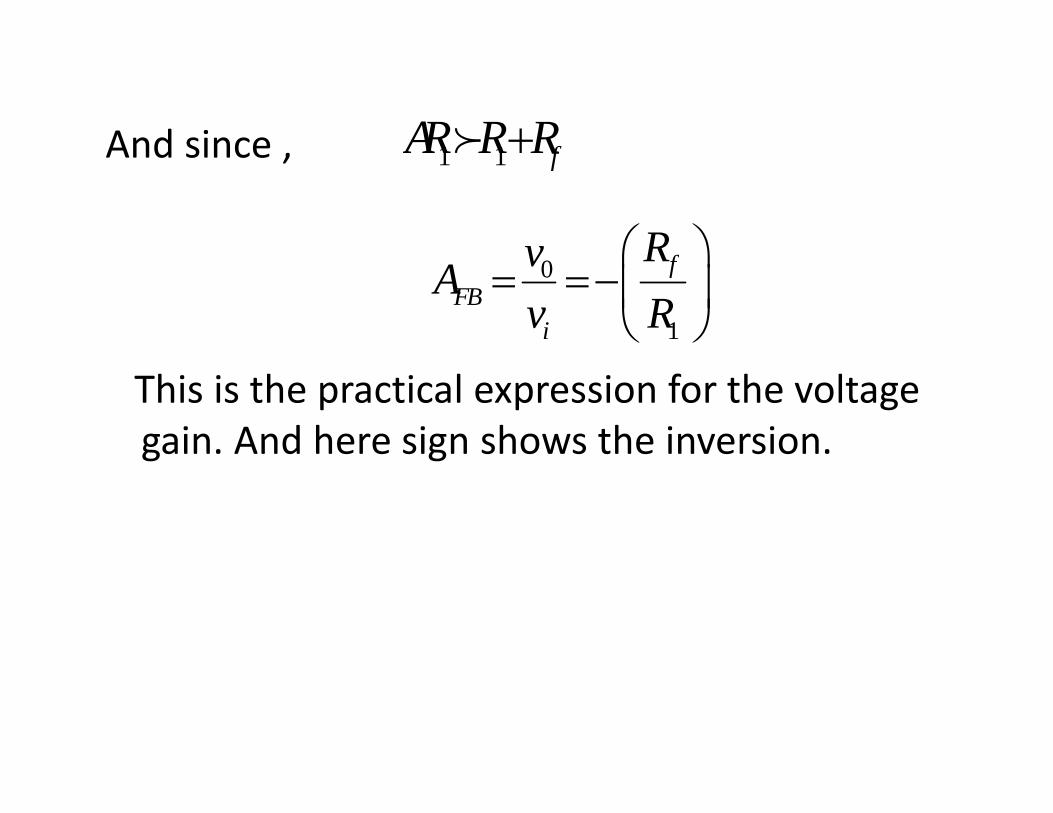
And since 1 1 fAR R R+fAnd since , 1 1 fAR R R+f
Rv ⎛ ⎞0
1
fFB
i
RvAv R
⎛ ⎞= =−⎜ ⎟
⎝ ⎠This is the practical expression for the voltage gain. And here sign shows the inversion.g g

Input Resistance for Inverting and Noninverting Op ampsinverting Opamps
The non‐inverting op‐amp configuration of slide 2‐4 has an apparent input resistance of infinity, since iIN = 0 and RIN = vIN/iIN = vIN/0 = infinity
The inverting op‐amp configuration, however, has an apparent input resistance of R1
– since RIN = vIN/iIN = vIN/[(vIN – 0)/R1] = R1since RIN vIN/iIN vIN/[(vIN 0)/R1] R1
R. W. KnepperSC412, slide 2‐7

APPLICATION OF OPAMP THE DIFFERENTIAL AMPLIFIER
The circuit diagram of the differential amplifierThe circuit diagram of the differential amplifier is :
v3
v4

Output of the differential mode : ( )Ap ( )0 1 2v A v v= −
Case 1: let be grounding so the output will be bv
1
foa a
Rv v
R⎛ ⎞
= −⎜ ⎟⎝ ⎠
Case 2: let be grounded, than current is 1⎝ ⎠
av
2 3
bviR R
=+

Then ⎛ ⎞Then 1 3
2 3
bvv RR R⎛ ⎞
=⎜ ⎟+⎝ ⎠
R⎛ ⎞And output due to will be:bv1
1
1 fob
Rv v
R⎛ ⎞
= +⎜ ⎟⎝ ⎠
Now substitute the value of 1v
This is the output.3
1 2 3
1 fob b
R Rv vR R R
⎛ ⎞⎛ ⎞= + ⎜ ⎟⎜ ⎟ +⎝ ⎠⎝ ⎠
Now let resistances R R= R R=1 2R R= 3fR R=

Th t fR⎛ ⎞Than we got :1
fob b
Rv v
R⎛ ⎞
= ⎜ ⎟⎝ ⎠
now we apply the superposition theorem and it will be :
o oa obD
a b a b
v v vAv v v v
+= =
− −a b a b
fRA
⎛ ⎞= ⎜
The output will be : 1
DAR
=−⎜⎝ ⎠
( )v A v v= −( )0 D a bv A v v=

Input impedance of differential amplifier :for p p pinverting input :
( ) 1R R≈( ) 1i aR R≈
And for non‐inverting input :
( ) 2 3 1 fibR R R R R= + = +

DIFFERENTIAL AMPLIFIERDIFFERENTIAL AMPLIFIER
Disadvantage of one‐op‐amp differential amplifier is its low input resistance.
56
OPAMP LIMITATIONS
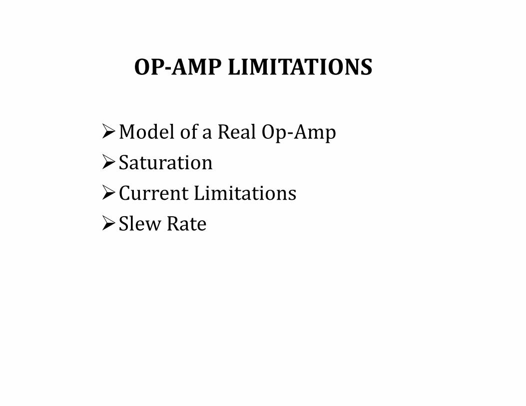
M d l f R l O AModel of a Real Op‐AmpSaturationCurrent LimitationsSlew RateSlew Rate

Ideal Vs Practical Op‐AmpIdeal Vs Practical Op AmpIdeal Practical
+ AVIdeal op-amp
Open Loop gain A ∝ 105
Bandwidth BW ∝ 10-100Hz −
~AVin
Vin Vout
Zout=0
Input Impedance Zin ∝ >1MΩ
Output Impedance Z 0 Ω 10 100 ΩOutput Impedance Zout 0 Ω 10-100 Ω
Output Voltage VoutDepends only on Vd = (V+−V−)
Depends slightly on average input V (V +V )/2
+Vi Vout
ZoutZin
Practical op-amp
Differential mode signal
Vc = (V++V−)/2 Common-Mode signal
CMRR ∝ 10-100dB
− AVin
Vin Vout~
Ref:080114HKN Operational Amplifier 58
CMRR ∝ 10 100dB

OPAMP APPLICATIONSOP AMP APPLICATIONS
Voltage followerVoltage followerCurrent to voltage converterSumming amplifierSumming amplifierSign changerS li i hti lifiScaling or weighting amplifierAveraging amplifierLogarithmic amplifierThe integrator

The low pass filterThe low pass filterThe high pass filterh b d f lThe band pass filterActive filterThe instrumentation amplifierThe comparatorThe comparatorThe difference amplifierA di lifiAudio amplifier

VOLTAGE FOLLOWER
Special case of non‐inverting amplifier is aSpecial case of non inverting amplifier is a voltage follower.Since in the non inverting amplifierSince in the non‐inverting amplifier.
where is feedback resistance.2R

=>

We have made in the basic non inverting0R =We have made in the basic non‐inverting amplifier and
2 0R =
1R = ∞
gain of non‐inverting amplifier will be –Gain = 2
1
1 RR
+
when th i d d t 1
2 0R =
than gain reduced to 1.

When gain is 1 than,
0 iv Av=
Application of voltage follower
0 iv v=
Application of voltage follower :As buffer amplifier : Used as a buffer, to prevent a high source resistance from being loaded down by a l i l d I h d ilow‐resistance load. In another word it prevents drawing current from the source.

CURRENT TO VOLTAGE CONVERTER
This is the modification of the inverting amplifier i.e modified inverting amplifier.
The basic circuit of a inverting amplifier is :The basic circuit of a inverting amplifier is :

Operation of an “Ideal” Inverting AmplifierAmplifier
VVirtual Ground Because +V = V
I21
1RVI in
=+VIN = ‐VIN
R2
Vin Vout
I1
0 RVV in
21 II =
+
‐
R1
)(
0
2
21
RVV
RR
Vout −=
)(1R
VV inout −=

, becouse it is a virtual ground then,2 0v = , g ,2 0v
2ini
v vIR−
=1R
inv I1
iniI
R=

put in equation this :ini
v IR
= v⎛ ⎞
We are getting :1R
21
ino
vv RR
⎛ ⎞= −⎜ ⎟
⎝ ⎠
2o iv I R= •
o iv Iα
that is the expected from current to voltage
o i
that is the expected from current to voltage converter.

So the modified inverting amplifier will be :g p

APPLICATION:APPLICATION:
A h dAs photo detector

APPLICATIONS FOR MATHEMATICAL OPERATIONS
SIGN CHANGER : using inverting amplifierSIGN CHANGER : using inverting amplifier.The basic circuit of inverting amplifier :

As we know the closed loop gain of theAs we know the closed loop gain of the inverting amplifier will be :
F outR vA −= =FB
in in
AR v
= =
now if we choose here the two resistances as of same magnitude so,
in this case,in FR R=
,1F BA =

1A 1FBAv v
== −
So these two will of identical magnitude out inv v=
becouse gain is 1.so sign has changed.g g
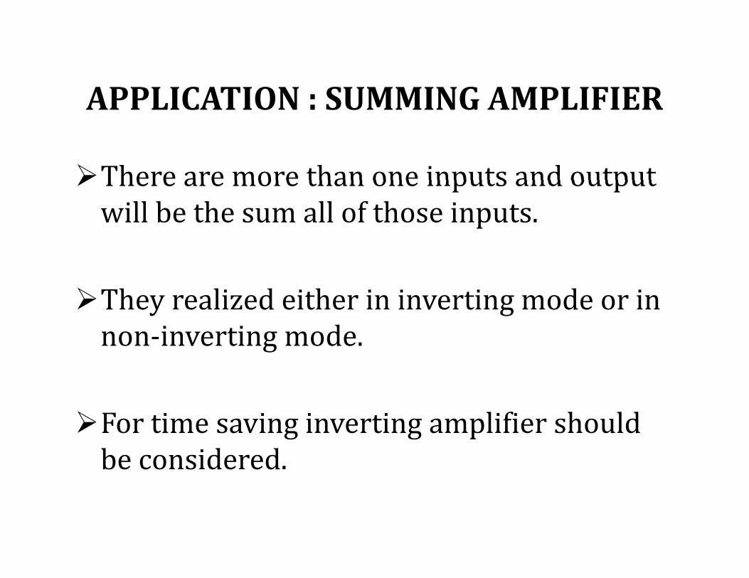
APPLICATION : SUMMING AMPLIFIERAPPLICATION : SUMMING AMPLIFIER
There are more than one inputs and outputThere are more than one inputs and output will be the sum all of those inputs.
They realized either in inverting mode or in dnon‐inverting mode.
For time saving inverting amplifier should be considered.

The basic circuit is shown below :The basic circuit is shown below :
Virtual-ground equivalent circuit.

:use KCLI I I I I+ + = +1 2 3
0;R R R b Rf
b
I I I I I
while IV V V V V V V V
+ + = +
=
1 2 3
1 2 3
: b b b b o
f
V V V V V V V VsoR R R R− − − −
+ + =
1 2 3
1 2 3
0; ob
f
V V V Vinsert VR R R R
−= + + =
1 2 3
1 2 3o f
V V VV RR R R
⎛ ⎞= − + +⎜ ⎟
⎝ ⎠1 2 3R R R⎝ ⎠

1 2 3V V VV R⎛ ⎞
+ +⎜ ⎟
This is the basic equation. From this equation we
1 2 3
1 2 3o fV R
R R R= − + +⎜ ⎟
⎝ ⎠q q
can go for the summing amplifier.
in this basic equation if choose : (say)R R R R= = =in this basic equation if choose : (say)
Than ,
1 2 3R R R R= = =
( )1 2 3f
o
Rv v v v⎛ ⎞= − + +⎜ ⎟
⎝ ⎠If further we choose than magnitude of gain = 1,
( )1 2 3o R⎜ ⎟⎝ ⎠
fR R= 1,
In that case , ( )1 2 3ov v v v= − + +( )1 2 3o

APPLICATION :SCALING OR WEIGHTED AMPLIFIER
Scaling or weighted amplifier is the one inScaling or weighted amplifier is the one in which the each input voltage is amplified differentlydifferently.

EXAMPLE :if we want that the output
should be :should be : ( )1 2 34 0.5 1.5ov v v v= + +
Where are input voltages than the 1 2 3, ,v v voutput should meet this requirement?

For that,let, 12fR = ΚΩ
Than we sholud choose So that factor will come out are :
1 3R = ΚΩ2 24R = ΚΩ 2 8R = ΚΩ
12 83=
12 0.524
=12 1.58=
They all resistance are different and then :
3 24 8
They all resistance are different and then :
This is the scaling or weighted amplifier( )1 2 34 0.5 1.5ov v v v= − + +
This is the scaling or weighted amplifier.

APPLICATION: AVERAGING AMPLIFIERAPPLICATION: AVERAGING AMPLIFIER
Here average of all the inputs put togetherHere average of all the inputs put together.Consider the same ckt and the basic equation:
the basic equation is :
V V V⎛ ⎞1 2 3
1 2 3o f
V V VV RR R R
⎛ ⎞= − + +⎜ ⎟
⎝ ⎠

if 1 2 3R R R R= = =
And where is the no of inputs
1 2 3
1fR= NAnd where is the no. of inputs . f
R N= N
1RHere is the three inputs so, 13
fRR
=
Now if we substitute in basic equation ,the output will be :output will be :
( )1 2 30 3
v v vv
+ += −0 3

Typical Op Amp ParametersTypical Op Amp Parameters
Parameter Variable Typical Ranges Ideal Values
Open‐LoopV lt G i
A 105 to 108 ∞Voltage Gain
Input Resistance
Ri 105 to 1013Ω ∞ΩResistance
Output Resistance
Ro 10 to 100Ω 0ΩResistance
Supply Voltage Vcc/V+
‐Vcc/V‐5 to 30 V‐30V to 0V
N/AN/A

Types of Closed Loop GainTypes of Closed Loop Gain
Gain Variable Equation UnitsName
q
Voltage Gain AV vo/vs None or V/V
Current Gain AI io/is None or A/A
Transresistance Gain AR vo/is V/A or Ω1Transconductance
GainAG io/vs A/V or Ω−1

Applications of Op‐AmpsApplications of Op Amps• Electrocardiogram (EKG) Amplification
N d t diff i lt f l d 1 d l d– Need to measure difference in voltage from lead 1 and lead 2
– 60 Hz interference from electrical equipment

Applications of Op‐Amps• Piezoelectric Transducer
– Used to measure force, pressure, acceleration
– Piezoelectric crystal generates an electric charge in response to deformation
• Use Charge Amplifier– Just an integrator op‐amp circuitJust an integrator op amp circuit
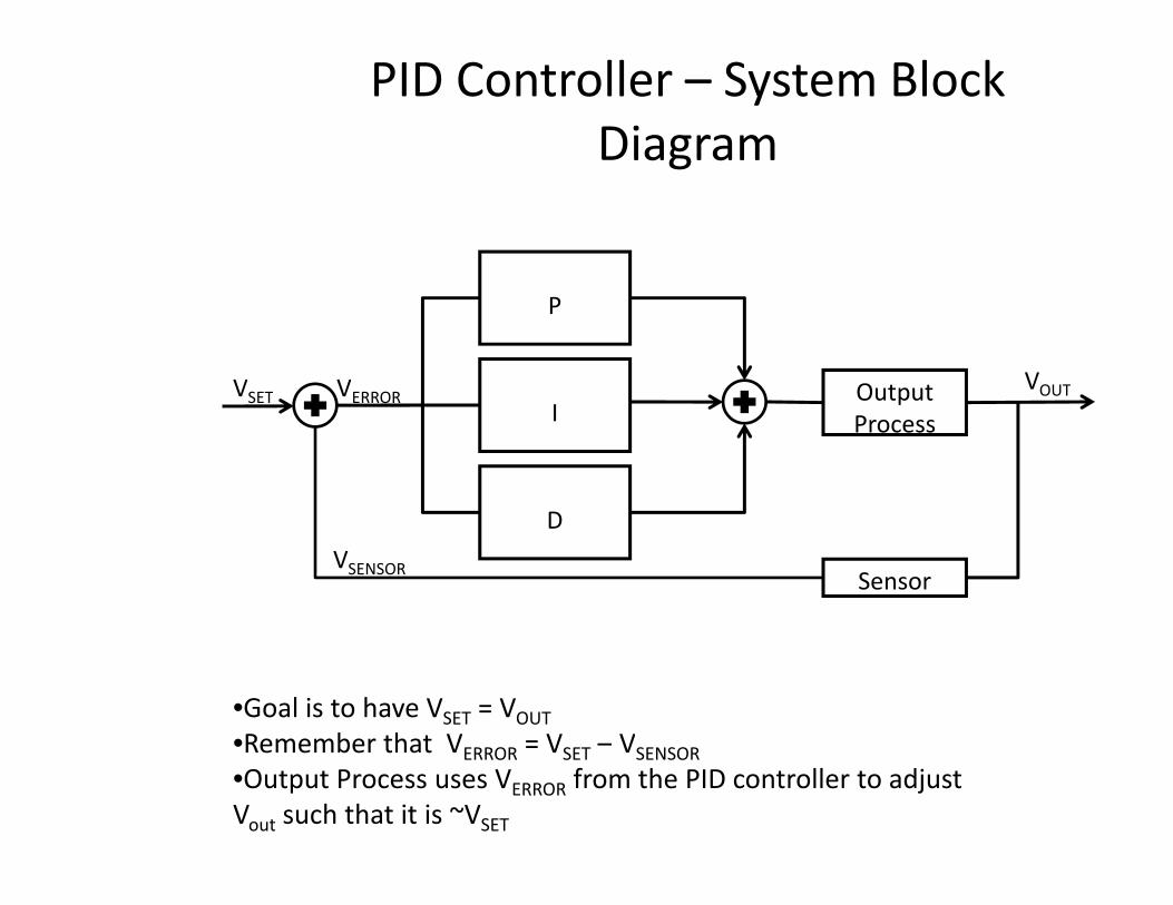
PID Controller – System Block Diagramg
P
OutputVERRORVSETVOUT
IOutput Process
VERRORVSET OUT
D
SensorVSENSOR
•Goal is to have VSET = VOUTR b th t V V V•Remember that VERROR = VSET – VSENSOR
•Output Process uses VERROR from the PID controller to adjust Vout such that it is ~VSET

ApplicationsPID Controller – System Circuit DiagramPI Controller System Circuit iagram
Signal conditioning allows you to introduce a time delay which could
account for things like inertiaaccount for things like inertia
Calculates VERROR = ‐(VSET + VSENSOR)
System to control
‐VSENSOR
Source: http://www.ecircuitcenter.com/Circuits/op_pid/op_pid.htm

ApplicationsPID Controller – PID Controller Circuit Diagram
Adjust ChangeKp RP1, RP2Ki RI, CI
VERR
Kd RD, CD
VERR PID

Basic Electric CircuitsOperational AmplifiersOperational Amplifiers
The Philbrick Operational AmplifierThe Philbrick Operational Amplifier.
From “Operational Amplifier”, by Tony van Roon: http://www.uoguelph.ca/~antoon/gadgets/741/741.html

OP‐Amp is an amplifier ICOP Amp is an amplifier IC

THANKTHANK YOUYOU