Embed Size (px)
Citation preview

Introducing 32 nm technology in Microwind35
1
MICROWIND APPLICATION NOTE
www.microwind.net
Introducing 32 nm technology in Microwind35
Etienne SICARD
Professor INSA-Dgei, 135 Av de Rangueil
31077 Toulouse – France
www.microwind.org
email: [email protected]
Syed Mahfuzul Aziz
School of Electrical & Information Engineering
University of South Australia
Mawson Lakes, SA 5095, Australia
www.unisa.edu.au
email: [email protected]
This paper describes the improvements related to the CMOS 32 nm technology and the implementation of this technology in Microwind35. The main novelties related to the 32 nm technology such as the high-k gate oxide, 3rd generation channel strain, metal-gate and very low-K interconnect dielectric is described. The performances of a ring oscillator layout and a 6-transistor RAM memory layout are also analyzed.
1. Recent trends in CMOS technology
Firstly, we give an overview of the evolution of important parameters such as the integrated circuit (IC) complexity, gate length, switching delay and supply voltage with a prospective vision down to the 11 nm CMOS technology. The naming of the technology nodes (130, 90.. 11nm) comes from the International Technology Roadmap for Semiconductors [ITRS2009]. The trend of CMOS technology improvement continues to be driven by the need to
- Integrate more functions within a given silicon area
- Reduce the fabrication cost.
- Increase operating speed
- Dissipate less power
Table 1 gives an overview of the key parameters for technological nodes from 130 nm, introduced in 2001, down to 11 nm, which is supposed to be in production in the 2015-2018 timeframe. Demonstration chips using 32-nm technology have been reported by Intel in 2008 [Natarajan2008], and IBM in 2008 [Chen2008].
Technology node 130 nm 90 nm 65 nm 45 nm 32 nm 22 nm 16 nm 11 nm
First production 2001 2003 2005 2007 2009 2011 2013 2015
Effective gate
length
70 nm 50 nm 35 nm 30 nm 25 nm 18 nm 12 nm 9 nm
Gate material Poly Poly Poly Metal Metal Metal Dual? Triple?
Gate dielectric SiO2 SiO2 SiON High K High K High K High K High K
Raw Mgates/mm2 0.25 0.4 0.8 1.5 2.8 5.2 9.0 16.0
Memory point (2) 2.4 1.3 0.6 0.3 0.17 0.10 0.06 0.06
Table 1: Technological evolution and forecast up to 2015
ARM, CHARTERED, IBM, SAMSUNG, and SYNOPSYS have agreement to develop a 32-nm technology enablement solution for the design and manufacture of mobile Internet-optimized devices [Common2009]. Mass market manufacturing with this technology is scheduled for 2011.
The gate material has long been polysilicon, with silicon dioxide (SiO2) as the insulator between the gate
and the channel (Fig. 1). The atom is a convenient measuring stick for this insulating material beneath the
gate, commonly known as gate oxide. In the 90 nm technology, the gate oxide was consisting of about five
atomic layers, equivalent to 1.2 nm in thickness. The thinner the gate oxide, the higher the transistor current
Introducing 32 nm technology in Microwind35
2
MICROWIND APPLICATION NOTE
www.microwind.net
and consequently the switching speed. However, thinner gate oxide also means more leakage current.
Starting with the 90nm technology, SiO2 has been replaced by SiON dielectric, which features a higher
permittivity and consequently improves the device performance while keeping the parasitic leakage current
within reasonable limits.
Starting with the 45-nm technology, leakage reduction has been achieved through the use of various high-K
dielectrics such as Hafnium Oxide HfO2 (r=12), Zyrconium Oxide ZrO2 (r=20), Tantalum Oxide Ta2O5
(r=25) or Titanium Oxide TiO2 (r=40). This provides much higher device performance as if the device
was fabricated in a technology using conventional SiO2 with much reduced “equivalent SiO2 thickness”.
The High-K dielectric enabled a thinner “equivalent” oxide thickness (EOT) while keeping leakage current
low. The “equivalent oxide thickness” EOT is defined by Equ. 1. For the 32-nm technology, the high-K
permittivity declared in the rule file is 10 (Parameter “GateK”). The physical oxide thickness is 2.5 nm, and
by applying Equ. 1, EOT is 1.0 nm. These parameters are in close agreement with those given by
[Chen2008] (1.2nm) and [Natarajan2008] (0.9nm).
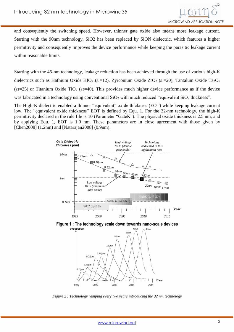
1995 2000 2005 2010 2015
0.1nm
1nm
10nm
Gate Dielectric Thickness (nm)
Year
0.25m
0.18m
0.13m
90nm 65nm
High voltage
MOS (double
gate oxide)
Technology
addressed in this
application note
22nm Low voltage
MOS (minimum
gate oxide)
SiO2 (r=3.9)
SiON (r=4.2-6.5)
HighK (r=7-20)
45nm 32nm
18nm 11nm
Figure 1 : The technology scale down towards nano-scale devices
1995 2000 2005 2010 2015
Production
Year
0. 5m
0.18m
130nm
90nm
65nm
0.35m
0.25m
45nm 32nm
Figure 2 : Technology ramping every two years introducing the 32 nm technology

Introducing 32 nm technology in Microwind35
3
MICROWIND APPLICATION NOTE
www.microwind.net
khigh
khigh
SiO tEOT
2 (Equ. 1)
Where
SiO2 = dielectric permittivity of SiO2 (3.9, no unit)
high-k = High-K dielectric permittivity
thigh-k = High-K oxide thickness (m)
In the 32-nm technology node, most IC manufacturers use so called “HK-MG” gate stack, meaning a
combination of high-K dielectric and metal gate. IBM 32nm use Hafnium Oxide to obtain an EOT close to
1.0 nm, and Intel claims an EOT of 0.9 nm (9 Å).
At each lithography scaling, the linear dimensions are approximately reduced by a factor of 0.7, and the area
is reduced by factor of 2. Smaller cell sizes lead to higher integration density which has risen to nearly 2.8
million gates per mm2 in the 32-nm technology.
The integrated circuit market has been growing steadily for many years, due to ever-increasing demand for
electronic devices. The production of integrated circuits for various technologies over the years is illustrated
in Fig. 2. It can be seen that a new technology has appeared regularly every two years, with a ramp up close
to three years. The production peak is constantly increased, and similar trends should be observed for novel
technologies such as 32-nm (forecast peak in 2013).
2. Transistor performances in 32-nm technology
Key features
Several 32-nm processes have been introduced by various manufacturers [Arnaud2008], [Chen2008], [Diaz
2008], [Hasegawa2008], [Natarajan2008], addressing different types of applications: IBM 32-nm
technology is addressing low power applications such as mobile communication devices [Chen2008] while
Intel is targeting high-performance microprocessors [Natarajan2008].
Parameter Value
VDD (V) 0.8-1.1 V
Effective gate length (nm) 25-35
Ion N (µA/µm) at 1V 1000-1550
Ion P (µA/µm) at 1V 500-1210
Ioff N (nA/µm) 0.1-200
Ioff P (nA/µm) 0.1-100
Gate dielectric HfO2, SiON
Equivalent oxide thickness
(nm) 0.9-1.2
# of metal layers 6-11
Interconnect layer
permittivity K 2.4-3.0
Table 2: Key features of the 32 nm technology
Depending on the manufacturer, the transistor channels range from 25 nm to 35 nm in length (25 to 35 billionths of a meter). Some of the key features of the 32-nm technologies from various providers are given in Table 2. Compared to 45-nm technology, most 32-nm technologies offer:
Introducing 32 nm technology in Microwind35
4
MICROWIND APPLICATION NOTE
www.microwind.net
30 % increase in switching performance
30 % less power consumption
2 times higher density
X 2 reduction of the leakage between source and drain and through the gate oxide
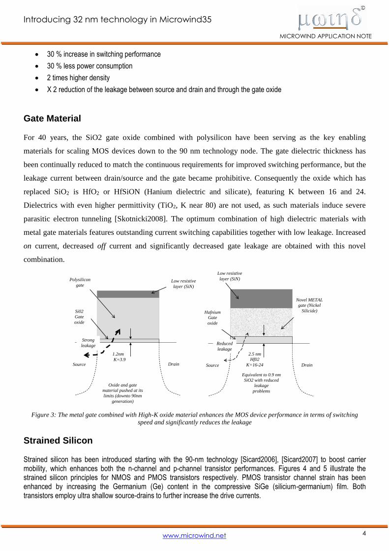
Gate Material
For 40 years, the SiO2 gate oxide combined with polysilicon have been serving as the key enabling
materials for scaling MOS devices down to the 90 nm technology node. The gate dielectric thickness has
been continually reduced to match the continuous requirements for improved switching performance, but the
leakage current between drain/source and the gate became prohibitive. Consequently the oxide which has
replaced SiO2 is HfO2 or HfSiON (Hanium dielectric and silicate), featuring K between 16 and 24.
Dielectrics with even higher permittivity (TiO2, K near 80) are not used, as such materials induce severe
parasitic electron tunneling [Skotnicki2008]. The optimum combination of high dielectric materials with
metal gate materials features outstanding current switching capabilities together with low leakage. Increased
on current, decreased off current and significantly decreased gate leakage are obtained with this novel
combination.
1.2nm
K=3.9 Source
Polysilicon
gate
Si02
Gate
oxide
Drain
2.5 nm
Hf02
K=16-24 Source
Novel METAL
gate (Nickel
Silicide) Hafnium
Gate
oxide
Drain
Oxide and gate
material pushed at its
limits (downto 90nm
generation)
Equivalent to 0.9 nm
SiO2 with reduced
leakage
problems
Low resistive
layer (SiN)
Low resistive
layer (SiN)
Strong
leakage Reduced
leakage
Figure 3: The metal gate combined with High-K oxide material enhances the MOS device performance in terms of switching
speed and significantly reduces the leakage
Strained Silicon
Strained silicon has been introduced starting with the 90-nm technology [Sicard2006], [Sicard2007] to boost carrier mobility, which enhances both the n-channel and p-channel transistor performances. Figures 4 and 5 illustrate the strained silicon principles for NMOS and PMOS transistors respectively. PMOS transistor channel strain has been enhanced by increasing the Germanium (Ge) content in the compressive SiGe (silicium-germanium) film. Both transistors employ ultra shallow source-drains to further increase the drive currents.

Introducing 32 nm technology in Microwind35
5
MICROWIND APPLICATION NOTE
www.microwind.net
Figure 4: Tensile strain generated by a silicon-nitride capping layer increases the distance between atoms underneath the gate,
which speeds up the electron mobility of n-channel MOS devices
Figure 5: Compressive strain to reduce the distance between atoms underneath the gate, which speeds up the hole mobility of p-
channel MOS devices
Let us assume that the silicon atoms form a regular lattice structure, inside which the carriers participating to the device current have to flow. In the case of electron carriers (NMOS), stretching the lattice (by applying tensile strain) allows the electrons to flow faster from the source to the drain, as depicted in Fig. 4. The mobility improvement exhibits a linear dependence on the tensile film thickness. In a similar way, compressing the lattice slightly speeds up the p-transistor, for which current carriers consist of holes (Fig. 5).
Intel has introduced a so-called “Replacement Metal Gate” (RMG) process flow in its 32 nm technology node [Natarajan2008] to further increase the channel strain, which consists of forming the Poly-Si gate first (Fig. 6a), then removing the gate (Fig. 6b) and then fabricating the Metal gate (Fig. 6c). The combination of reduced channel length, decreased oxide thickness and enhanced channel strain achieves a substantial gain in drive current for both nMOS and pMOS devices.
Moderate compressive
strain
SiGe
Poly
Gate
Gate
oxide
SiGe
Increased compressive
strain
SiGe
Gate
removed
Gate
oxide
SiGe
Increased compressive
strain
SiGe
Gate
oxide
SiGe
Metal
Gate
(a) (b) (c)
Figure 6: Increased p-channel MOS strain using a sacrificed poly gate and replacing it by metal gate [Natarajan2008]

Introducing 32 nm technology in Microwind35
6
MICROWIND APPLICATION NOTE
www.microwind.net
MOS types
Some 32-nm technologies comprise as much as 10 types of MOS devices (i.e. 20 devices in total). In Microwind, only three types of MOS devices (3 nMOS, 3 pMOS, 6 MOS devices in total) exist in the 32-nm technology :
► the low-leakage MOS is the default MOS device,
► the high-speed MOS has higher switching performance, thanks to a shorter effective channel length, at
the price of a much higher leakage.
► the high voltage MOS used for input/output interfacing. In Microwind’s cmos32nm rule file, the I/O supply
is 1.8 V. Some foundries also propose 2.5 V and 3.3 V interfacing. The main objective of the low leakage MOS is to reduce the Ioff current significantly, that is the small
current that flows between drain and source with a zero gate voltage (See Table 3). The price to pay is a
reduced Ion current. The designer has the choice of using high-speed MOS devices, which have high Ioff
leakages but large Ion drive currents. More details are provided in the following chapters.
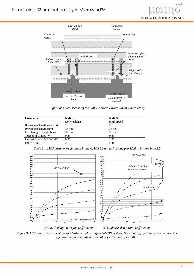
N-channel MOS device characteristics
Microwind version 3.5 is configured by default to the 32-nm technology. This technology uses a stack of high-k dielectric and metal gate (TiN). Layouts and cross-sections of two varieties of n-channel MOS devices are given in Fig. 7 and 8, where the high-speed device has a reduced channel length (26 nm instead of 32 nm). Although the high speed NMOS has a slightly shorter channel, it is drawn with exactly the same size as the low leakage NMOS. The nMOS gate is capped with a specific silicon nitride layer that induces lateral tensile channel strain to improve electron mobility. The pMOS strain is based on SiGe diffusion and Replacement Metal Gate (RMG). Key parameters for the MOS devices are shown in Table 3.
Figure 7: Layout of the low-leakage and high-speed MOS devices (Mos/allMosDevices.MSK). Dimensions are identical (2
lambda length).
Introducing 32 nm technology in Microwind35
7
MICROWIND APPLICATION NOTE
www.microwind.net
nMOS gate
Contact to
metal1
Metal1 layer
Shallow trench
isolation (STI)
32 nm effective
channel 26 nm effective
channel
Low leakage
nMOS
High speed
nMOS
High stress film to
induce channel
strain
High-k oxide
and TiN gate
Figure 8: Cross-section of the nMOS devices (Mos/allMosDevices.MSK)
Parameter NMOS
Low leakage
NMOS
High speed
Drawn gate length (lambda) 2 2
Drawn gate length (nm) 36 nm 36 nm
Effective gate length (nm) 32 nm 26 nm
Threshold voltage (V) 0.25 0.25
Ion (mA/µm) at VDD=1.0V 0.95 1.35
Ioff (nA/µm) 2 200
Table 3: nMOS parameters featured in the CMOS 32-nm technology provided in Microwind v3.5
Ion=0.95 mA
35% increase of the
maximum current
Low-leakage Ion
Ion=1.35 mA
(a) Low leakage W=1µm, Leff= 32nm (b) High speed W=1µm, Leff= 26nm
Figure 9: Id/Vd characteristics of the low leakage and high speed nMOS devices. Note that Ldrawn=36nm in both cases. The
effective length is significantly smaller for the high speed MOS

Introducing 32 nm technology in Microwind35
8
MICROWIND APPLICATION NOTE
www.microwind.net
Id/Vg for Vb=0, Vds=1 V
Ioff=2 nA
Vt=0.25 V
Ioff=200 nA
Vt=0.25 V
(a) low leakage MOS (Leff=32 nm) (b) high speed MOS (W=1 µm, Leff=26 nm)
Figure 10: Id/Vg characteristics (log scale) of the low leakage and high-speed nMOS devices
The I/V characteristics of the low-leakage and high-speed MOS devices (Figs. 9 and 10) are obtained using the MOS model BSIM4 (See [Sicard2007] for more information about this model). The I/V characteristics reported in Fig. 9 demonstrate that the low-leakage NMOS has a drive current capability of around 0.95 mA for W=1.0 µm at a voltage supply of 1.0 V (0.95 mA/µm). For the high speed NMOS, the effective channel length is slightly reduced (26 nm instead of 32 nm), to achieve a drive current around 1.35 mA/µm.
The drawback associated with this high current drive is the leakage current which rises from 2 nA/µm (low leakage NMOS) to 200 nA/µm (high speed NMOS), as seen in the Id/Vg curve at the X axis location corresponding to Vg= 0 V (Fig. 10).
P-channel MOS device characteristics
The PMOS drive current in CMOS 32-nm technology (Ion in Table 4) is around 600 µA/µm for the low-leakage MOS and up to 1000 µA/µm for the high-speed MOS. The leakage current is around 1 nA/µm for the low-leakage MOS and nearly 100 nA/µm for the high-speed device.
Parameter pMOS
Low leakage
pMOS
High speed
Drawn gate length (lambda) 2 2
Drawn gate length (nm) 36 36
Effective gate length (nm) 32 26
Threshold Voltage (V) -0.27 -0.25
Ion (mA/µm) at VDD=1.0V 0.60 1.00
Ioff (nA/µm) 1 100
Table 4: pMOS parameters featured by the 32-nm CMOS technology provided in Microwind v3.5
MOS Variability
One important challenge in nano-CMOS technology is process variability. The fabrication of millions of MOS devices at nano-scale induces a spreading in switching performances in the same IC. The most important parameters affected by process variability are the threshold voltage, the carrier mobility and the effective channel length. Variations are handled in Microwind using random values in a Gaussian distribution, which is expressed by the formulation of Equ. 2. An illustration of the variation in electron mobility (parameter U0) for nearly a thousand MOS device samples is reported in Fig. 11.

Introducing 32 nm technology in Microwind35
9
MICROWIND APPLICATION NOTE
www.microwind.net
2
2
2
)(
2
1
mx
ef
(Equ. 2)
where
f = probability density of the random variable (x axis in Fig. 11)
x = variable (y axis in Fig. 11)
= deviation
m = mean value
3.0
2.0
1.0
0.0
4.0
N-Channel MOS mobility (x 102 V. cm
-2)
MOS sample number
U0=320 V.cm-2
Probability
Value Deviation
Mean value
U0=320 V.cm-2
Figure 11: The extracted mobility of 1000 MOS samples shows an important variability around 320 V.cm-2
The effect of process variability on the MOS Ioff/Ion characteristics is plotted using the menu “Ioff vs. Ion”
under the “MOS I/V curve” menu (Fig. 12). It can be seen that the MOS devices have a wide variability in
performances. The 3 MOS types (low leakage, high speed, high voltage) are situated in well defined space in
the Ioff/Ion domain. The low leakage is in the middle (medium Ion, low Ioff), the high speed on the upper
right corner (high Ion, high Ioff), and the high voltage is at the lower left side of the graphics (low Ion, very
low Ioff). Note that the exact locations of the dots will change for each MOS characteristics plotted because
it is a random process.
Figure 12: Ioff/Ion calculated by Microwind on 100 samples of n-channel MOS with random distribution of VT, U0, and LINT
with a Gaussian distribution around the nominal value

Introducing 32 nm technology in Microwind35
10
MICROWIND APPLICATION NOTE
www.microwind.net
Very high Ion
current
Very low Ion
current
Very high
Ioff current
Very low Ioff
current
Average Ion
current
Average Ioff
current
Average trend in
this 32-nm
technology
High speed
Low
leakage
Figure 13: Finding compromises between high current drive and high leakage current
Concerning “worst case” and “best case”, notice that
Slow devices have high VT, low mobility U0 and long channel (LINT>0)
Fast devices have low VT, high mobility U0, and short channel (LINT<0)
3. Interconnects
Metal Layers
As seen in the palette (Fig. 14), the available metal layers in 32-nm technology range from metal1 to metal8.
The layer metal1 is situated at the lowest altitude, close to the active device, while metal8 is nearly 5 µm
above the silicon surface. Metal layers are labeled according to the order in which they are fabricated, i.e.
from the lower level (metal1) to the upper level (metal8).
Metal gate
introduced
starting at 45-
nm node
Figure 14: Microwind window with the palette of layers including 8 levels of metallization

Introducing 32 nm technology in Microwind35
11
MICROWIND APPLICATION NOTE
www.microwind.net
In Microwind, specific macros are accessible to ease the addition of contacts in the layout. These macros can
be found in the palette. As an example, you may instantiate a design-error free metal7/metal8 contact by
selecting metal8, followed by a click on the upper right corner icon in the palette. A metal7/metal8 contact is
depicted in Fig. 15. Additionally, access to complex stacked contacts is possible via the icon "complex
contacts" situated in the palette, in the second column of the second row. The screen shown in Fig. 16
appears when you click on this icon. By default it creates a contact from poly to metal1, and from metal1 to
metal2. Tick more boxes “between metals” to build more complex stacked contacts.
+ +
Metal7/Metal8 contact macro Metal7 Metal8 Via7
Figure 15: Access to contact macros between metal layers
Figure 16: Access to complex contact generator
Contact
poly/metal1..metal3
Contact poly-metal1-
..-metal8
Contact
P+diff/metal1..metal5
Contact
Metal5..metal8
Figure 17: Examples of layer connection using the complex contact command from Microwind (Interconnects /Contacts.MSK)

Introducing 32 nm technology in Microwind35
12
MICROWIND APPLICATION NOTE
www.microwind.net
Each metal layer is embedded into a low dielectric oxide (referred to as “interconnect layer permittivity K”
in Table 2), which isolates the layers from each other. A cross-section of a 32-nm CMOS technology is
shown in Fig. 17. In 32-nm technology, the layers metal1..metal4 have almost identical characteristics.
Concerning the design rules, the minimum width w of the interconnect is 3 (3 x 18 nm = 54 nm) and the
minimum spacing is 4 (4 x 18 nm = 72 nm). The metal pitch is 7 , that is 126 nm. Intel 32-nm CMOS
technology specifies a similar value (112 nm) [Natarajan2008], while IBM specifies 100 nm pitch for metal
1 and 200 nm for metal 2.
Figure 18: The Help > Design Rules menu of Microwind 3.5 gives details of the most important design rules
Layers metal5 and metal6 are a little thicker and wider, while layers metal7 and metal8 are significantly
thicker and wider, to drive high currents for power supplies. The design rules for metal8 are 15 (0.27 µm)
width, 20 (0.36 µm) spacing (See Help > Design Rules, Fig. 18).
Interconnect Resistance
At minimum width (3 x 18 nm = 54 nm), the interconnect resistance of the lower metal layers is around 7
/µm (Fig. 19), close to the value announced by Intel for metal 2 (8 ) [Natarajan2008]. Metal layers 1 to 3
have the same dimensions and design rules, and consequently the same resistance.

Introducing 32 nm technology in Microwind35
13
MICROWIND APPLICATION NOTE
www.microwind.net
Figure 19: Computing the wire resistance (Interconnects > metal1-5.MSK)
Note that the resistance computed in Microwind from 2D values gives a smaller value for lower metal layers than that
mentioned above. Click Analysis Interconnect Analysis with FEM. For metal 1 up to metal 3, a value of 3.4 /µm is obtained, assuming entirely copper interconnect (Fig. 20). The reason for getting a higher resistance in practice is that the real conductor is a combination of copper and higher-resistivity material mandatory for the interconnect process, which almost doubles the resistance (Fig. 21).
R=3.4 /µm
Figure 20: Extraction of the wire resistance using “Interconnect Analysis with FEM”
Introducing 32 nm technology in Microwind35
14
MICROWIND APPLICATION NOTE
www.microwind.net
In the computation of the
resistance, assuming the
entire layer to be copper
leads to 3.4 /µm
Metal 1
(copper)
Low K
oxide
3 (56 nm)
100
nm
In reality, only part of the
interconnect layer is made
up of copper, this leads to 7
/µm
Metal 1
(copper)
Low K
oxide
3 (56 nm)
100
nm High
resistance
layer
Figure 21: In reality, the lower metal layers feature a higher resistance, because the entire layer is not made up of low-resistivity
material
Interconnect Capacitance
An average value of 0.2 fF/µm is found in the literature for metal 2 capacitance. Some details are given by
Intel [Natarajan2008]. The usual setup consists of routing the lower and upper metal layers (resp. metal 1
and metal 3) at minimum pitch, as shown in Fig. 22, which is close to a realistic case. Consequently, the
metal2 capacitance is much higher compared to when it is routed alone without surrounding metal
interconnects. Note that the crosstalk capacitance, i.e. the capacitance between adjacent wires, is also quite
large at minimum pitch.
Figure 22: The interconnect capacitance is evaluated assuming that multiple wires are running below and above the layer under
consideration (Interconnects > Metal1-3.MSK)
Introducing 32 nm technology in Microwind35
15
MICROWIND APPLICATION NOTE
www.microwind.net
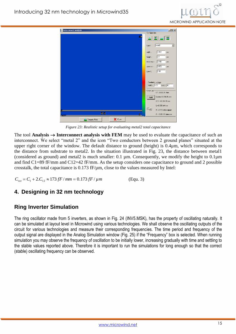
Figure 23: Realistic setup for evaluating metal2 total capacitance
The tool Analysis Interconnect analysis with FEM may be used to evaluate the capacitance of such an
interconnect. We select “metal 2” and the icon “Two conductors between 2 ground planes” situated at the
upper right corner of the window. The default distance to ground (height) is 0.4µm, which corresponds to
the distance from substrate to metal2. In the situation illustrated in Fig. 23, the distance between metal1
(considered as ground) and metal2 is much smaller: 0.1 µm. Consequently, we modify the height to 0.1µm
and find C1=89 fF/mm and C12=42 fF/mm. As the setup considers one capacitance to ground and 2 possible
crosstalk, the total capacitance is 0.173 fF/µm, close to the values measured by Intel:
µmfFmmfFCCCtot /173.0/173.2 121 (Equ. 3)
4. Designing in 32 nm technology
Ring Inverter Simulation
The ring oscillator made from 5 inverters, as shown in Fig. 24 (INV5.MSK), has the property of oscillating naturally. It can be simulated at layout level in Microwind using various technologies. We shall observe the oscillating outputs of the circuit for various technologies and measure their corresponding frequencies. The time period and frequency of the output signal are displayed in the Analog Simulation window (Fig. 25) if the “Frequency” box is selected. When running simulation you may observe the frequency of oscillation to be initially lower, increasing gradually with time and settling to the stable values reported above. Therefore it is important to run the simulations for long enough so that the correct (stable) oscillating frequency can be observed.

Introducing 32 nm technology in Microwind35
16
MICROWIND APPLICATION NOTE
www.microwind.net
Figure 24: Schematic diagram and layout of the ring oscillator used for simulation (INV5.MSK)
« warm-up phase » « steady-state »
Click « More »
to run more
simulation
Desired
simulation
duration
Click « Reset » to
restart simulation
from time = 0.0
Tick the
« Frequency »
box to view
frequency
Figure 25: The simulation always starts by a “warm-up” phase (1.0 ns). Click “More” to run more simulation (Inverter >
INV5.MSK)
Technol
ogy
Su
ppl
y
Oscillati
on
Chronograms
0.8 µm 5
V
0.76GH
z

Introducing 32 nm technology in Microwind35
17
MICROWIND APPLICATION NOTE
www.microwind.net
0.18 µm 2
V
7.5 GHz
32 nm 1.0
V
39 GHz
(high
speed
option)
Figure 26: Oscillation frequency improvement with the technology scale down (Inv5.MSK)
120 65 45 32
Technology generation (nm)
Gate delay
(ps)
1.0
10.0
100.0
45 nm: 7 ps Technology
described in this
work, 32 nm: 5 ps
90 180 22 17
High speed
Low leakage
120 nm: 12 ps
Memory point : 2.4 µm2
Memory point : 0.17 µm2
Figure 27: Comparison of gate delay for various technologies used in Microwind
The desired simulation duration can be selected from the drop down menu that appears under the “Time Scale” menu of the Simulation window. Remember to click the “Reset” button under the “Simulation” menu so that simulation results are refreshed for the selected duration. The time-domain waveforms of the outputs of the ring oscillator of Fig. 24 are reported in Fig. 26 for 0.8 µm, 0.18 µm and 32-nm technologies (high-speed option). Although the supply voltage (VDD) has been reduced (VDD is 5V in 0.8 µm, 2V in 0.18µm, and 1.0 V in 32-nm), the gain in frequency improvement is significant.
Use the command File Select Foundry to change the configuring technology. Sequentially select the
cmos08.RUL rule file which corresponds to the CMOS 0.8-µm technology, then cmos018.RUL rule file
(0.18µm technology), and eventually cmos32nm.RUL which configures Microwind to the CMOS 32-nm
technology. When you run the simulation, observe the change of VDD and the significant change in
oscillating frequency (Fig. 26).
In Fig. 27, we plot the gate delay per stage for various technologies, as computed using Microwind on a 5-
inverter ring oscillator. We divide the one-cycle delay by the number of stages

Introducing 32 nm technology in Microwind35
18
MICROWIND APPLICATION NOTE
www.microwind.net
to obtain the gate delay plotted in Y axis. We can observe that the improvement in switching delay with
technology scaling is significant although not impressive. Let us recall that the cell density has been
improved by a factor of 10 between the 120 nm generation and the 32 nm generation.
High Speed vs. Low leakage
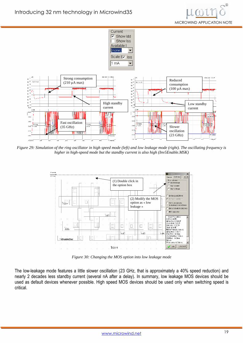
Let us consider the ring oscillator with an enable circuit, where one inverter has been replaced by a NAND gate to enable or disable oscillation (Inv5Enable.MSK). The schematic diagram of the oscillator and its layout implementation are shown in Fig. 28. We analyze its switching performance using high speed and low leakage MOS devices. The results are summarized in Fig. 28.
As shown in Fig. 29 the box "Scale I log" must be selected (ticked) to display the current in logarithmic scale. To select the “high speed” or “low leakage” MOS device click inside the option layer box in the layout which surrounds all the oscillator devices, and then select “high speed” or “low leakage” in the Navigator window. These actions are illustrated in Fig. 30. From the analog performances shown in Fig. 2928 we observe that the circuit works faster in the high speed mode (35 GHz) but consumes a significant amount of standby current, i.e. when it is off (around 100 nA).
Figure 28: The schematic diagram and layout of the ring oscillator used to compare the analog performances in high speed and
low leakage modes (INV5Enable.MSK)
Introducing 32 nm technology in Microwind35
19
MICROWIND APPLICATION NOTE
www.microwind.net
Strong consumption
(210 µA max)
High standby
current
Fast oscillation
(35 GHz) Slower
oscillation
(23 GHz)
Low standby
current
Reduced
consumption
(100 µA max)
Figure 29: Simulation of the ring oscillator in high speed mode (left) and low leakage mode (right). The oscillating frequency is
higher in high-speed mode but the standby current is also high (Inv5Enable.MSK)
(1) Double click in
the option box
(2) Modify the MOS
option as « low
leakage »
Figure 30: Changing the MOS option into low leakage mode
The low-leakage mode features a little slower oscillation (23 GHz, that is approximately a 40% speed reduction) and nearly 2 decades less standby current (several nA after a delay). In summary, low leakage MOS devices should be used as default devices whenever possible. High speed MOS devices should be used only when switching speed is critical.
Introducing 32 nm technology in Microwind35
20
MICROWIND APPLICATION NOTE
www.microwind.net
Simulation of Process Variations (PVT)
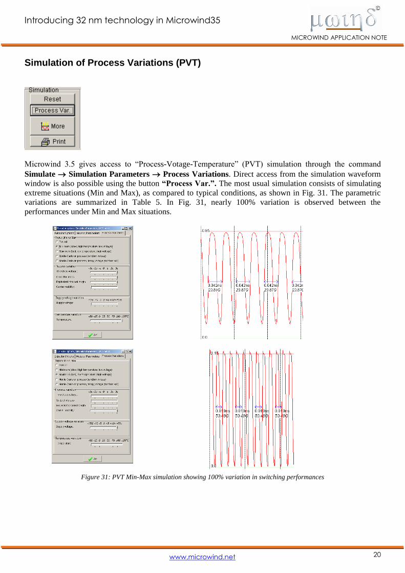
Microwind 3.5 gives access to “Process-Votage-Temperature” (PVT) simulation through the command
Simulate Simulation Parameters Process Variations. Direct access from the simulation waveform
window is also possible using the button “Process Var.”. The most usual simulation consists of simulating
extreme situations (Min and Max), as compared to typical conditions, as shown in Fig. 31. The parametric
variations are summarized in Table 5. In Fig. 31, nearly 100% variation is observed between the
performances under Min and Max situations.
Figure 31: PVT Min-Max simulation showing 100% variation in switching performances
Introducing 32 nm technology in Microwind35
21
MICROWIND APPLICATION NOTE
www.microwind.net
Notice that
In Min situation, VT is high, mobility U0 is low and the channel is long (LINT>0). The supply
is minimum and the temperature is maximum.
In Max situation, VT is low, mobility U0 is high and the channel is short (LINT<0). The supply
is maximum and the temperature is minimum.
Parameter
class
Parameter Symbol
(BSIM4)
Unit Min
(32-nm)
Typ
(32-nm)
Max
(32-nm)
Process Threshold
Voltage
VT V 0.30 0.25 0.20
Mobility U0 cm.V-2 500 600 700
Channel length
reduction
LINT m 2e-9 0 -2e-9
Voltage Supply VDD V 0.85 1.0 1.15
Temperature Temperature TEMP °C 125 27 -50
Table 5: Variation of process parameters
6-transistor static RAM
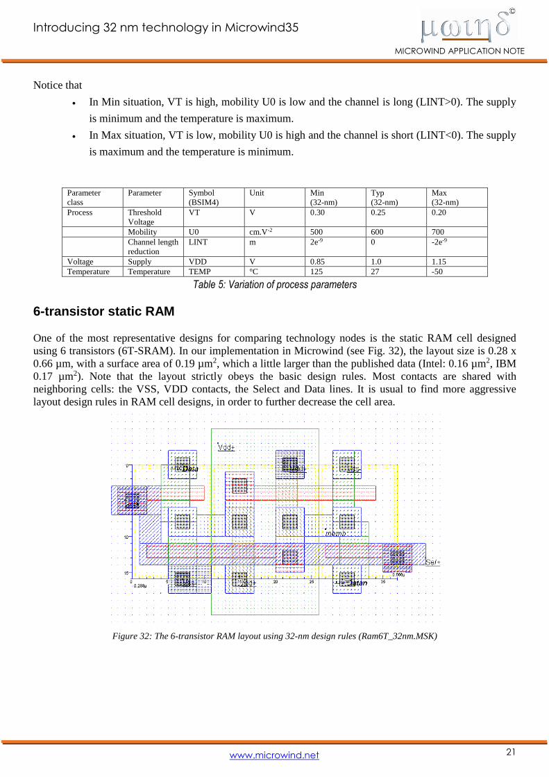
One of the most representative designs for comparing technology nodes is the static RAM cell designed
using 6 transistors (6T-SRAM). In our implementation in Microwind (see Fig. 32), the layout size is 0.28 x
0.66 µm, with a surface area of 0.19 µm2, which a little larger than the published data (Intel: 0.16 µm2, IBM
0.17 µm2). Note that the layout strictly obeys the basic design rules. Most contacts are shared with
neighboring cells: the VSS, VDD contacts, the Select and Data lines. It is usual to find more aggressive
layout design rules in RAM cell designs, in order to further decrease the cell area.
Figure 32: The 6-transistor RAM layout using 32-nm design rules (Ram6T_32nm.MSK)

Introducing 32 nm technology in Microwind35
22
MICROWIND APPLICATION NOTE
www.microwind.net
5. Conclusions
This application note has illustrated the trends in CMOS technology and introduced the 32-nm technology
generation, based on technology information available from integrated circuit manufacturers. A set of
specific topics has been addressed, including the new gate dielectric, gate stack and the strained silicon
technique for enhanced mobility, the 8-metal interconnect back-end process and the 32-nm process variants.
N-channel and P-channel MOS device characteristics have been presented, as well as a comparative study of
a ring inverter oscillator for various technology nodes. Finally, performance of the ring oscillator in the high
speed and low leakage modes have been compared, with the impact on speed and leakage current. Future
work will concern the 22-nm technology node, under preparation for an industrial production in 2012.
References
[Arnaud2008] F. Arnaud et al, “32nm General Purpose Bulk CMOS Technology for High Performance Applications at Low Voltage”, IEDM Tech Dig., 2008, pp. 1-4.
[Chen2008] C X. Chen et al, “A Cost Effective 32nm High-K/ Metal Gate CMOS Technology for Low Power Applications with Single-Metal/Gate-First Process”, Symposium on VLSI Technology Digest of Technical Papers, 2008, pp. 88-89.
[Common2009] The Common Platform technology model is focused on 90-nm downto 32-nm technology http://www.commonplatform.com
[Diaz2008] C. H. Diaz et al, “32nm Gate-First High-k/Metal-Gate Technology for High Performance Low Power Applications”, IEDM Tech Dig., 2008, pp. 1-4.
[Hasegawa2008] S. Hasegawa et al, “A Cost-Conscious 32nm CMOS Platform Technology with Advanced Single Exposure Lithography and Gate-First Metal Gate/High-K Process”, IEDM Tech Dig., 2008, pp. 1-3.
[ITRS2009] The ITRS roadmap for semiconductors may be downloaded from http://www.itrs.net
[Natarajan2008] S. Natarajan et al, “A 32nm Logic Technology Featuring 2nd-Generation High-k + Metal-Gate Transistors, Enhanced Channel Strain and 0.171µm2 SRAM Cell Size in a 291Mb Array”, IEDM Tech Dig., 2008, pp. 1-3.
[Sicard2006] E. Sicard and S. M. Aziz, “Introducing 65-nm technology in Microwind3”, software application note, July 2006, www.microwind.org
[Sicard2007] E. Sicard, S. Ben Dhia “Basic CMOS cell design”, McGraw Hill, 450 pages, international edition 2007 – ISBN 9780071488396
[Sicard2008] E. Sicard and S. M. Aziz, “Introducing 45-nm technology in Microwind3”, software application note, July 2008, www.microwind.org
[Sicard2009] E. Sicard “Microwind User’s Manual, lite version 3.5”, INSA editor, 2009, www.microwind.org.
[Skotnicki2008] Skotnicki, T. and all, “Innovative Materials, Devices, and CMOS Technologies for Low-Power Mobile Multimedia”, IEEE Trans. Electron Device, Vol 55, N°1, pp 96-130