Embed Size (px)
Citation preview

INTRO TO TDM AND BUM
TDM – Top Down Manufacturing
BUM – Bottom Up Manufacturing

TOP DOWN MANUFACTURING
• Materials modified
• Cutting, drilling, milling
• Machinery used
• Many steps needed
• Primary method in integrated circuits industry
BOTTOM UP MANUFACTURING
• Similar to way nature builds objects
• Self-assembly
• Atomic force microscope
• The future of nano-manufacturing?
MOORE’S LAW
• Integrated circuits (ICs) are electronic circuits on a single piece of silicon
• Circuits on ICs are made from many transistors• Since 1965 trend is for the number of transistors
per integrated circuit to double every two years• In 1965 there were 30 transistors per chip• Today, more than 1 billion transistors per chip

MOORE’S LAW
TDM IN SEMICONDUCTOR MANUFACTURING
• Transistors are semiconductor devices• Transistors connected together form circuits• Integrated circuits consists of many
transistors• Many ICs built simultaneously on silicon
wafers• Transistors are built first, then
interconnected• ICs are built in a chip fab
TDM IN SEMICONDUCTOR MANUFACTURING
• ICs are built layer by layer
• Process steps include:
• Wafer photolithography ion implant
• Deposition metallization
• Steps repeated many times for each IC

PHOTOLITHOGRAPHY
• Mask is high quality glass
• Mask has areas marked to block transmission of light
• One mask for every layer of the IC
• Photoresist covers IC
• Ultraviolet light shines through mask onto photoresist
• Photoresist affected by light

PHOTOLITHOGRAPHY

PHOTOLITHOGRAPHY
• Photolithography defines transistor size
• Part of process is to reduce image on mask
• Transistors made of several features
• Feature size defines how small transistors are
• Smallest feature size currently is 45nm

PROBLEM WITH TDM
• TDM processing reaching physical limits
• Difficult to reduce mask images to smaller and smaller levels
• Requires shorter wave length light (X-rays)
• Requires more sophisticated optical systems to reduce images
• This are expensive and technically challenging

Bottom Up Manufacturing
• Possible way to continue Moore’s Law progress
• Build features one atom at a time
• Use forces of nature to accomplish this
• No machining necessary
• Requires proper environmental conditions

AFM
• Atomic force microscope
• Can image atoms
• Can move atoms
• Forces between atom and ATM tip interact
• Measurement of forces used to produce image of atom or to manipulate atoms
• IBM logo made from xenon atoms in 1990
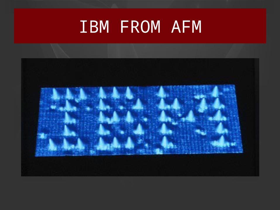
IBM FROM AFM

SELF-ASSEMBLY
• Self-assembly occurs naturally
• Smaller features are created
• Smaller features combine to produce larger features
• Combinations occur until macro structure is built

SELF-ASSEMBLY

SELF-ASSEMBLY

SELF-ASSEMBLY IN SOAP
• Soap bubbles consist od soap molecules and water molecules
• Soap molecule ends react differently with water
• Hydrophili end links with water easily
• Hydrophobic end will not link with water
• Monolayers form to create bubble wall
• Wall is soap-water-soap

SELF-ASSEMBLY IN SOAP
• http://nanopedia.case.edu/NWPage.php?page=soap.bubbles
• http://www.nanooze.org/english/articles/article14_selfassembly.html
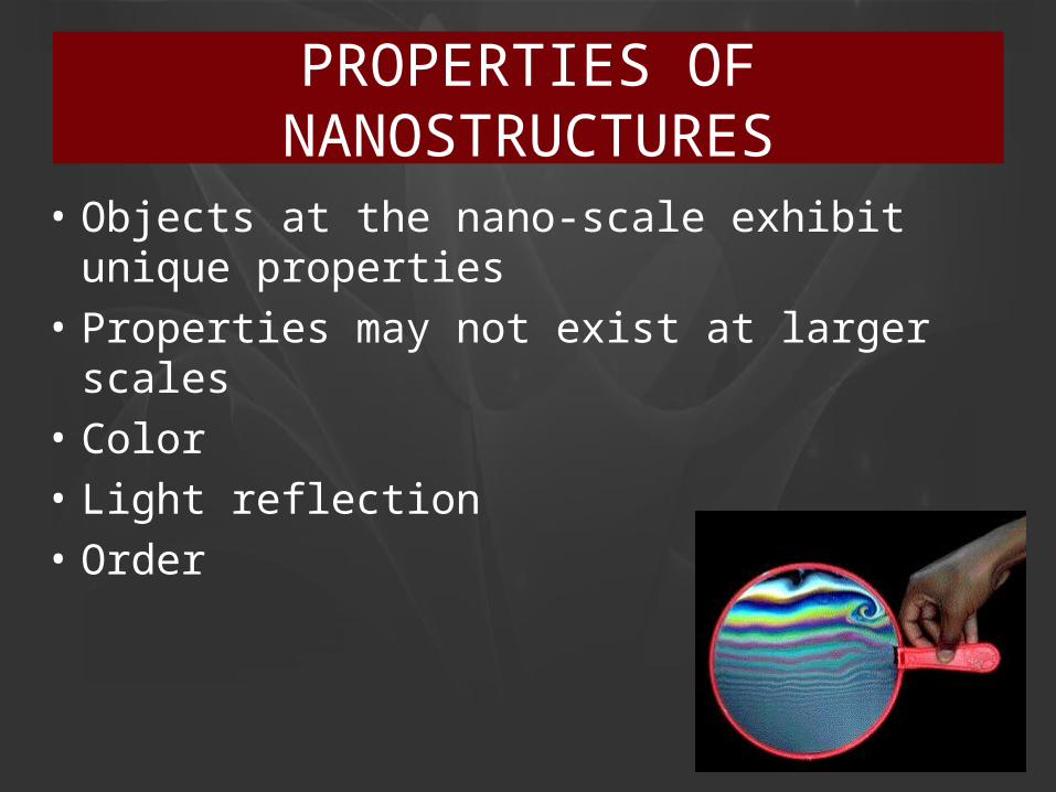
PROPERTIES OF NANOSTRUCTURES
• Objects at the nano-scale exhibit unique properties
• Properties may not exist at larger scales
• Color
• Light reflection
• Order

COLOR PROPERTIES OF SOAP
• http://www.exploratorium.edu/ronh/bubbles/bubble_colors.html
• http://www.exploratorium.edu/ronh/bubbles/bubble_meets_bubble.html