Embed Size (px)
Citation preview

International Technology Roadmap for Semiconductors
Dave Armstrong – Advantest
Ira Feldman – Feldman Engineering
Marc Loranger - FormFactor

Overview
• Who are we?
• Why a roadmap?
• What is the purpose?
• Example Trends
• How can you help?
• Summary
Armstrong-Feldman-Loranger

ITRS Team
• Three of us are presenting today – Dave (Advantest) – Test TWG Chairman
– Marc (FormFactor) - Probing Team Leader
– Ira (Feldman Engineering) - Communications
Armstrong-Feldman-Loranger
• Test Working Group – More than 70 professionals
– More than 45 companies
• Large ITRS Team – More than a 1,000 professionals
– Over 100 companies
– 16 Working Groups
Why a Roadmap? • The ITRS is generated each year to report on the
technological fundamentals of our industry.
• In addition, by extrapolating on the trends inherent in today’s semiconductor technology we identify disconnects and discuss possible approach to overcome these challenges.
• Through this effort we all can get a better sense of the path of least resistance and align our plans and standards in a fashion which is most likely to succeed.
Armstrong-Feldman-Loranger

What Is and What Isn’t the ITRS
Armstrong-Feldman-Loranger
What Is the ITRS
– The combined expert opinion by this team.
– The results of many different technology models.
– A “best guess” of where the industry is heading for the next 15 years.
– A highlighting of disconnects and significant challenges.
What Isn’t the ITRS
– It doesn’t implement or define Moore’s Law – it just tries to predict how things will likely trend.
– A commitment from the involved companies to do what is reported.
– Specific solutions or prescriptive.

ITRS Process
Armstrong-Feldman-Loranger
Working Group Discusses
Challenges
Sub-Team Analyzes
Implications
Implications Discussed with Other
Working Groups
Sub-Team Reconciles Feedback from Other
Groups
Entire Team Publishes a New Roadmap Yearly

Test Complexity Drivers • Device trends
– Increasing device interface bandwidth – Increasing device integration (SoC, SiP, MCP, 3D packaging)
• Homogenous & heterogeneous dies functional disaggregation
– Integration of emerging and non-digital CMOS technologies – Complex package electrical and mechanical characteristics – Device characteristics beyond one sided stimulus/response
model – 3 Dimensional silicon - multi-die and Multi-layer – Integration of non-electrical devices (optical, MEMS, etc.) – Fault Tolerant Architectures and Protocols
• Industry trends – 450 mm wafer transition
7

Date = When in Production
Armstrong-Feldman-Loranger
ITRS 2013 Overview: Figure 1a A Typical Technology Production “Ramp” Curve (within an established wafer generation)

Wafer Probe Requirements Parameter MPU &
ASIC DRAM NAND RF &
AMS LCD
Drivers CIS
Wirebond – inline pad pitch X X X X X X
Wirebond – stagger pad pitch X X X
Bump – array pitch X X
I/O Pad Size X X X X X
Wafer Test Frequency X X X X
High Speed I/O Frequency X X X
Wirebond - Probe Tip Diameter X X X X X X
Bump – Probe Tip Diameter X X
Probe Force X X X X X
Probe (Active) Area X X X X X X
# of Probes per Touchdown X X X X X X
Maximum Current / Probe X X X X X
Maximum Resistance X X X
Armstrong-Feldman-Loranger

Parallelism Trend
Armstrong-Feldman-Loranger

SoC (MPU) Bump Pitch Trend
• Technology shift in 2012
Armstrong-Feldman-Loranger
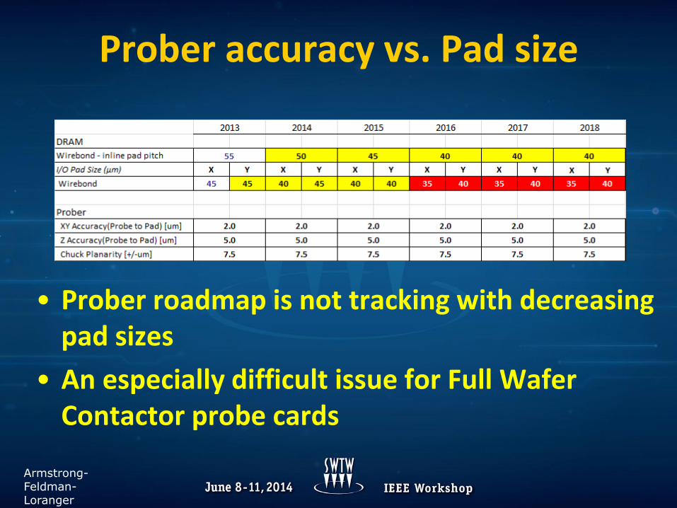
Prober accuracy vs. Pad size
• Prober roadmap is not tracking with decreasing pad sizes
• An especially difficult issue for Full Wafer Contactor probe cards
Armstrong-Feldman-Loranger

Next Challenges for Probe Cards
• Decreasing pad / bump sizes and pitch
• Increasing parallelism SoC and Memory
• Increased use of die for MCP, 2.5D and 3D integration will drive more wafer sort
• 2 sided probing
• Testing stacked devices (e.g. HBM)
• MEMS and sensor sort test
• Cost of test as a driver
Armstrong-Feldman-Loranger

Opportunities for Involvement!
• Download ITRS data at:
http://www.itrs.net/Links/2013ITRS/Home2013.htm
• Provide feedback on test data at:
http://j.mp/ITRSTestSurvey
• Sign up:
Armstrong-Feldman-Loranger

Summary
• Great Tool
– Well accepted independent industry wide reference
• Challenges
– Requires broad-based inputs
– Track potential disruptive technology
• Help Us
– Get Involved!
Armstrong-Feldman-Loranger