Embed Size (px)
Citation preview

Research Article Impact Factor: 4.226 ISSN: 2319-507X Abirami A, IJPRET, 2014; Volume 3 (4): 138-148 IJPRET
Available Online at www.ijpret.com
138
INTERNATIONAL JOURNAL OF PURE AND APPLIED RESEARCH IN ENGINEERING AND
TECHNOLOGY A PATH FOR HORIZING YOUR INNOVATIVE WORK
SIMULATION ON THREE AXIS MEMS ACCELEROMETER
ABIRAMI A
Assistant Professor/ECE Department/Apollo Engineering College.
Accepted Date: 22/11/2014; Published Date: 01/12/2014
\
Abstract: In developing Micro Electro Mechanical Systems (MEMS), Finite Element Analysis (FEA) is usually relied upon to study these micro-structures in determining stress, deformation, resonance, temperature distribution, electromagnetic interference, and electrical properties. With this kind of approach, the performance of the devices can be easily expanded, as well as reducing the time and cost of MEMS production. Instead of constructing the MEMS devices in the laboratory, the simulation of MEMS using FEA programs like ANSYS, ABAQUS, LS-DYNA, INTELLISUITE, etc. in that INTELLISUITE now boasts the widest range of features available in a MEMS tool, and remains unsurpassed in its simulation capabilities, robustness and ease of use. The conventional MEMS accelerometers are used to sense two dimensional acceleration of the vehicle. Due to that car airbag can deploy early or later not in an exact time, hence it will not protect the accidental damage. This work focuses on the modeling of three axis MEMS accelerometer with INTELLISUITE software and recognition of motion in all three axes is noted. Keywords: Micro Electro Mechanical Systems (MEMS), Accelerometer, Intellisuite
Corresponding Author: MR. A. ABIRAMI
Access Online On:
www.ijpret.com
How to Cite This Article:
Abirami A, IJPRET, 2014; Volume 3 (4): 138-148
PAPER-QR CODE
Research Article Impact Factor: 4.226 ISSN: 2319-507X Abirami A, IJPRET, 2014; Volume 3 (4): 138-148 IJPRET
Available Online at www.ijpret.com
139
INTRODUCTION
Micro-Electro-Mechanical Systems, or MEMS, is a technology that in its most general form can
be defined as miniaturized mechanical and electro-mechanical elements (i.e., devices and
structures) that are made using the techniques of micro fabrication. The critical physical
dimensions of MEMS devices can vary from well below one micron on the lower end of the
dimensional spectrum, all the way to several millimetres. Likewise, the types of MEMS devices
can vary from relatively simple structures having no moving elements, to extremely complex
electromechanical systems with multiple moving elements under the control of integrated
microelectronics.
The one main criterion of MEMS is that there are at least some elements having some sort of
mechanical functionality whether or not these elements can move. The term used to define
MEMS varies in different parts of the world. In the United States they are predominantly called
MEMS while in some other parts of the world they are called “Microsystems Technology” or
“micro machined devices”.
While the functional elements of MEMS are miniaturized structures, sensors, actuators, and
microelectronics, the most notable (and perhaps most interesting) elements are the micro
sensors and micro actuators. Micro sensors and micro actuators are appropriately categorized
as “transducers”, which are defined as devices that convert energy from one form to another.
In the case of micro sensors, the device typically converts a measured mechanical signal into an
electrical signal.
NEED FOR MINIATURATION
Miniaturization (Miniaturisation) is the creation of ever-smaller scales for mechanical, optical,
and electronic products and devices. Miniaturization is a continuing trend in the production of
such devices. Items which take up less space are more desired than items which are bigger and
bulkier because they are easier to carry, easier to store, and much more convenient to use.
FEATURE OF MEMS
Each of the three basic Microsystems technology processes we have seen, bulk
micromachining, sacrificial surface micromachining, and micro moulding/LIGA, employs a
different set of capital and intellectual resources. MEMS manufacturing firms must choose
which specific Microsystems manufacturing techniques.

Research Article Impact Factor: 4.226 ISSN: 2319-507X Abirami A, IJPRET, 2014; Volume 3 (4): 138-148 IJPRET
Available Online at www.ijpret.com
140
MEMS technology has the potential to change our daily lives as much as the computer has.
However, the material needs of the MEMS field are at a preliminary stage. A thorough
understanding of the properties of existing MEMS materials is just as important as the
development of new MEMS materials.
Future MEMS applications will be driven by processes enabling greater functionality through
higher levels of electronic-mechanical integration and greater numbers of mechanical
components working alone or together to enable a complex action. Future MEMS products will
demand higher levels of electrical-mechanical integration and more intimate interaction with
the physical world. The high up-front investment costs for large-volume commercialization of
MEMS will likely limit the initial involvement to larger companies in the IC industry. Advancing
from their success as sensors, MEMS products will be embedded in larger non-MEMS systems,
such as printers, automobiles, and biomedical diagnostic equipment, and will enable new and
improved systems
ADVANTAGE OF MEMS
MEMS are devices that integrate mechanical elements, sensors, actuators, and electronics on a
common silicon substrate. Many typically have dimensions in the 1 micron to 100 micron range.
They have proven to be a key enabling technology of developments in areas such as
transportation, telecommunications and health care, but the range of MEMS applications
covers nearly every field.
The most significant advantage of MEMS is their ability to communicate easily with electrical
elements in semiconductor chips. Other advantages include small size, lower power
consumption, lower cost, increased reliability and higher precision.
EXPERIMENTS
Open the 3D builder module. The 3D Builder window will open as shown below
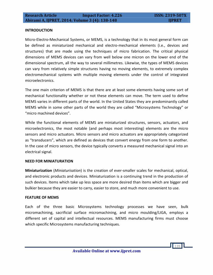
Creation of level 1
Click on the Add Rectangle button in the left pane and then draw four rectangular supports
(anchors) at the mid points of all sides and define the height as given in the Fig 1 below
Research Article Impact Factor: 4.226 ISSN: 2319-507X Abirami A, IJPRET, 2014; Volume 3 (4): 138-148 IJPRET
Available Online at www.ijpret.com
141
Figure 1 creation of level 1
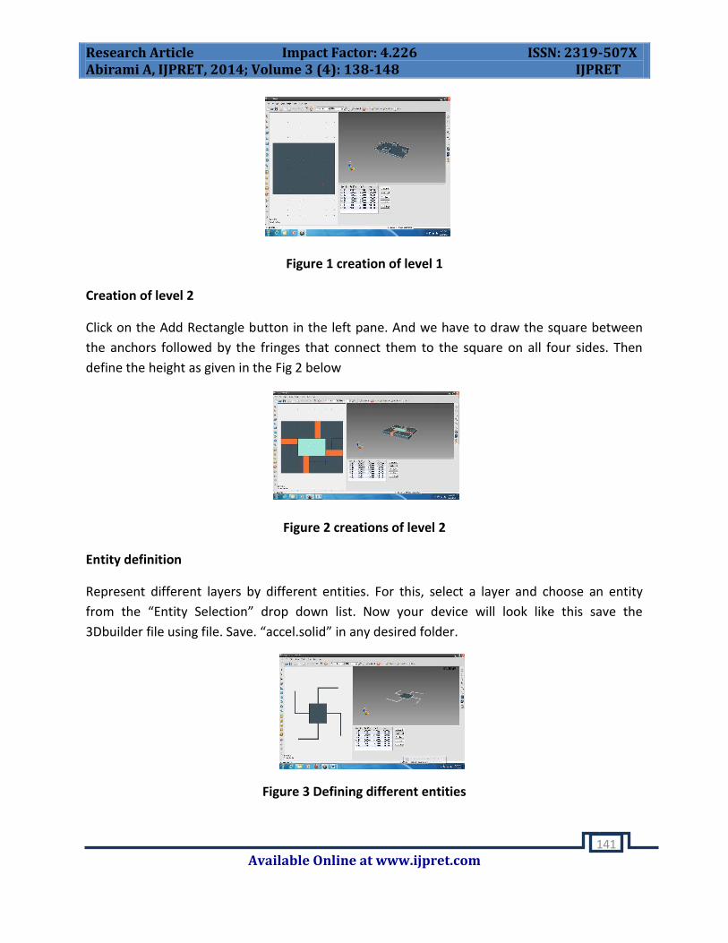
Creation of level 2
Click on the Add Rectangle button in the left pane. And we have to draw the square between
the anchors followed by the fringes that connect them to the square on all four sides. Then
define the height as given in the Fig 2 below
Figure 2 creations of level 2
Entity definition
Represent different layers by different entities. For this, select a layer and choose an entity
from the “Entity Selection” drop down list. Now your device will look like this save the
3Dbuilder file using file. Save. “accel.solid” in any desired folder.
Figure 3 Defining different entities

Research Article Impact Factor: 4.226 ISSN: 2319-507X Abirami A, IJPRET, 2014; Volume 3 (4): 138-148 IJPRET
Available Online at www.ijpret.com
142
Analysis
To export the file to the analysis module, select file export to analysis module. Select the
two check boxes that request for mesh verification and click on the “check” button as
shown in the Fig 4 given below
Figure 4 Validate mesh dialog box
Then click on thermo electromechanical module option as shown in Fig 5 below
Figure 5 TEM Analysis modules
Save the analysis file as “accelanalyse.save” The thermo electromechanical analysis module
will be displayed as shown in Fig 6 below
Figure 6 TEM Simulation Windows

Research Article Impact Factor: 4.226 ISSN: 2319-507X Abirami A, IJPRET, 2014; Volume 3 (4): 138-148 IJPRET
Available Online at www.ijpret.com
143
Meshing
To create a mesh for a job, Mesh…Auto Mesh option and give a value of 10 in the auto
mesh dialog box as shown in Fig 7.
Figure 7 Auto mesh dialog box
Simulation settings
To define simulation settings, select Simulation …Simulation settings from the menu and
choose “Static” option and select Stress/Displacement option and click OK
Figure 8 Simulation setting window
Material selection
To import material properties, select Materials. Check/Modify from the menu and then
select the required entity for applying the material properties. Select the desired material
and also change the required property of the chosen material by selecting a common
material for them as shown in the screen shot. Select the button level 0 and choose its
property as that of Si_Bulk_General material as shown in the Fig 9.
Research Article Impact Factor: 4.226 ISSN: 2319-507X Abirami A, IJPRET, 2014; Volume 3 (4): 138-148 IJPRET
Available Online at www.ijpret.com
144
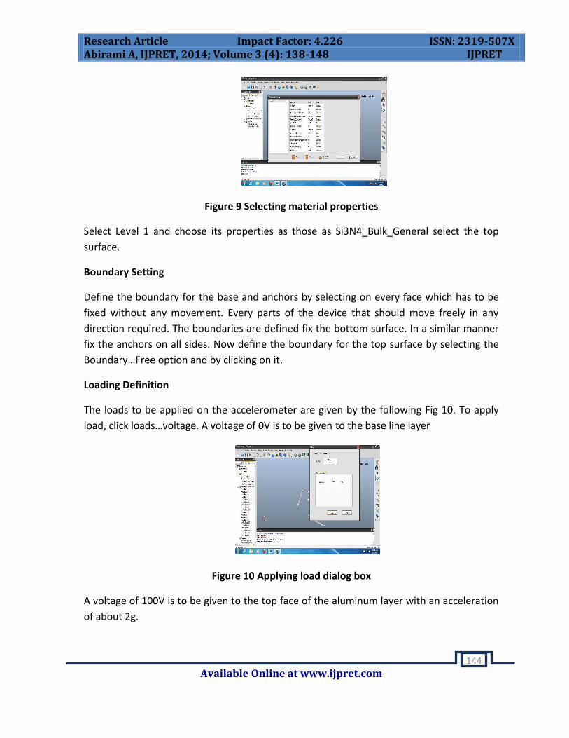
Figure 9 Selecting material properties
Select Level 1 and choose its properties as those as Si3N4_Bulk_General select the top
surface.
Boundary Setting
Define the boundary for the base and anchors by selecting on every face which has to be
fixed without any movement. Every parts of the device that should move freely in any
direction required. The boundaries are defined fix the bottom surface. In a similar manner
fix the anchors on all sides. Now define the boundary for the top surface by selecting the
Boundary…Free option and by clicking on it.
Loading Definition
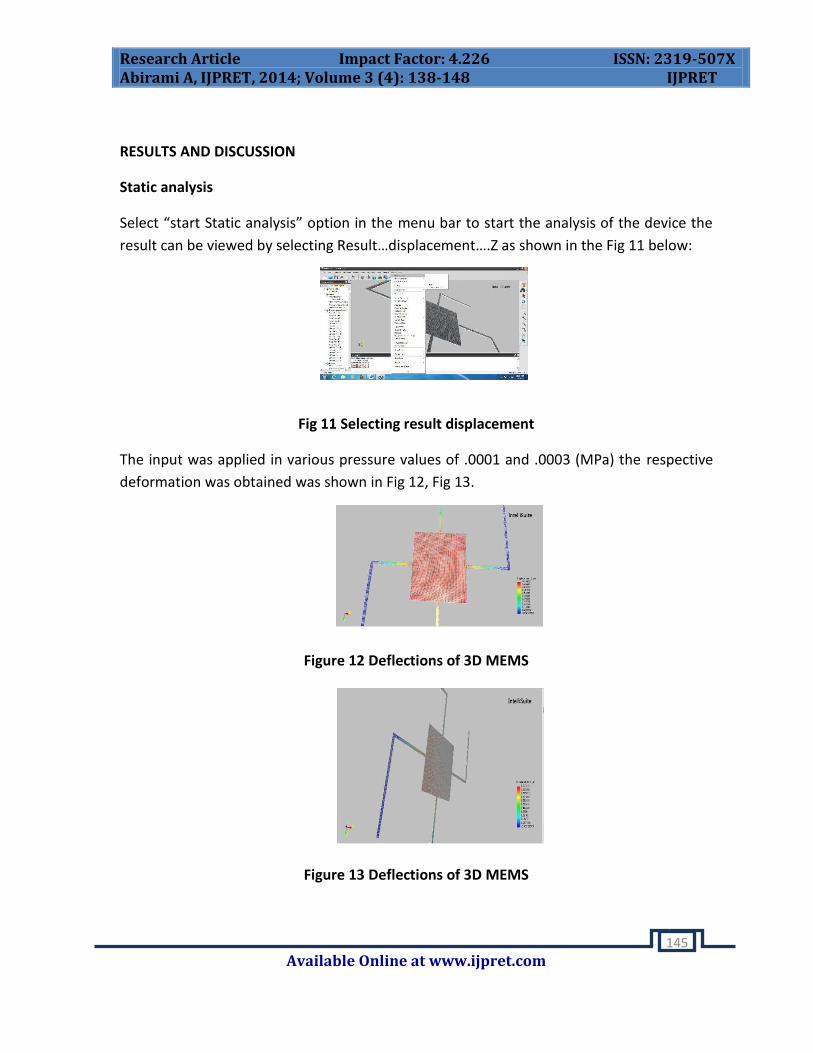
The loads to be applied on the accelerometer are given by the following Fig 10. To apply
load, click loads…voltage. A voltage of 0V is to be given to the base line layer
Figure 10 Applying load dialog box
A voltage of 100V is to be given to the top face of the aluminum layer with an acceleration
of about 2g.
Research Article Impact Factor: 4.226 ISSN: 2319-507X Abirami A, IJPRET, 2014; Volume 3 (4): 138-148 IJPRET
Available Online at www.ijpret.com
145
RESULTS AND DISCUSSION
Static analysis
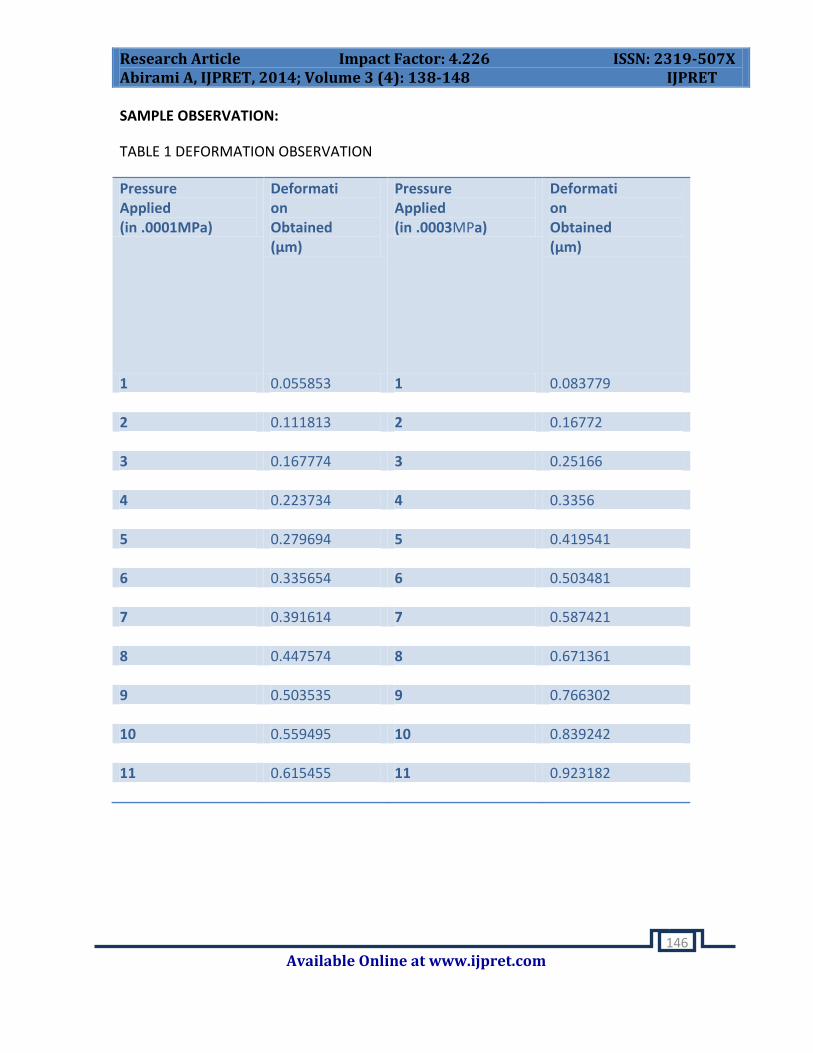
Select “start Static analysis” option in the menu bar to start the analysis of the device the
result can be viewed by selecting Result…displacement….Z as shown in the Fig 11 below:
Fig 11 Selecting result displacement
The input was applied in various pressure values of .0001 and .0003 (MPa) the respective
deformation was obtained was shown in Fig 12, Fig 13.
Figure 12 Deflections of 3D MEMS
Figure 13 Deflections of 3D MEMS
Research Article Impact Factor: 4.226 ISSN: 2319-507X Abirami A, IJPRET, 2014; Volume 3 (4): 138-148 IJPRET
Available Online at www.ijpret.com
146
SAMPLE OBSERVATION:
TABLE 1 DEFORMATION OBSERVATION
Pressure Applied (in .0001MPa)
Deformati on Obtained (µm)
Pressure Applied (in .0003MPa)
Deformati on Obtained (µm)
1 0.055853 1 0.083779 2 0.111813 2 0.16772 3 0.167774 3 0.25166 4 0.223734 4 0.3356 5 0.279694 5 0.419541 6 0.335654 6 0.503481 7 0.391614 7 0.587421 8 0.447574 8 0.671361 9 0.503535 9 0.766302 10 0.559495 10 0.839242 11 0.615455 11 0.923182
Research Article Impact Factor: 4.226 ISSN: 2319-507X Abirami A, IJPRET, 2014; Volume 3 (4): 138-148 IJPRET
Available Online at www.ijpret.com
147
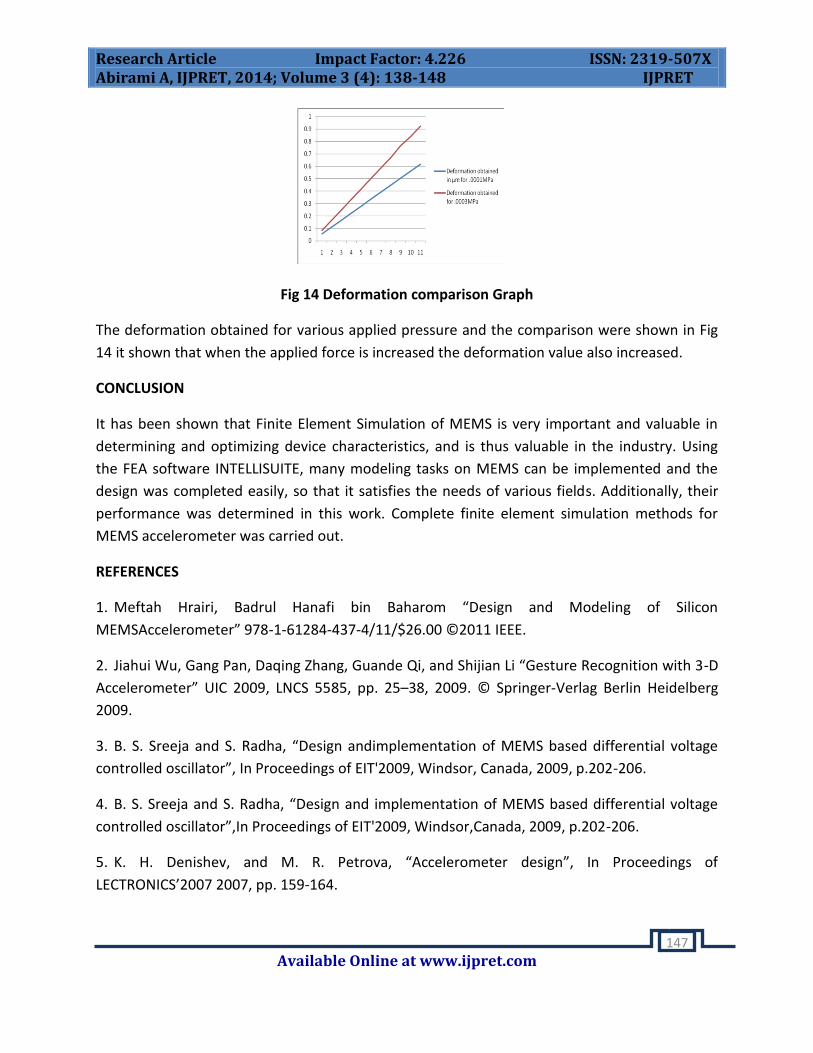
Fig 14 Deformation comparison Graph
The deformation obtained for various applied pressure and the comparison were shown in Fig
14 it shown that when the applied force is increased the deformation value also increased.
CONCLUSION
It has been shown that Finite Element Simulation of MEMS is very important and valuable in
determining and optimizing device characteristics, and is thus valuable in the industry. Using
the FEA software INTELLISUITE, many modeling tasks on MEMS can be implemented and the
design was completed easily, so that it satisfies the needs of various fields. Additionally, their
performance was determined in this work. Complete finite element simulation methods for
MEMS accelerometer was carried out.
REFERENCES
1. Meftah Hrairi, Badrul Hanafi bin Baharom “Design and Modeling of Silicon
MEMSAccelerometer” 978-1-61284-437-4/11/$26.00 ©2011 IEEE.
2. Jiahui Wu, Gang Pan, Daqing Zhang, Guande Qi, and Shijian Li “Gesture Recognition with 3-D
Accelerometer” UIC 2009, LNCS 5585, pp. 25–38, 2009. © Springer-Verlag Berlin Heidelberg
2009.
3. B. S. Sreeja and S. Radha, “Design andimplementation of MEMS based differential voltage
controlled oscillator”, In Proceedings of EIT'2009, Windsor, Canada, 2009, p.202-206.
4. B. S. Sreeja and S. Radha, “Design and implementation of MEMS based differential voltage
controlled oscillator”,In Proceedings of EIT'2009, Windsor,Canada, 2009, p.202-206.
5. K. H. Denishev, and M. R. Petrova, “Accelerometer design”, In Proceedings of
LECTRONICS’2007 2007, pp. 159-164.

Research Article Impact Factor: 4.226 ISSN: 2319-507X Abirami A, IJPRET, 2014; Volume 3 (4): 138-148 IJPRET
Available Online at www.ijpret.com
148
6. K. H. Denishev, and M. R. Petrova, “Accelerometer design”, In Proceeding of
LECTRONICS’2007, 2007, pp. 159-164.
7. N. Yazdi, F. Ayazi, and K. Najafi, “Micromachined inertial sensors”, in IEEE Proceedings, vol
86, no 8, 1998, pp. 1640– 1659.
8. B. Liu, Q. Yao and B. Kriegbaum, “Finite element based design and optimization for
piezoelectric accelerometers”, Proceedings of Inter-Noise 98,Christchurch,
9. New ealand, 1998.N. Yazdi, F. Ayazi, and K. Najafi, “Micromachined inertial sensors”, in IEEE
Proceedings, vol 86, no 8, 1998, pp. 1640–1659.
10. B. Liu, Q. Yao and B. Kriegbaum, “Finite element based design and optimization for
piezoelectric accelerometers”, Proceedings of Inter-Noise 98, Christchurch, Newzealand, 1998.