Embed Size (px)
Citation preview
Internal Memory
RAM ◦ Misnamed as all semiconductor memory is random
access
◦ Read/Write
◦ Volatile
◦ Temporary storage
◦ Static or dynamic
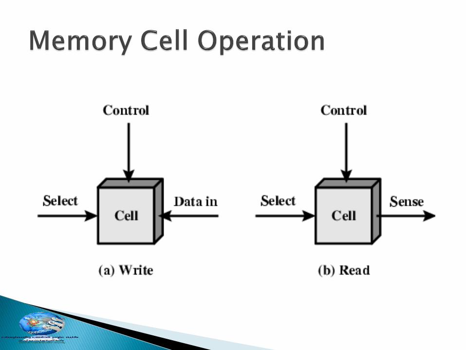
Bits stored as charge in capacitors
Charges leak
Need refreshing even when powered
Simpler construction
Smaller per bit
Less expensive
Need refresh circuits
Slower
Main memory
Essentially analogue ◦ Level of charge determines value
Bits stored as on/off switches
No charges to leak
No refreshing needed when powered
More complex construction
Larger per bit
More expensive
Does not need refresh circuits
Faster
Cache
Digital ◦ Uses flip-flops

Both volatile ◦ Power needed to preserve data
Dynamic cell ◦ Simpler to build, smaller ◦ More dense ◦ Less expensive ◦ Needs refresh ◦ Larger memory units
Static ◦ Faster ◦ Cache
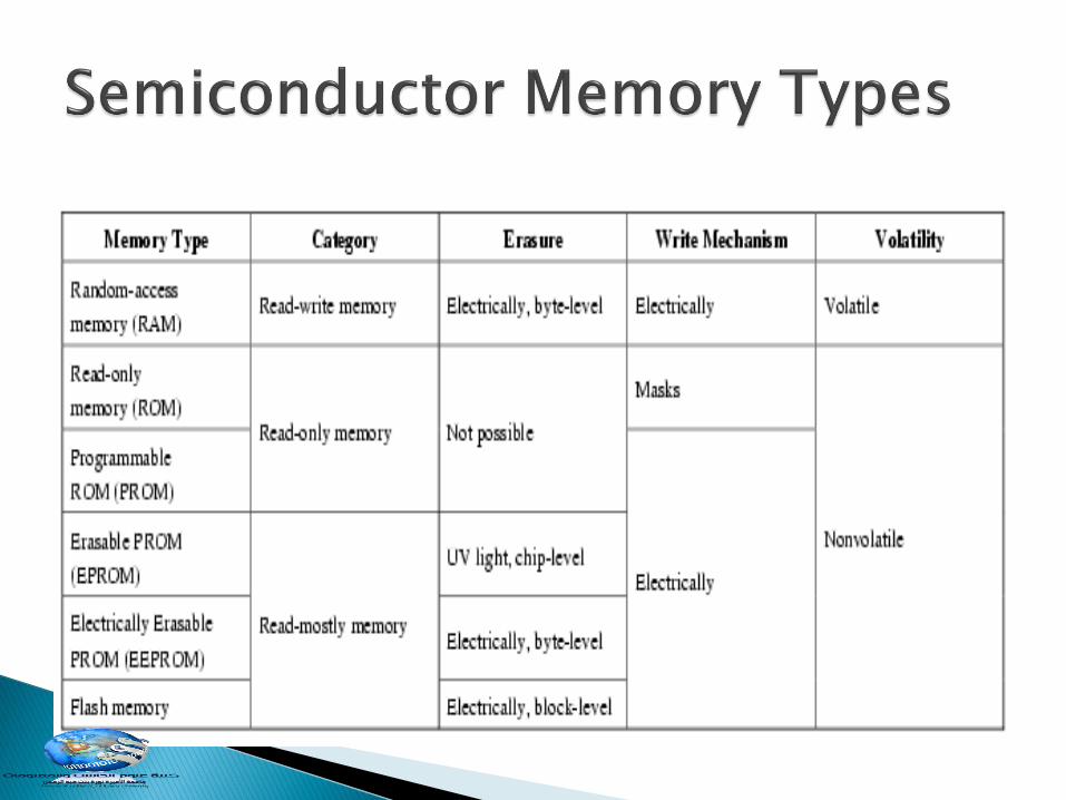
Permanent storage ◦ Nonvolatile
Microprogramming
Library subroutines
Systems programs (BIOS)
Function tables

Written during manufacture ◦ Very expensive for small runs
Programmable (once) ◦ PROM ◦ Needs special equipment to program
Read “mostly” ◦ Erasable Programmable (EPROM) Erased by UV
◦ Electrically Erasable (EEPROM) Takes much longer to write than read
◦ Flash memory Erase whole memory electrically
Hard Failure ◦ Permanent defect
Soft Error ◦ Random, non-destructive
◦ No permanent damage to memory
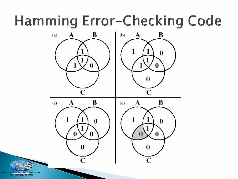
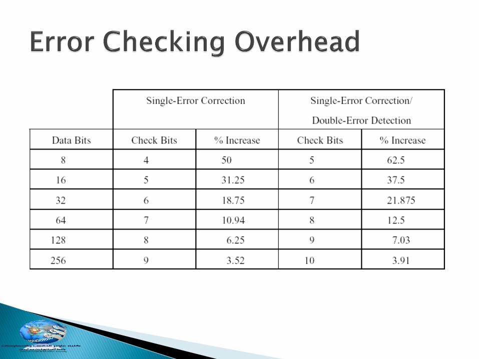
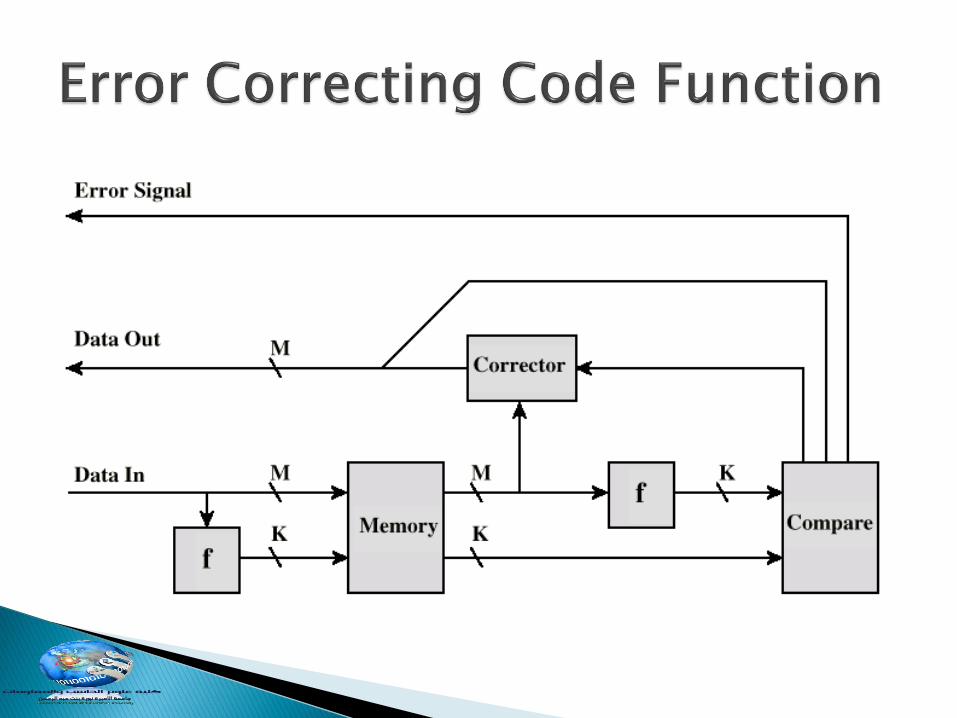
Detected using Hamming error correcting code
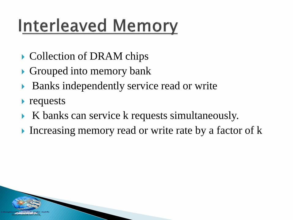
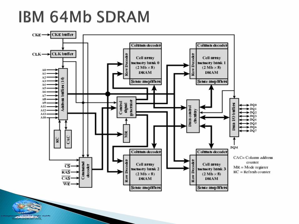
Collection of DRAM chips
Grouped into memory bank
Banks independently service read or write
requests
K banks can service k requests simultaneously.
Increasing memory read or write rate by a factor of k
Basic DRAM same since first RAM chips
Enhanced DRAM ◦ Contains small SRAM as well
◦ SRAM holds last line read (c.f. Cache!)
Cache DRAM ◦ Larger SRAM component
◦ Use as cache or serial buffer
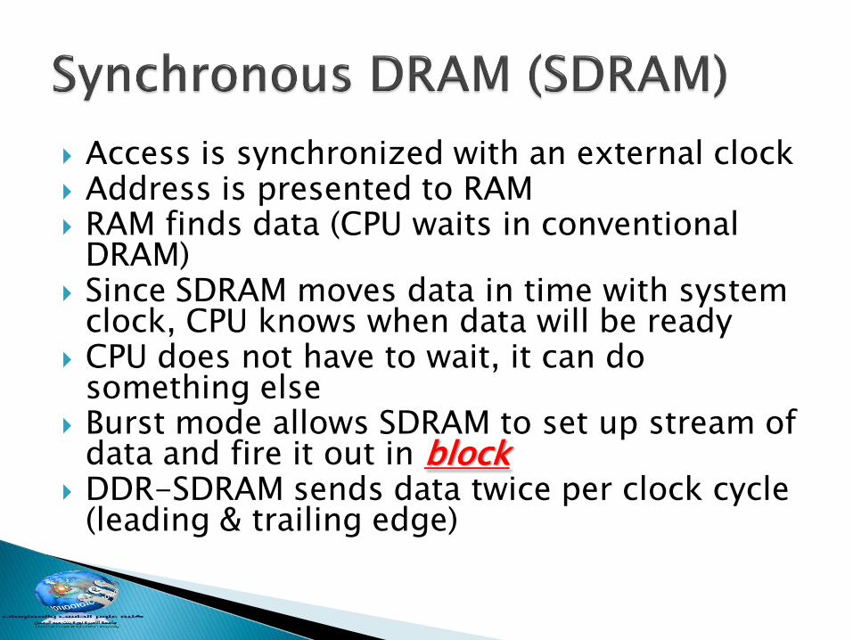
Access is synchronized with an external clock Address is presented to RAM RAM finds data (CPU waits in conventional
DRAM) Since SDRAM moves data in time with system
clock, CPU knows when data will be ready CPU does not have to wait, it can do
something else Burst mode allows SDRAM to set up stream of
data and fire it out in block DDR-SDRAM sends data twice per clock cycle
(leading & trailing edge)

Adopted by Intel for Pentium & Itanium processors
It has become the main competitor to SDRAM
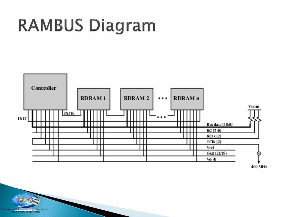
It has a vertical packages with all pins on one side
Data exchange over 28 wires < cm long
Bus addresses up to 320 RDRAM chips and rated at
1.6Gbps
It delivers address and control information using asynchronous block protocol
After an initial 480ns access time. This produces the 1.6 GBps data rate.
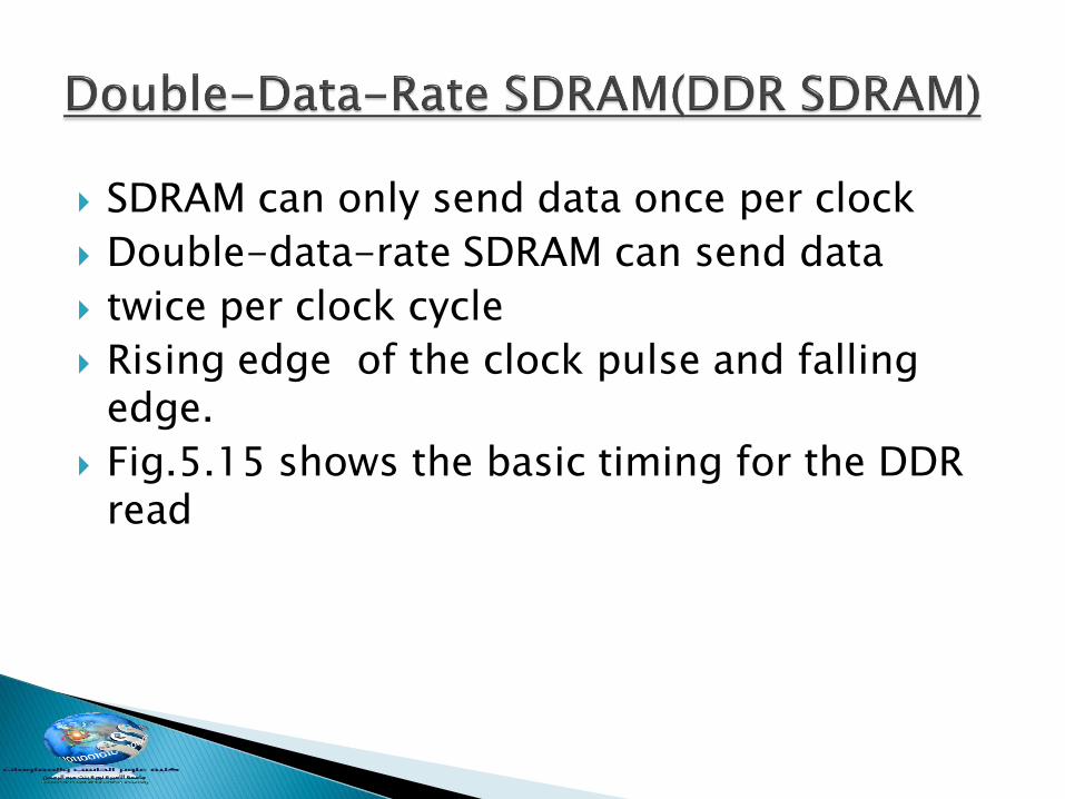
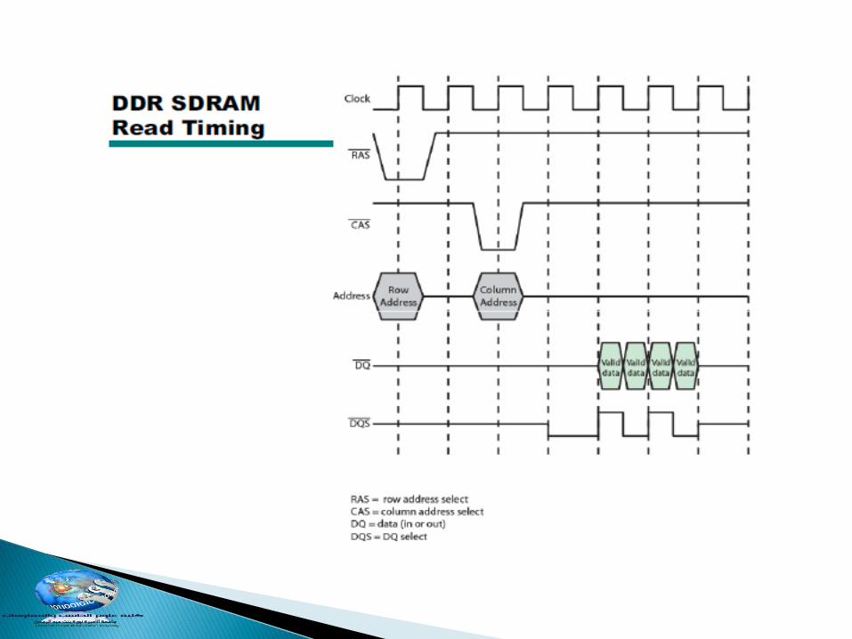
SDRAM can only send data once per clock
Double-data-rate SDRAM can send data
twice per clock cycle
Rising edge of the clock pulse and falling edge.
Fig.5.15 shows the basic timing for the DDR read
It developed by Mitsubishi. Integrates small SRAM cache (16 kb) onto generic
DRAM chip Used as true cache - 64-bit lines - Effective for ordinary random access To support serial access of block of data - refresh bit-mapped screen - CDRAM can prefetch data from DRAM into
SRAM buffer - Subsequent accesses solely to SRAM


![Banshee: Bandwidth-Efficient DRAM Caching Via Software ...Tagless DRAM Cache (TDC [10]) also uses address remap-ping, but enables frequent cache replacement via hardware-managed TLB](https://img.dokumen.tips/doc/110x75/5f5b2ff9c3e89664d66f964e/banshee-bandwidth-eficient-dram-caching-via-software-tagless-dram-cache-tdc.jpg)