Embed Size (px)
Citation preview
1 23
Journal of Electronic Materials ISSN 0361-5235 Journal of Elec MateriDOI 10.1007/s11664-013-2786-6
Interfacial Reactions Between Columnar orLayered Ni(P) Layers and Sn-Ag-Cu Solder
Y.J. Hu, Y.C. Hsu, C.T. Lu, T.S. Huang,C.Y. Chen, W.N. Chuang, C.Y. Hsiao,C.P. Lin & C.Y. Liu

1 23
Your article is protected by copyright and all
rights are held exclusively by TMS. This e-
offprint is for personal use only and shall not
be self-archived in electronic repositories. If
you wish to self-archive your article, please
use the accepted manuscript version for
posting on your own website. You may
further deposit the accepted manuscript
version in any repository, provided it is only
made publicly available 12 months after
official publication or later and provided
acknowledgement is given to the original
source of publication and a link is inserted
to the published article on Springer's
website. The link must be accompanied by
the following text: "The final publication is
available at link.springer.com”.
Interfacial Reactions Between Columnar or Layered Ni(P)Layers and Sn-Ag-Cu Solder
Y.J. HU,1,3 Y.C. HSU,1 C.T. LU,1 T.S. HUANG,1 C.Y. CHEN,1,4
W.N. CHUANG,1 C.Y. HSIAO,2 C.P. LIN,2 and C.Y. LIU1
1.—Department of Chemical Engineering and Materials Engineering, National Central Univer-sity, Jhongli 32001, Taiwan, ROC. 2.—Taiwan Uyemura Co., LTD., Taoyuan, Taiwan. 3.—e-mail:[email protected]. 4.—e-mail: [email protected]
Comparative study on the interfacial reactions between lead-free Sn-Ag-Cusolder and Ni(P) bond pads (with columnar or layered microstructure) hasbeen performed. The microstructure of the columnar Ni(P) is vertical, whilethe microstructure of the layered Ni(P) tends to be parallel to the solder/Ni(P)interface. The consumption rate of the columnar Ni(P, 7 at.%) layer is largerthan that of the layered Ni(P, 7 at.%). We believe that the faster Ni(P) con-sumption rate of the columnar Ni(P, 7 at.%) layer is due to the orientation ofthe grains. Spalling of the interfacial (Cu,Ni)6Sn5 compound can be seen at thereaction interfaces for the columnar Ni(P, 7 at.%) layer. On the contrary, nospalling can be seen for the case of the reacted layered Ni(P).
Key words: Electronic package, interfacial reaction, Pb-free solder, Ni(P)
INTRODUCTION
Electroless Ni(P) plating has been widely used asa diffusion barrier layer on Cu substrates for flip-chip and ball grid array solder bumps.1–4 The Ni(P)layer has been proved to have numerous advanta-ges, for example, a mature and low-cost platingprocess, and high resistance to corrosion. However,one of the major concerns regarding the use of Ni(P)bond pads is the solder-reaction-induced formationof the Ni3P compound between the Ni3Sn4 com-pound and the Ni(P) layer.3,4 Ni3P formation hasbeen reported to cause (1) serious voids inside theNi3P layer and a gap underneath the Ni3P layer,and (2) spalling of the Ni3Sn4 compound layer.These two phenomena degrade the reliability of thesolder joints.5,6
In the current Ni(P) electroless plating process,the Ni(P) usually has a layered crystalline struc-ture. This means that the grains of Ni(P) appear tohave an elongated shape. Owing to this layeredshape, the Ni(P) layer is quite brittle. Bending caneasily cause the Ni(P) layer to crack. Nowadays,flexible substrates are widely used in handheld
devices. The Ni(P) layer plated on such flexiblesubstrates needs to be more flexible and ductile.One approach to produce a ductile Ni(P) layer is tomanipulate the microstructure of the Ni(P) layer. Ina private communication from Taiwan UyemuraCorporation, their internal results show that a Ni(P)layer with columnar crystalline structure wouldhave improved ductility. In this study, firstly, weinvestigate the interfacial reactions between lead-free SAC305 solder and a Ni(P) bond pad withcolumnar microstructure. It is known that thephosphorous (P) in the electroless Ni(P) wouldgreatly influence the reliability of the solder joints.So, in this paper, we also study the effect of the Pcontent on the interfacial reaction with the samereflow processes.
EXPERIMENTAL PROCEDURES
Figure 1 illustrates the studied bump jointstructure. Sn-3Ag-0.5Cu (wt.%) solder bumps werereflowed on electroless Ni immersion gold bond padson the Cu pads of a FR4 printed circuit board. Thethickness of the Ni(P) layer was about 4.75 lm to5 lm, and the thickness of the immersion Au layerwas about 0.06 lm. The opening in the passivationlayer was about 500 lm. Two kinds of Ni(P) layer(Received May 2, 2013; accepted September 7, 2013)
Journal of ELECTRONIC MATERIALS
DOI: 10.1007/s11664-013-2786-6� 2013 TMS
Author's personal copy

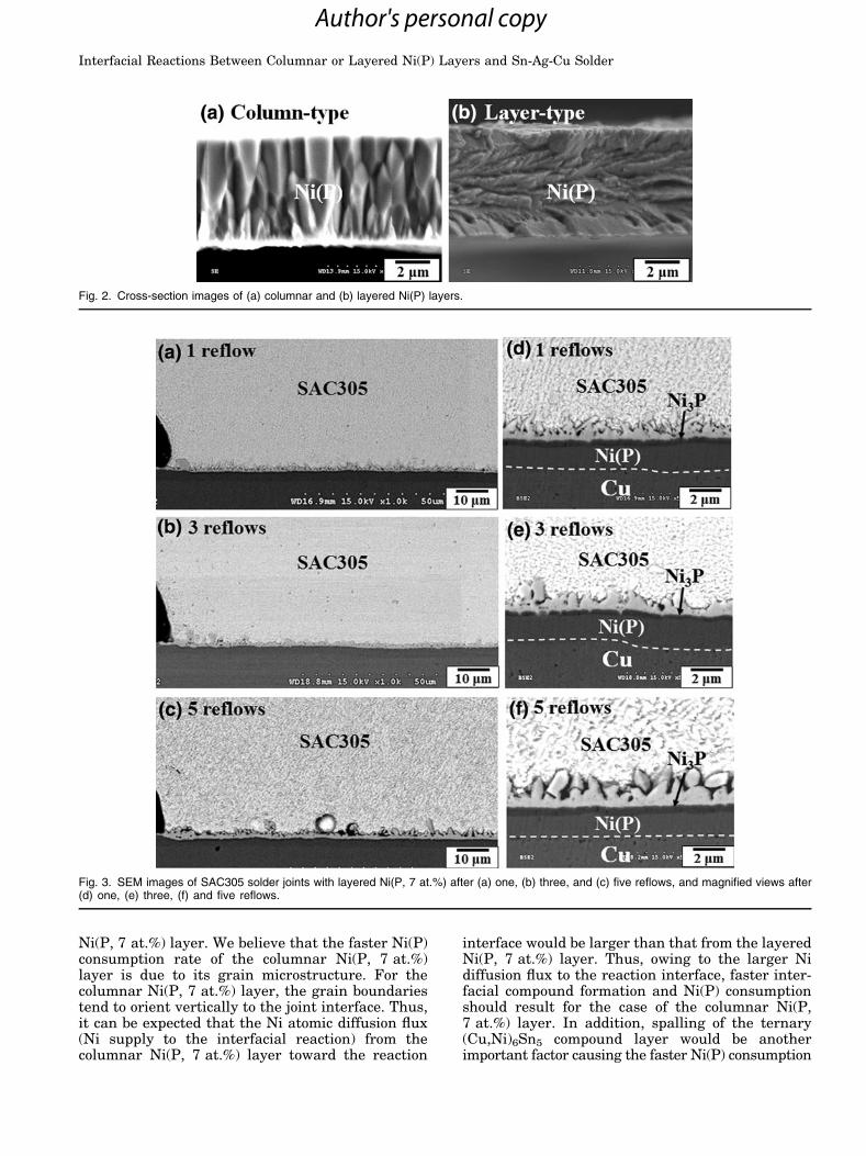
were prepared by electroless plating processes,having columnar and layered crystalline structure,respectively. Figure 2a and b show cleaved cross-sectional images of the columnar and layered Ni(P)layers, respectively. One can clearly see that thegrain microstructure of the columnar Ni(P) layertends to be vertical to the Ni(P) layer, whereas thegrain microstructure of the layered Ni(P) layertends to be parallel to the Ni(P) layer. The P contentin both Ni(P) layers was about 7 at.%.
Then, the prepared Au/Ni(P)/Cu bond pads werereflowed with 760-lm-diameter Sn-Ag-Cu solderballs. Note that the Au/Ni(P)/Cu bond pads wereprefluxed with a thin rosin mildly activated (RMA)-type flux. The reflow temperature was 250�C, andthe duration of each reflow was 60 s. Samples weresubjected to one, three, or five reflows. After a cer-tain number of reflows, the samples were removedfrom the hotplate and air-cooled at room tempera-ture. The reflowed samples were mounted withepoxy resin and polished with sandpaper and pol-ishing cloths. The fine-polished samples wereexamined by scanning electron microscopy (SEM).The compositions of the interfacial phases wereanalyzed by field-emission electron probe micro-analysis (FE-EPMA). The analyzer electron beamsize used to verify the compound phases was0.5 lm 9 0.5 lm.
The second part of this work studied the effect ofthe P content on the soldering reaction. By varyingthe electroless plating condition, the P content inthe Ni(P) layers can be increased to 10 at.% witha layered microstructure. All the reflow processeswere the same as the previous experimentalconditions.
RESULTS AND DISCUSSION
Interfacial Reaction of Layered and ColumnarNi(P) Layers
Figure 3a, b, and c show SEM cross-sectionalimages at the interfaces between layered Ni(P,7 at.%) and Sn-Ag-Cu solder after one, three, andfive reflows, respectively. The reactions between
Sn-rich Pb-free solders and Ni(P) bond pads havebeen studied by many researchers.7–10 Typically, itis known that the top Au finish layer quickly dis-solves into the molten solder. In this study, by usingFE-EPMA analysis, we also verified that the Aufinish layer on the Ni(P) metal bond pad dissolvedinto the molten SAC305 solder; no Au-containingcompound phases could be detected at the interfaceor inside the solder matrix. We believe that theentire Au layer on the Ni(P) layer quickly dissolvedinto the molten Sn-Ag-Cu solder, and no Au elementcould be detected in the interfacial compound pha-ses. Thus, the Au layer on the Ni(P) layer did notplay a role in the Sn-Ag-Cu/Ni(P) interfacial reac-tion.
As seen in Fig. 3, the interfacial intermetallic com-pound layer shows the common scallop-type morphol-ogy, being found to be the ternary (Cu,Ni)6Sn5
compound phase by FE-EPMA (electron-probe x-raymicroanalysis). The ternary (Cu,Ni)6Sn5 intermetalliccompound phase has been observed in many previousworks on the reactions between Cu-containing Sn-richsolders and Ni(P) metal bond pads.3–5,7,8,10–12 Also, alayer of the Ni3P compound phase can be seen under-neath the ternary (Cu,Ni)6Sn5 compound layer, asindicated by arrows in Fig. 3d–f. The formation of aNi3P layer has been proven to be caused by the mech-anism of ‘‘solder-reaction-assisted crystallization.’’11,12
As theNi3P layergrowswith thenumberof reflows, theP content in the Ni(P) layer would be enriched andpromote the growth of the Ni3P layer. Typically,workers agree that the growth of the interfacial(Cu,Ni)6Sn5 compound layer consumes Ni from theNi(P) layer and enhances the growth of the Ni3P layer.
Figure 4a, b, and c show cross-sectional images atthe interfaces between columnar Ni(P, 7 at.%) andSn-Ag-Cu solder after one, three, and five reflows,respectively. As for the reaction of the layered Ni(P)layer, the ternary (Cu,Ni)6Sn5 compound is alsoobserved at the interface. However, we found thatthe morphology of the interfacial (Cu,Ni)6Sn5 com-pound in the case of the columnar Ni(P, 7 at.%)layer has a facet-like appearance, which is closer tothe morphology of the Ni3Sn4 compound formed atthe Ni/Sn reaction interface. On the other hand, themorphology of the interfacial (Cu,Ni)6Sn5 compoundin the case of the layered Ni(P, 7 at.%) layer shows amore scallop shape, which is commonly observed inthe Cu6Sn5 compound at the Cu/Sn reaction inter-face.13,14 Thus, we believe that the interfacial(Cu,Ni)6Sn5 compound in the case of the columnarNi(P, 7 at.%) layer could contain more Ni contentthan the interfacial (Cu,Ni)6Sn5 compound in the caseof the layered Ni(P, 7 at.%) layer. This expectationalso agrees with the data presented in Table I show-ing that the columnar Ni(P, 7 at.%) layer containsmore Ni content than the layered Ni(P, 7 at.%) layer.
Figure 5a shows the consumed thickness of theNi(P) layer versus the number of reflows. It is foundthat the Ni(P) consumption rate of the columnarNi(P, 7 at.%) layer is larger than that of the layered
Fig. 1. Schematic of a solder joint with a Ni(P) layer.
Hu, Hsu, Lu, Huang, Chen, Chuang, Hsiao, Lin, and Liu
Author's personal copy
Ni(P, 7 at.%) layer. We believe that the faster Ni(P)consumption rate of the columnar Ni(P, 7 at.%)layer is due to its grain microstructure. For thecolumnar Ni(P, 7 at.%) layer, the grain boundariestend to orient vertically to the joint interface. Thus,it can be expected that the Ni atomic diffusion flux(Ni supply to the interfacial reaction) from thecolumnar Ni(P, 7 at.%) layer toward the reaction
interface would be larger than that from the layeredNi(P, 7 at.%) layer. Thus, owing to the larger Nidiffusion flux to the reaction interface, faster inter-facial compound formation and Ni(P) consumptionshould result for the case of the columnar Ni(P,7 at.%) layer. In addition, spalling of the ternary(Cu,Ni)6Sn5 compound layer would be anotherimportant factor causing the faster Ni(P) consumption
Fig. 2. Cross-section images of (a) columnar and (b) layered Ni(P) layers.
Fig. 3. SEM images of SAC305 solder joints with layered Ni(P, 7 at.%) after (a) one, (b) three, and (c) five reflows, and magnified views after(d) one, (e) three, (f) and five reflows.
Interfacial Reactions Between Columnar or Layered Ni(P) Layers and Sn-Ag-Cu Solder
Author's personal copy

for the case of the columnar Ni(P, 7 at.%) layer.As shown in Fig. 4, spalling of the interfacial(Cu,Ni)6Sn5 compound can be seen at the Sn-Ag-Cu/Ni(P, 7 at.%) reaction interfaces. After one reflow, asmall amount of compound grains can be seen spalledabove the reaction interface. After three reflows, twokinds of spalled-off compound grains are observed.Round-shaped compound grains are found spalledaway from the reaction interface, whereas smallplate-like compound grains are spalled off at thereaction interface. After five reflows, more plate-likecompound grains are spalled off at the reaction
interface. As the interfacial (Cu,Ni)6Sn5 compoundspalled away from the Sn-Ag-Cu/Ni(P) reactioninterface, the molten Sn-Ag-Cu solder would likely
Fig. 4. SEM images of SAC305 solder joints with columnar Ni(P, 7 at.%) after (a) one, (b) three, and (c) five reflows, and magnified views after(d) one, (e) three, and (f) five reflows.
Table I. EPMA analysis of Ni content at middle andouter region for different substrates
Middle Region(Ni wt.%)
Outer Region(Ni wt.%)
7% P layered 89.063 88.5457% P columnar 90.667 89.20110% P layered 84.037 82.15211% P layered 85.942 84.539
Fig. 5. Thickness of Ni(P) consumption versus number of reflows at250�C.
Hu, Hsu, Lu, Huang, Chen, Chuang, Hsiao, Lin, and Liu
Author's personal copy

react with the Ni(P) layer directly. Consequently, theNi(P) consumption would be enhanced in the case ofthe columnar Ni(P, 7 at.%) layer. It is well acceptedthat the left-over P content owing to Ni(P) consump-tion is the key to the formation of the Ni3P layer.Thus, the degree of Ni consumption would be pro-portional to the formation of the Ni3P layer. In thecurrent results, we observe that the Ni(P) consump-tion in the columnar Ni(P) case is much greater thanin the layered Ni(P) case after five reflows. However,the Ni3P thickness in the columnar Ni(P) case is notvery different from that in the layered Ni(P) case. Wetend to believe that part of the Ni3P layer in thecolumnar Ni(P) case reacted with the solder to formeda Sn-Ni-P layer, which is why we do not observe moreNi3P forming in the case of the columnar Ni(P) layer.
Another important finding is that a continuousNi–Sn-P layer is observed between the interfacial(Cu,Ni)6Sn5 compound layer and the Ni3P layer inthe case of the columnar Ni(P, 7 at.%) layer, asindicated by arrows in Fig. 4e, f. Such a continuousNi-Sn-P layer has been observed by manyresearchers.15–17 Also, we note that, in the case ofthe layered Ni(P, 7 at.%) layer, we can hardlyobserve the Ni-Sn-P layer at the reaction interface.We believe that spalling of the interfacial (Cu,Ni)6Sn5 compound at the reaction is the key to theformation of this Ni-Sn-P layer, because it causes a
direct reaction between the molten Sn-Ag-Cu solderand the Ni(P) layer. There are several reasons forthe spalling of the interfacial (Cu,Ni)6Sn5 compoundon the Ni-Sn-P layer. Firstly, the interfacial energybetween the interfacial (Cu,Ni)6Sn5 compound andthe Ni-Sn-P layer could be very high, thus theinterfacial (Cu,Ni)6Sn5 compound tends to spall offthe Ni-Sn-P layer to reduce the total energy ofthe system. As seen in Fig. 4f, after five reflows, theNi-Sn-P layer at the interface with the spalled-off(Cu,Ni)6Sn5 compound is much thicker than that atthe interface without spalling. Another possiblereason for the spalling of the interfacial (Cu,Ni)6Sn5
compound on the Ni-Sn-P layer could be the higherNi diffusion into the interfacial (Cu,Ni)6Sn5 com-pound. As mentioned above, the greatest differencebetween the layered and columnar Ni(P, 7 at.%)layers lies in the grain microstructure and the grainboundary orientation. For the columnar Ni(P,7 at.%) layer, the grain boundaries tend to be ver-tical to the joint interface. Thus, it can be expectedthat Ni in the columnar Ni(P, 7 at.%) layer couldhave a greater tendency to diffuse to the reactioninterface and form an interfacial compound. Such alarge amount of Ni incorporated into the interfacialcompounds could cause a change in the morphology(to become the more facet-like Ni3Sn4 compound).As a result, a change in the morphology could be
Fig. 6. SEM cross-sectional images at interfaces between layered Ni(10 at.% P) and Sn-Ag-Cu solder after (a, d) one, (b, e) three, and (c, f) fivereflows.
Interfacial Reactions Between Columnar or Layered Ni(P) Layers and Sn-Ag-Cu Solder
Author's personal copy
another possible cause for the spalling of the inter-facial (Cu, Ni)6Sn5 compound on the Ni-Sn-P layer.
High-P Layered Ni(P, 10 at.%) Reactedwith Sn-Ag-Cu Solder
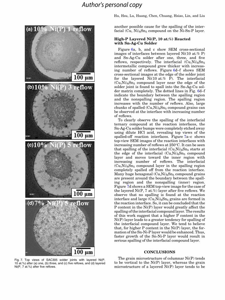
Figure 6a, b, and c show SEM cross-sectionalimages of interfaces between layered Ni(10 at.% P)and Sn-Ag-Cu solder after one, three, and fivereflows, respectively. The interfacial (Cu,Ni)6Sn5
intermetallic compound grew thicker with increas-ing number of reflows. Figure 6d–f shows SEMcross-sectional images at the edge of the solder jointfor the layered Ni(10 at.% P). The interfacial(Cu,Ni)6Sn5 compound layer near the edge of thesolder joint is found to spall into the Sn-Ag-Cu sol-der matrix completely. The dotted lines in Fig. 6d–findicate the boundary between the spalling regionand the nonspalling region. The spalling regionincreases with the number of reflows. Also, largechunks of spalled (Cu,Ni)6Sn5 compound grains canbe observed at the interface with increasing numberof reflows.
To clearly observe the spalling of the interfacialternary compound at the reaction interfaces, theSn-Ag-Cu solder bumps were completely etched awayusing dilute HCl acid, revealing top views of thespalled-off reaction interfaces. Figure 7a–c showstop-view SEM images of the reaction interfaces withincreasing number of reflows at 250�C. It can be seenthat spalling of the interfacial (Cu,Ni)6Sn5 starts atthe edge of the interfacial (Cu,Ni)6Sn5 compoundlayer and moves toward the inner region withincreasing number of reflows. The interfacial(Cu,Ni)6Sn5 compound layer in the spalling regioncompletely spalled off from the reaction interface.Many huge hexagonal (Cu,Ni)6Sn5 compound grainsare present around the boundary between the spall-ing region and the nonspalling (inner) region.Figure 7d shows a SEM top-view image for the case ofthe layered Ni(P, 7 at.%) layer after five reflows. Weobserve that no spalling is found at the reactioninterface and large (Cu,Ni)6Sn5 grains are formed inthe reaction interface. So, it can be concluded that theP content in the Ni(P) layer would greatly affect thespalling of the interfacial compound layer. The resultsof this work suggest that a higher P content in theNi(P) layer leads to a greater tendency for spalling ofthe interfacial compound layer. We tend to believethat, for higher P content in the Ni(P) layer, the for-mation of the Sn-Ni-P layer would be enhanced. Thus,faster growth of the Sn-Ni-P layer would result inserious spalling of the interfacial compound layer.
CONCLUSIONS
The grain microstructure of columnar Ni(P) tendsto be vertical to the Ni(P) layer, whereas the grainmicrostructure of a layered Ni(P) layer tends to be
Fig. 7. Top views of SAC305 solder joints with layered Ni(P,10 at.%) after (a) one, (b) three, and (c) five reflows, and (d) layeredNi(P, 7 at.%) after five reflows.
Hu, Hsu, Lu, Huang, Chen, Chuang, Hsiao, Lin, and Liu
Author's personal copy
parallel to the Ni(P) layer. The present results showthat the Ni(P) consumption rate of the columnarNi(P, 7 at.%) layer is larger than that of the layeredNi(P, 7 at.%) layer. We believe that the faster Ni(P)consumption rate of the columnar Ni(P, 7 at.%)layer is due to the orientation of the grain structure.Spalling of the interfacial (Cu,Ni)6Sn5 compoundcan be seen at the reaction interfaces of the colum-nar Ni(P, 7 at.%) layer. On the contrary, no spallingcan be seen for the case of the layered Ni(P) layer.Spalling of the ternary (Cu,Ni)6Sn5 compound layeris an important factor causing the faster Ni(P)consumption rate for the case of the columnar Ni(P,7 at.%) layer.
In addition, we investigated the effect of the Pcontent on the interfacial reaction with Sn-Ag-Cusolder. The results of this work show that higher Pcontent in the Ni(P) layer leads to a greater ten-dency for spalling of the interfacial compound layer.We tend to believe that, for higher P content, theformation of the Sn-Ni-P layer would be enhanced.Thus, the faster growth of the Sn-Ni-P layer wouldresult in serious spalling of the interfacial com-pound layer.
ACKNOWLEDGEMENTS
This study was supported by Taiwan UyemuraCo., Ltd. and in part by the National Central Uni-versity’s Plan to Develop First-class Universities,top-level Research Centers Grants 100G903-2, and
National Science Council Grant Projects NSC 98-2221-E-008-027-MY3 and NSC 100-3113-E-008-00.
REFERENCES
1. J.W. Yoon, C.B. Lee, and S.B. Jung, J. Electron. Mater. 32,1195 (2003).
2. J.W. Yoon, C.B. Lee, and S.B. Jung, Mater. Trans. 43, 1821(2002).
3. M. He, Z. Chen, and G.J. Qi, Acta Mater. 52, 2047 (2004).4. S.J. Wang and C.Y. Liu, Scr. Mater. 49, 813 (2003).5. J.W. Ronnie Teo and Y.F. Sun, Acta Mater. 56, 242 (2008).6. W.M. Chen, S.C. Yang, M.H. Tsai, and C.R. Kao, Scr. Mater.
63, 47 (2010).7. B.K. Kim, S.J. Lee, J.Y. Kim, K.Y. JI, Y.J. Yoon, M.Y. Kim,
S.H. Park, and J.S. Yoo, J. Electron. Mater. 37, 4 (2008).8. K. Zeng and K.N. Tu, Mater. Sci. Eng. R. 38, 55 (2002).9. M.O. Alam, Y.C. Chan, and K.N. Tu, J. Appl. Phys. 94, 6
(2003).10. Y. Jeon and K. Paik, Proceedings of the 51st Electronic
Components and Technology Conference (New York, NY:IEEE, 2001), p. 1326.
11. K.C. Hung and Y.C. Chan, J. Mater. Sci. Lett. 19, 1755(2000).
12. J.W. Jang, P.G. Kim, and K.N. Tu, J. Appl. Phys. 85, 12(1999).
13. K.S. Kim, S.H. Huh, and K. Suganuma, J. Alloy. Compd.352, 226–236 (2003).
14. J.W. Yoon, B.I. Noh, B.K. Kim, C.C. Shur, and S.B. Jung,J. Alloy. Compd. 486, 142–147 (2009).
15. Y.C. Sohn, J. Yu, S.K. Kang, D.Y. Shih, and T.Y. Lee,J. Mater. Res. 19, 8 (2004).
16. Y.C. Lin, K.J. Wang, and J.G. Duh, J. Electron. Mater. 39, 3(2010).
17. T. Laurila, V. Vuorinen, and J.K. Kivilahti, Mater. Sci. Eng.R. 49, 1 (2005).
Interfacial Reactions Between Columnar or Layered Ni(P) Layers and Sn-Ag-Cu Solder
Author's personal copy


![1 Interfacial Rheology System. 2 Background of Interfacial Rheology Interfacial Shear Stress Interfacial Shear Viscosity = [ ]](https://img.dokumen.tips/doc/110x75/56649d1f5503460f949f3d29/1-interfacial-rheology-system-2-background-of-interfacial-rheology-interfacial.jpg)