Embed Size (px)
Citation preview

Interface Manual
USB HID – I2C
(Rev 1.04)
Luxemburger Str. 31 D – 13353 Berlin
Phone: +49 – (0)30 – 61 74 12 48
Fax: +49 – (0)30 – 61 74 12 47 www.coptonix.com

Rev1.04 October 2011
2
1. OPENING A DEVICE ...................................................................................................................................... 3
1.1 HIDD_GETHIDGUID ..................................................................................................................................... 3 1.2 SETUPDIGETCLASSDEVS.............................................................................................................................. 3 1.3 SETUPDIENUMDEVICEINTERFACE ................................................................................................................ 3 1.4 SETUPDIGETDEVICEINTERFACEDETAIL ....................................................................................................... 4 1.5 CREATEFILE .................................................................................................................................................. 4
2. REPORTS (IN & OUT).................................................................................................................................... 6
3. COMMANDS .................................................................................................................................................... 7
3.1 SET I2C MODE (0X00)................................................................................................................................ 7 3.2 I2C WRITE (0X01)....................................................................................................................................... 7 3.3 I2C READ (0X02)......................................................................................................................................... 8 3.4 I2C WRITE READ (0X08) ........................................................................................................................... 9 3.5 CHECK SLAVE ADDRESS (0X07) .......................................................................................................... 10 3.6 SCAN I2C BUS (0X05) .............................................................................................................................. 10 3.7 SET I2C FREQUENCY (0X03).................................................................................................................. 11 3.8 GET I2C FREQUENCY (0X04) ................................................................................................................. 12 3.9 SET IRQ MODE (0X06) ............................................................................................................................. 13 3.10 IRQ EVENT (0X09, 0XF6) ....................................................................................................................... 13 3.11 SET SLAVE ADDRESS (0X83)............................................................................................................... 14 3.12 WRITE SLAVE BUFFER (0X81) ............................................................................................................ 15 3.13 SLAVE DATA (0X82, 0X7E) ................................................................................................................... 15 3.14 EXECUTE COMMAND DENIED (0XFE).............................................................................................. 16 3.15 UNKNOWN COMMAND (0XFF)........................................................................................................... 16 3.16 MEM WR 8BIT (0X20) ............................................................................................................................ 17 3.17 MEM WR 16BIT (0X21) .......................................................................................................................... 18 3.18 MEM WR 32BIT (0X22) .......................................................................................................................... 19 3.19 MEM WR BLOCK (0X23) ....................................................................................................................... 20 3.20 MEM RD 8BIT (0X24) ............................................................................................................................. 21 3.21 MEM RD 16BIT (0X25) ........................................................................................................................... 21 3.22 MEM RD 32BIT (0X26) ........................................................................................................................... 22 3.23 MEM RD BLOCK (0X27) ........................................................................................................................ 23 3.24 SAVE SETTINGS (0X28) ........................................................................................................................ 23 3.25 RESET SETTINGS (0X29)....................................................................................................................... 24
Rev1.04 October 2011
3
1. Opening a device The USB I2C Converter MS uses the HID class (Human Interface Device). The HID class is a standard device classification for the USB. The most of the operating systems (e.g. Windows, Mac, Linux) offers a HID class driver, so that there is no need for additional drivers to communicate with the converter. Developers should only know how to use the native API functions offered by the operating system. For communication an application must be first able to open the device. The process of opening a device is done as follow:
1.1 HidD_GetHidGuid Call the function HidD_GetHidGuid (hid.dll) to obtain the Windows GUID (globally unique identifier) for HID devices.
VOID HidD_GetHidGuid(OUT LPGUID HidGuid); HidD_GetHidGuid(&HidGuid);
1.2 SetupDiGetClassDevs Call the function SetupDiGetClassDevs (setupapi.dll) to get an array of structure that contain information about all attached HIDs. This function needs the previously obtained HID GUID to specify that the list should contain only HID devices.
HDEVINFO SetupDiGetClassDevs(
IN LPGUID ClassGuid, OPTIONAL IN PCTSTR Enumerator, OPTIONAL IN HWND hwndParent, OPTIONAL IN DWORD Flags);
hDevInfo = SetupDiGetClassDevsA(
@HidGuid, NULL, NULL, DIGCF_PRESENT | DIGCF_DEVICEINTERFACE);
DIGCF_PRESENT: Return only devices that are currently present in a system. DIGCF_DEVICEINTERFACE: Return devices that support device interface for the
specified device interface class.
1.3 SetupDiEnumDeviceInterface Call the function SetupDiEnumDeviceInterface (setupapi.dll) to get information about a device in the list. Use a loop to step through each index of device information until the device with the correct VID (0x19D1) and PID (0x00A0) is found. If the function returns FALSE, then the end of the list is reached.
BOOLEAN SetupDiEnumDeviceInterface(
IN HDEVINFO DeviceInfoSet, IN PSP_DEVINFO_DATA DeviceInfoData, OPTIONAL IN LPGUID InterfaceClassGuid, IN DWORD MemberIndex, OUT PSP_DEVICE_INTERFACE_DATA DeviceInterfaceData);

Rev1.04 October 2011
4
devInfoData.cbSize = sizeof(devInfoData); Result = SetupDiEnumDeviceInterfaces(hDevInfo,
0, &HidGuid, MemberIndex,
&devInfoData);
1.4 SetupDiGetDeviceInterfaceDetail Call the function SetupDiGetDeviceInterfaceDetail (setupapi.dll) to get the device path of the device indexed in the previous step.
BOOLEAN SetupDiGetDeviceInterfaceDetail(
IN HDEVINFO DeviceInfoSet, IN PSP_DEVICE_INTERFACE_DATA DeviceInterfaceData, OUT PSP_DEVICE_INTERFACE_DETAIL_DATA DeviceInterfaceDetailData, OPTIONAL IN DWORD DeviceInterfaceDetailDataSize, OUT PDWORD RequiredSize, OPTIONAL OUT PSP_DEVINFO_DATA DeviceInfoData, OPTIONAL);
Result = SetupDiGetDeviceInterfaceDetail(
hdevInfo, &devInfoData, detailData,
Length, &Required, NULL);
The structure SP_DEVICE_INTERFACE_DETAIL_DATA is defined as follow:
typedef struct _SP_DEVICE_INTERFACE_DETAIL_DATA { DWORD cbSize; TCHAR DevicePath[ANYSIZE_ARRAY];
} SP_DEVICE_INTERFACE_DETAIL_DATA, *PSP_DEVICE_INTERFACE_DETAIL_DATA;
detailData->DevicePath is the device path we need to open the device.
1.5 CreateFile Call the function CreateFile using the device path to open a device. The return value of this function is the handle of the device.
HANDLE CreateFile(
LPCTSTR lpFileName, DWORD dwDesiredAccess, DWORD dwSharedMode, LPSECURITY_ATTRIBUTES lpSecurityAttributes, DWORD dwCreationDisposition, DWORD dwFlagsAndAttributes,
HANDLE hTemplateFile);

Rev1.04 October 2011
5
DevHandle = CreateFile( detailData->DevicePath, GENERIC_READ | GENERIC_WRITE, FILE_SHARE_READ | FILE_SHARE_WRITE, (LPSECURITY_ATTRIBUTES)NULL, OPEN_EXISTING, 0, NULL);
Reading and writing reports are done with the functions ReadFile and WriteFile. These functions use the handle returned by the function CreateFile.

Rev1.04 October 2011
6
2. Reports (IN & OUT) Reports (IN and OUT) contain always 65 bytes including the report ID.
Offset Report ID
State Length
Low High Data
0 Data
1 … Data
59
0 0/1 1..60 0..2047 0.255 0..255 0..255 0..255
Field Size (Byte) Value Description Report-ID 1 0 Should always set to zero (0)
0 Indicates if one or more reports will follow State 1 1 Indicates the last report
Length 1 1..60 Is the number of valid data bytes in the report (Data 0..59)
Offset 2 0..2047 I2C buffer offset Data 0 .. 59 1 0..255 Each report may contain up to 60 bytes, but
at least one byte. Example (I2C write transaction): 135 Bytes (d1,d2,…,d135) should be written to slave 64 (0x40). Command: 1 Slave: 64 Length: 135 This means, we have to send 139 (135 + 4) bytes. The data is sent in 60 bytes chunks. In total we have to send 3 reports. First and second report each contains 60 data bytes (State = 0), and the third (last) report contains only 19 valid data bytes (State = 1). 1. Report (5 bytes header + 60 bytes data):
Offset Low High
Data 0
Data 1
Data 2
Data 3
Data 4..59
Length
Report ID
State Length
0 0 CMD Slave Low High
d1..d56
0 0 60 0 1 64 135 0 0..255 2. Report:
Offset
Low High Data 0..59
Report ID
State Length
60 0 d57..d116
0 0 60 60 0..255 3. Report:
Offset Low High
Data 0..18
Data 19..59
Report ID
State Length
120 0 d117..d135 no more data 0 1 19 120 0..255 X (do not care)
0 1 2 3 4..59 60..119 120..138 1.Report (4 bytes I2C header + 56 bytes) 2.Report (60 bytes) 3.Report (19 bytes)
CMD Slave Length Data Data Data 1 64 135 0 d1..d56 d57..d116 d117..d135
Converter’s I2C Buffer
Offset: 0 Offset: 60 Offset: 120

Rev1.04 October 2011
7
3. Commands
3.1 SET I2C MODE (0x00) This command selects one of two operating modes: MASTER_MODE or SLAVE_MODE. OUT Report:
Offset Data Report ID
State Length
Low High 0 1 2 3..59 0 1 3 0 ucCMD ucMode ucSlvAddr X
IN Report:
Offset Data Report ID
State Length
Low High 0 1 2 3..59 0 1 3 0 ucCMD ucMode ucSlvAddr X
Field Size (Byte) Value Description
ucCMD 1 0x00 SET I2C MODE command 0x00 Reads current mode 0x01 MASTER_MODE
ucMode 1
0x02 SLAVE_MODE ucSlvAddr 1 0x01..0xFF Is the slave address of the converter (valid
only in SLAVE_MODE). If the LSB is 1, then the General Call is active.
X do not care
3.2 I2C WRITE (0x01) This command initiates I2C WRITE transaction. OUT Report:
Offset Data Report ID
State Length
Lo Hi 0 1 2..3 4..59
wLength 0 0/1 4..60 0..2050 ucCMD ucSlvAddr Lo Hi
data
If more than 56 bytes should be written, then more OUT Reports (each 60 + 5 bytes) may be sent. State = 1 indicates last OUT Report. IN Report:
Offset Data Report ID
State Length
Lo Hi 0 1 2..3 4..5 6..59
wLength wStatus 0 1 6 0 ucCMD ucSlvAddr Lo Hi Lo Hi
X
Field Size (Byte) Value Description
ucCMD 1 0x01 I2C WRITE command ucSlvAddr 1 0x02..0xFE Slave address wLength 2 1..2047 Number of bytes to write to slave address
“ucSlvAddr”. data 1..2047 0x00..0xFF Data to write to slave address “ucSlvAddr”.
Lo: 0x00..0x11 wStatus 2 Hi: 0x00..0x11
X do not care
Rev1.04 October 2011
8
3.3 I2C READ (0x02) This command initiates I2C READ transactions. OUT Report:
Offset Data Report ID
State Length
Lo Hi 0 1 2..3 4..59 wLength 0 0 4 0 ucCMD ucSlvAddr Lo Hi
X
IN Report:
Offset Data Report ID
State Length
Lo HI 0 1 2..3 4..5 6..59 wLength wStatus 0 0/1 6..60 0..2052 ucCMD ucSlvAddr Lo Hi Lo Hi
data
If more than 54 bytes were read, then more IN Reports (each 60 + 5 bytes) may be received. State = 1 indicates last IN Report.
Field Size (Byte) Value Description
ucCMD 1 0x02 I2C READ command ucSlvAddr 1 0x02..0xFE Slave address wLength 2 1..2047 Number of bytes to read from slave address
“ucSlvAddr”. data 1..2047 0x00..0xFF Data read from slave address “ucSlvAddr”.
Lo: 0x00..0x11 wStatus 2 Hi: 0x00..0x11
X do not care
Rev1.04 October 2011
9
3.4 I2C WRITE READ (0x08) This command initiates I2C WRITE transaction, then a REPEATED START and at last a READ transaction. OUT Report:
Offset Data Report ID
State Length
Lo Hi 0 1 2..3 4..5 6..59
wwrLength wrdLength 0 0/1 6..60 0..2052 ucCMD ucSlvAddr Lo Hi Lo Hi
wrdata
If more than 54 bytes should be written, then more OUT Reports (each 60 + 5 bytes) may be sent. State = 1 indicates last OUT Report. IN Report:
Offset Data Report ID
State Length
Lo Hi 0 1 2..3 4..5 6..59
wrdLength wStatus 0 0/1 6..60 0..2052 ucCMD ucSlvAddr Lo Hi Lo Hi
rddata
If more than 54 bytes were read, then more IN Reports (each 60 + 5 bytes) may be received. State = 1 indicates last IN Report.
Field Size (Byte) Value Description
ucCMD 1 0x08 I2C WRITE READ command ucSlvAddr 1 0x02..0xFE Slave address wwrLength 2 1..2047 Number of bytes to write to slave address
“ucSlvAddr”. wrdLength 2 1..2047 Number of bytes to read from slave address
“ucSlvAddr”. wrdata 1..2047 0x00..0xFF Data to write to slave address “ucSlvAddr”. rddata 1..2047 0x00..0xFF Data read from slave address “ucSlvAddr”.
Lo: 0x00..0x11 wStatus 2 Hi: 0x00..0x11
X do not care
Rev1.04 October 2011
10
3.5 CHECK SLAVE ADDRESS (0x07) This command checks if the slave address ucSlvAddr is connected to the I2C bus. OUT Report:
Offset Data Report ID
State Length
Low High 0 1 2..59 0 1 2 0 ucCMD ucSlvAddr X
IN Report:
Offset Data Report ID
State Length
Low High 0 1 2 3..59 0 1 3 0 ucCMD ucSlvAddr ucConnected X
Field Size (Byte) Value Description
ucCMD 1 0x07 Check slave address command ucSlvAddr 1 0x02..0xFE The slave address to be checked.
0x00 Device is not connected to the I2C bus. ucConnected 1 0x01 Device is connected to the I2C bus.
X do not care
3.6 SCAN I2C BUS (0x05) This command scans I2C devices currently connected to the I2C bus. OUT Report:
Offset Data Report ID
State Length
Low High 0 1..59 0 1 1 0 ucCMD X
IN Report:
Offset Data Report ID
State Length
Low High 0 1 2..59 0 0/1 2..60 0..120 ucCMD ucLength Devices
If more than 58 devices were detected, then more IN Reports (each 60 + 5 bytes) would be sent by the converter. State = 1 indicates last IN Report.
Field Size (Byte) Value Description
ucCMD 1 0x05 SCAN I2C BUS command ucLength 1 0x00..0x7F Number of devices detected. Devices 0..127 0x02..0xFE List of I2C devices were detected. X do not care
Rev1.04 October 2011
11
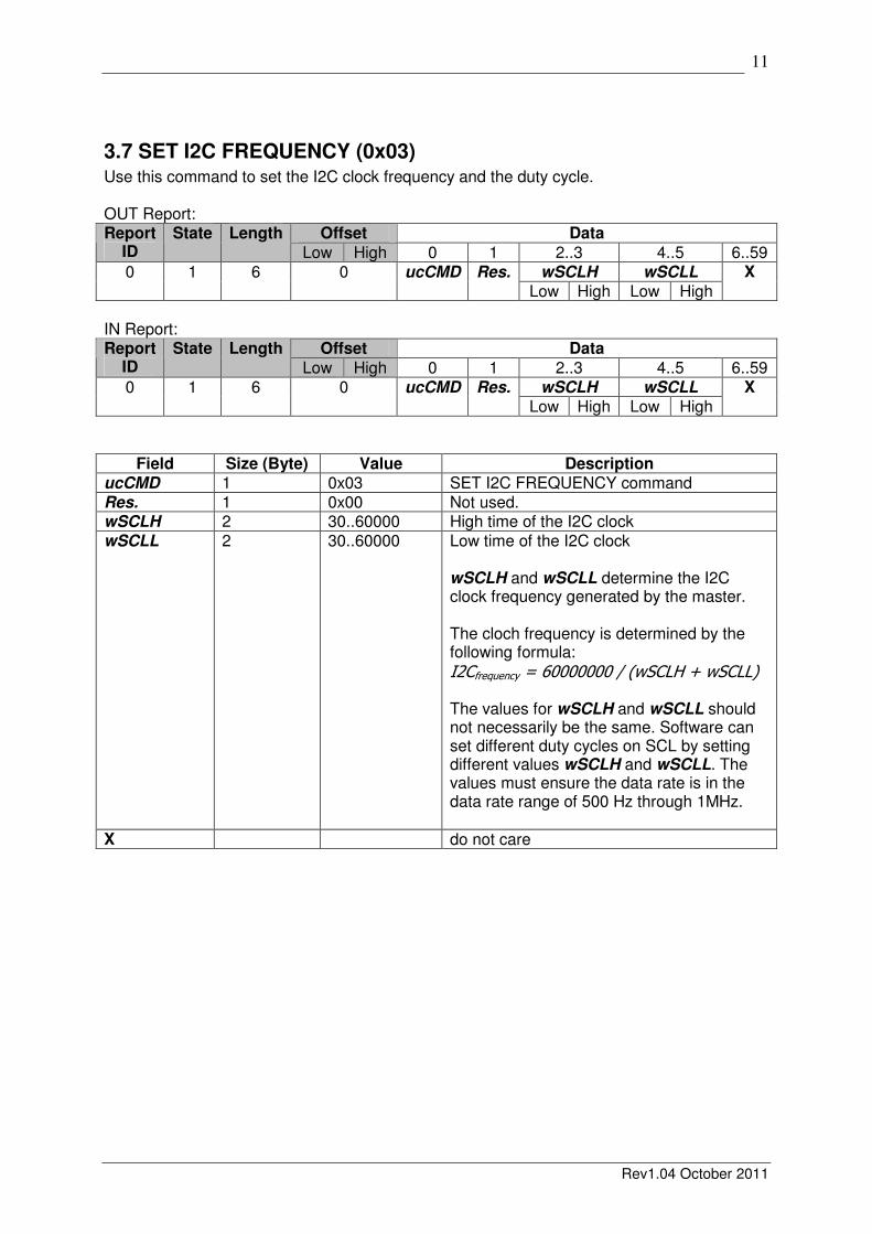
3.7 SET I2C FREQUENCY (0x03) Use this command to set the I2C clock frequency and the duty cycle. OUT Report:
Offset Data Report ID
State Length
Low High 0 1 2..3 4..5 6..59 wSCLH wSCLL 0 1 6 0 ucCMD Res.
Low High Low High
X
IN Report:
Offset Data Report ID
State Length
Low High 0 1 2..3 4..5 6..59 wSCLH wSCLL 0 1 6 0 ucCMD Res.
Low High Low High
X
Field Size (Byte) Value Description ucCMD 1 0x03 SET I2C FREQUENCY command Res. 1 0x00 Not used. wSCLH 2 30..60000 High time of the I2C clock wSCLL 2 30..60000 Low time of the I2C clock
wSCLH and wSCLL determine the I2C clock frequency generated by the master. The cloch frequency is determined by the following formula:
I2Cfrequency = 60000000 / (wSCLH + wSCLL) The values for wSCLH and wSCLL should not necessarily be the same. Software can set different duty cycles on SCL by setting different values wSCLH and wSCLL. The values must ensure the data rate is in the data rate range of 500 Hz through 1MHz.
X do not care

Rev1.04 October 2011
12
3.8 GET I2C FREQUENCY (0x04) Use this command to read the current value for I2C SCL clock frequency. OUT Report:
Offset Data Report ID
State Length
Low High 0 2..59 0 1 1 0 ucCMD X
IN Report:
Offset Data Report ID
State Length
Low High 0 1 2..3 4..5 6..59 wSCLH wSCLL 0 1 6 0 ucCMD Res.
Low High Low High
X
Field Size (Byte) Value Description
ucCMD 1 0x04 GET I2C FREQUENCY command Res. 1 0x00 Not used. wSCLH 2 30..60000 High time of the I2C clock wSCLL 2 30..60000 Low time of the I2C clock
wSCLH and wSCLL determine the I2C clock frequency generated by the master. The cloch frequency is determined by the following formula:
I2Cfrequency = 60000000 / (wSCLH + wSCLL)
X do not care

Rev1.04 October 2011
13
3.9 SET IRQ MODE (0x06) The converter has an interrupt input. e.g. if you use an IO-Expander, you could connect it’s interrupt output with the interrupt input of the converter. Then your software would recognize all events of the IO-Expander, if the state of the IOs changes. OUT Report:
Offset Data Report ID
State Length
Low High 0 1 2..59 0 1 2 0 ucCMD ucIRQMode X
IN Report:
Offset Data Report ID
State Length
Low High 0 1 2..59 0 1 2 0 ucCMD ucIRQMode X
Field Size (Byte) Value Description
ucCMD 1 0x06 SET IRQ MODE command 0x00 Disable interrupt 0x01 Enable interrupt. Falling-edge sensitive
ucIRQMode 1
0x02 Enable interrupt. Rising-edge sensitive X do not care
3.10 IRQ EVENT (0x09, 0xF6) This IN report is sent to the host, if the interrupt input is enabled and an interrupt is detected. IN Report:
Offset Data Report ID
State Length
Low High 0 1 2..59 0 1 2 0 ucID1 ucID2 X
Field Size (Byte) Value Description ucID1 1 0x09 IRQ EVENT 1. ID ucID2 1 0xF6 IRQ EVENT 2. ID X do not care
Rev1.04 October 2011
14
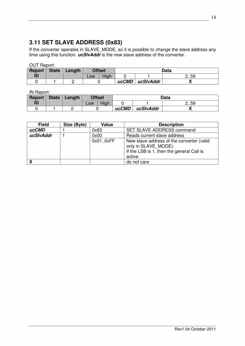
3.11 SET SLAVE ADDRESS (0x83) If the converter operates in SLAVE_MODE, so it is possible to change the slave address any time using this function. ucSlvAddr is the new slave address of the converter. OUT Report:
Offset Data Report ID
State Length
Low High 0 1 2..59 0 1 2 0 ucCMD ucSlvAddr X
IN Report:
Offset Data Report ID
State Length
Low High 0 1 2..59 0 1 2 0 ucCMD ucSlvAddr X
Field Size (Byte) Value Description ucCMD 1 0x83 SET SLAVE ADDRESS command
0x00 Reads current slave address ucSlvAddr 1 0x01..0xFF New slave address of the converter (valid
only in SLAVE_MODE). If the LSB is 1, then the general Call is active.
X do not care
Rev1.04 October 2011
15
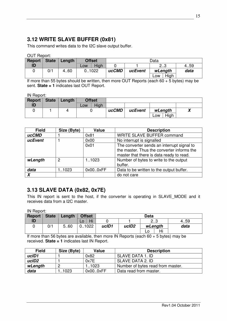
3.12 WRITE SLAVE BUFFER (0x81) This command writes data to the I2C slave output buffer. OUT Report:
Offset Data Report ID
State Length
Low High 0 1 2..3 4..59 wLength 0 0/1 4..60 0..1022 ucCMD ucEvent
Low High data
If more than 55 bytes should be written, then more OUT Reports (each 60 + 5 bytes) may be sent. State = 1 indicates last OUT Report. IN Report:
Offset Report ID
State Length
Low High wLength 0 1 4 0 ucCMD ucEvent
Low High X
Field Size (Byte) Value Description
ucCMD 1 0x81 WRITE SLAVE BUFFER command 0x00 No interrupt is signalled ucEvent 1 0x01 The converter sends an interrupt signal to
the master. Thus the converter informs the master that there is data ready to read.
wLength 2 1..1023 Number of bytes to write to the output buffer.
data 1..1023 0x00..0xFF Data to be written to the output buffer. X do not care
3.13 SLAVE DATA (0x82, 0x7E) This IN report is sent to the host, if the converter is operating in SLAVE_MODE and it receives data from a I2C master. IN Report:
Offset Data Report ID
State Length
Lo Hi 0 1 2..3 4..59
wLength 0 0/1 5..60 0..1022 ucID1 ucID2 Lo Hi
data
If more than 56 bytes are available, then more IN Reports (each 60 + 5 bytes) may be received. State = 1 indicates last IN Report.
Field Size (Byte) Value Description
ucID1 1 0x82 SLAVE DATA 1. ID ucID2 1 0x7E SLAVE DATA 2. ID wLength 2 1..1023 Number of bytes read from master. data 1..1023 0x00..0xFF Data read from master.

Rev1.04 October 2011
16
3.14 EXECUTE COMMAND DENIED (0xFE) This IN report is sent to the host, if the converter is operating in MASTER_MODE and the host is trying to send slave commands and vice versa. IN Report:
Offset Data Report ID
State Length
Low High 0 1..59 0 1 1 0 ucID X
Field Size (Byte) Value Description ucID 1 0xFE EXECUTE COMMAND DENIED ID X do not care
3.15 UNKNOWN COMMAND (0xFF) This IN report is sent to the host, if an unknown command was sent to the converter. IN Report:
Offset Data Report ID
State Length
Low High 0 1..59 0 1 1 0 ucCMD X
Field Size (Byte) Value Description
ucUCMD 1 0xFF UNKNOWN COMMAND ID X do not care

Rev1.04 October 2011
17
3.16 MEM WR 8BIT (0x20) writes 1 BYTE / 8Bit value into the non-volatile memory. OUT Report:
Offset Data Report ID
State Length
Low High 0 1 2..3 4 5..59 wAddr 0 1 5 0 ucCMD Res.
Lo Hi ucVal X
IN Report:
Offset Data Report ID
State Length
Lo Hi 0 1 2..59
0 1 2 0 ucCMD Ret X
Field Size (Byte) Value Description ucCMD 1 0x20 MEM WR 8BIT command Res. 1 0x00 Not used wAddr 2 0x0100..0x01FFF Memory address in the range 0x0100 to
0x1FFF. The first 256 Bytes are READ ONLY.
ucVal 1 0x00..0xFF 1 Byte / 8Bit value to write into Memory 0x00 Writing to memory: FAILED Ret 1 0x01 Writing to memory: SUCCESS
X do not care

Rev1.04 October 2011
18
3.17 MEM WR 16BIT (0x21) writes 1 WORD / 16Bit value into the non-volatile memory. OUT Report:
Offset Data Report ID
State Length
Low High 0 1 2..3 4..5 6..59 wAddr wVal 0 1 6 0 ucCMD Res. Lo Hi Lo Hi
X
IN Report:
Offset Data Report ID
State Length
Lo Hi 0 1 2..59
0 1 2 0 ucCMD Ret X
Field Size (Byte) Value Description ucCMD 1 0x21 MEM WR 8BIT command Res. 1 0x00 Not used wAddr 2 0x0100..0x01FFF Memory address in the range 0x0100 to
0x1FFF. The first 256 Bytes are READ ONLY.
wVal 2 0x0000..0xFFFF 1 Word / 16Bit value to write into Memory. 1
0x00 Writing to memory: FAILED Ret 1 0x01 Writing to memory: SUCCESS
X do not care

Rev1.04 October 2011
19
3.18 MEM WR 32BIT (0x22) writes 1 DWORD / 32Bit value into the non-volatile memory. OUT Report:
Offset Data Report ID
State Length
Low High 0 1 2..3 4..7 8..59 wAddr dwVal 0 1 8 0 ucCMD Res.
Lo Hi Lo..Hi
X
IN Report:
Offset Data Report ID
State Length
Lo Hi 0 1 2..59
0 1 2 0 ucCMD Ret X
Field Size (Byte) Value Description ucCMD 1 0x22 MEM WR 32BIT command Res. 1 0x00 Not used wAddr 2 0x0100..0x01FFF Memory address in the range 0x0100 to
0x1FFF. The first 256 Bytes are READ ONLY.
dwVal 4 0x00000000.. 0xFFFFFFFF
1 DWORD / 32Bit value to write into Memory. 1
0x00 Writing to memory: FAILED Ret 1 0x01 Writing to memory: SUCCESS
X do not care
Rev1.04 October 2011
20
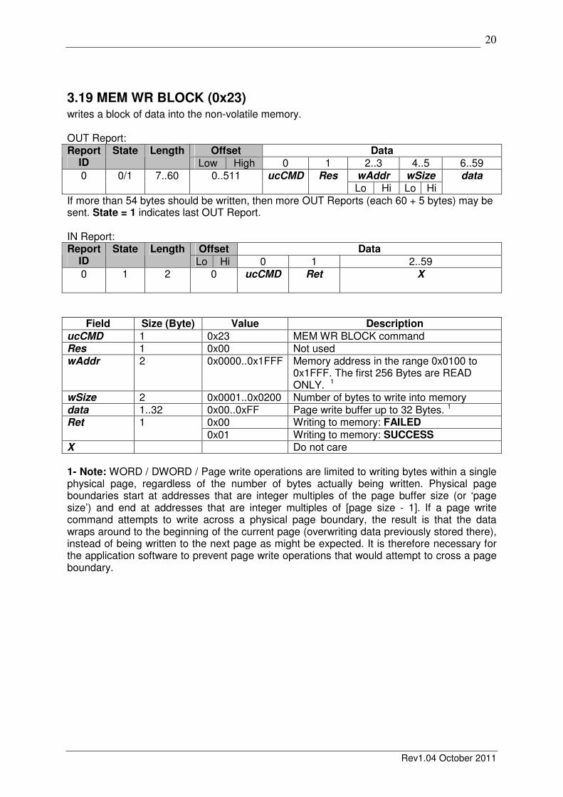
3.19 MEM WR BLOCK (0x23) writes a block of data into the non-volatile memory. OUT Report:
Offset Data Report ID
State Length
Low High 0 1 2..3 4..5 6..59 wAddr wSize 0 0/1 7..60 0..511 ucCMD Res Lo Hi Lo Hi
data
If more than 54 bytes should be written, then more OUT Reports (each 60 + 5 bytes) may be sent. State = 1 indicates last OUT Report. IN Report:
Offset Data Report ID
State Length
Lo Hi 0 1 2..59 0 1 2 0 ucCMD Ret X
Field Size (Byte) Value Description
ucCMD 1 0x23 MEM WR BLOCK command Res 1 0x00 Not used wAddr 2 0x0000..0x1FFF Memory address in the range 0x0100 to
0x1FFF. The first 256 Bytes are READ ONLY. 1
wSize 2 0x0001..0x0200 Number of bytes to write into memory data 1..32 0x00..0xFF Page write buffer up to 32 Bytes. 1
0x00 Writing to memory: FAILED Ret 1 0x01 Writing to memory: SUCCESS
X Do not care 1- Note: WORD / DWORD / Page write operations are limited to writing bytes within a single physical page, regardless of the number of bytes actually being written. Physical page boundaries start at addresses that are integer multiples of the page buffer size (or ‘page size’) and end at addresses that are integer multiples of [page size - 1]. If a page write command attempts to write across a physical page boundary, the result is that the data wraps around to the beginning of the current page (overwriting data previously stored there), instead of being written to the next page as might be expected. It is therefore necessary for the application software to prevent page write operations that would attempt to cross a page boundary.

Rev1.04 October 2011
21
3.20 MEM RD 8BIT (0x24) reads 1 BYTE / 8Bit value from memory. OUT Report:
Offset Data Report ID
State Length
Low High 0 1 2..3 4..59 wAddr 0 1 4 0 ucCMD Res.
Lo Hi
X
IN Report:
Offset Data Report ID
State Length
Lo Hi 0 1 2 3..59
0 1 3 0 ucCMD Ret ucVal X
Field Size (Byte) Value Description ucCMD 1 0x24 MEM RD 8BIT command Res 1 0x00 Not used wAddr 2 0x0000..0x1FFF Memory address in the range 0x0000 to
0x1FFF. ucVal 1 0x00..0xFF 8Bit value read from memory.
0x00 Reading from memory: FAILED Ret 1 0x01 Reading from memory: SUCCESS
X Do not care
3.21 MEM RD 16BIT (0x25) reads 1 WORD / 16Bit value from memory. OUT Report:
Offset Data Report ID
State Length
Low High 0 1 2..3 4..59 wAddr 0 1 4 0 ucCMD Res.
Lo Hi
X
IN Report:
Offset Data Report ID
State Length
Lo Hi 0 1 2..3 4..59 wVal 0 1 4 0 ucCMD Ret
Lo Hi
X
Field Size (Byte) Value Description
ucCMD 1 0x25 MEM RD 16BIT command Res 1 0x00 Not used. wAddr 2 0x0000..0x1FFF Memory address in the range 0x0000 to
0x1FFF. wVal 2 0x0000..0xFFFF 16Bit value read from memory.
0x00 Reading from memory: FAILED Ret 1 0x01 Reading from memory: SUCCESS
X Do not casre

Rev1.04 October 2011
22
3.22 MEM RD 32BIT (0x26) reads 1 DWORD / 32Bit value from memory. OUT Report:
Offset Data Report ID
State Length
Low High 0 1 2..3 4..59 wAddr 0 1 4 0 ucCMD Res.
Lo Hi
X
IN Report:
Offset Data Report ID
State Length
Lo Hi 0 1 2..5 6..59
dwVal 0 1 6 0 ucCMD Ret
Lo Hi
X
Field Size (Byte) Value Description
CMD 1 0x26 MEM RD 32BIT command wAddr 2 0x0000..0x1FFF Memory address in the range 0x0000 to
0x1FFF. Res 1 0x00 Not used dwVal 4 0x00000000..
0xFFFFFFFF 32Bit value read from memory.
0x00 Reading from memory: FAILED Ret 1 0x01 Reading from memory: SUCCESS
X Do not care

Rev1.04 October 2011
23
3.23 MEM RD BLOCK (0x27) reads a block of data (V1.03: up to 512 Bytes; V1.04 and later: 1024 Bytes) from memory. OUT Report:
Offset Data Report ID
State Length
Low High 0 1 2..3 4..5 6..59 wAddr wSize 0 0/1 6 0..1023 ucCMD Res Lo Hi Lo Hi
X
IN Report:
Offset Data Report ID
State Length
Lo HI 0 1 2..3 4..59 wSize 0 0/1 4..60 0..1023 ucCMD Ret
Lo Hi data
Field Size (Byte) Value Description
ucCMD 1 0x27 MEM READ BLOCK command Res 1 0x00 Not used wAddr 2 0x0000..0x1FFF Memory address in the range 0x0000 to
0x1FFF. wSize 2 0x0001..0x0200 Number of Bytes to read from memory. data 0..1023 * 0x00..0xFF Data read from memory.
0x00 Reading from memory: FAILED Ret 1 0x01 Reading from memory: SUCCESS
X Do not care * Version 1.04 and later. V1.03 supports up to 512 blocks only.
3.24 SAVE SETTINGS (0x28) the settings (operation mode, slave address and SCL frequency) are stored into onboard memory. OUT Report:
Offset Data Report ID
State Length
Low High 0 2..59
0 1 1 0 ucCMD X
IN Report:
Offset Data Report ID
State Length
Low High 0 1 2..59 0 1 2 0 ucCMD Ret X
Field Size (Byte) Value Description
ucCMD 1 0x28 SAVE SETTINGS command 0x00 Save Settings: FAILED Ret 1 0x01 Save Settings: SUCCESS
X do not care

Rev1.04 October 2011
24
3.25 RESET SETTINGS (0x29) loads factory (default) settings: MASTER_MODE SLAVE ADDRESS = 0x00 SCL FREQUENCY = 100 kHz. (wSCLL = 0x012C and wSCLH = 0x012C) OUT Report:
Offset Data Report ID
State Length
Low High 0 2..59
0 1 1 0 ucCMD X
IN Report:
Offset Data Report ID
State Length
Low High 0 1 2..59 0 1 2 0 ucCMD Ret X
Field Size (Byte) Value Description
ucCMD 1 0x29 RESET SETTINGS command 0x00 Reset Settings: FAILED Ret 1 0x01 Reset Settings: SUCCESS
X do not care