Embed Size (px)
Citation preview
Document Number: 327405-001
Intel® Xeon® and Intel® Core™ Processors For Communications InfrastructureDatasheet - Volume 1 of 2
Supporting:
Intel® Xeon® Processor E3-1125C
Intel® Xeon® Processor E3-1105C
Intel® Core™ i3 Processor 2115C
Intel® Pentium® Processor B915C
Intel® Celeron® Processor 725C
Document #324803 - 2nd Generation Intel® Core™ Processor Family Mobile Datasheet - Volume 2 completes the documentation set and contains additional product information.
May 2012
Intel® Xeon® and Intel® Core™ Processors For Communications InfrastructureDatasheet - Volume 1 of 2 May 20122 Document Number: 327405-001
Legal Lines and DisclaimersINFORMATION IN THIS DOCUMENT IS PROVIDED IN CONNECTION WITH INTEL PRODUCTS. NO LICENSE, EXPRESS OR IMPLIED, BY ESTOPPEL OR OTHERWISE, TO ANY INTELLECTUAL PROPERTY RIGHTS IS GRANTED BY THIS DOCUMENT. EXCEPT AS PROVIDED IN INTEL'S TERMS AND CONDITIONS OF SALE FOR SUCH PRODUCTS, INTEL ASSUMES NO LIABILITY WHATSOEVER AND INTEL DISCLAIMS ANY EXPRESS OR IMPLIED WARRANTY, RELATING TO SALE AND/OR USE OF INTEL PRODUCTS INCLUDING LIABILITY OR WARRANTIES RELATING TO FITNESS FOR A PARTICULAR PURPOSE, MERCHANTABILITY, OR INFRINGEMENT OF ANY PATENT, COPYRIGHT OR OTHER INTELLECTUAL PROPERTY RIGHT.A "Mission Critical Application" is any application in which failure of the Intel Product could result, directly or indirectly, in personal injury or death. SHOULD YOU PURCHASE OR USE INTEL'S PRODUCTS FOR ANY SUCH MISSION CRITICAL APPLICATION, YOU SHALL INDEMNIFY AND HOLD INTEL AND ITS SUBSIDIARIES, SUBCONTRACTORS AND AFFILIATES, AND THE DIRECTORS, OFFICERS, AND EMPLOYEES OF EACH, HARMLESS AGAINST ALL CLAIMS COSTS, DAMAGES, AND EXPENSES AND REASONABLE ATTORNEYS' FEES ARISING OUT OF, DIRECTLY OR INDIRECTLY, ANY CLAIM OF PRODUCT LIABILITY, PERSONAL INJURY, OR DEATH ARISING IN ANY WAY OUT OF SUCH MISSION CRITICAL APPLICATION, WHETHER OR NOT INTEL OR ITS SUBCONTRACTOR WAS NEGLIGENT IN THE DESIGN, MANUFACTURE, OR WARNING OF THE INTEL PRODUCT OR ANY OF ITS PARTS.Intel may make changes to specifications and product descriptions at any time, without notice. Designers must not rely on the absence or characteristics of any features or instructions marked "reserved" or "undefined." Intel reserves these for future definition and shall have no responsibility whatsoever for conflicts or incompatibilities arising from future changes to them. The information here is subject to change without notice. Do not finalize a design with this information.The products described in this document may contain design defects or errors known as errata which may cause the product to deviate from published specifications. Current characterized errata are available on request.Contact your local Intel sales office or your distributor to obtain the latest specifications and before placing your product order.Copies of documents which have an order number and are referenced in this document, or other Intel literature, may be obtained by calling 1-800-548-4725, or go to: http://www.intel.com/#/en_US_01Intel processor numbers are not a measure of performance. Processor numbers differentiate features within each processor family, not across different processor families. Go to: http://www.intel.com/products/processor%5Fnumber/BunnyPeople, Celeron, Celeron Inside, Centrino, Centrino Inside, Cilk, Core Inside, i960, Intel, the Intel logo, Intel AppUp, Intel Atom, Intel Atom Inside, Intel Core, Intel Inside, Intel Insider, the Intel Inside logo, Intel NetBurst, Intel NetMerge, Intel NetStructure, Intel SingleDriver, Intel SpeedStep, Intel Sponsors of Tomorrow., the Intel Sponsors of Tomorrow. logo, Intel StrataFlash, Intel vPro, Intel XScale, InTru, the InTru logo, the InTru Inside logo, InTru soundmark, Itanium, Itanium Inside, MCS, MMX, Moblin, Pentium, Pentium Inside, Puma, skoool, the skoool logo, Sound Mark, The Creators Project, The Journey Inside, Thunderbolt, vPro Inside, VTune, Xeon, and Xeon Inside are trademarks of Intel Corporation in the U.S. and/or other countries.*Other names and brands may be claimed as the property of others.Copyright © 2012, Intel Corporation. All rights reserved.
Intel® Xeon® and Intel® Core™ Processors For Communications InfrastructureMay 2012 Datasheet - Volume 1 of 2Document Number: 327405-001 3
Revision History
Revision History
Date Revision Description
May 2012 001 Initial release
Contents
Intel® Xeon® and Intel® Core™ Processors For Communications InfrastructureDatasheet - Volume 1 of 2 May 20124 Document Number: 327405-001
Contents
1.0 Introduction ............................................................................................................111.1 Purpose / Scope / Audience.................................................................................111.2 Related Documents ............................................................................................111.3 Terminology......................................................................................................13
2.0 Product Overview ....................................................................................................152.1 Product Features ...............................................................................................172.2 Processor Details ...............................................................................................172.3 Supported Technologies......................................................................................172.4 Interface Features .............................................................................................17
2.4.1 System Memory Support .........................................................................172.4.2 PCI Express*..........................................................................................182.4.3 Direct Media Interface (DMI) ....................................................................202.4.4 Platform Environment Control Interface (PECI) ...........................................20
2.5 Power Management Support................................................................................212.5.1 Processor Core .......................................................................................212.5.2 System .................................................................................................212.5.3 Memory Controller ..................................................................................212.5.4 PCI Express*..........................................................................................212.5.5 DMI ......................................................................................................21
2.6 Thermal Management Support.............................................................................212.7 Package ...........................................................................................................212.8 Testability.........................................................................................................21
3.0 Interfaces ................................................................................................................233.1 System Memory Interface ...................................................................................23
3.1.1 System Memory Configurations Supported .................................................233.1.2 System Memory Timing Support ...............................................................263.1.3 System Memory Organization Modes .........................................................273.1.4 Rules for Populating Memory Slots ............................................................283.1.5 Technology Enhancements of Intel® Fast Memory Access (Intel® FMA) ..........283.1.6 Data Scrambling.....................................................................................293.1.7 DRAM Clock Generation ...........................................................................29
3.2 PCI Express* Interface .......................................................................................293.2.1 PCI Express* Architecture........................................................................303.2.2 PCI Express* Configuration Mechanism......................................................323.2.3 PCI Express* Port Bifurcation ...................................................................323.2.4 PCI Express* Lanes Connection ................................................................343.2.5 Configuring PCIe* Lanes..........................................................................353.2.6 Lane Reversal on PCIe* Interface..............................................................36
3.3 Direct Media Interface ........................................................................................363.3.1 DMI Error Flow .......................................................................................363.3.2 Processor/PCH Compatibility Assumptions ..................................................363.3.3 DMI Link Down.......................................................................................36
3.4 Platform Environment Control Interface (PECI) ......................................................373.5 Interface Clocking..............................................................................................37
3.5.1 Internal Clocking Requirements ................................................................37
4.0 Technologies............................................................................................................394.1 Intel® Virtualization Technology ..........................................................................39
4.1.1 Intel® VT-x Objectives ............................................................................394.1.2 Intel® VT-x Features ...............................................................................394.1.3 Intel® VT-d Objectives ............................................................................40
Intel® Xeon® and Intel® Core™ Processors For Communications InfrastructureMay 2012 Datasheet - Volume 1 of 2Document Number: 327405-001 5
Contents
4.1.4 Intel® VT-d Features .............................................................................. 404.1.5 Intel® VT-d Features Not Supported ......................................................... 41
4.2 Intel® Hyper-Threading Technology..................................................................... 414.3 Intel® Advanced Vector Extensions (Intel® AVX) ................................................... 414.4 Intel® Advanced Encryption Standard New Instructions (Intel® AES-NI) ................... 42
4.4.1 PCLMULQDQ Instruction .......................................................................... 424.5 Intel® 64 Architecture x2APIC............................................................................. 42
5.0 Processor SKUs ....................................................................................................... 455.1 Overview ......................................................................................................... 45
5.1.1 SKU Features......................................................................................... 45
6.0 Power Management ................................................................................................. 476.1 ACPI States Supported....................................................................................... 48
6.1.1 System States ....................................................................................... 486.1.2 Processor Core/Package Idle States .......................................................... 486.1.3 Integrated Memory Controller States ........................................................ 486.1.4 PCIe* Link States................................................................................... 496.1.5 DMI States ............................................................................................ 496.1.6 Interface State Combinations................................................................... 49
6.2 Processor Core Power Management...................................................................... 496.2.1 Enhanced Intel SpeedStep® Technology ................................................... 506.2.2 Low-Power Idle States ............................................................................ 506.2.3 Requesting Low-Power Idle States ............................................................ 516.2.4 Core C-states ........................................................................................ 526.2.5 Package C-States ................................................................................... 53
6.3 IMC Power Management..................................................................................... 576.3.1 Disabling Unused System Memory Outputs ................................................ 576.3.2 DRAM Power Management and Initialization ............................................... 57
6.4 PCIe* Power Management .................................................................................. 596.5 DMI Power Management..................................................................................... 596.6 Thermal Power Management............................................................................... 59
7.0 Thermal Management .............................................................................................. 617.1 Thermal Design Power (TDP) and
Junction Temperature (TJ).................................................................................. 617.2 Thermal and Power Specifications........................................................................ 617.3 Thermal Management Features ........................................................................... 63
7.3.1 Processor Package Thermal Features......................................................... 637.3.2 Processor Core Specific Thermal Features .................................................. 687.3.3 Memory Controller Specific Thermal Features ............................................. 687.3.4 Platform Environment Control Interface (PECI)........................................... 69
8.0 Signal Description ................................................................................................... 718.1 System Memory Interface .................................................................................. 718.2 Memory Reference and Compensation.................................................................. 748.3 Reset and Miscellaneous Signals.......................................................................... 748.4 PCI Express* Based Interface Signals................................................................... 758.5 DMI................................................................................................................. 758.6 PLL Signals....................................................................................................... 768.7 TAP Signals ...................................................................................................... 768.8 Error and Thermal Protection .............................................................................. 778.9 Power Sequencing ............................................................................................. 788.10 Processor Power and Ground Signals.................................................................... 788.11 Sense Pins ....................................................................................................... 798.12 Future Compatibility .......................................................................................... 798.13 Processor Internal Pull Up/Pull Down.................................................................... 79
Contents
Intel® Xeon® and Intel® Core™ Processors For Communications InfrastructureDatasheet - Volume 1 of 2 May 20126 Document Number: 327405-001
9.0 Electrical Specifications ...........................................................................................819.1 Power and Ground Pins.......................................................................................819.2 Decoupling Guidelines ........................................................................................81
9.2.1 Voltage Rail Decoupling ...........................................................................819.3 Processor Clocking (BCLK, BCLK#).......................................................................82
9.3.1 PLL Power Supply ...................................................................................829.4 Serial Voltage Identification (SVID) ......................................................................829.5 System Agent (SA) Vcc VID ................................................................................899.6 Reserved or Unused Signals ................................................................................909.7 Signal Groups ...................................................................................................909.8 Test Access Port (TAP) Connection .......................................................................929.9 Storage Conditions Specifications.........................................................................929.10 DC Specifications...............................................................................................93
9.10.1 Voltage and Current Specifications ............................................................949.10.2 Platform Environmental Control Interface DC Specifications ..........................99
9.11 AC Specifications .............................................................................................1019.11.1 DDR3 AC Specifications .........................................................................1039.11.2 PCI Express* AC Specification ................................................................1079.11.3 Miscellaneous AC Specifications ..............................................................1089.11.4 TAP Signal Group AC Specifications .........................................................1089.11.5 SVID Signal Group AC Specifications .......................................................109
9.12 Processor AC Timing Waveforms ........................................................................1099.13 Signal Quality..................................................................................................114
9.13.1 Input Reference Clock Signal Quality Specifications ...................................1159.13.2 DDR3 Signal Quality Specifications..........................................................1159.13.3 I/O Signal Quality Specifications .............................................................115
9.14 Overshoot/Undershoot Guidelines ......................................................................1159.14.1 VCC Overshoot Specification ..................................................................1159.14.2 Overshoot/Undershoot Magnitude ...........................................................1169.14.3 Overshoot/Undershoot Pulse Duration .....................................................116
10.0 Processor Ball and Package Information ................................................................11910.1 Processor Ball Assignments ...............................................................................11910.2 Package Mechanical Information ........................................................................146
11.0 Processor Configuration Registers .........................................................................15111.1 ERRSTS - Error Status......................................................................................15211.2 ERRCMD - Error Command................................................................................15311.3 SMICMD - SMI Command..................................................................................15411.4 SCICMD - SCI Command ..................................................................................15511.5 ECCERRLOG0_C0 - ECC Error Log 0 ...................................................................15511.6 ECCERRLOG1_C0 - ECC Error Log 1 ...................................................................15611.7 ECCERRLOG0_C1 - ECC Error Log 0 ...................................................................15711.8 ECCERRLOG1_C1 - ECC Error Log 1 ...................................................................15811.9 MAD_DIMM_CH0 - Address Decode Channel 0 .....................................................15811.10 MAD_DIMM_CH1 - Address Decode Channel 1 .....................................................16011.11 Error Detection and Correction ..........................................................................161
Figures2-1 Crystal Forest Platform Example Block Diagram ......................................................163-1 Intel® Flex Memory Technology Operation.............................................................283-2 PCI Express* Layering Diagram ............................................................................303-3 Packet Flow through the Layers ............................................................................313-4 PCI Express* Related Register Structures...............................................................32
Intel® Xeon® and Intel® Core™ Processors For Communications InfrastructureMay 2012 Datasheet - Volume 1 of 2Document Number: 327405-001 7
Contents
3-5 PCI Express* PCI Port Bifurcation ......................................................................... 333-6 PCIe* Typical Operation 16 Lanes Mapping ............................................................ 346-1 Power States ..................................................................................................... 476-2 Idle Power Management Breakdown of the Processor Cores ..................................... 506-3 Thread and Core C-State Entry and Exit ................................................................ 516-4 Package C-State Entry and Exit ............................................................................ 557-1 Frequency and Voltage Ordering........................................................................... 649-1 Example of PECI Host-Client Connection.............................................................. 1009-2 Input Device Hysteresis .................................................................................... 1019-3 Differential Clock – Differential Measurements...................................................... 1109-4 Differential Clock – Single Ended Measurements ................................................... 1119-5 DDR3 Command / Control and Clock Timing Waveform ......................................... 1119-6 DDR3 Receiver Eye Mask................................................................................... 1129-7 DDR3 Clock to DQS Skew Timing Waveform ........................................................ 1129-8 PCI Express* Receiver Eye Margins..................................................................... 1139-9 TAP Valid Delay Timing Waveform ...................................................................... 1139-10 Test Reset (TRST#), Async Input, and PROCHOT# Timing Waveform ...................... 1149-11 THERMTRIP# Power Down Sequence .................................................................. 1149-12 VCC Overshoot Example Waveform..................................................................... 1169-13 Maximum Acceptable Overshoot/Undershoot Waveform......................................... 11710-1 Ball Map (Bottom View, Upper Left Side) ............................................................. 14210-2 Ball Map (Bottom View, Upper Right Side) ........................................................... 14310-3 Ball Map (Bottom View, Lower Left Side) ............................................................. 14410-4 Ball Map (Bottom View, Lower Right Side) ........................................................... 14510-5 Processor 4-Core Die Mechanical Package............................................................ 14710-6 Processor 2-Core Die / 1-Core Die Mechanical Package.......................................... 148
Tables1-1 Processor Documents ......................................................................................... 111-2 Cave Creek PCH Documents ................................................................................ 121-3 Public Specifications ........................................................................................... 121-4 Terminology ...................................................................................................... 133-1 Supported UDIMM Module Configurations1, 2......................................................... 243-2 Supported SO-DIMM Module Configurations1, 2...................................................... 253-3 Supported Memory Down Configurations 1 ............................................................ 263-4 DDR3 System Memory Timing Support.................................................................. 273-5 Hardware Straps for PCIe* Controller Enabling (Port 1 Only) .................................... 353-6 Hardware Straps for Normal/Reversed Operation of PCIe* Lanes .............................. 363-7 Reference Clock ................................................................................................. 375-1 Base Features by SKU......................................................................................... 456-1 System States ................................................................................................... 486-2 Processor Core/Package State Support.................................................................. 486-3 Integrated Memory Controller States .................................................................... 486-4 PCIe* Link States............................................................................................... 496-5 DMI States ........................................................................................................ 496-6 G, S and C State Combinations ............................................................................ 496-7 Coordination of Thread Power States at the Core Level............................................ 516-8 P_LVLx to MWAIT Conversion............................................................................... 526-9 Coordination of Core Power States at the Package Level .......................................... 547-1 TDP Specifications .............................................................................................. 627-2 Junction Temperature Specification....................................................................... 628-1 Signal Description Buffer Types............................................................................ 718-2 Memory Channel A ............................................................................................. 718-3 Memory Channel B ............................................................................................. 72
Contents
Intel® Xeon® and Intel® Core™ Processors For Communications InfrastructureDatasheet - Volume 1 of 2 May 20128 Document Number: 327405-001
8-4 Memory Reference and Compensation ...................................................................748-5 Reset and Miscellaneous Signals ...........................................................................748-6 PCI Express* Interface Signals .............................................................................758-7 DMI - Processor to PCH Serial Interface .................................................................758-8 PLL Signals ........................................................................................................768-9 TAP Signals........................................................................................................768-10 Error and Thermal Protection................................................................................778-11 Power Sequencing ..............................................................................................788-12 Processor Power Signals ......................................................................................788-13 Sense Pins.........................................................................................................798-14 Future Compatibility............................................................................................798-15 Processor Internal Pull Up/Pull Down .....................................................................799-1 IMVP7 Voltage Identification Definition ..................................................................829-2 VCCSA_VID Configuration....................................................................................899-3 Signal Groups ....................................................................................................909-4 Storage Condition Ratings....................................................................................939-5 Processor Core (VCC) DC Voltage and Current Specifications ....................................949-6 Processor Uncore (VCCIO) Supply DC Voltage and Current Specifications ...................969-7 Memory Controller (VDDQ) Supply DC Voltage and Current Specifications ..................969-8 System Agent (VCCSA) Supply DC Voltage and Current Specifications .......................969-9 Processor PLL (VCCPLL) Supply DC Voltage and Current Specifications.......................979-10 DDR3 Signal Group DC Specifications ....................................................................979-11 Control Sideband and TAP Signal Group DC Specifications ........................................989-12 PCI Express* DC Specifications.............................................................................999-13 PECI DC Electrical Limits....................................................................................1009-14 Differential Clocks (SSC on) ...............................................................................1029-15 Differential Clocks (SSC off) ...............................................................................1029-16 Processor Clock Jitter Specifications (cycle-cycle)..................................................1029-17 System Reference Clock DC and AC Specifications.................................................1029-18 DDR3 Electrical Characteristics and AC Timings at 1066 MT/s,
VDDQ = 1.5 V ±0.075 V....................................................................................1049-19 DDR3 Electrical Characteristics and AC Timings at 1333 MT/s,
VDDQ = 1.5 V ±0.075 V....................................................................................1059-20 DDR3 Electrical Characteristics and AC Timings at 1600 MT/s,
VDDQ = 1.5 V ±0.075 V....................................................................................1069-21 PCI Express* AC Specification ............................................................................1079-22 Miscellaneous AC Specifications ..........................................................................1089-23 TAP Signal Group AC Specifications .....................................................................1089-24 SVID Signal Group AC Specifications ...................................................................1099-25 VCC Overshoot Specifications .............................................................................1159-26 Processor Overshoot/Undershoot Specifications ....................................................11610-1 Alphabetical Ball Listing .....................................................................................12010-2 Alphabetical Signal Listing..................................................................................13111-1 Register Terminology ........................................................................................15111-2 Register Terminology Attribute Modifier ...............................................................15211-3 Error Status Register.........................................................................................15211-4 Error Command Registers ..................................................................................15411-5 SMI Command Registers....................................................................................15411-6 SCI Command Registers ....................................................................................15511-7 Channel 0 ECC Error Log 0.................................................................................15611-8 Channel 0 ECC Error Log 1.................................................................................15711-9 Channel 1 ECC Error Log 0.................................................................................15711-10 Channel 1 ECC Error Log 1.................................................................................15811-11 Address Decode Channel 0.................................................................................15911-12 Address Decode Channel 1.................................................................................160
Intel® Xeon® and Intel® Core™ Processors For Communications InfrastructureMay 2012 Datasheet - Volume 1 of 2Document Number: 327405-001 9
Contents
11-13 Error Syndrome - ERRSYND............................................................................... 161
§ §

Contents
Intel® Xeon® and Intel® Core™ Processors For Communications InfrastructureDatasheet - Volume 1 of 2 May 201210 Document Number: 327405-001
Introduction
Intel® Xeon® and Intel® Core™ Processors For Communications InfrastructureMay 2012 Datasheet 1 of 2Document Number: 327405-001 11
1.0 Introduction
1.1 Purpose / Scope / AudienceThis document is to be used by Intel customers in place of the 2nd Generation Intel® Core™ Processor Family Mobile Datasheet - Volume 1 document #324803.
This document contains the following processor information:• DC and AC electrical specifications• Differential signaling specifications• Pinout and signal definitions• Interface functional descriptions• Additional product feature information• Configuration registers pertinent to the implementation and operation of the
processor on its respective platform.
For register details, see the latest version of the 2nd Generation Intel® Core™ Processor Family Mobile Datasheet – Volume 2.
1.2 Related DocumentsSee the following documents for additional information.
Table 1-1. Processor Documents
Document Document Number/ Location
2nd Generation Intel® Core™ Processor Family Mobile Datasheet - Volume 2 of 2
324803; http://www.intel.com/content/dam/doc/datasheet/2nd-
gen-core-family-mobile-vol-2-datasheet.pdf
Intel® Xeon® and Intel® Core™ Processors For Communications Infrastructure Thermal/Mechanical Design Guide
327397; http://download.intel.com/
embedded/processors/thermalguide/327397.pdf
Intel® Xeon® and Intel® Core™ Processors For Communications Infrastructure Specification Update
327335; http://download.intel.com/
embedded/processor/specupdate/327335.pdf
Introduction
Intel® Xeon® and Intel® Core™ Processors For Communications InfrastructureDatasheet 1 of 2 May 201212 Document Number: 327405-001
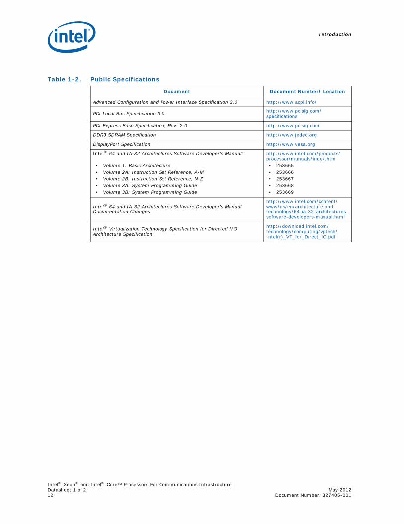
Table 1-2. Public Specifications
Document Document Number/ Location
Advanced Configuration and Power Interface Specification 3.0 http://www.acpi.info/
PCI Local Bus Specification 3.0 http://www.pcisig.com/specifications
PCI Express Base Specification, Rev. 2.0 http://www.pcisig.com
DDR3 SDRAM Specification http://www.jedec.org
DisplayPort Specification http://www.vesa.org
Intel® 64 and IA-32 Architectures Software Developer's Manuals:
• Volume 1: Basic Architecture• Volume 2A: Instruction Set Reference, A-M• Volume 2B: Instruction Set Reference, N-Z• Volume 3A: System Programming Guide • Volume 3B: System Programming Guide
http://www.intel.com/products/processor/manuals/index.htm• 253665• 253666• 253667• 253668• 253669
Intel® 64 and IA-32 Architectures Software Developer's Manual Documentation Changes
http://www.intel.com/content/www/us/en/architecture-and-technology/64-ia-32-architectures-software-developers-manual.html
Intel® Virtualization Technology Specification for Directed I/O Architecture Specification
http://download.intel.com/technology/computing/vptech/Intel(r)_VT_for_Direct_IO.pdf
Introduction
Intel® Xeon® and Intel® Core™ Processors For Communications InfrastructureMay 2012 Datasheet 1 of 2Document Number: 327405-001 13
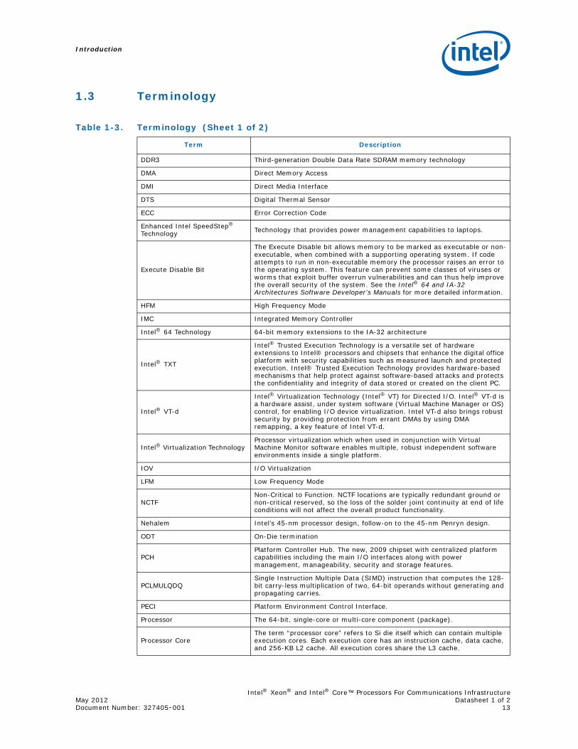
1.3 Terminology
Table 1-3. Terminology (Sheet 1 of 2)
Term Description
DDR3 Third-generation Double Data Rate SDRAM memory technology
DMA Direct Memory Access
DMI Direct Media Interface
DTS Digital Thermal Sensor
ECC Error Correction Code
Enhanced Intel SpeedStep® Technology Technology that provides power management capabilities to laptops.
Execute Disable Bit
The Execute Disable bit allows memory to be marked as executable or non-executable, when combined with a supporting operating system. If code attempts to run in non-executable memory the processor raises an error to the operating system. This feature can prevent some classes of viruses or worms that exploit buffer overrun vulnerabilities and can thus help improve the overall security of the system. See the Intel® 64 and IA-32 Architectures Software Developer's Manuals for more detailed information.
HFM High Frequency Mode
IMC Integrated Memory Controller
Intel® 64 Technology 64-bit memory extensions to the IA-32 architecture
Intel® TXT
Intel® Trusted Execution Technology is a versatile set of hardware extensions to Intel® processors and chipsets that enhance the digital office platform with security capabilities such as measured launch and protected execution. Intel® Trusted Execution Technology provides hardware-based mechanisms that help protect against software-based attacks and protects the confidentiality and integrity of data stored or created on the client PC.
Intel® VT-d
Intel® Virtualization Technology (Intel® VT) for Directed I/O. Intel® VT-d is a hardware assist, under system software (Virtual Machine Manager or OS) control, for enabling I/O device virtualization. Intel VT-d also brings robust security by providing protection from errant DMAs by using DMA remapping, a key feature of Intel VT-d.
Intel® Virtualization Technology Processor virtualization which when used in conjunction with Virtual Machine Monitor software enables multiple, robust independent software environments inside a single platform.
IOV I/O Virtualization
LFM Low Frequency Mode
NCTFNon-Critical to Function. NCTF locations are typically redundant ground or non-critical reserved, so the loss of the solder joint continuity at end of life conditions will not affect the overall product functionality.
Nehalem Intel’s 45-nm processor design, follow-on to the 45-nm Penryn design.
ODT On-Die termination
PCHPlatform Controller Hub. The new, 2009 chipset with centralized platform capabilities including the main I/O interfaces along with power management, manageability, security and storage features.
PCLMULQDQSingle Instruction Multiple Data (SIMD) instruction that computes the 128-bit carry-less multiplication of two, 64-bit operands without generating and propagating carries.
PECI Platform Environment Control Interface.
Processor The 64-bit, single-core or multi-core component (package).
Processor CoreThe term “processor core” refers to Si die itself which can contain multiple execution cores. Each execution core has an instruction cache, data cache, and 256-KB L2 cache. All execution cores share the L3 cache.
Introduction
Intel® Xeon® and Intel® Core™ Processors For Communications InfrastructureDatasheet 1 of 2 May 201214 Document Number: 327405-001
§ §
PCU Power Control Unit
RankA unit of DRAM corresponding four to eight devices in parallel, ignoring ECC. These devices are usually, but not always, mounted on a single side of a DIMM.
SCI System Control Interrupt. Used in ACPI protocol.
Storage Conditions
A non-operational state. The processor may be installed in a platform, in a tray, or loose. Processors may be sealed in packaging or exposed to free air. Under these conditions, processor landings should not be connected to any supply voltages, have any I/Os biased or receive any clocks. Upon exposure to “free air” (i.e., unsealed packaging or a device removed from packaging material) the processor must be handled in accordance with moisture sensitivity labeling (MSL) as indicated on the packaging material.
SVID Serial Voltage Identification
System AgentConsists of all the uncore functions within the processor other than the cores and cache. This includes the integrated memory controller, PCIe controller, PCU, etc.
TDP Thermal Design Power.
TDCThermal Design Current is the maximum current that the VR must be thermally capable of sustaining indefinitely in the worst-case thermal environment defined for the platform.
TPM Trusted Platform Module
VCC Processor core power supply.
VSS Processor ground.
VTT L3 shared cache, memory controller, and processor I/O power rail.
VDDQ DDR3 power rail.
VCCSA System Agent (memory controller, DMI and PCIe controllers) power supply
VCCIO High Frequency I/O logic power supply
VCCPLL PLL power supply
x1 Refers to a Link or Port with one Physical Lane.
x4 Refers to a Link or Port with four Physical Lanes.
x8 Refers to a Link or Port with eight Physical Lanes.
x16 Refers to a Link or Port with sixteen Physical Lanes.
Table 1-3. Terminology (Sheet 2 of 2)
Term Description
Product Overview
Intel® Xeon® and Intel® Core™ Processors For Communications InfrastructureMay 2012 Datasheet - Volume 1 of 2Document Number: 327405-001 15
2.0 Product Overview
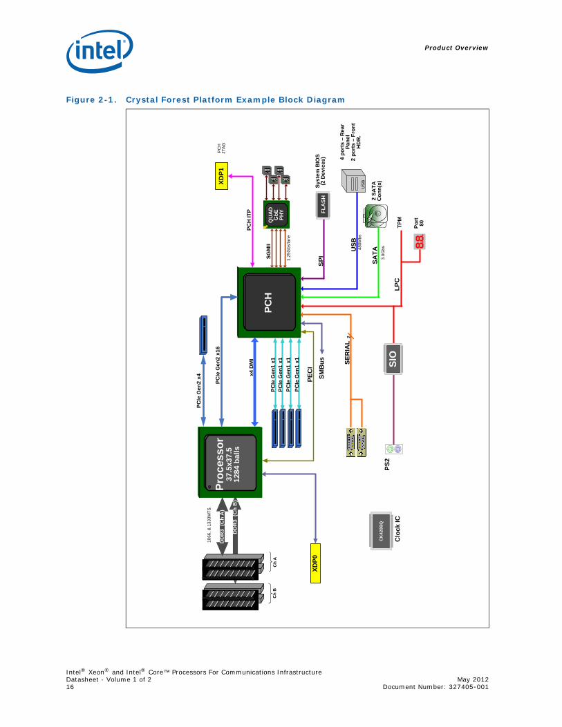
The Intel® Xeon® and Intel® Core™ Processors for Communications Infrastructure is a repackaging of the 2nd Generation Intel® Core™ Mobile Processor family. This document addresses pairing the Intel® Xeon®, Intel® Core™, Intel® Pentium®, and Intel® Celeron® processors with an Intel® Platform Controller Hub (known as the PCH), which is referred to as the Crystal Forest Platform. This platform was developed to provide flexible design options, powerful processor performance, and acceleration services that include Intel® QuickAssist Technology. Figure 2-1 shows a block diagram of the Crystal Forest Platform.
Note: The Intel® Xeon®, Intel® Core™, Intel® Pentium®, and Intel® Celeron® processors for this platform are referred to in this document as “the processor”. See Chapter 5.0 for a list of processor SKUs.
The processor is offered in either a Quad Core, Dual Core or Single Core 1284-ball FC-BGA (Flip Chip Ball Grid Array) package. All of the processor offerings are fully pin-compatible and provided in the same 37.5 x 37.5 mm FCBGA package size with a ball pitch of 1.016 mm. The processor is a 64-bit, multi-core processor built on 32-nanometer process technology. It supports DDR3 with Error Correction Code (ECC) and up to 20 PCI Express* lanes. The processor is based on the Intel® micro-architecture, formerly code named Sandy Bridge, and is designed for a two-chip platform.
Included in the processor is an integrated memory controller (IMC) and integrated I/O (PCI Express* and DMI) on a single silicon die. This single die solution is known as a monolithic processor. The integration of the memory and PCI Express* controllers into the processor silicon will benefit I/O intensive applications in the communications segments.
Note: The Intel® Xeon®, Intel® Core™, Intel® Pentium®, and Intel® Celeron® processors for this platform do not include the Integrated Display Engine or the Graphics Processor Unit (GPU). Disregard references to graphics and Intel® Turbo Boost in the 2nd Generation Intel® Core™ Processor Family Mobile Datasheet – Volume 2.
Product Overview
Intel® Xeon® and Intel® Core™ Processors For Communications InfrastructureDatasheet - Volume 1 of 2 May 201216 Document Number: 327405-001
Figure 2-1. Crystal Forest Platform Example Block Diagram
x4
DM
I
DD
R3
(C
h B
)
DD
R3
(C
h A
)
Ch
AC
h B
LP
C
SA
TAU
SB
Sys
tem
BIO
S(2
De
vic
es)
SP
I
SE
RIA
L
US
B
Po
rt
80
GbE
GbE
GbE
GbE
QU
AD
Gb
EP
HY
PC
Ie G
en
1 x
1
DR
AM
CK
420
BQ
PC
HS
GM
II
2
FL
AS
H
DR
AM
SIO
PS
2
PC
Ie G
en
1 x
1
PC
Ie G
en
1 x
1
PC
Ie G
en
1 x
1
TP
M
4 p
ort
s –
Re
ar
Pa
ne
l2
po
rts
–F
ron
t H
DR
.
2 S
AT
A
Co
nn
(s)
XD
P0
XD
P1
Clo
ck
IC
10
66, &
13
33M
TS
.
PC
H
JTA
G
PC
H I
TP
1.2
5G
bs/
lan
e
3.0
Gbs48
0Mbs
Pro
ces
so
r37
.5x
37.5
128
4b
alls
SM
Bu
s
PE
CI
PC
Ie G
en2
x1
6
PC
Ie G
en
2 x
4
FL
AS
H
Product Overview
Intel® Xeon® and Intel® Core™ Processors For Communications InfrastructureMay 2012 Datasheet - Volume 1 of 2Document Number: 327405-001 17
2.1 Product Features
2.2 Processor Details• Four, two or single execution cores (4C, 2C or 1C respectively)• 32-KB data first-level cache (L1) for each core, parity protected• 32-KB instruction first-level cache (L1) for each core, ECC protected• 256-KB shared instruction/data second-level cache (L2) for each core, ECC
protected• Up to 8-MB shared instruction/data third-level cache (L3) across all cores, ECC
protected
2.3 Supported Technologies • Intel® Virtualization Technology for Directed I/O (Intel® VT-d)• Intel® Virtualization Technology (Intel® VT-x)• Intel® Streaming SIMD Extensions 4.1 (Intel® SSE4.1)• Intel® Streaming SIMD Extensions 4.2 (Intel® SSE4.2)• Intel® Hyper-Threading Technology• Intel® 64 Architecture• Execute Disable Bit• Intel® Advanced Vector Extensions (Intel® AVX)• Advanced Encryption Standard New Instructions (AES-NI)• PCLMULQDQ Instruction
2.4 Interface Features
2.4.1 System Memory Support
• One or two channels of DDR3 memory with a maximum of two UDIMMs or two SO-DIMMs per channel
• ECC Memory Down topology of up to eighteen x8 SDRAM Devices per channel• Non-ECC Memory Down topology of up to eight x16 DDR3 SDRAM Devices per
channel• Single- and dual-channel memory organization modes• Memory capacity supported from 512 MB up to 32 GB• Using 4-Gb device technologies, the largest total memory capacity possible is 32
GB, assuming Dual Channel Mode with four x8, double-sided, dual ranked unbuffered DIMM memory configuration
• 1-Gb, 2-Gb and 4-Gb DDR3 DRAM technologies are supported for x8 and x16 devices— Using 4Gb device technology, the largest memory capacity possible is 16 GB,
assuming dual-channel mode with two x8, dual-ranked, un-buffered, DIMM memory configuration.
• Data burst length of eight for all memory organization modes• Memory DDR3 data transfer rates of 1066 MT/s, 1333 MT/s and 1600 MT/s
Product Overview
Intel® Xeon® and Intel® Core™ Processors For Communications InfrastructureDatasheet - Volume 1 of 2 May 201218 Document Number: 327405-001
• 72-bit wide channels, 64-bit data + 8-bit ECC• 64-bit wide channels, without ECC option• DDR3 I/O Voltage of 1.5 V• Supports ECC and non-ECC, unbuffered DDR3 DIMMs
— Mixing of ECC and Non-ECC DIMMS is not supported• Theoretical maximum memory bandwidth of:
— 17.1 GB/s in dual-channel mode assuming DDR3 1066 MT/s— 21.3 GB/s in dual-channel mode assuming DDR3 1333 MT/s— 25.6 GB/s in dual-channel mode assuming DDR3 1600 MT/s
• Up to 64 simultaneous open pages, 32 per channel (assuming 8 ranks of 8 bank devices)
• Memory organizations:— Single-channel modes— Dual-channel modes - Intel® Flex Memory Technology:
Dual-channel symmetric (Interleaved)• Command launch modes of 1n/2n• On-Die Termination (ODT)• Intel® Fast Memory Access (Intel® FMA):
— Just-in-Time Command Scheduling— Command Overlap— Out-of-Order Scheduling
2.4.2 PCI Express*
The PCI Express* port(s) are fully-compliant to the PCI Express Base Specification, Rev. 2.0.
The following configurations are supported:
Configuration 1— One 16-lane PCI Express* port intended to connect Processor Root Port to PCH
End Point— One 4-lane PCI Express* port intended for I/O— Four single-lane PCI Express* ports intended for I/O via the PCH
Configuration 2— One 8-lane PCI Express* port intended to connect Processor Root Port to PCH
End Point— One 8-lane PCI Express* port intended for I/O— One 4-lane PCI Express* port intended for I/O— Four single-lane PCI Express* ports intended for I/O via the PCH
Configuration 3— One 4-lane PCI Express* port intended to connect Processor Root Port to PCH
End Point— Three 4-lane PCI Express* port intended for I/O
Product Overview
Intel® Xeon® and Intel® Core™ Processors For Communications InfrastructureMay 2012 Datasheet - Volume 1 of 2Document Number: 327405-001 19
— Four single-lane PCI Express* ports intended for I/O via the PCH• PCI Express* 1 x16 port is mapped to PCI Device 1.
— One 16-lane/Two 8-lane/One 8-lane and Two 4-lane PCI Express* port• PCI Express* 1 x4 port is mapped to PCI Device 6.• The port may negotiate down to narrower widths.
— Support for x16/x8/x4/x1 widths for a single PCI Express* mode.• 2.5 GT/s and 5.0 GT/s PCI Express* frequencies are supported.• Gen1 Raw bit-rate on the data pins of 2.5 Gb/s, resulting in a real bandwidth per
pair of 250 MB/s given the 8b/10b encoding used to transmit data across this interface. This also does not account for packet overhead and link maintenance.
• Maximum theoretical bandwidth on interface of 4 GB/s in each direction simultaneously, for an aggregate of 8 GB/s when x16 Gen 1.
• Gen2 Raw bit-rate on the data pins of 5.0 Gb/s, resulting in a real bandwidth per pair of 500 MB/s given the 8b/10b encoding used to transmit data across this interface. This also does not account for packet overhead and link maintenance.
• Maximum theoretical bandwidth on interface of 8 GB/s in each direction simultaneously, for an aggregate of 8 GB/s when x16 Gen 2.
• Hierarchical PCI-compliant configuration mechanism for downstream devices.• Traditional PCI style traffic (asynchronous snooped, PCI ordering).• PCI Express* extended configuration space. The first 256 bytes of configuration
space aliases directly to the PCI Compatibility configuration space. The remaining portion of the fixed 4-KB block of memory-mapped space above that (starting at 100h) is known as extended configuration space.
• PCI Express* Enhanced Access Mechanism. Accessing the device configuration space in a flat memory mapped fashion.
• Automatic discovery, negotiation, and training of link out of reset.• Traditional AGP style traffic (asynchronous non-snooped, PCI-X Relaxed ordering).• Peer segment destination posted write traffic (no peer-to-peer read traffic) in
Virtual Channel 0:— DMI -> PCI Express* Port 1— DMI -> PCI Express* Port 2— PCI Express* Port 1 -> DMI— PCI Express* Port 2 -> DMI
• 64-bit downstream address format, but the processor never generates an address above 64 GB (Bits 63:36 will always be zeros).
• 64-bit upstream address format, but the processor responds to upstream read transactions to addresses above 64 GB (addresses where any of Bits 63:36 are nonzero) with an Unsupported Request response. Upstream write transactions to addresses above 64 GB will be dropped.
• Re-issues configuration cycles that have been previously completed with the Configuration Retry status.
• PCI Express* reference clock is 100-MHz differential clock.• Power Management Event (PME) functions.• Dynamic width capability• Message Signaled Interrupt (MSI and MSI-X) messages.• Polarity inversion.
Product Overview
Intel® Xeon® and Intel® Core™ Processors For Communications InfrastructureDatasheet - Volume 1 of 2 May 201220 Document Number: 327405-001
• Static lane numbering reversal— Does not support dynamic lane reversal, as defined (optional) by the PCI
Express Base Specification, Rev. 2.0.• Supports Half Swing “low-power/low-voltage” mode.
Note: The processor does not support PCI Express* Hot-Plug.
2.4.3 Direct Media Interface (DMI)
• DMI 2.0 support.• Four lanes in each direction.• 2.5 GT/s and 5.0 GT/s DMI interface to PCH• Gen1 Raw bit-rate on the data pins of 2.5 GT/s, resulting in a real bandwidth per
pair of 250 MB/s given the 8b/10b encoding used to transmit data across this interface. Does not account for packet overhead and link maintenance.
• Gen2 Raw bit-rate on the data pins of 5.0 GT/s, resulting in a real bandwidth per pair of 500 MB/s given the 8b/10b encoding used to transmit data across this interface. Does not account for packet overhead and link maintenance.
• Maximum theoretical bandwidth on interface of 2 GB/s in each direction simultaneously, for an aggregate of 4 GB/s when DMI x4.
• Shares 100-MHz PCI Express* reference clock.• 64-bit downstream address format, but the processor never generates an address
above 64 GB (Bits 63:36 will always be zeros).• 64-bit upstream address format, but the processor responds to upstream read
transactions to addresses above 64 GB (addresses where any of Bits 63:36 are nonzero) with an Unsupported Request response. Upstream write transactions to addresses above 64 GB will be dropped.
• Supports the following traffic types to or from the PCH:— DMI -> DRAM— DMI -> processor core (Virtual Legacy Wires (VLWs), Resetwarn, or MSIs only)— Processor core -> DMI
• APIC and MSI interrupt messaging support:— Message Signaled Interrupt (MSI and MSI-X) messages
• Downstream SMI, SCI and SERR error indication.• Legacy support for ISA regime protocol (PHOLD/PHOLDA) required for parallel port
DMA, floppy drive, and LPC bus masters.• DC coupling – no capacitors between the processor and the PCH.• Polarity inversion.• PCH end-to-end lane reversal across the link.• Supports Half Swing “low-power/low-voltage”.
2.4.4 Platform Environment Control Interface (PECI)
The PECI is a one-wire interface that provides a communication channel between a PECI client (the processor) and a PECI master. The processors support the PECI 3.0 Specification.
Product Overview
Intel® Xeon® and Intel® Core™ Processors For Communications InfrastructureMay 2012 Datasheet - Volume 1 of 2Document Number: 327405-001 21
2.5 Power Management Support
2.5.1 Processor Core
• Full support of ACPI C-states as implemented by the following processor C-states:C0, C1, C1E, C3, C6, C7
• Enhanced Intel SpeedStep® Technology
2.5.2 System
Full support of the ACPI S-states as implemented by the following system S-states:S0, S3, S4, S5
2.5.3 Memory Controller
• Conditional self-refresh (Intel® Rapid Memory Power Management (Intel® RMPM))• Dynamic power-down
2.5.4 PCI Express*
• L0s and L1 ASPM power management capability
2.5.5 DMI
• L0s and L1 ASPM power management capability
2.6 Thermal Management Support• Digital Thermal Sensor• Intel® Adaptive Thermal Monitor• THERMTRIP# and PROCHOT# support• On-Demand Mode• Memory Thermal Throttling• External Thermal Sensor (TS-on-DIMM and TS-on-Board)• Fan speed control with DTS
2.7 Package• The processor is available in one package size:
— A 37.5 x 37.5 mm 1284-ball FCBGA package (BGA1284)— 1.016 mm ball pitch
2.8 TestabilityThe processor includes boundary-scan for board and system level testability.
§ §

Product Overview
Intel® Xeon® and Intel® Core™ Processors For Communications InfrastructureDatasheet - Volume 1 of 2 May 201222 Document Number: 327405-001
Interfaces
Intel® Xeon® and Intel® Core™ Processors For Communications InfrastructureMay 2012 Datasheet - Volume 1 of 2Document Number: 327405-001 23
3.0 Interfaces
This chapter describes the interfaces supported by the processor.
3.1 System Memory Interface
3.1.1 System Memory Configurations Supported
The Integrated Memory Controller (IMC) of the processor supports DDR3 protocols with two independent, 72-bit wide channels. These two memory channels are capable of running speeds up to 1600MT/s. Each channel consists of 64 data and 8 ECC bits. In the dual-channel configuration, it supports DIMMs on both channels, or DIMMs on one channel and memory down configuration on the other channel, or memory down configuration on both channels. The processor supports up to two DIMMs per channel.
Note: Very Low Profile (VLP) UDIMMs are supported wherever UDIMMs are supported. However, VLP UDIMMs have not been fully validated.
Note: Mixing of ECC and Non-ECC DIMMs is not supported.
Interfaces
Intel® Xeon® and Intel® Core™ Processors For Communications InfrastructureDatasheet - Volume 1 of 2 May 201224 Document Number: 327405-001
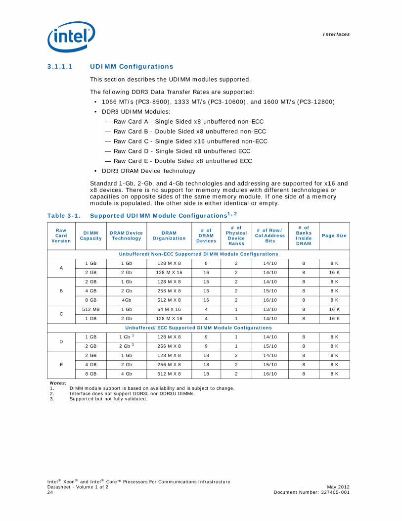
3.1.1.1 UDIMM Configurations
This section describes the UDIMM modules supported.
The following DDR3 Data Transfer Rates are supported:• 1066 MT/s (PC3-8500), 1333 MT/s (PC3-10600), and 1600 MT/s (PC3-12800)• DDR3 UDIMM Modules:
— Raw Card A - Single Sided x8 unbuffered non-ECC— Raw Card B - Double Sided x8 unbuffered non-ECC— Raw Card C - Single Sided x16 unbuffered non-ECC— Raw Card D - Single Sided x8 unbuffered ECC— Raw Card E - Double Sided x8 unbuffered ECC
• DDR3 DRAM Device Technology
Standard 1-Gb, 2-Gb, and 4-Gb technologies and addressing are supported for x16 and x8 devices. There is no support for memory modules with different technologies or capacities on opposite sides of the same memory module. If one side of a memory module is populated, the other side is either identical or empty.
Table 3-1. Supported UDIMM Module Configurations1, 2
Raw Card
Version
DIMM Capacity
DRAM Device Technology
DRAM Organization
# of DRAM
Devices
# of Physical Device Ranks
# of Row/Col Address
Bits
# of Banks Inside DRAM
Page Size
Unbuffered/Non-ECC Supported DIMM Module Configurations
A1 GB 1 Gb 128 M X 8 8 2 14/10 8 8 K
2 GB 2 Gb 128 M X 16 16 2 14/10 8 16 K
B
2 GB 1 Gb 128 M X 8 16 2 14/10 8 8 K
4 GB 2 Gb 256 M X 8 16 2 15/10 8 8 K
8 GB 4Gb 512 M X 8 16 2 16/10 8 8 K
C512 MB 1 Gb 64 M X 16 4 1 13/10 8 16 K
1 GB 2 Gb 128 M X 16 4 1 14/10 8 16 K
Unbuffered/ECC Supported DIMM Module Configurations
D1 GB 1 Gb 3 128 M X 8 9 1 14/10 8 8 K
2 GB 2 Gb 3 256 M X 8 9 1 15/10 8 8 K
E
2 GB 1 Gb 128 M X 8 18 2 14/10 8 8 K
4 GB 2 Gb 256 M X 8 18 2 15/10 8 8 K
8 GB 4 Gb 512 M X 8 18 2 16/10 8 8 K
Notes:1. DIMM module support is based on availability and is subject to change.2. Interface does not support DDR3L nor DDR3U DIMMs.3. Supported but not fully validated.
Interfaces
Intel® Xeon® and Intel® Core™ Processors For Communications InfrastructureMay 2012 Datasheet - Volume 1 of 2Document Number: 327405-001 25
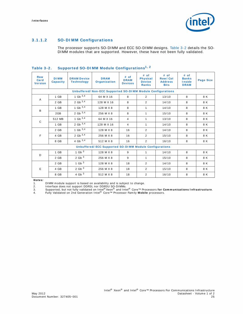
3.1.1.2 SO-DIMM Configurations
The processor supports SO-DIMM and ECC SO-DIMM designs. Table 3-2 details the SO-DIMM modules that are supported. However, these have not been fully validated.
Table 3-2. Supported SO-DIMM Module Configurations1, 2
Raw Card
Version
DIMM Capacity
DRAM Device Technology
DRAM Organization
# of DRAM
Devices
# of Physical Device Ranks
# of Row/Col Address
Bits
# of Banks Inside DRAM
Page Size
Unbuffered/Non-ECC Supported SO-DIMM Module Configurations
A1 GB 1 Gb 3,4 64 M X 16 8 2 13/10 8 8 K
2 GB 2 Gb 3,4 128 M X 16 8 2 14/10 8 8 K
B1 GB 1 Gb 3,4 128 M X 8 8 1 14/10 8 8 K
2GB 2 Gb 3,4 256 M X 8 8 1 15/10 8 8 K
C512 MB 1 Gb 3,4 64 M X 16 4 1 13/10 8 8 K
1 GB 2 Gb 3,4 128 M X 16 4 1 14/10 8 8 K
F
2 GB 1 Gb 3,4 128 M X 8 16 2 14/10 8 8 K
4 GB 2 Gb 3,4 256 M X 8 16 2 15/10 8 8 K
8 GB 4 Gb 3,4 512 M X 8 16 2 16/10 8 8 K
Unbuffered/ECC Supported SO-DIMM Module Configurations
D1 GB 1 Gb 3 128 M X 8 9 1 14/10 8 8 K
2 GB 2 Gb 3 256 M X 8 9 1 15/10 8 8 K
E
2 GB 1 Gb 3 128 M X 8 18 2 14/10 8 8 K
4 GB 2 Gb 3 256 M X 8 18 2 15/10 8 8 K
8 GB 4 Gb 3 512 M X 8 18 2 16/10 8 8 K
Notes:1. DIMM module support is based on availability and is subject to change.2. Interface does not support DDR3L nor DDR3U SO-DIMMs.3. Supported, but not fully validated on Intel®Xeon® and Intel® Core™ Processors for Communications Infrastructure.4. Fully Validated on 2nd Generation Intel® Core™ Processor Family Mobile processors.
Interfaces
Intel® Xeon® and Intel® Core™ Processors For Communications InfrastructureDatasheet - Volume 1 of 2 May 201226 Document Number: 327405-001
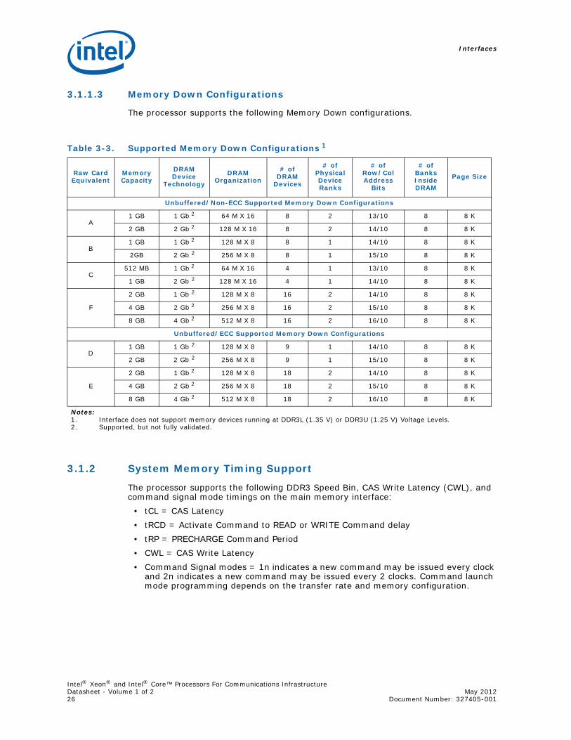
3.1.1.3 Memory Down Configurations
The processor supports the following Memory Down configurations.
3.1.2 System Memory Timing Support
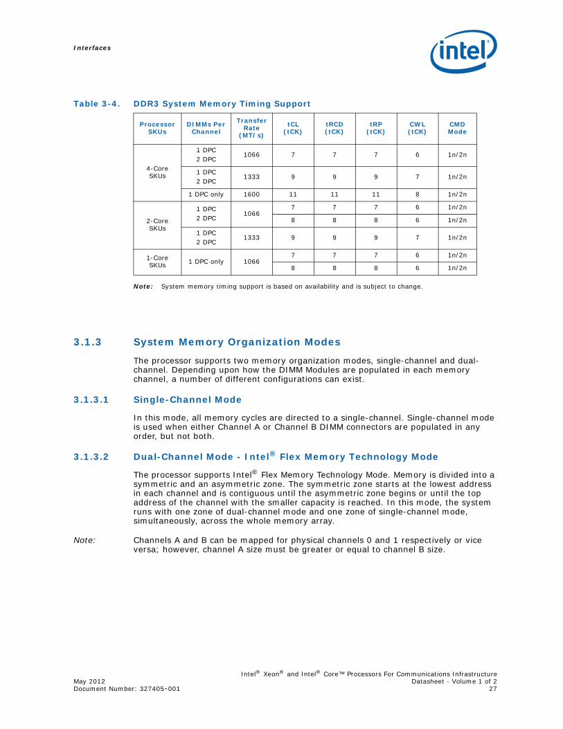
The processor supports the following DDR3 Speed Bin, CAS Write Latency (CWL), and command signal mode timings on the main memory interface:
• tCL = CAS Latency• tRCD = Activate Command to READ or WRITE Command delay• tRP = PRECHARGE Command Period• CWL = CAS Write Latency• Command Signal modes = 1n indicates a new command may be issued every clock
and 2n indicates a new command may be issued every 2 clocks. Command launch mode programming depends on the transfer rate and memory configuration.
Table 3-3. Supported Memory Down Configurations 1
Raw Card Equivalent
Memory Capacity
DRAM Device
Technology
DRAM Organization
# of DRAM
Devices
# of Physical Device Ranks
# of Row/Col Address
Bits
# of Banks Inside DRAM
Page Size
Unbuffered/Non-ECC Supported Memory Down Configurations
A1 GB 1 Gb 2 64 M X 16 8 2 13/10 8 8 K
2 GB 2 Gb 2 128 M X 16 8 2 14/10 8 8 K
B1 GB 1 Gb 2 128 M X 8 8 1 14/10 8 8 K
2GB 2 Gb 2 256 M X 8 8 1 15/10 8 8 K
C512 MB 1 Gb 2 64 M X 16 4 1 13/10 8 8 K
1 GB 2 Gb 2 128 M X 16 4 1 14/10 8 8 K
F
2 GB 1 Gb 2 128 M X 8 16 2 14/10 8 8 K
4 GB 2 Gb 2 256 M X 8 16 2 15/10 8 8 K
8 GB 4 Gb 2 512 M X 8 16 2 16/10 8 8 K
Unbuffered/ECC Supported Memory Down Configurations
D1 GB 1 Gb 2 128 M X 8 9 1 14/10 8 8 K
2 GB 2 Gb 2 256 M X 8 9 1 15/10 8 8 K
E
2 GB 1 Gb 2 128 M X 8 18 2 14/10 8 8 K
4 GB 2 Gb 2 256 M X 8 18 2 15/10 8 8 K
8 GB 4 Gb 2 512 M X 8 18 2 16/10 8 8 K
Notes:1. Interface does not support memory devices running at DDR3L (1.35 V) or DDR3U (1.25 V) Voltage Levels.2. Supported, but not fully validated.
Interfaces
Intel® Xeon® and Intel® Core™ Processors For Communications InfrastructureMay 2012 Datasheet - Volume 1 of 2Document Number: 327405-001 27
Note: System memory timing support is based on availability and is subject to change.
3.1.3 System Memory Organization Modes
The processor supports two memory organization modes, single-channel and dual-channel. Depending upon how the DIMM Modules are populated in each memory channel, a number of different configurations can exist.
3.1.3.1 Single-Channel Mode
In this mode, all memory cycles are directed to a single-channel. Single-channel mode is used when either Channel A or Channel B DIMM connectors are populated in any order, but not both.
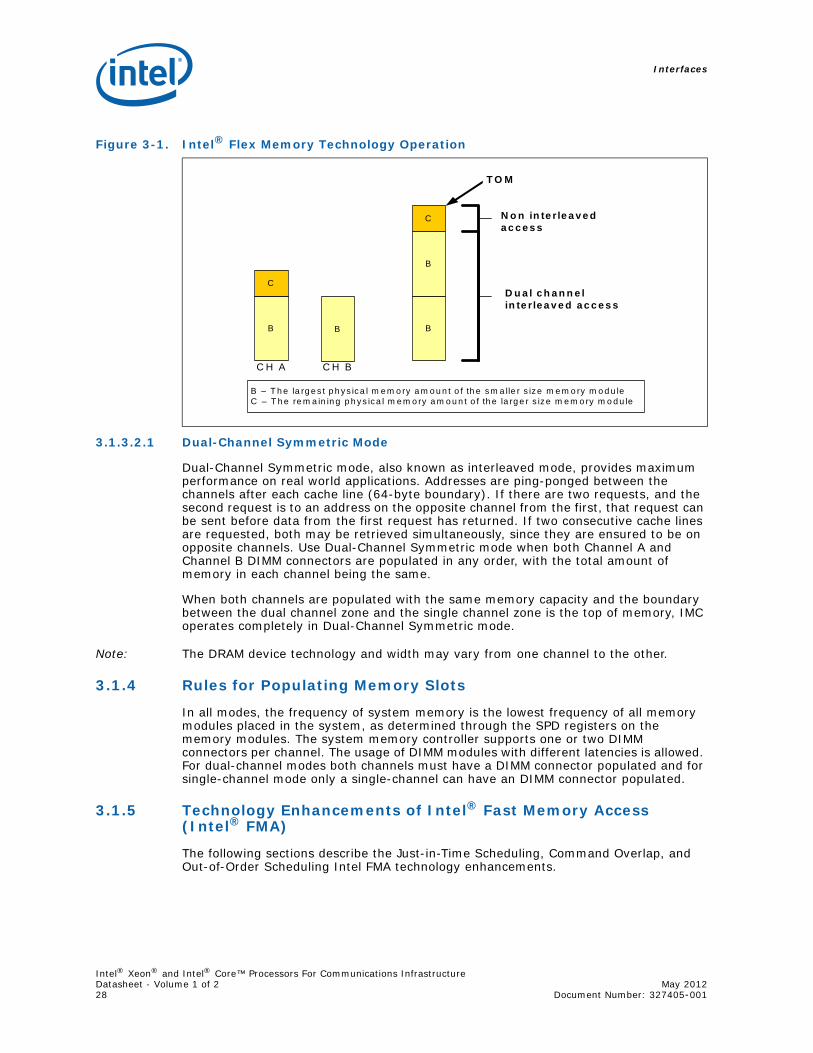
3.1.3.2 Dual-Channel Mode - Intel® Flex Memory Technology Mode
The processor supports Intel® Flex Memory Technology Mode. Memory is divided into a symmetric and an asymmetric zone. The symmetric zone starts at the lowest address in each channel and is contiguous until the asymmetric zone begins or until the top address of the channel with the smaller capacity is reached. In this mode, the system runs with one zone of dual-channel mode and one zone of single-channel mode, simultaneously, across the whole memory array.
Note: Channels A and B can be mapped for physical channels 0 and 1 respectively or vice versa; however, channel A size must be greater or equal to channel B size.
Table 3-4. DDR3 System Memory Timing Support
Processor SKUs
DIMMs Per Channel
Transfer Rate
(MT/s)
tCL (tCK)
tRCD (tCK)
tRP(tCK)
CWL (tCK)
CMDMode
4-Core SKUs
1 DPC2 DPC
1066 7 7 7 6 1n/2n
1 DPC2 DPC
1333 9 9 9 7 1n/2n
1 DPC only 1600 11 11 11 8 1n/2n
2-Core SKUs
1 DPC2 DPC
10667 7 7 6 1n/2n
8 8 8 6 1n/2n
1 DPC2 DPC
1333 9 9 9 7 1n/2n
1-Core SKUs 1 DPC only 1066
7 7 7 6 1n/2n
8 8 8 6 1n/2n
Interfaces
Intel® Xeon® and Intel® Core™ Processors For Communications InfrastructureDatasheet - Volume 1 of 2 May 201228 Document Number: 327405-001
3.1.3.2.1 Dual-Channel Symmetric Mode
Dual-Channel Symmetric mode, also known as interleaved mode, provides maximum performance on real world applications. Addresses are ping-ponged between the channels after each cache line (64-byte boundary). If there are two requests, and the second request is to an address on the opposite channel from the first, that request can be sent before data from the first request has returned. If two consecutive cache lines are requested, both may be retrieved simultaneously, since they are ensured to be on opposite channels. Use Dual-Channel Symmetric mode when both Channel A and Channel B DIMM connectors are populated in any order, with the total amount of memory in each channel being the same.
When both channels are populated with the same memory capacity and the boundary between the dual channel zone and the single channel zone is the top of memory, IMC operates completely in Dual-Channel Symmetric mode.
Note: The DRAM device technology and width may vary from one channel to the other.
3.1.4 Rules for Populating Memory Slots
In all modes, the frequency of system memory is the lowest frequency of all memory modules placed in the system, as determined through the SPD registers on the memory modules. The system memory controller supports one or two DIMM connectors per channel. The usage of DIMM modules with different latencies is allowed. For dual-channel modes both channels must have a DIMM connector populated and for single-channel mode only a single-channel can have an DIMM connector populated.
3.1.5 Technology Enhancements of Intel® Fast Memory Access (Intel® FMA)
The following sections describe the Just-in-Time Scheduling, Command Overlap, and Out-of-Order Scheduling Intel FMA technology enhancements.
Figure 3-1. Intel® Flex Memory Technology Operation
C H BC H A
B B
C
B
B
C N o n in te r le a v e d a c c e s s
D u a l c h a n n e l in te r le a v e d a c c e s s
T O M
B – T h e la rg e s t p h ys ica l m e m o ry a m o u n t o f th e sm a lle r s ize m e m o ry m o d u leC – T h e re m a in in g p h ys ica l m e m o ry a m o u n t o f th e la rg e r s ize m e m o ry m o d u le
Interfaces
Intel® Xeon® and Intel® Core™ Processors For Communications InfrastructureMay 2012 Datasheet - Volume 1 of 2Document Number: 327405-001 29
3.1.5.1 Just-in-Time Command Scheduling
The memory controller has an advanced command scheduler where all pending requests are examined simultaneously to determine the most efficient request to be issued next. The most efficient request is picked from all pending requests and issued to system memory Just-in-Time to make optimal use of Command Overlapping. Thus, instead of having all memory access requests go individually through an arbitration mechanism forcing requests to be executed one at a time, they can be started without interfering with the current request allowing for concurrent issuing of requests. This allows for optimized bandwidth and reduced latency while maintaining appropriate command spacing to meet system memory protocol.
3.1.5.2 Command Overlap
Command Overlap allows the insertion of the DRAM commands between the Activate, Precharge, and Read/Write commands normally used, as long as the inserted commands do not affect the currently executing command. Multiple commands can be issued in an overlapping manner, increasing the efficiency of system memory protocol.
3.1.5.3 Out-of-Order Scheduling
While leveraging the Just-in-Time Scheduling and Command Overlap enhancements, the IMC continuously monitors pending requests to system memory for the best use of bandwidth and reduction of latency. If there are multiple requests to the same open page, these requests would be launched in a back to back manner to make optimum use of the open memory page. This ability to reorder requests on the fly allows the IMC to further reduce latency and increase bandwidth efficiency.
3.1.5.4 Memory Type Range Registers (MTRRs) Enhancement
In this processor there are additional 2 MTRRs (total 10 MTRRs). These additional MTRRs are specially important in supporting larger system memory beyond 4GB.
3.1.6 Data Scrambling
The memory controller incorporates a DDR3 Data Scrambling feature to minimize the impact of excessive di/dt on the platform DDR3 VRs due to successive 1's and 0's on the data bus. Past experience has demonstrated that traffic on the data bus is not random and can have energy concentrated at specific spectral harmonics creating high di/dt which is generally limited by data patterns that excite resonance between the package inductance and on die capacitances. As a result the memory controller uses a data scrambling feature to create pseudo-random patterns on the DDR3 data bus to reduce the impact of any excessive di/dt.
3.1.7 DRAM Clock Generation
Every supported DIMM has two differential clock pairs. There are total of four clock pairs driven directly by the processor to two DIMMs.
3.2 PCI Express* InterfaceThis section describes the PCI Express* interface capabilities of the processor. See the PCI Express Base Specification for details of PCI Express*.
The processor has a total of 20 PCI Express* lanes. These lanes are fully compliant with PCI Express Base Specification Revision 2.0. This section will discuss how these 20 PCI Express* lanes can be utilized in various configurations on the platform.
Interfaces
Intel® Xeon® and Intel® Core™ Processors For Communications InfrastructureDatasheet - Volume 1 of 2 May 201230 Document Number: 327405-001
The processor has four PCI Express* controllers that can be independently configured to either Gen 1 or Gen 2, allowing operation at both 2.5 GT/s (Giga-Transfers per second) and 5.0 GT/s data rates. These four PCIe* devices operate simultaneously which are configurable in the following combinations:
• 1 x16 PCI Express* Port with 1 x4 PCI Express Port• 2 x8 PCI Express* Ports with 1 x4 PCI Express* Port• 1 x8 PCI Express* Ports with 3 x4 PCI Express* Ports
The 1 Core SKU (see Table 5-1, “Base Features by SKU”) only supports 16 PCI Express* Ports, and a maximum of three PCIe* devices. These three PCIe* devices operate simultaneously which are configurable in the following combinations:
• 1 x16 PCI Express* Port • 2 x8 PCI Express* Ports • 1 x8 PCI Express* Port with 2 x4 PCI Express* Ports• 3 x4 PCI Express* Ports
3.2.1 PCI Express* Architecture
Compatibility with the PCI addressing model is maintained to ensure that all existing applications and drivers operate unchanged.
The PCI Express* configuration uses standard mechanisms as defined in the PCI Plug-and-Play specification. The initial recovered clock speed of 1.25 GHz results in 2.5 Gb/s/direction which provides a 250 MB/s communications channel in each direction (500 MB/s total). That is nearly twice the data rate of classic PCI. The fact that 8b/10b encoding is used accounts for the 250 MB/s where quick calculations would imply 300 MB/s. The external ports support Gen2 speed as well. At 5.0 GT/s, Gen 2 operation results in double the bandwidth per lane as compared to Gen 1 operation. When operating with two PCIe* controllers, each controller can be operating at either 2.5 GT/s or 5.0 GT/s.
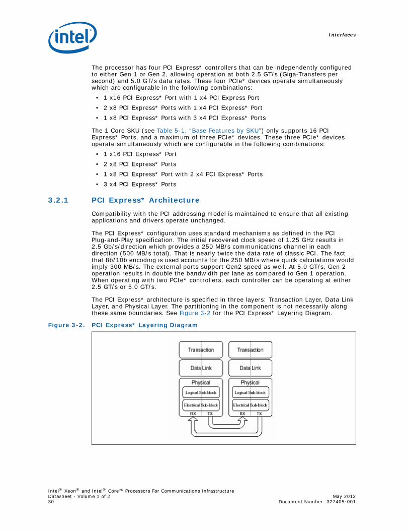
The PCI Express* architecture is specified in three layers: Transaction Layer, Data Link Layer, and Physical Layer. The partitioning in the component is not necessarily along these same boundaries. See Figure 3-2 for the PCI Express* Layering Diagram.
Figure 3-2. PCI Express* Layering Diagram
Interfaces
Intel® Xeon® and Intel® Core™ Processors For Communications InfrastructureMay 2012 Datasheet - Volume 1 of 2Document Number: 327405-001 31
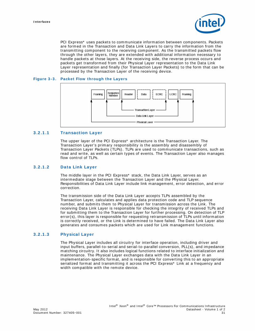
PCI Express* uses packets to communicate information between components. Packets are formed in the Transaction and Data Link Layers to carry the information from the transmitting component to the receiving component. As the transmitted packets flow through the other layers, they are extended with additional information necessary to handle packets at those layers. At the receiving side, the reverse process occurs and packets get transformed from their Physical Layer representation to the Data Link Layer representation and finally (for Transaction Layer Packets) to the form that can be processed by the Transaction Layer of the receiving device.
3.2.1.1 Transaction Layer
The upper layer of the PCI Express* architecture is the Transaction Layer. The Transaction Layer's primary responsibility is the assembly and disassembly of Transaction Layer Packets (TLPs). TLPs are used to communicate transactions, such as read and write, as well as certain types of events. The Transaction Layer also manages flow control of TLPs.
3.2.1.2 Data Link Layer
The middle layer in the PCI Express* stack, the Data Link Layer, serves as an intermediate stage between the Transaction Layer and the Physical Layer. Responsibilities of Data Link Layer include link management, error detection, and error correction.
The transmission side of the Data Link Layer accepts TLPs assembled by the Transaction Layer, calculates and applies data protection code and TLP sequence number, and submits them to Physical Layer for transmission across the Link. The receiving Data Link Layer is responsible for checking the integrity of received TLPs and for submitting them to the Transaction Layer for further processing. On detection of TLP error(s), this layer is responsible for requesting retransmission of TLPs until information is correctly received, or the Link is determined to have failed. The Data Link Layer also generates and consumes packets which are used for Link management functions.
3.2.1.3 Physical Layer
The Physical Layer includes all circuitry for interface operation, including driver and input buffers, parallel-to-serial and serial-to-parallel conversion, PLL(s), and impedance matching circuitry. It also includes logical functions related to interface initialization and maintenance. The Physical Layer exchanges data with the Data Link Layer in an implementation-specific format, and is responsible for converting this to an appropriate serialized format and transmitting it across the PCI Express* Link at a frequency and width compatible with the remote device.
Figure 3-3. Packet Flow through the Layers
Interfaces
Intel® Xeon® and Intel® Core™ Processors For Communications InfrastructureDatasheet - Volume 1 of 2 May 201232 Document Number: 327405-001
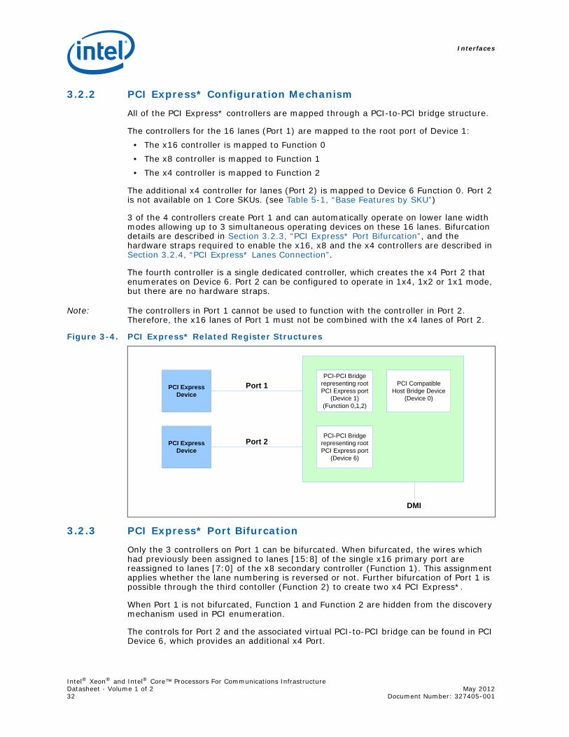
3.2.2 PCI Express* Configuration Mechanism
All of the PCI Express* controllers are mapped through a PCI-to-PCI bridge structure.
The controllers for the 16 lanes (Port 1) are mapped to the root port of Device 1:• The x16 controller is mapped to Function 0• The x8 controller is mapped to Function 1• The x4 controller is mapped to Function 2
The additional x4 controller for lanes (Port 2) is mapped to Device 6 Function 0. Port 2 is not available on 1 Core SKUs. (see Table 5-1, “Base Features by SKU”)
3 of the 4 controllers create Port 1 and can automatically operate on lower lane width modes allowing up to 3 simultaneous operating devices on these 16 lanes. Bifurcation details are described in Section 3.2.3, “PCI Express* Port Bifurcation”, and the hardware straps required to enable the x16, x8 and the x4 controllers are described in Section 3.2.4, “PCI Express* Lanes Connection”.
The fourth controller is a single dedicated controller, which creates the x4 Port 2 that enumerates on Device 6. Port 2 can be configured to operate in 1x4, 1x2 or 1x1 mode, but there are no hardware straps.
Note: The controllers in Port 1 cannot be used to function with the controller in Port 2. Therefore, the x16 lanes of Port 1 must not be combined with the x4 lanes of Port 2.
3.2.3 PCI Express* Port Bifurcation
Only the 3 controllers on Port 1 can be bifurcated. When bifurcated, the wires which had previously been assigned to lanes [15:8] of the single x16 primary port are reassigned to lanes [7:0] of the x8 secondary controller (Function 1). This assignment applies whether the lane numbering is reversed or not. Further bifurcation of Port 1 is possible through the third contoller (Function 2) to create two x4 PCI Express*.
When Port 1 is not bifurcated, Function 1 and Function 2 are hidden from the discovery mechanism used in PCI enumeration.
The controls for Port 2 and the associated virtual PCI-to-PCI bridge can be found in PCI Device 6, which provides an additional x4 Port.
Figure 3-4. PCI Express* Related Register Structures
PCI-PCI Bridge representing root PCI Express port
(Device 1)(Function 0,1,2)
PCI-PCI Bridge representing root PCI Express port
(Device 6)
PCI Compatible Host Bridge Device
(Device 0)
PCI Express Device
PCI Express Device
Port 1
Port 2
DMI
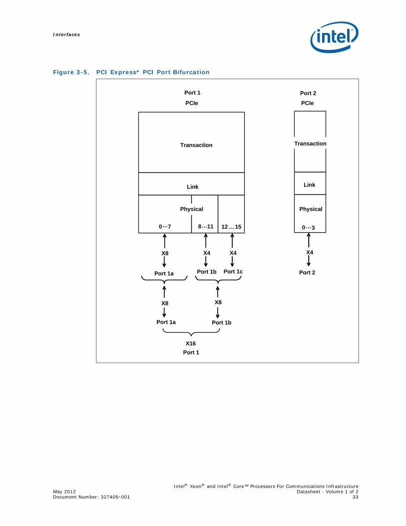
Interfaces
Intel® Xeon® and Intel® Core™ Processors For Communications InfrastructureMay 2012 Datasheet - Volume 1 of 2Document Number: 327405-001 33
Figure 3-5. PCI Express* PCI Port Bifurcation
Transaction
Link
X4X4
X8
X8
X8
4…7
Transaction
Link
8…11
Port 1
PCIe
X4
Port 1c
X4
Port 1b
X8
Port 1b
X8
Port 1a
X8
Port 1a
X16
Port 1
12 …15
X4
PCIe
X4
Port 2
Port 2
Physical Physical
LinkLink
TransactionTransaction
30…0…7
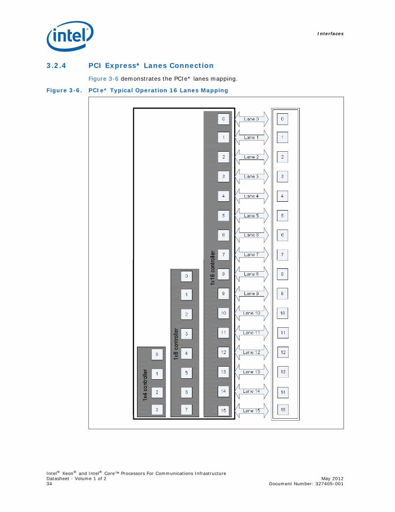
Interfaces
Intel® Xeon® and Intel® Core™ Processors For Communications InfrastructureDatasheet - Volume 1 of 2 May 201234 Document Number: 327405-001
3.2.4 PCI Express* Lanes Connection
Figure 3-6 demonstrates the PCIe* lanes mapping.
Figure 3-6. PCIe* Typical Operation 16 Lanes Mapping
Interfaces
Intel® Xeon® and Intel® Core™ Processors For Communications InfrastructureMay 2012 Datasheet - Volume 1 of 2Document Number: 327405-001 35
3.2.5 Configuring PCIe* Lanes
Note: The controllers in Port 1 cannot be used to function with the controller in Port 2. Therefore, the x16 lanes of Port 1 must not be combined with the x4 lanes of Port 2.
The following details apply to the 3 controllers in Port 1, as Port 2 cannot be bifurcated.
The configuration of the PCIe* bus is statically determined by the pre-boot software prior to initialization. The pre-boot software determines the configuration by looking at the two configuration pins, CFG[6:5], that determine whether the additional 2 controllers of the 16 lanes need to be enabled or not. These strap values are read upon power up and the pre-boot software enables the appropriate number of controllers in use as follows:
No strapping is required to enable the additional four lanes (lanes [16-19]) in any of the permissible modes as it has a single dedicated controller.
The CFG[6:5] inputs have a default value of [1:1] if they are not terminated on the board. By default, a single x16 controller is enabled. When a logic 0 is required on the strap, it is recommended that they be pulled down to ground with a 1 K Ohm resistor
Note: If the x16 controller is enabled by the hardware strapping and a x8 device is plugged in, the controller automatically operates in the x8 mode. The same is true for any controller that is connected to a device operating at narrower lane widths.
Hot plug is not supported on these PCIe* interfaces. If a device is not present at power up, it is not detected when it is plugged in after power up. Also, the strap values are read upon power up and the pre-boot software enables the appropriate controller based on the value read on CFG[6:5]. Hence, if a device of lower lane width than the width of the controller that is enabled is plugged in before power up, then it is automatically detected. But if a device with higher lane width is plugged in, the device is not detected. The same is true for the number of controllers enabled. If a single controller is enabled at power up, then a single device of any width equal to or lower than the width of the controller is detected.
For example, if upon power up, the value on CFG [6:5] is [1:1], then the 1x16 controller is enabled. A single device of width x16 will be detected upon power up. But if two devices of any lower width are plugged in; only the device connected to Device 1, Function 0 will be detected.
Table 3-5. Hardware Straps for PCIe* Controller Enabling (Port 1 Only)
CFG [6:5] Mode
00 1x8 +2x4
01 Reserved
10 2x8
11 (default) 1x16
Interfaces
Intel® Xeon® and Intel® Core™ Processors For Communications InfrastructureDatasheet - Volume 1 of 2 May 201236 Document Number: 327405-001
3.2.6 Lane Reversal on PCIe* Interface
The PCI Express* lanes can be reversed for ease of design and layout. Lane reversal is done statically, which means that the BIOS needs to configure the reversal before the relevant root port is enabled. For the x16 configuration, only one reversal option is supported allowing either a straight or a rotated CPU on the motherboard. No other combination of partial slot reversal is permitted. The reversal on x8 and x4 configurations are applied in a similar fashion.
The normal or reversed configuration is determined by the configuration pins CFG[2] for PCI express lanes on Port 1 and CFG[3] for lanes on Port 2. A value of '1' on these inputs would indicate normal operation and a '0' would indicate reversed mode of operation, as shown in Table 2.
Note: Performance estimates on early silicon have shown that bandwidth in x16 mode for Gen 2 is approximately twice the bandwidth in x8 mode for read, write and read-write transaction.
3.3 Direct Media InterfaceDirect Media Interface (DMI) connects the processor and the PCH. Next generation DMI2 is supported.
Note: Only DMI x4 configuration is supported.
3.3.1 DMI Error Flow
DMI can only generate SERR in response to errors, never SCI, SMI, MSI, PCI INT, orGPE. Any DMI related SERR activity is associated with Device 0.
3.3.2 DMI Link Down
The DMI link going down is a fatal, unrecoverable error. If the DMI data link goes to data link down, after the link was up, then the DMI link hangs the system by not allowing the link to retrain to prevent data corruption. This link behavior is controlled by the PCH.
Downstream transactions that had been successfully transmitted across the link prior to the link going down may be processed as normal. No completions from downstream, non-posted transactions are returned upstream over the DMI link after a link down event.
3.4 Platform Environment Control Interface (PECI)The PECI is a one-wire interface that provides a communication channel between a PECI client (processor) and a PECI master. The processor implements a PECI interface to:
Table 3-6. Hardware Straps for Normal/Reversed Operation of PCIe* Lanes
PCI-e Lanes Normal Reversed
Port 1 CFG [2] =1 CFG [2] =0
Port 2 CFG [3] =1 CFG [3] =0
Interfaces
Intel® Xeon® and Intel® Core™ Processors For Communications InfrastructureMay 2012 Datasheet - Volume 1 of 2Document Number: 327405-001 37
• Allow communication of processor thermal and other information to the PECI master.
• Read averaged Digital Thermal Sensor (DTS) values for fan speed control.
3.5 Interface Clocking
3.5.1 Internal Clocking Requirements
§ §
Table 3-7. Reference Clock
Reference Input Clock Input Frequency Associated PLL
BCLK/BCLK# 100 MHz Processor/Memory/PCIe/DMI
Interfaces
Intel® Xeon® and Intel® Core™ Processors For Communications InfrastructureDatasheet - Volume 1 of 2 May 201238 Document Number: 327405-001
Technologies
Intel® Xeon® and Intel® Core™ Processors For Communications InfrastructureMay 2012 Datasheet - Volume 1 of 2Document Number: 327405-001 39
4.0 Technologies
4.1 Intel® Virtualization TechnologyIntel® Virtualization Technology (Intel® VT) makes a single system appear as multiple independent systems to software. This allows multiple, independent operating systems to run simultaneously on a single system. Intel® VT comprises technology components to support virtualization of platforms based on Intel architecture microprocessors and chipsets. Intel® Virtualization Technology (Intel® VT) for IA-32, Intel® 64 and Intel® Architecture (Intel® VT-x) added hardware support in the processor to improve the virtualization performance and robustness. Intel® Virtualization Technology for Directed I/O (Intel® VT-d) adds chipset hardware implementation to support and improve I/O virtualization performance and robustness.
Intel® VT-x specifications and functional descriptions are included in the Intel® 64 and IA-32 Architectures Software Developer’s Manual, Volume 3B and is available at
http://www.intel.com/products/processor/manuals/index.htm
The Intel® VT-d spec and other VT documents can be referenced at
http://www.intel.com/technology/platform-technology/virtualization/index.htm
4.1.1 Intel® VT-x Objectives
Intel® VT-x provides hardware acceleration for virtualization of IA platforms. Virtual Machine Monitor (VMM) can use Intel® VT-x features to provide improved reliable virtualized platform. By using Intel® VT-x, a VMM is:
• Robust: VMMs no longer need to use paravirtualization or binary translation. This means that they will be able to run off-the-shelf OSs and applications without any special steps.
• Enhanced: Intel® VT enables VMMs to run 64-bit guest operating systems on IA x86 processors.
• More reliable: Due to the hardware support, VMMs can now be smaller, less complex, and more efficient. This improves reliability and availability and reduces the potential for software conflicts.
• More secure: The use of hardware transitions in the VMM strengthens the isolation of VMs and further prevents corruption of one VM from affecting others on the same system.
4.1.2 Intel® VT-x Features
The processor core supports the following Intel® VT-x features:• Extended Page Tables (EPT)
— EPT is hardware assisted page table virtualization— It eliminates VM exits from guest OS to the VMM for shadow page-table
maintenance
Technologies
Intel® Xeon® and Intel® Core™ Processors For Communications InfrastructureDatasheet - Volume 1 of 2 May 201240 Document Number: 327405-001
• Virtual Processor IDs (VPID)— Ability to assign a VM ID to tag processor core hardware structures (e.g., TLBs) — This avoids flushes on VM transitions to give a lower-cost VM transition time
and an overall reduction in virtualization overhead.• Guest Preemption Timer
— Mechanism for a VMM to preempt the execution of a guest OS after an amount of time specified by the VMM. The VMM sets a timer value before entering a guest
— The feature aids VMM developers in flexibility and Quality of Service (QoS) guarantees
• Descriptor-Table Exiting— Descriptor-table exiting allows a VMM to protect a guest OS from internal
(malicious software based) attack by preventing relocation of key system data structures like IDT (interrupt descriptor table), GDT (global descriptor table), LDT (local descriptor table), and TSS (task segment selector).
— A VMM using this feature can intercept (by a VM exit) attempts to relocate these data structures and prevent them from being tampered by malicious software.
4.1.3 Intel® VT-d Objectives
The key Intel® VT-d objectives are domain-based isolation and hardware-based virtualization. A domain can be abstractly defined as an isolated environment in a platform to which a subset of host physical memory is allocated. Virtualization allows for the creation of one or more partitions on a single system. This could be multiple partitions in the same operating system, or there can be multiple operating system instances running on the same system, offering benefits like system consolidation, legacy migration, activity partitioning, or security.
4.1.4 Intel® VT-d Features
The processor supports the following Intel® VT-d features:• Memory controller complies with Intel® VT-d 1.2 specification. • Intel® VT-d DMA remap engines.
— DMI (non-high def audio)— PCI Express*
• Support for root entry, context entry and default context• 39-bit guest physical address and host physical address widths• Support for 4K page sizes only• Support for register-based fault recording only (for single entry only) and support
for MSI interrupts for faults• Support for both leaf and non-leaf caching• Support for boot protection of default page table• Support for non-caching of invalid page table entries• Support for hardware based flushing of translated but pending writes and pending
reads, on IOTLB invalidation• Support for page-selective IOTLB invalidation
Technologies
Intel® Xeon® and Intel® Core™ Processors For Communications InfrastructureMay 2012 Datasheet - Volume 1 of 2Document Number: 327405-001 41
• MSI cycles (MemWr to address FEEx_xxxxh) not translated— Translation faults result in cycle forwarding to VBIOS region (byte enables
masked for writes). Returned data may be bogus for internal agents, PEG/DMI interfaces return unsupported request status
• Interrupt Remapping is supported• Queued invalidation is supported.• VT-d translation bypass address range is supported (Pass Through)• Support for ARI (Alternative Requester ID - a PCI SIG ECR for increasing the
function number count in a PCIe device) to support IOV devices.
4.1.5 Intel® VT-d Features Not Supported
The following features are not supported by the processor with Intel® VT-d:• No support for PCISIG endpoint caching (ATS)• No support for Intel® VT-d read prefetching/snarfing i.e. translations within a
cacheline are not stored in an internal buffer for reuse for subsequent translations.• No support for advance fault reporting• No support for super pages• No support for Intel® VT-d translation bypass address range (such usage models
need to be resolved with VMM help in setting up the page tables correctly)
4.2 Intel® Hyper-Threading TechnologyThe processor supports Intel® Hyper-Threading Technology (Intel® HT Technology), which allows an execution core to function as two logical processors. While some execution resources such as caches, execution units, and buses are shared, each logical processor has its own architectural state with its own set of general-purpose registers and control registers. This feature must be enabled via the BIOS and requires operating system support.
Intel recommends enabling Hyper-Threading Technology with Microsoft Windows 7*, Microsoft Windows Vista*, Microsoft Windows* XP Professional/Windows* XP Home, and disabling Hyper-Threading Technology via the BIOS for all previous versions of Windows operating systems. For more information on Hyper-Threading Technology, see http://www.intel.com/technology/platform-technology/hyper-threading/.
4.3 Intel® Advanced Vector Extensions (Intel® AVX)Intel® Advanced Vector Extensions (Intel® AVX) is the latest expansion of the Intel instruction set. It extends the Intel® Streaming SIMD Extensions (SSE) from 128-bit vectors into 256-bit vectors. Intel® AVX addresses the continued need for vector floating-point performance in mainstream scientific and engineering numerical applications, visual processing, recognition, data-mining/synthesis, gaming, physics, cryptography and other areas of applications. The enhancement in Intel® AVX allows for improved performance due to wider vectors, new extensible syntax, and rich functionality including the ability to better manage, rearrange, and sort data. For more information on Intel® AVX, see http://www.intel.com/software/avx.
Technologies
Intel® Xeon® and Intel® Core™ Processors For Communications InfrastructureDatasheet - Volume 1 of 2 May 201242 Document Number: 327405-001
4.4 Intel® Advanced Encryption Standard New Instructions (Intel® AES-NI)The processor supports Advanced Encryption Standard New Instructions (Intel® AES-NI), which are a set of Single Instruction Multiple Data (SIMD) instructions that enable fast and secure data encryption and decryption based on the Advanced Encryption Standard (AES). Intel® AES-NI are valuable for a wide range of cryptographic applications, for example: applications that perform bulk encryption/decryption, authentication, random number generation, and authenticated encryption. AES is broadly accepted as the standard for both government and industry applications, and is widely deployed in various protocols.
Intel® AES-NI consists of six Intel® SSE instructions. Four instructions, namely AESENC, AESENCLAST, AESDEC, and AESDELAST facilitate high performance AES encryption and decryption. The other two, namely AESIMC and AESKEYGENASSIST, support the AES key expansion procedure. Together, these instructions provide a full hardware for support AES, offering security, high performance, and a great deal of flexibility.
4.4.1 PCLMULQDQ Instruction
The processor supports the carry-less multiplication instruction, PCLMULQDQ. PCLMULQDQ is a Single Instruction Multiple Data (SIMD) instruction that computes the 128-bit carry-less multiplication of two, 64-bit operands without generating and propagating carries. Carry-less multiplication is an essential processing component of several cryptographic systems and standards. Hence, accelerating carry-less multiplication can significantly contribute to achieving high speed secure computing and communication.
4.5 Intel® 64 Architecture x2APICThe x2APIC architecture extends the xAPIC architecture which provides key mechanism for interrupt delivery. This extension is intended primarily to increase processor addressability.
Specifically, x2APIC:• Retains all key elements of compatibility to the xAPIC architecture:
— delivery modes— interrupt and processor priorities— interrupt sources— interrupt destination types
• Provides extensions to scale processor addressability for both the logical and physical destination modes.
• Adds new features to enhance performance of interrupt delivery.• Reduces complexity of logical destination mode interrupt delivery on link based
architectures.
The key enhancements provided by the x2APIC architecture over xAPIC are the following:
• Support for two modes of operation to provide backward compatibility and extensibility for future platform innovations.— In xAPIC compatibility mode, APIC registers are accessed through memory
mapped interface to a 4K-Byte page, identical to the xAPIC architecture.
Technologies
Intel® Xeon® and Intel® Core™ Processors For Communications InfrastructureMay 2012 Datasheet - Volume 1 of 2Document Number: 327405-001 43
— In x2APIC mode, APIC registers are accessed through Model Specific Register (MSR) interfaces. In this mode, the x2APIC architecture provides significantly increased processor addressability and some enhancements on interrupt delivery.
• Increased range of processor addressability in x2APIC mode:— Physical xAPIC ID field increases from 8 bits to 32 bits, allowing for interrupt
processor addressability up to 4G-1 processors in physical destination mode. A processor implementation of x2APIC architecture can support fewer than 32-bits in a software transparent fashion.
— Logical xAPIC ID field increases from 8 bits to 32 bits. The 32-bit logical x2APIC ID is partitioned into two sub-fields: a 16-bit cluster ID and a 16-bit logical ID within the cluster. Consequently, ((2^20) -16) processors can be addressed in logical destination mode. Processor implementations can support fewer than 16 bits in the cluster ID sub-field and logical ID sub-field in a software agnostic fashion.
• More efficient MSR interface to access APIC registers.— To enhance inter-processor and self directed interrupt delivery as well as the
ability to virtualize the local APIC, the APIC register set can be accessed only through MSR based interfaces in the x2APIC mode. The Memory Mapped IO (MMIO) interface used by xAPIC is not supported in the x2APIC mode.
• The semantics for accessing APIC registers have been revised to simplify the programming of frequently-used APIC registers by system software. Specifically the software semantics for using the Interrupt Command Register (ICR) and End Of Interrupt (EOI) registers have been modified to allow for more efficient delivery and dispatching of interrupts.
The x2APIC extensions are made available to system software by enabling the local x2APIC unit in the “x2APIC” mode. In order to benefit from x2APIC capabilities, a new Operating System and a new BIOS are both needed, with special support for the x2APIC mode.
The x2APIC architecture provides backward compatibility to the xAPIC architecture and forward extendibility for future Intel platform innovations.
Note: Intel x2APIC technology may not be available on all SKUs.
For more information see the Intel® 64 Architecture x2APIC specification at http://www.intel.com/products/processor/manuals/
§ §

Technologies
Intel® Xeon® and Intel® Core™ Processors For Communications InfrastructureDatasheet - Volume 1 of 2 May 201244 Document Number: 327405-001
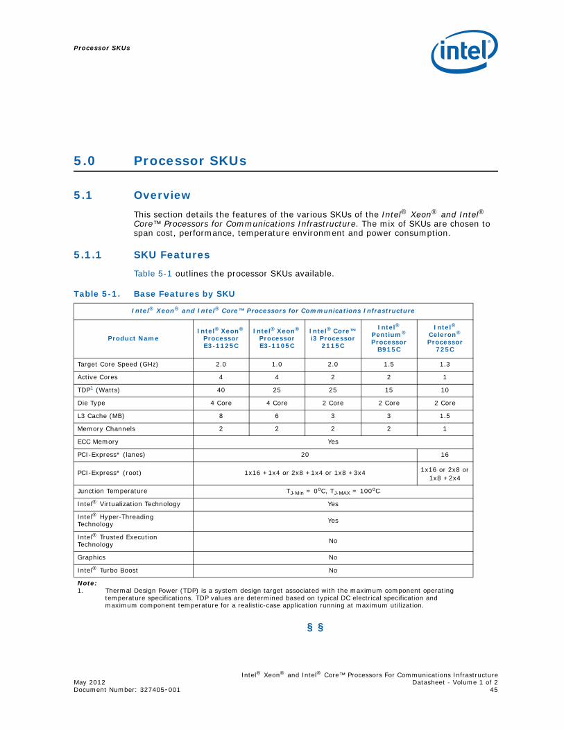
Processor SKUs
Intel® Xeon® and Intel® Core™ Processors For Communications InfrastructureMay 2012 Datasheet - Volume 1 of 2Document Number: 327405-001 45
5.0 Processor SKUs
5.1 OverviewThis section details the features of the various SKUs of the Intel® Xeon® and Intel®
Core™ Processors for Communications Infrastructure. The mix of SKUs are chosen to span cost, performance, temperature environment and power consumption.
5.1.1 SKU Features
Table 5-1 outlines the processor SKUs available.
§ §
Table 5-1. Base Features by SKU
Intel® Xeon® and Intel® Core™ Processors for Communications Infrastructure
Product NameIntel® Xeon®
Processor E3-1125C
Intel® Xeon® Processor E3-1105C
Intel® Core™ i3 Processor
2115C
Intel® Pentium® Processor
B915C
Intel® Celeron® Processor
725C
Target Core Speed (GHz) 2.0 1.0 2.0 1.5 1.3
Active Cores 4 4 2 2 1
TDP1 (Watts) 40 25 25 15 10
Die Type 4 Core 4 Core 2 Core 2 Core 2 Core
L3 Cache (MB) 8 6 3 3 1.5
Memory Channels 2 2 2 2 1
ECC Memory Yes
PCI-Express* (lanes) 20 16
PCI-Express* (root) 1x16 +1x4 or 2x8 +1x4 or 1x8 +3x4 1x16 or 2x8 or1x8 +2x4
Junction Temperature TJ-Min = 0oC, TJ-MAX = 100oC
Intel® Virtualization Technology Yes
Intel® Hyper-Threading Technology Yes
Intel® Trusted Execution Technology No
Graphics No
Intel® Turbo Boost No
Note:1. Thermal Design Power (TDP) is a system design target associated with the maximum component operating
temperature specifications. TDP values are determined based on typical DC electrical specification and maximum component temperature for a realistic-case application running at maximum utilization.

Processor SKUs
Intel® Xeon® and Intel® Core™ Processors For Communications InfrastructureDatasheet - Volume 1 of 2 May 201246 Document Number: 327405-001
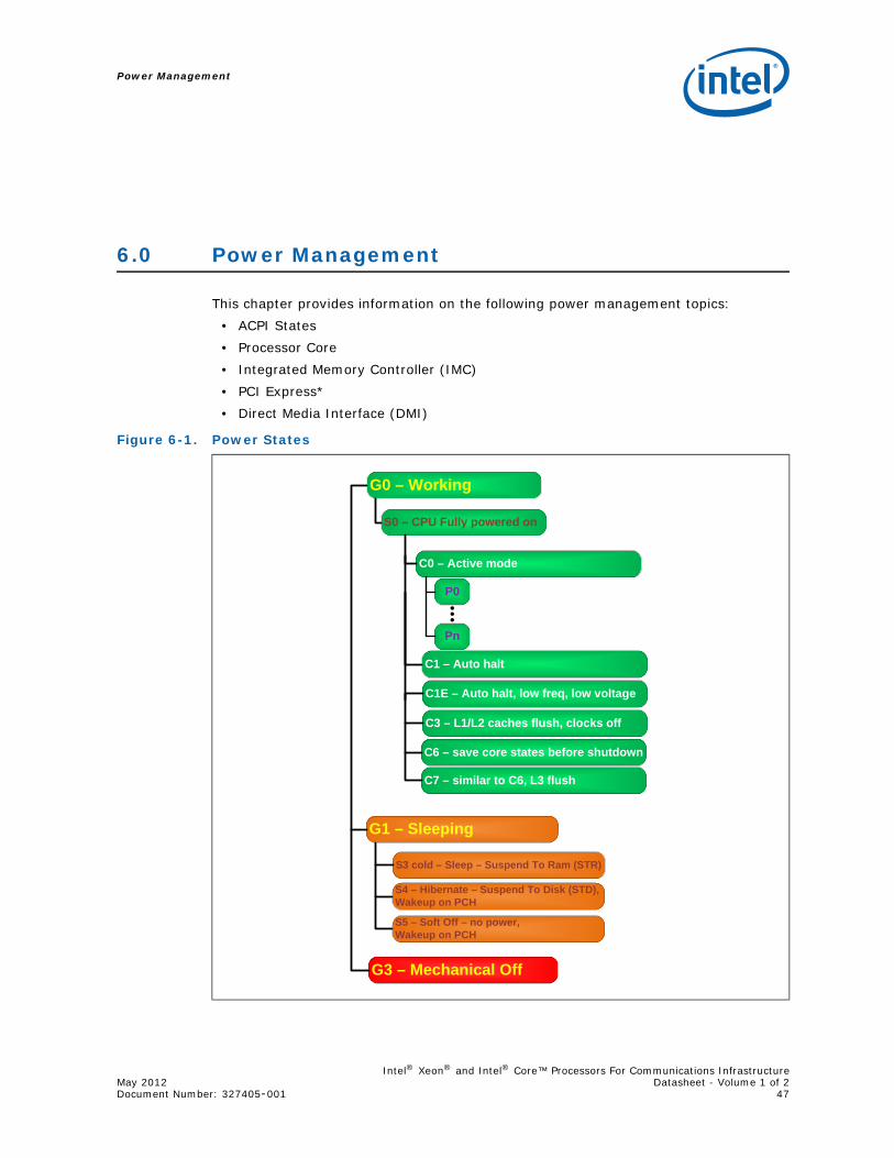
Power Management
Intel® Xeon® and Intel® Core™ Processors For Communications InfrastructureMay 2012 Datasheet - Volume 1 of 2Document Number: 327405-001 47
6.0 Power Management
This chapter provides information on the following power management topics:• ACPI States• Processor Core• Integrated Memory Controller (IMC)• PCI Express*• Direct Media Interface (DMI)
Figure 6-1. Power States
G0 – Working
S0 – CPU Fully powered on
C0 – Active mode
C1 – Auto halt
C1E – Auto halt, low freq, low voltage
C3 – L1/L2 caches flush, clocks off
C6 – save core states before shutdown
C7 – similar to C6, L3 flush
G1 – Sleeping
S3 cold – Sleep – Suspend To Ram (STR)
S4 – Hibernate – Suspend To Disk (STD), Wakeup on PCH
S5 – Soft Off – no power,Wakeup on PCH
G3 – Mechanical Off
P0
Pn
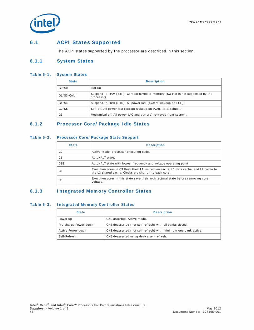
Power Management
Intel® Xeon® and Intel® Core™ Processors For Communications InfrastructureDatasheet - Volume 1 of 2 May 201248 Document Number: 327405-001
6.1 ACPI States SupportedThe ACPI states supported by the processor are described in this section.
6.1.1 System States
6.1.2 Processor Core/Package Idle States
6.1.3 Integrated Memory Controller States
Table 6-1. System States
State Description
G0/S0 Full On
G1/S3-Cold Suspend-to-RAM (STR). Context saved to memory (S3-Hot is not supported by the processor).
G1/S4 Suspend-to-Disk (STD). All power lost (except wakeup on PCH).
G2/S5 Soft off. All power lost (except wakeup on PCH). Total reboot.
G3 Mechanical off. All power (AC and battery) removed from system.
Table 6-2. Processor Core/Package State Support
State Description
C0 Active mode, processor executing code.
C1 AutoHALT state.
C1E AutoHALT state with lowest frequency and voltage operating point.
C3 Execution cores in C3 flush their L1 instruction cache, L1 data cache, and L2 cache to the L3 shared cache. Clocks are shut off to each core.
C6 Execution cores in this state save their architectural state before removing core voltage.
Table 6-3. Integrated Memory Controller States
State Description
Power up CKE asserted. Active mode.
Pre-charge Power-down CKE deasserted (not self-refresh) with all banks closed.
Active Power-down CKE deasserted (not self-refresh) with minimum one bank active.
Self-Refresh CKE deasserted using device self-refresh.
Power Management
Intel® Xeon® and Intel® Core™ Processors For Communications InfrastructureMay 2012 Datasheet - Volume 1 of 2Document Number: 327405-001 49
6.1.4 PCIe* Link States
6.1.5 DMI States
6.1.6 Interface State Combinations
6.2 Processor Core Power ManagementWhile executing code, Enhanced Intel SpeedStep® Technology optimizes the processor’s frequency and core voltage based on workload. Each frequency and voltage operating point is defined by ACPI as a P-state. When the processor is not executing code, it is idle. A low-power idle state is defined by ACPI as a C-state. In general, lower power C-states have longer entry and exit latencies.
Table 6-4. PCIe* Link States
State Description
L0 Full on – Active transfer state.
L0s First Active Power Management low power state – Low exit latency.
L1 Lowest Active Power Management - Longer exit latency.
L3 Lowest power state (power-off) – Longest exit latency.
Table 6-5. DMI States
State Description
L0 Full on – Active transfer state.
L0s First Active Power Management low power state – Low exit latency.
L1 Lowest Active Power Management - Longer exit latency.
L3 Lowest power state (power-off) – Longest exit latency.
Table 6-6. G, S and C State Combinations
Global (G) State
Sleep (S) State
Processor Core
(C) State
Processor State System Clocks Description
G0 S0 C0 Full On On Full On
G0 S0 C1/C1E Auto-Halt On Auto-Halt
G0 S0 C3 Deep Sleep On Deep Sleep
G0 S0 C6/C7 Deep Power-down On Deep Power Down
G1 S3 Power off Off, except RTC Suspend to RAM
G1 S4 Power off Off, except RTC Suspend to Disk
G2 S5 Power off Off, except RTC Soft Off
G3 NA Power off Power off Hard off
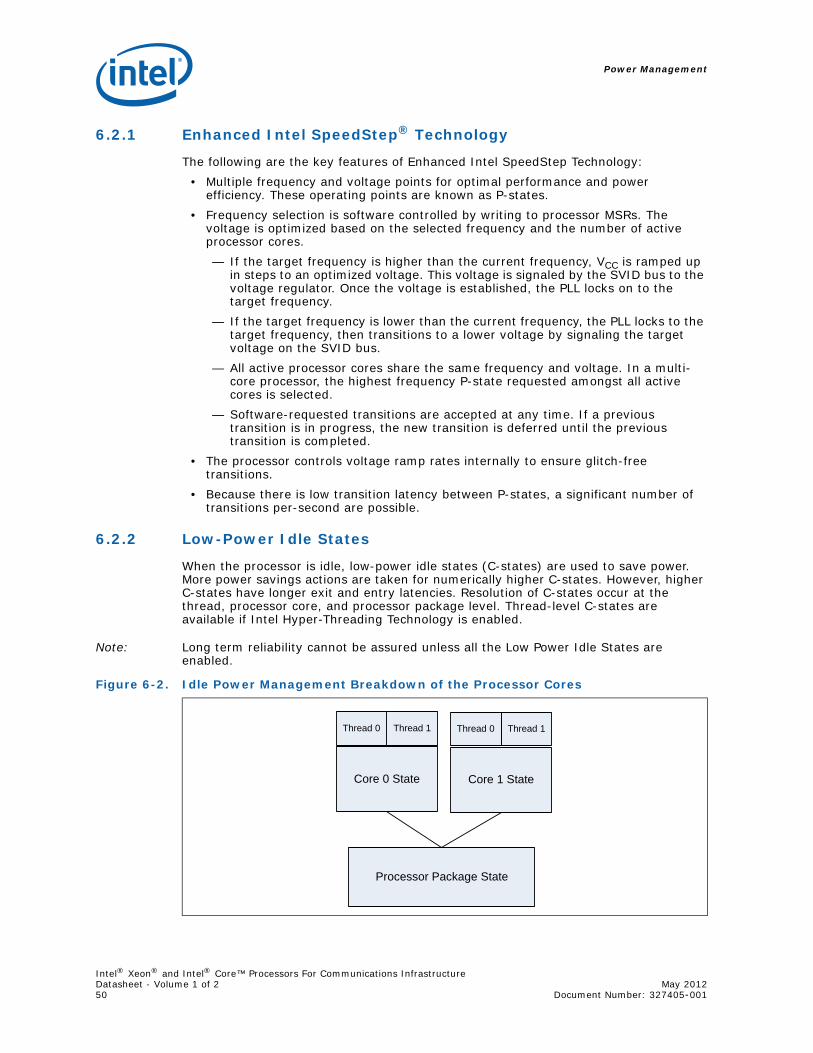
Power Management
Intel® Xeon® and Intel® Core™ Processors For Communications InfrastructureDatasheet - Volume 1 of 2 May 201250 Document Number: 327405-001
6.2.1 Enhanced Intel SpeedStep® Technology
The following are the key features of Enhanced Intel SpeedStep Technology:• Multiple frequency and voltage points for optimal performance and power
efficiency. These operating points are known as P-states.• Frequency selection is software controlled by writing to processor MSRs. The
voltage is optimized based on the selected frequency and the number of active processor cores.— If the target frequency is higher than the current frequency, VCC is ramped up
in steps to an optimized voltage. This voltage is signaled by the SVID bus to the voltage regulator. Once the voltage is established, the PLL locks on to the target frequency.
— If the target frequency is lower than the current frequency, the PLL locks to the target frequency, then transitions to a lower voltage by signaling the target voltage on the SVID bus.
— All active processor cores share the same frequency and voltage. In a multi-core processor, the highest frequency P-state requested amongst all active cores is selected.
— Software-requested transitions are accepted at any time. If a previous transition is in progress, the new transition is deferred until the previous transition is completed.
• The processor controls voltage ramp rates internally to ensure glitch-free transitions.
• Because there is low transition latency between P-states, a significant number of transitions per-second are possible.
6.2.2 Low-Power Idle States
When the processor is idle, low-power idle states (C-states) are used to save power. More power savings actions are taken for numerically higher C-states. However, higher C-states have longer exit and entry latencies. Resolution of C-states occur at the thread, processor core, and processor package level. Thread-level C-states are available if Intel Hyper-Threading Technology is enabled.
Note: Long term reliability cannot be assured unless all the Low Power Idle States are enabled.
Figure 6-2. Idle Power Management Breakdown of the Processor Cores
Processor Package State
Core 1 State
Thread 1Thread 0
Core 0 State
Thread 1Thread 0
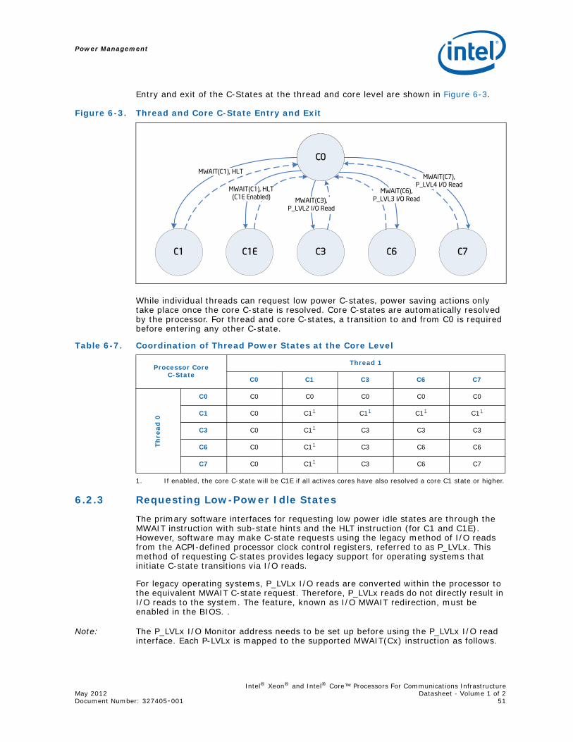
Power Management
Intel® Xeon® and Intel® Core™ Processors For Communications InfrastructureMay 2012 Datasheet - Volume 1 of 2Document Number: 327405-001 51
Entry and exit of the C-States at the thread and core level are shown in Figure 6-3.
While individual threads can request low power C-states, power saving actions only take place once the core C-state is resolved. Core C-states are automatically resolved by the processor. For thread and core C-states, a transition to and from C0 is required before entering any other C-state.
6.2.3 Requesting Low-Power Idle States
The primary software interfaces for requesting low power idle states are through the MWAIT instruction with sub-state hints and the HLT instruction (for C1 and C1E). However, software may make C-state requests using the legacy method of I/O reads from the ACPI-defined processor clock control registers, referred to as P_LVLx. This method of requesting C-states provides legacy support for operating systems that initiate C-state transitions via I/O reads.
For legacy operating systems, P_LVLx I/O reads are converted within the processor to the equivalent MWAIT C-state request. Therefore, P_LVLx reads do not directly result in I/O reads to the system. The feature, known as I/O MWAIT redirection, must be enabled in the BIOS. .
Note: The P_LVLx I/O Monitor address needs to be set up before using the P_LVLx I/O read interface. Each P-LVLx is mapped to the supported MWAIT(Cx) instruction as follows.
Figure 6-3. Thread and Core C-State Entry and Exit
C1 C1E C7C6C3
C0MWAIT(C1), HLT
C0
MWAIT(C7),P_LVL4 I/O Read
MWAIT(C6),P_LVL3 I/O ReadMWAIT(C3),
P_LVL2 I/O Read
MWAIT(C1), HLT (C1E Enabled)
Table 6-7. Coordination of Thread Power States at the Core Level
Processor Core C-State
Thread 1
C0 C1 C3 C6 C7
Thre
ad 0
C0 C0 C0 C0 C0 C0
C1 C0 C11
1. If enabled, the core C-state will be C1E if all actives cores have also resolved a core C1 state or higher.
C11 C11 C11
C3 C0 C11 C3 C3 C3
C6 C0 C11 C3 C6 C6
C7 C0 C11 C3 C6 C7
Power Management
Intel® Xeon® and Intel® Core™ Processors For Communications InfrastructureDatasheet - Volume 1 of 2 May 201252 Document Number: 327405-001
The BIOS can write to the C-state range field of the PMG_IO_CAPTURE MSR to restrict the range of I/O addresses that are trapped and emulate MWAIT like functionality. Any P_LVLx reads outside of this range does not cause an I/O redirection to MWAIT(Cx) like request. They fall through like a normal I/O instruction.
Note: When P_LVLx I/O instructions are used, MWAIT substates cannot be defined. The MWAIT substate is always zero if I/O MWAIT redirection is used. By default, P_LVLx I/O redirections enable the MWAIT 'break on EFLAGS.IF’ feature which triggers a wakeup on an interrupt even if interrupts are masked by EFLAGS.IF.
6.2.4 Core C-states
The following are general rules for all core C-states, unless specified otherwise:• A core C-State is determined by the lowest numerical thread state (e.g., Thread 0
requests C1E while Thread 1 requests C3, resulting in a core C1E state). See Table 6-6, “G, S and C State Combinations”.
• A core transitions to C0 state when:— An interrupt occurs— There is an access to the monitored address if the state was entered via an
MWAIT instruction• For core C1/C1E, and core C3, and core C6/C7, an interrupt directed toward a
single thread wakes only that thread. However, since both threads are no longer at the same core C-state, the core resolves to C0.
• A system reset re-initializes all processor cores.
6.2.4.1 Core C0 State
The normal operating state of a core where code is being executed.
6.2.4.2 Core C1/C1E State
C1/C1E is a low power state entered when all threads within a core execute a HLT or MWAIT(C1/C1E) instruction.
A System Management Interrupt (SMI) handler returns execution to either Normal state or the C1/C1E state. See the Intel® 64 and IA-32 Architecture Software Developer’s Manual, Volume 3A/3B: System Programmer’s Guide for more information.
While a core is in C1/C1E state, it processes bus snoops and snoops from other threads. For more information on C1E, see Section 6.2.5.2, “Package C1/C1E”.
Table 6-8. P_LVLx to MWAIT Conversion
P_LVLx MWAIT(Cx) Notes
P_LVL2 MWAIT(C3) The P_LVL2 base address is defined in the PMG_IO_CAPTURE MSR.
P_LVL3 MWAIT(C6) C6. No sub-states allowed.
P_LVL4 MWAIT(C7) C7. No sub-states allowed.
P_LVL5+ MWAIT(C7) C7. No sub-states allowed.
Power Management
Intel® Xeon® and Intel® Core™ Processors For Communications InfrastructureMay 2012 Datasheet - Volume 1 of 2Document Number: 327405-001 53
6.2.4.3 Core C3 State
Individual threads of a core can enter the C3 state by initiating a P_LVL2 I/O read to the P_BLK or an MWAIT(C3) instruction. A core in C3 state flushes the contents of its L1 instruction cache, L1 data cache, and L2 cache to the shared L3 cache, while maintaining its architectural state. All core clocks are stopped at this point. Because the core’s caches are flushed, the processor does not wake any core that is in the C3 state when either a snoop is detected or when another core accesses cacheable memory.
6.2.4.4 Core C6 State
Individual threads of a core can enter the C6 state by initiating a P_LVL3 I/O read or an MWAIT(C6) instruction. Before entering core C6, the core will save its architectural state to a dedicated SRAM. Once complete, a core will have its voltage reduced to zero volts. During exit, the core is powered on and its architectural state is restored.
6.2.4.5 Core C7 State
Individual threads of a core can enter the C7 state by initiating a P_LVL4 I/O read to the P_BLK or by an MWAIT(C7) instruction. The core C7 state exhibits the same behavior as the core C6 state unless the core is the last one in the package to enter the C7 state. If it is, that core is responsible for flushing L3 cache ways. The processor supports the C7s substate. When an MWAIT(C7) command is issued with a C7s sub-state hint, the entire L3 cache is flushed one step as opposed to flushing the L3 cache in multiple steps.
Note: Core C7 State support is available for Quad and Dual Core processors. Single Core processors do not support Core C7 State.
6.2.4.6 C-State Auto-Demotion
In general, deeper C-states such as C6 or C7 have long latencies and have higher energy entry/exit costs. The resulting performance and energy penalties become significant when the entry/exit frequency of a deeper C-state is high. Therefore incorrect or inefficient usage of deeper C-states have a negative impact on power. In order to increase residency and improve power in deeper C-states, the processor supports C-state auto-demotion.
There are two C-State auto-demotion options:• C6/C7 to C3• C7/C6/C3 To C1
The decision to demote a core from C6/C7 to C3 or C3/C6/C7 to C1 is based on each core’s immediate residency history. Upon each core C6/C7 request, the core C-state is demoted to C3 or C1 until a sufficient amount of residency has been established. At that point, a core is allowed to go into C3/C6 or C7. Each option can be run concurrently or individually.
This feature is disabled by default. BIOS must enable it in the PMG_CST_CONFIG_CONTROL register. The auto-demotion policy is also configured by this register.
6.2.5 Package C-States
The processor supports C0, C1/C1E, C3, C6, and C7 power states. The following is a summary of the general rules for package C-state entry. These apply to all package C-states unless specified otherwise:
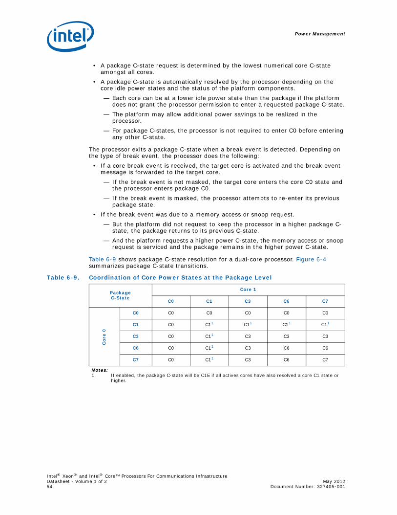
Power Management
Intel® Xeon® and Intel® Core™ Processors For Communications InfrastructureDatasheet - Volume 1 of 2 May 201254 Document Number: 327405-001
• A package C-state request is determined by the lowest numerical core C-state amongst all cores.
• A package C-state is automatically resolved by the processor depending on the core idle power states and the status of the platform components.— Each core can be at a lower idle power state than the package if the platform
does not grant the processor permission to enter a requested package C-state.— The platform may allow additional power savings to be realized in the
processor.— For package C-states, the processor is not required to enter C0 before entering
any other C-state.
The processor exits a package C-state when a break event is detected. Depending on the type of break event, the processor does the following:
• If a core break event is received, the target core is activated and the break event message is forwarded to the target core.— If the break event is not masked, the target core enters the core C0 state and
the processor enters package C0.— If the break event is masked, the processor attempts to re-enter its previous
package state.• If the break event was due to a memory access or snoop request.
— But the platform did not request to keep the processor in a higher package C-state, the package returns to its previous C-state.
— And the platform requests a higher power C-state, the memory access or snoop request is serviced and the package remains in the higher power C-state.
Table 6-9 shows package C-state resolution for a dual-core processor. Figure 6-4 summarizes package C-state transitions.
Table 6-9. Coordination of Core Power States at the Package Level
PackageC-State
Core 1
C0 C1 C3 C6 C7
Co
re 0
C0 C0 C0 C0 C0 C0
C1 C0 C11 C11 C11 C11
C3 C0 C11 C3 C3 C3
C6 C0 C11 C3 C6 C6
C7 C0 C11 C3 C6 C7
Notes:1. If enabled, the package C-state will be C1E if all actives cores have also resolved a core C1 state or
higher.
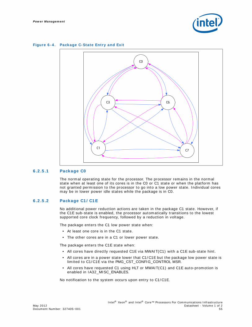
Power Management
Intel® Xeon® and Intel® Core™ Processors For Communications InfrastructureMay 2012 Datasheet - Volume 1 of 2Document Number: 327405-001 55
6.2.5.1 Package C0
The normal operating state for the processor. The processor remains in the normal state when at least one of its cores is in the C0 or C1 state or when the platform has not granted permission to the processor to go into a low power state. Individual cores may be in lower power idle states while the package is in C0.
6.2.5.2 Package C1/C1E
No additional power reduction actions are taken in the package C1 state. However, if the C1E sub-state is enabled, the processor automatically transitions to the lowest supported core clock frequency, followed by a reduction in voltage.
The package enters the C1 low power state when:• At least one core is in the C1 state.• The other cores are in a C1 or lower power state.
The package enters the C1E state when:• All cores have directly requested C1E via MWAIT(C1) with a C1E sub-state hint.• All cores are in a power state lower that C1/C1E but the package low power state is
limited to C1/C1E via the PMG_CST_CONFIG_CONTROL MSR.• All cores have requested C1 using HLT or MWAIT(C1) and C1E auto-promotion is
enabled in IA32_MISC_ENABLES.
No notification to the system occurs upon entry to C1/C1E.
Figure 6-4. Package C-State Entry and Exit
C0
C1
C6
C7
C3
Power Management
Intel® Xeon® and Intel® Core™ Processors For Communications InfrastructureDatasheet - Volume 1 of 2 May 201256 Document Number: 327405-001
6.2.5.3 Package C3 State
A processor enters the package C3 low power state when:• At least one core is in the C3 state.• The other cores are in a C3 or lower power state, and the processor has been
granted permission by the platform. • The platform has not granted a request to a package C6/C7 state but has allowed a
package C6 state.
In package C3-state, the L3 shared cache is snoopable.
6.2.5.4 Package C6 State
A processor enters the package C6 low power state when:• At least one core is in the C6 state.• The other cores are in a C6 or lower power state, and the processor has been
granted permission by the platform.• The platform has not granted a package C7 request but has allowed a C6 package
state.
In package C6 state, all cores have saved their architectural state and have had their core voltages reduced to zero volts. The L3 shared cache is still powered and snoopable in this state. The processor remains in package C6 state as long as any part of the L3 cache is active.
6.2.5.5 Package C7 State
The processor enters the package C7 low power state when all cores are in the C7 state and the L3 cache is completely flushed. The last core to enter the C7 state begins to shrink the L3 cache by N-ways until the entire L3 cache has been emptied. This allows further power savings.
Core break events are handled the same way as in package C3 or C6. However, snoops are not sent to the processor in package C7 state because the platform, by granting the package C7 state, has acknowledged that the processor possesses no snoopable information. This allows the processor to remain in this low power state and maximize its power savings.
Upon exit of the package C7 state, the L3 cache is not immediately re-enabled. It re-enables once the processor has stayed out of the C6 or C7 for an preset amount of time. Power is saved since this prevents the L3 cache from being re-populated only to be immediately flushed again.
6.2.5.6 Dynamic L3 Cache Sizing
Upon entry into the package C7 state, the L3 cache is reduced by N-ways until it is completely flushed. The number of ways, N, is dynamically chosen per concurrent C7 entry. Similarly, upon exit, the L3 cache is gradually expanded based on internal heuristics.
Power Management
Intel® Xeon® and Intel® Core™ Processors For Communications InfrastructureMay 2012 Datasheet - Volume 1 of 2Document Number: 327405-001 57
6.3 IMC Power ManagementThe main memory is power managed during normal operation and in low-power ACPI Cx states.
6.3.1 Disabling Unused System Memory Outputs
Any system memory (SM) interface signal that goes to a memory module connector in which it is not connected to any actual memory devices (such as DIMM connector is unpopulated, or is single-sided) is tri-stated. The benefits of disabling unused SM signals are:
• Reduced power consumption.• Reduced possible overshoot/undershoot signal quality issues seen by the processor
I/O buffer receivers caused by reflections from potentially un-terminated transmission lines.
When a given rank is not populated, the corresponding chip select and CKE signals are not driven.
At reset, all rows must be assumed to be populated, until it can be proven that they are not populated. This is due to the fact that when CKE is tristated with an DIMM present, the DIMM is not guaranteed to maintain data integrity.
SCKE tristate should be enabled by BIOS where appropriate, since at reset all rows must be assumed to be populated.
6.3.2 DRAM Power Management and Initialization
The processor implements extensive support for power management on the SDRAM interface. There are four SDRAM operations associated with the Clock Enable (CKE) signals, which the SDRAM controller supports. The processor drives four CKE pins to perform these operations.
The CKE is one of the power-save means. When CKE is off the internal DDR clock is disabled and the DDR power is reduced. The power-saving differs according to the selected mode and the DDR type used. For more information, see the IDD table in the DDR specification.
The DDR specification defines 3 levels of power-down that differ in power-saving and in wakeup time:1. Active power-down (APD): This mode is entered if there are open pages when
deasserting CKE. In this mode the open pages are retained. Power-saving in this mode is the lowest. Power consumption of DDR is defined by IDD3P. Exiting this mode is defined by tXP – small number of cycles.
2. Precharged power-down (PPD): This mode is entered if all banks in DDR are precharged when de-asserting CKE. Power-saving in this mode is intermediate –better than APD, but less than DLL-off. Power consumption is defined by IDD2P1. Exiting this mode is defined by tXP. Difference from APD mode is that when waking-up all page-buffers are empty.
3. DLL-off: In this mode the data-in DLLs on DDR are off. Power-saving in this mode is the best among all power-modes. Power consumption is defined by IDD2P1. Exiting this mode is defined by tXP, but also tXPDLL (10 – 20 according to DDR type) cycles until first data transfer is allowed.
The processor supports 6 different types of power-down. These different modes are the power-down modes supported by DDR3 and combinations of these modes. The type of CKE power-down is defined by the configuration. The options are:
Power Management
Intel® Xeon® and Intel® Core™ Processors For Communications InfrastructureDatasheet - Volume 1 of 2 May 201258 Document Number: 327405-001
1. No power-down.2. APD: The rank enters power-down as soon as idle-timer expires, no matter what is
the bank status.3. PPD: When idle timer expires the MC sends PRE-all to rank and then enters
powerdown.4. DLL-off: same as option (2) but DDR is configured to DLL-off.5. APD, change to PPD (APD-PPD): Begins as option (1), and when all page-close
timers of the rank are expired, it wakes the rank, issues PRE-all, and returns to PPD.
6. APD, change to DLL-off (APD_DLLoff) – Begins as option (1), and when all page-close timers of the rank are expired, it wakes the rank, issues PRE-all and returns to DLL-off power-down.
The CKE is determined per rank when it is inactive. Each rank has an idle-counter. The idle-counter starts counting as soon as the rank has no accesses, and if it expires, the rank may enter power-down while no new transactions to the rank arrive to queues. The idle-counter begins counting at the last incoming transaction arrival.
It is important to understand that since the power-down decision is per rank, the MC can find many opportunities to power-down ranks even while running memory intensive applications, and savings are significant (may be a few watts, according to the DDR specification). This is significant when each channel is populated with more ranks.
Selection of power modes should be according to power-performance or thermal tradeoffs of a given system:
• When trying to achieve maximum performance and power or thermal consideration is not an issue: use no power-down.
• In a system that tries to minimize power-consumption, try to use the deepest power-down mode possible – DLL-off or APD_DLLoff.
• In high-performance systems with dense packaging (that is, complex thermal design) the power-down mode should be considered in order to reduce the heating and avoid DDR throttling caused by the heating.
Control of the power-mode must be controlled through the BIOS – The BIOS selects no-powerdown by default. There are knobs to change the power-down selected mode.
Another control is the idle timer expiration count. This is set through PM_PDWN_config bits 7:0 (MCHBAR +4CB0). As this timer is set to a shorter time, the MC will have more opportunities to put DDR in power-down. The minimum recommended value for this register is 15. There is no BIOS hook to set this register. Customers who choose to change the value of this register can do it by changing the BIOS. For experiments, this register can be modified in real time if BIOS did not lock the MC registers.
Note: In APD, APD-PPD, and APD_DLL-off, there is no point in setting the idle-counter in the same range as page-close idle timer.
Another option associated with CKE power-down is the S_DLL-off. When this option is enabled, the SBR I/O slave DLLs go off when all channel ranks are in power-down. (Do not confuse it with the DLL-off mode in which the DDR DLLs are off). This mode requires you to define the I/O slave DLL wakeup time.
Power Management
Intel® Xeon® and Intel® Core™ Processors For Communications InfrastructureMay 2012 Datasheet - Volume 1 of 2Document Number: 327405-001 59
6.3.2.1 Initialization Role of CKE
During power-up, CKE is the only input to the SDRAM that has its level is recognized (other than the DDR3 reset pin) once power is applied. It must be driven LOW by the DDR controller to make sure the SDRAM components float DQ and DQS during power-up. CKE signals remain LOW (while any reset is active) until the BIOS writes to a configuration register. Using this method, CKE is guaranteed to remain inactive for much longer than the specified 200 micro-seconds after power and clocks to SDRAM devices are stable.
6.3.2.2 Dynamic Power Down Operation
Dynamic power-down of memory is employed during normal operation. Based on idle conditions, a given memory rank may be powered down. The IMC implements aggressive CKE control to dynamically put the DRAM devices in a power down state. The processor core controller can be configured to put the devices in active power-down (CKE deassertion with open pages) or precharge power-down (CKE deassertion with all pages closed). Precharge power-down provides greater power savings but has a bigger performance impact, since all pages will first be closed before putting the devices in power-down mode.
If dynamic power-down is enabled, all ranks are powered up before doing a refresh cycle and all ranks are powered down at the end of refresh.
6.3.2.3 DRAM I/O Power Management
Unused signals should be disabled to save power and reduce electromagnetic interference. This includes all signals associated with an unused memory channel. Clocks can be controlled on a per DIMM basis. Exceptions are made for per DIMM control signals such as CS#, CKE, and ODT for unpopulated DIMM slots.
The I/O buffer for an unused signal should be tri-stated (output driver disabled), the input receiver (differential sense-amp) should be disabled, and any DLL circuitry related ONLY to unused signals should be disabled. The input path must be gated to prevent spurious results due to noise on the unused signals (typically handled automatically when input receiver is disabled).
6.4 PCIe* Power Management• Active power management support using L0s, and L1 states.• All inputs and outputs disabled in L2/L3 Ready state.
Note: PCIe* interface does not support Hot Plug.
Note: Power impact may be observed when PCIe* link disable power management state is used.
6.5 DMI Power ManagementActive power management support using L0s/L1 state.
6.6 Thermal Power Management See Section 7.0, “Thermal Management” on page 61 for all thermal power management-related features.
§ §
Power Management
Intel® Xeon® and Intel® Core™ Processors For Communications InfrastructureDatasheet - Volume 1 of 2 May 201260 Document Number: 327405-001
Thermal Management
Intel® Xeon® and Intel® Core™ Processors For Communications InfrastructureMay 2012 Datasheet - Volume 1 of 2Document Number: 327405-001 61
7.0 Thermal Management
The thermal solution provides both the component-level and the system-level thermal management. To allow for the optimal operation and long-term reliability of Intel processor-based systems, the system/processor thermal solution should be designed so that the processor:
• Remains below the maximum junction temperature (TJ-MAX) specification at the maximum Thermal Design Power (TDP).
• Conforms to system constraints, such as system acoustics, system skin-temperatures, and exhaust-temperature requirements.
Caution: Thermal specifications given in this chapter are on the component and package level and apply specifically to the processor. Operating the processor outside the specified limits may result in permanent damage to the processor and potentially other components in the system.
7.1 Thermal Design Power (TDP) andJunction Temperature (TJ)The processor TDP is the maximum sustained power that should be used for design of the processor thermal solution. TDP represents an expected maximum sustained power from realistic applications. TDP may be exceeded for short periods of time or if running a “power virus” workload.
The processor integrates multiple CPU on a single die. This may result in differences in the power distribution across the die and must be considered when designing the thermal solution. See the 2nd Generation Intel® Core™ Processor For Communications Infrastructure Thermal/Mechanical Design Guide for more details.
7.2 Thermal and Power SpecificationsThe following notes apply to Table 7-1 and Table 7-2.
Note Definition
1The TDPs given are not the maximum power the processor can generate. Analysis indicates that real applications are unlikely to cause the processor to consume the theoretical maximum power dissipation for sustained periods of time.
2The thermal solution needs to ensure that the processor temperature does not exceed the maximum junction temperature (Tj,max) limit, as measured by the DTS and the critical temperature bit.
3 The processor junction temperature is monitored by Digital Temperature Sensors (DTS). For DTS accuracy, see Section 7.3.1.2.1.
4Digital Thermal Sensor (DTS) based fan speed control is required to achieve optimal thermal performance. Intel recommends full cooling capability well before the DTS reading reaches Tj,Max. An example of this would be Tj,Max - 10ºC.
5 At Tj of Tj,max
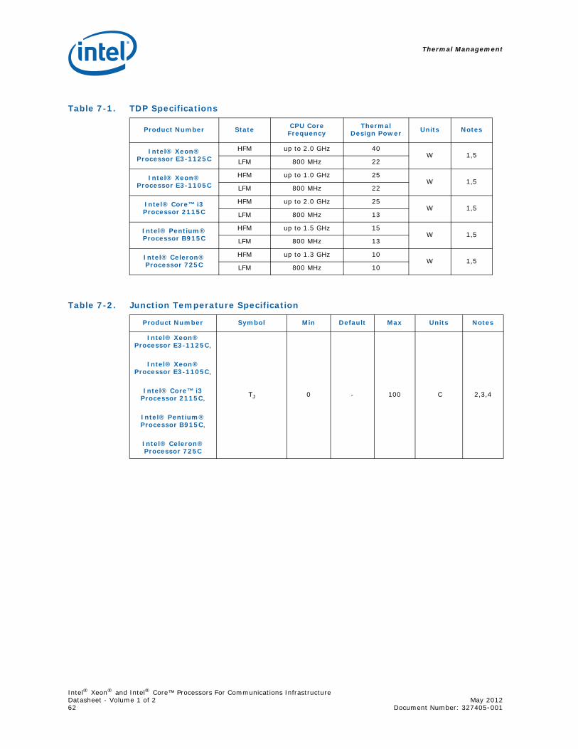
Thermal Management
Intel® Xeon® and Intel® Core™ Processors For Communications InfrastructureDatasheet - Volume 1 of 2 May 201262 Document Number: 327405-001
Table 7-1. TDP Specifications
Product Number State CPU Core Frequency
Thermal Design Power Units Notes
Intel® Xeon® Processor E3-1125C
HFM up to 2.0 GHz 40W 1,5
LFM 800 MHz 22
Intel® Xeon® Processor E3-1105C
HFM up to 1.0 GHz 25W 1,5
LFM 800 MHz 22
Intel® Core™ i3 Processor 2115C
HFM up to 2.0 GHz 25W 1,5
LFM 800 MHz 13
Intel® Pentium® Processor B915C
HFM up to 1.5 GHz 15W 1,5
LFM 800 MHz 13
Intel® Celeron® Processor 725C
HFM up to 1.3 GHz 10W 1,5
LFM 800 MHz 10
Table 7-2. Junction Temperature Specification
Product Number Symbol Min Default Max Units Notes
Intel® Xeon® Processor E3-1125C,
Intel® Xeon® Processor E3-1105C,
Intel® Core™ i3 Processor 2115C,
Intel® Pentium® Processor B915C,
Intel® Celeron® Processor 725C
TJ 0 - 100 C 2,3,4
Thermal Management
Intel® Xeon® and Intel® Core™ Processors For Communications InfrastructureMay 2012 Datasheet - Volume 1 of 2Document Number: 327405-001 63
7.3 Thermal Management FeaturesThis section covers thermal management features for the processor.
7.3.1 Processor Package Thermal Features
This section covers thermal management features for the entire processor complex (including the processor core and integrated memory controller hub) and is referred to as processor package or package.
Occasionally the package operates in conditions that exceed its maximum allowable operating temperature. This can be due to internal overheating or due to overheating in the entire system. In order to protect itself and the system from thermal failure, the package is capable of reducing its power consumption and thereby its temperature to attempt to remain within normal operating limits via the Adaptive Thermal Monitor.
The Adaptive Thermal Monitor can be activated when any package temperature, monitored by a digital thermal sensor (DTS), meets or exceeds its maximum junction temperature specification (TJ-MAX) and asserts PROCHOT#. The thermal control circuit (TCC) can be activated prior to TJ-MAX by use of the TCC activation offset. The assertion of PROCHOT# activates the Thermal Control Circuit (TCC), and causes the processor core to reduce frequency and voltage adaptively. The TCC remains active as long as any package temperature exceeds its specified limit. Therefore, the Adaptive Thermal Monitor continues to reduce the package frequency and voltage until the TCC is de-activated. If properly configured, when an external device asserts PROCHOT# the thermal control circuit (TCC) causes the processor core to reduce frequency and voltage adaptively.
Note: Adaptive Thermal Monitor is always enabled.
7.3.1.1 Adaptive Thermal Monitor
The purpose of the Adaptive Thermal Monitor is to reduce processor core power consumption and temperature until it operates at or below its maximum operating temperature (according for TCC activation offset). Processor core power reduction is achieved by:
• Adjusting the operating frequency (via the core ratio multiplier) and input voltage (via the SVID bus).
• Modulating (starting and stopping) the internal processor core clocks (duty cycle).
The temperature at which the Adaptive Thermal Monitor activates the Thermal Control Circuit is factory calibrated and is not user configurable. The default value is software visible in the TEMPERATURE_TARGET (0x1A2) MSR, Bits 23:16. The Adaptive Thermal Monitor does not require any additional hardware, software drivers, or interrupt handling routines.
Note: The Adaptive Thermal Monitor is not intended as a mechanism to maintain processor TDP. The system design should provide a thermal solution that can maintain TDP within its intended usage range.
7.3.1.1.1 Frequency/Voltage Control
Upon TCC activation, the processor core attempts to dynamically reduce processor core power by lowering the frequency and voltage operating point. The operating points are automatically calculated by the processor core itself and do not require the BIOS to program them as with previous generations of Intel processors. The processor core scales the operating points so that:
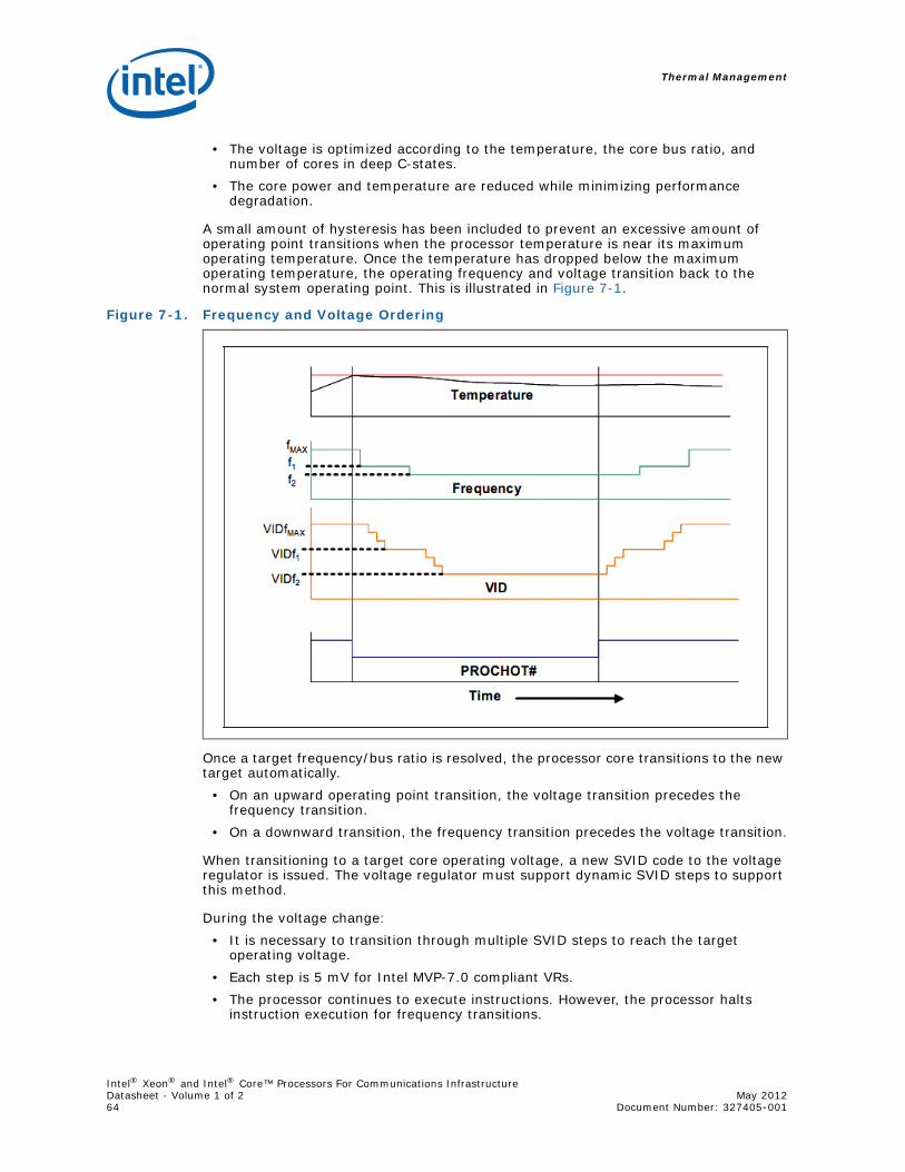
Thermal Management
Intel® Xeon® and Intel® Core™ Processors For Communications InfrastructureDatasheet - Volume 1 of 2 May 201264 Document Number: 327405-001
• The voltage is optimized according to the temperature, the core bus ratio, and number of cores in deep C-states.
• The core power and temperature are reduced while minimizing performance degradation.
A small amount of hysteresis has been included to prevent an excessive amount of operating point transitions when the processor temperature is near its maximum operating temperature. Once the temperature has dropped below the maximum operating temperature, the operating frequency and voltage transition back to the normal system operating point. This is illustrated in Figure 7-1.
Once a target frequency/bus ratio is resolved, the processor core transitions to the new target automatically.
• On an upward operating point transition, the voltage transition precedes the frequency transition.
• On a downward transition, the frequency transition precedes the voltage transition.
When transitioning to a target core operating voltage, a new SVID code to the voltage regulator is issued. The voltage regulator must support dynamic SVID steps to support this method.
During the voltage change:• It is necessary to transition through multiple SVID steps to reach the target
operating voltage.• Each step is 5 mV for Intel MVP-7.0 compliant VRs.• The processor continues to execute instructions. However, the processor halts
instruction execution for frequency transitions.
Figure 7-1. Frequency and Voltage Ordering
Thermal Management
Intel® Xeon® and Intel® Core™ Processors For Communications InfrastructureMay 2012 Datasheet - Volume 1 of 2Document Number: 327405-001 65
If a processor load-based Enhanced Intel SpeedStep Technology/P-state transition (through MSR write) is initiated while the Adaptive Thermal Monitor is active, there are two possible outcomes:
• If the P-state target frequency is higher than the processor core optimized target frequency, the p-state transition is deferred until the thermal event has been completed.
• If the P-state target frequency is lower than the processor core optimized target frequency, the processor transitions to the P-state operating point.
7.3.1.1.2 Clock Modulation
If the frequency/voltage changes are unable to end an Adaptive Thermal Monitor event, the Adaptive Thermal Monitor utilizes clock modulation. Clock modulation is done by alternately turning the clocks off and on at a duty cycle (ratio between clock “on” time and total time) specific to the processor. The duty cycle is factory configured to 25% on and 75% off and cannot be modified. The period of the duty cycle is configured to 32 microseconds when the TCC is active. Cycle times are independent of processor frequency. A small amount of hysteresis has been included to prevent excessive clock modulation when the processor temperature is near its maximum operating temperature. Once the temperature has dropped below the maximum operating temperature, and the hysteresis timer has expired, the TCC goes inactive and clock modulation ceases. Clock modulation is automatically engaged as part of the TCC activation when the frequency/voltage targets are at their minimum settings. Processor performance decreases by the same amount as the duty cycle when clock modulation is active. Snooping and interrupt processing are performed in the normal manner while the TCC is active.
7.3.1.2 Digital Thermal Sensor
Each processor execution core has an on-die Digital Thermal Sensor (DTS) which detects the core’s instantaneous temperature. The DTS is the preferred method of monitoring processor die temperature because
• It is located near the hottest portions of the die.• It can accurately track the die temperature and ensure that the Adaptive Thermal
Monitor is not excessively activated.
Temperature values from the DTS can be retrieved through• A software interface via processor Model Specific Register (MSR). • A processor hardware interface as described in Section 7.3.4, “Platform
Environment Control Interface (PECI)”.
Note: When temperature is retrieved by processor MSR, it is the instantaneous temperature of the given core. When temperature is retrieved via PECI, it is the average of the highest DTS temperature in the package over a 256 ms time window. Intel recommends using the PECI reported temperature for platform thermal control that benefits from averaging, such as fan speed control. The average DTS temperature may not be a good indicator of package Adaptive Thermal Monitor activation or rapid increases in temperature that triggers the Out of Specification status bit within the PACKAGE_THERM_STATUS MSR 01B1h and IA32_THERM_STATUS MSR 19Ch.
Code execution is halted in C1-C7. Therefore temperature cannot be read via the processor MSR without bringing a core back into C0. However, temperature can still be monitored through PECI in lower C-states except for C7.
Thermal Management
Intel® Xeon® and Intel® Core™ Processors For Communications InfrastructureDatasheet - Volume 1 of 2 May 201266 Document Number: 327405-001
Unlike traditional thermal devices, the DTS outputs a temperature relative to the maximum supported operating temperature of the processor (TJ-MAX), regardless of TCC activation offset. It is the responsibility of software to convert the relative temperature to an absolute temperature. The absolute reference temperature is readable in the TEMPERATURE_TARGET MSR 1A2h. The temperature returned by the DTS is an implied negative integer indicating the relative offset from TJ-MAX. The DTS does not report temperatures greater than TJ-MAX.
The DTS-relative temperature readout directly impacts the Adaptive Thermal Monitor trigger point. When a package DTS indicates that it has reached the TCC activation (a reading of 0x0, except when the TCC activation offset is changed), the TCC activates and indicates an Adaptive Thermal Monitor event. A TCC activation lowers the IA core frequency, voltage or both.
Changes to the temperature can be detected via two programmable thresholds located in the processor thermal MSRs. These thresholds have the capability of generating interrupts via the core's local APIC. See the Intel® 64 and IA-32 Architectures Software Developer's Manuals for specific register and programming details.
7.3.1.2.1 Digital Thermal Sensor Accuracy (Taccuracy)
The error associated with DTS measurement does not exceed ±5°C at TJ-MAX. The DTS measurement within the entire operating range meets a ±5°C accuracy.
7.3.1.3 PROCHOT# Signal
PROCHOT# (processor hot) is asserted when the processor core temperature has reached its maximum operating temperature (TJ-MAX). See Figure 7-1 for a timing diagram of the PROCHOT# signal assertion relative to the Adaptive Thermal Response. Only a single PROCHOT# pin exists at a package level. When any core arrives at the TCC activation point, the PROCHOT# signal is asserted. PROCHOT# assertion policies are independent of Adaptive Thermal Monitor enabling.
Note: Bus snooping and interrupt latching are active while the TCC is active.
7.3.1.3.1 Bi-Directional PROCHOT#
By default, the PROCHOT# signal is defined as an output only. However, the signal may be configured as bi-directional. When configured as a bi-directional signal, PROCHOT# can be used for thermally protecting other platform components should they overheat as well. When PROCHOT# is driven by an external device:
• The package immediately transitions to the minimum operation points (voltage and frequency) supported by the processor cores. This is contrary to the internally-generated Adaptive Thermal Monitor response.
• Clock modulation is not activated.
The TCC remains active until the system deasserts PROCHOT#. The processor can be configured to generate an interrupt upon assertion and deassertion of the PROCHOT# signal.
Note: Toggling PROCHOT# more than once in 1.5ms period results in constant Pn state of the processor.
7.3.1.3.2 Voltage Regulator Protection
PROCHOT# may be used for thermal protection of voltage regulators (VR). System designers can create a circuit to monitor the VR temperature and activate the TCC when the temperature limit of the VR is reached. By asserting PROCHOT# (pulled-low) and activating the TCC, the VR cools down as a result of reduced processor power
Thermal Management
Intel® Xeon® and Intel® Core™ Processors For Communications InfrastructureMay 2012 Datasheet - Volume 1 of 2Document Number: 327405-001 67
consumption. Bi-directional PROCHOT# can allow VR thermal designs to target thermal design current (ICCTDC) instead of maximum current. Systems should still provide proper cooling for the VR and rely on bi-directional PROCHOT# only as a backup in case of system cooling failure. Overall, the system thermal design should allow the power delivery circuitry to operate within its temperature specification even while the processor is operating at its TDP.
7.3.1.3.3 Thermal Solution Design and PROCHOT# Behavior
With a properly designed and characterized thermal solution, it is anticipated that PROCHOT# is only asserted for very short periods of time when running the most power intensive applications. The processor performance impact due to these brief periods of TCC activation is expected to be so minor that it would be immeasurable.
However, an under-designed thermal solution that is not able to prevent excessive assertion of PROCHOT# in the anticipated ambient environment may:
• Cause a noticeable performance loss.• Result in prolonged operation at or above the specified maximum junction
temperature and affect the long-term reliability of the processor.• May be incapable of cooling the processor even when the TCC is active continuously
(in extreme situations).
See the 2nd Generation Intel® Core™ Processor For Communications Infrastructure Thermal/Mechanical Design Guide for information on implementing the bi-directional PROCHOT# feature and designing a compliant thermal solution.
7.3.1.3.4 Low-Power States and PROCHOT# Behavior
If the processor enters a low-power package idle state such as C3 or C6/C7 with PROCHOT# asserted, PROCHOT# remains asserted until:
• The processor exits the low-power state• The processor junction temperature drops below the thermal trip point.
For the package C7 state, PROCHOT# may deassert for the duration of C7 state residency even if the processor enters the idle state operating at the TCC activation temperature. The PECI interface is fully operational during all C-states and it is expected that the platform continues to manage processor (“package”) core thermals even during idle states by regularly polling for thermal data over PECI.
7.3.1.3.5 THERMTRIP# Signal
Regardless of enabling the automatic or on-demand modes, in the event of a catastrophic cooling failure, the package automatically shuts down when the silicon has reached an elevated temperature that risks physical damage to the product. At this point the THERMTRIP# signal is active.
7.3.1.3.6 Critical Temperature Detection
Critical Temperature detection is performed by monitoring the package temperature. This feature is intended for graceful shutdown before the THERMTRIP# is activated, however, the processor execution is not guaranteed between critical temperature and THERMTRIP#. If the package's Adaptive Thermal Monitor is triggered and the temperature remains high, a critical temperature status and sticky bit are latched in the PACKAGE_THERM_STATUS MSR 1B1h and also generates a thermal interrupt if enabled. For more details on the interrupt mechanism, see the Intel® 64 and IA-32 Architectures Software Developer's Manuals.
Thermal Management
Intel® Xeon® and Intel® Core™ Processors For Communications InfrastructureDatasheet - Volume 1 of 2 May 201268 Document Number: 327405-001
7.3.2 Processor Core Specific Thermal Features
7.3.2.1 On-Demand Mode
The processor provides an auxiliary mechanism that allows system software to force the processor to reduce its power consumption via clock modulation. This mechanism is referred to as “On-Demand” mode and is distinct from Adaptive Thermal Monitor and bi-directional PROCHOT#. Processor platforms must not rely on software usage of this mechanism to limit the processor temperature. On-Demand Mode can be done via processor MSR or chipset I/O emulation.
On-Demand Mode may be used in conjunction with the Adaptive Thermal Monitor. However, if the system software tries to enable On-Demand mode at the same time the TCC is engaged, the factory configured duty cycle of the TCC overrides the duty cycle selected by the On-Demand mode. If the I/O based and MSR-based On-Demand modes are in conflict, the duty cycle selected by the I/O emulation-based On-Demand mode takes precedence over the MSR-based On-Demand Mode.
7.3.2.1.1 MSR Based On-Demand Mode
If Bit 4 of the IA32_CLOCK_MODULATION MSR is set to a 1, the processor immediately reduces its power consumption via modulation of the internal core clock, independent of the processor temperature. The duty cycle of the clock modulation is programmable via Bits 3:1 of the same IA32_CLOCK_MODULATION MSR. In this mode, the duty cycle can be programmed in either 12.5% or 6.25% increments (discoverable via CPU ID). Thermal throttling using this method modulates each processor core’s clock independently.
7.3.2.1.2 I/O Emulation-Based On-Demand Mode
I/O emulation-based clock modulation provides legacy support for operating system software that initiates clock modulation through I/O writes to ACPI defined processor clock control registers on the chipset (PROC_CNT). Thermal throttling using this method modulates all processor cores simultaneously.
7.3.3 Memory Controller Specific Thermal Features
The memory controller provides the ability to initiate memory throttling based upon memory temperature. The memory temperature can be provided to the memory controller via PECI or can be estimated by the memory controller based upon memory activity. The temperature trigger points are programmable by memory mapped IO registers.
7.3.3.1 Programmable Trip Points
This memory controller provides programmable critical, hot and warm trip points. Crossing a critical trip point forces a system shutdown. Crossing a hot or warm trip point initiates throttling. The amount of memory throttle at each trip point is programmable.
7.3.4 Platform Environment Control Interface (PECI)
The Platform Environment Control Interface (PECI) is a one-wire interface that provides a communication channel between Intel processor and chipset components to external monitoring devices. The processor implements a PECI interface to allow communication of processor thermal information to other devices on the platform. The processor provides a digital thermal sensor (DTS) for fan speed control. The DTS is calibrated at the factory to provide a digital representation of relative processor temperature. Averaged DTS values are read via the PECI interface.
Thermal Management
Intel® Xeon® and Intel® Core™ Processors For Communications InfrastructureMay 2012 Datasheet - Volume 1 of 2Document Number: 327405-001 69
The PECI physical layer is a self-clocked one-wire bus that begins each bit with a driven, rising edge from an idle level near zero volts. The duration of the signal driven high depends on whether the bit value is a Logic 0 or Logic 1. PECI also includes variable data transfer rate established with every message. The single wire interface provides low board routing overhead for the multiple load connections in the congested routing area near the processor and chipset components. Bus speed, error checking, and low protocol overhead provides adequate link bandwidth and reliability to transfer critical device operating conditions and configuration information.
7.3.4.1 Fan Speed Control with Digital Thermal Sensor
Digital Thermal Sensor based fan speed control (TFAN) is a recommended feature to achieve optimal thermal performance. At the TFAN temperature, Intel recommends full cooling capability well before the DTS reading reaches TJ-MAX. An example of this would be TFAN = TJ, Max - 10ºC.
§ §

Thermal Management
Intel® Xeon® and Intel® Core™ Processors For Communications InfrastructureDatasheet - Volume 1 of 2 May 201270 Document Number: 327405-001
Signal Description
Intel® Xeon® and Intel® Core™ Processors For Communications InfrastructureMay 2012 Datasheet - Volume 1 of 2Document Number: 327405-001 71
8.0 Signal Description
This chapter describes the processor signals. They are arranged in functional groups according to their associated interface or category. The following notations are used to describe the signal type:
The signal description also includes the type of buffer used for the particular signal.
8.1 System Memory Interface
Notations Signal Type
I Input Pin
O Output Pin
I/O Bi-directional Input/Output Pin
Table 8-1. Signal Description Buffer Types
Signal Description
PCI Express*PCI Express* interface signals. These signals are compatible with PCI Express* 2.0 Signalling Environment AC Specifications and are AC coupled. The buffers are not 3.3-V tolerant. See the PCIe* specification.
DMIDirect Media Interface signals. These signals are compatible with PCI Express* 2.0 Signaling Environment AC Specifications, but are DC coupled. The buffers are not 3.3-V tolerant.
CMOS CMOS buffers. 1.1-V tolerant
DDR3 DDR3 buffers: 1.5-V tolerant
A Analog reference or output. May be used as a threshold voltage or for buffer compensation
Ref Voltage reference signal
Asynchronous1 Signal has no timing relationship with any reference clock.
Notes:1. Qualifier for a buffer type.
Table 8-2. Memory Channel A (Sheet 1 of 2)
Signal Name Description Direction/Buffer Type
SA_BS[2:0] Bank Select: These signals define which banks are selected within each SDRAM rank.
ODDR3
SA_WE#Write Enable Control Signal: Used with SA_RAS# and SA_CAS# (along with SA_CS#) to define the SDRAM Commands.
ODDR3
SA_RAS#RAS Control Signal: Used with SA_CAS# and SA_WE# (along with SA_CS#) to define the SRAM Commands.
ODDR3
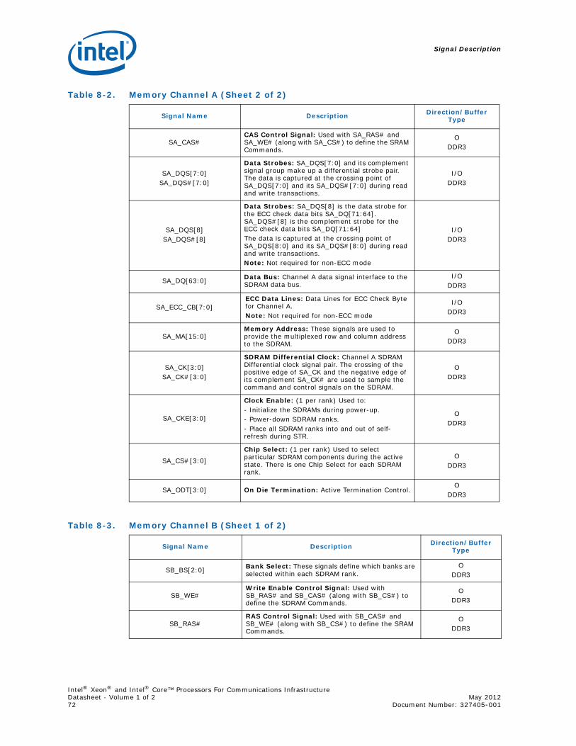
Signal Description
Intel® Xeon® and Intel® Core™ Processors For Communications InfrastructureDatasheet - Volume 1 of 2 May 201272 Document Number: 327405-001
SA_CAS#CAS Control Signal: Used with SA_RAS# and SA_WE# (along with SA_CS#) to define the SRAM Commands.
ODDR3
SA_DQS[7:0] SA_DQS#[7:0]
Data Strobes: SA_DQS[7:0] and its complement signal group make up a differential strobe pair. The data is captured at the crossing point of SA_DQS[7:0] and its SA_DQS#[7:0] during read and write transactions.
I/ODDR3
SA_DQS[8] SA_DQS#[8]
Data Strobes: SA_DQS[8] is the data strobe for the ECC check data bits SA_DQ[71:64]. SA_DQS#[8] is the complement strobe for the ECC check data bits SA_DQ[71:64]The data is captured at the crossing point of SA_DQS[8:0] and its SA_DQS#[8:0] during read and write transactions.Note: Not required for non-ECC mode
I/ODDR3
SA_DQ[63:0] Data Bus: Channel A data signal interface to the SDRAM data bus.
I/ODDR3
SA_ECC_CB[7:0]ECC Data Lines: Data Lines for ECC Check Byte for Channel A.Note: Not required for non-ECC mode
I/ODDR3
SA_MA[15:0]Memory Address: These signals are used to provide the multiplexed row and column address to the SDRAM.
ODDR3
SA_CK[3:0]SA_CK#[3:0]
SDRAM Differential Clock: Channel A SDRAM Differential clock signal pair. The crossing of the positive edge of SA_CK and the negative edge of its complement SA_CK# are used to sample the command and control signals on the SDRAM.
ODDR3
SA_CKE[3:0]
Clock Enable: (1 per rank) Used to:- Initialize the SDRAMs during power-up.- Power-down SDRAM ranks.- Place all SDRAM ranks into and out of self-refresh during STR.
ODDR3
SA_CS#[3:0]
Chip Select: (1 per rank) Used to select particular SDRAM components during the active state. There is one Chip Select for each SDRAM rank.
ODDR3
SA_ODT[3:0] On Die Termination: Active Termination Control.O
DDR3
Table 8-3. Memory Channel B (Sheet 1 of 2)
Signal Name Description Direction/Buffer Type
SB_BS[2:0] Bank Select: These signals define which banks are selected within each SDRAM rank.
ODDR3
SB_WE#Write Enable Control Signal: Used with SB_RAS# and SB_CAS# (along with SB_CS#) to define the SDRAM Commands.
ODDR3
SB_RAS#RAS Control Signal: Used with SB_CAS# and SB_WE# (along with SB_CS#) to define the SRAM Commands.
ODDR3
Table 8-2. Memory Channel A (Sheet 2 of 2)
Signal Name Description Direction/Buffer Type
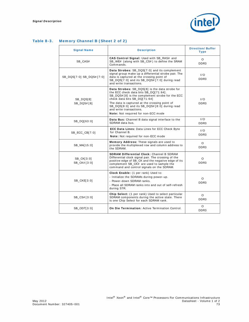
Signal Description
Intel® Xeon® and Intel® Core™ Processors For Communications InfrastructureMay 2012 Datasheet - Volume 1 of 2Document Number: 327405-001 73
SB_CAS#CAS Control Signal: Used with SB_RAS# and SB_WE# (along with SB_CS#) to define the SRAM Commands.
ODDR3
SB_DQS[7:0] SB_DQS#[7:0]
Data Strobes: SB_DQS[7:0] and its complement signal group make up a differential strobe pair. The data is captured at the crossing point of SB_DQS[7:0] and its SB_DQS#[7:0] during read and write transactions.
I/ODDR3
SB_DQS[8] SB_DQS#[8]
Data Strobes: SB_DQS[8] is the data strobe for the ECC check data bits SB_DQ[71:64]. SB_DQS#[8] is the complement strobe for the ECC check data bits SB_DQ[71:64]The data is captured at the crossing point of SB_DQS[8:0] and its SB_DQS#[8:0] during read and write transactions.Note: Not required for non-ECC mode
I/ODDR3
SB_DQ[63:0] Data Bus: Channel B data signal interface to the SDRAM data bus.
I/ODDR3
SB_ECC_CB[7:0]ECC Data Lines: Data Lines for ECC Check Byte for Channel B.Note: Not required for non-ECC mode
I/ODDR3
SB_MA[15:0]Memory Address: These signals are used to provide the multiplexed row and column address to the SDRAM.
ODDR3
SB_CK[3:0]SB_CK#[3:0]
SDRAM Differential Clock: Channel B SDRAM Differential clock signal pair. The crossing of the positive edge of SB_CK and the negative edge of its complement SB_CK# are used to sample the command and control signals on the SDRAM.
ODDR3
SB_CKE[3:0]
Clock Enable: (1 per rank) Used to:- Initialize the SDRAMs during power-up.- Power-down SDRAM ranks.- Place all SDRAM ranks into and out of self-refresh during STR.
ODDR3
SB_CS#[3:0]Chip Select: (1 per rank) Used to select particular SDRAM components during the active state. There is one Chip Select for each SDRAM rank.
ODDR3
SB_ODT[3:0] On Die Termination: Active Termination Control.O
DDR3
Table 8-3. Memory Channel B (Sheet 2 of 2)
Signal Name Description Direction/Buffer Type
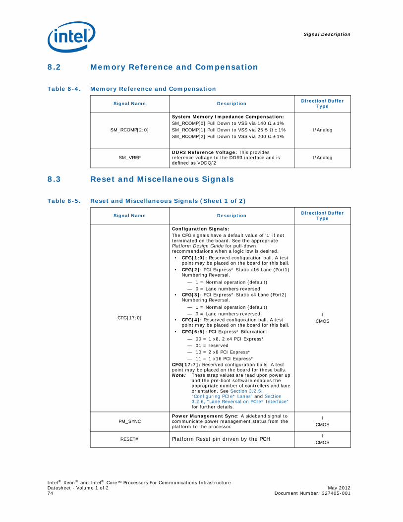
Signal Description
Intel® Xeon® and Intel® Core™ Processors For Communications InfrastructureDatasheet - Volume 1 of 2 May 201274 Document Number: 327405-001
8.2 Memory Reference and Compensation
8.3 Reset and Miscellaneous Signals
Table 8-4. Memory Reference and Compensation
Signal Name Description Direction/Buffer Type
SM_RCOMP[2:0]
System Memory Impedance Compensation: SM_RCOMP[0] Pull Down to VSS via 140 Ω ±1%SM_RCOMP[1] Pull Down to VSS via 25.5 Ω ±1%SM_RCOMP[2] Pull Down to VSS via 200 Ω ±1%
I/Analog
SM_VREFDDR3 Reference Voltage: This provides reference voltage to the DDR3 interface and is defined as VDDQ/2
I/Analog
Table 8-5. Reset and Miscellaneous Signals (Sheet 1 of 2)
Signal Name Description Direction/Buffer Type
CFG[17:0]
Configuration Signals:The CFG signals have a default value of '1' if not terminated on the board. See the appropriate Platform Design Guide for pull-down recommendations when a logic low is desired.• CFG[1:0]: Reserved configuration ball. A test
point may be placed on the board for this ball.• CFG[2]: PCI Express* Static x16 Lane (Port1)
Numbering Reversal.— 1 = Normal operation (default)— 0 = Lane numbers reversed
• CFG[3]: PCI Express* Static x4 Lane (Port2) Numbering Reversal.
— 1 = Normal operation (default)— 0 = Lane numbers reversed
• CFG[4]: Reserved configuration ball. A test point may be placed on the board for this ball.
• CFG[6:5]: PCI Express* Bifurcation:— 00 = 1 x8, 2 x4 PCI Express*— 01 = reserved— 10 = 2 x8 PCI Express*— 11 = 1 x16 PCI Express*
CFG[17:7]: Reserved configuration balls. A test point may be placed on the board for these balls.Note: These strap values are read upon power up
and the pre-boot software enables the appropriate number of controllers and lane orientation. See Section 3.2.5, “Configuring PCIe* Lanes” and Section 3.2.6, “Lane Reversal on PCIe* Interface” for further details.
ICMOS
PM_SYNCPower Management Sync: A sideband signal to communicate power management status from the platform to the processor.
ICMOS
RESET# Platform Reset pin driven by the PCH I CMOS
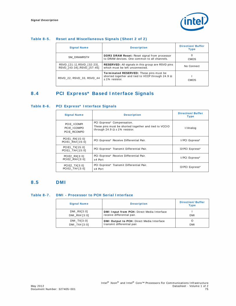
Signal Description
Intel® Xeon® and Intel® Core™ Processors For Communications InfrastructureMay 2012 Datasheet - Volume 1 of 2Document Number: 327405-001 75
8.4 PCI Express* Based Interface Signals
8.5 DMI
SM_DRAMRST# DDR3 DRAM Reset: Reset signal from processor to DRAM devices. One common to all channels.
0CMOS
RSVD_[21:1],RSVD_[32:23], RSVD_[43:34],RSVD_[57:45]
RESERVED: All signals in this group are RSVD pins which must be left unconnected. No Connect
RSVD_22, RSVD_33, RSVD_44
Terminated RESERVED: These pins must be shorted together and tied to VCCP through 24.9 Ω ±1% resistor.
ICMOS
Table 8-6. PCI Express* Interface Signals
Signal Name Description Direction/Buffer Type
PCIE_ICOMPIPCIE_ICOMPOPCIE_RCOMPO
PCI Express* Compensation.These pins must be shorted together and tied to VCCIO through 24.9 Ω ±1% resistor. I/Analog
PCIE1_RX[15:0]PCIE1_RX#[15:0] PCI Express* Receive Differential Pair. I/PCI Express*
PCIE1_TX[15:0]PCIE1_TX#[15:0] PCI Express* Transmit Differential Pair. O/PCI Express*
PCIE2_RX[3:0]PCIE2_RX#[3:0]
PCI Express* Receive Differential Pair.x4 Port
I/PCI Express*
PCIE2_TX[3:0]PCIE2_TX#[3:0]
PCI Express* Transmit Differential Pair.x4 Port
O/PCI Express*
Table 8-7. DMI - Processor to PCH Serial Interface
Signal Name Description Direction/Buffer Type
DMI_RX[3:0]DMI_RX#[3:0]
DMI Input from PCH: Direct Media Interface receive differential pair.
IDMI
DMI_TX[3:0]DMI_TX#[3:0]
DMI Output to PCH: Direct Media Interface transmit differential pair.
ODMI
Table 8-5. Reset and Miscellaneous Signals (Sheet 2 of 2)
Signal Name Description Direction/Buffer Type
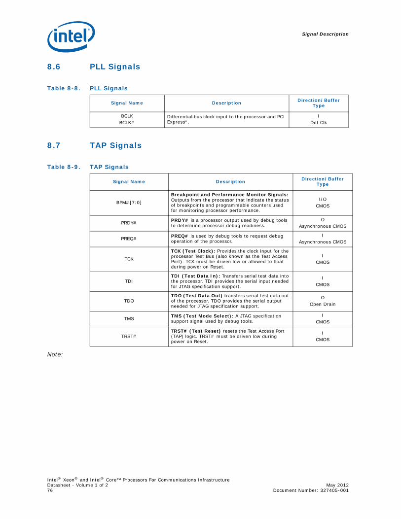
Signal Description
Intel® Xeon® and Intel® Core™ Processors For Communications InfrastructureDatasheet - Volume 1 of 2 May 201276 Document Number: 327405-001
8.6 PLL Signals
8.7 TAP Signals
Note:
Table 8-8. PLL Signals
Signal Name Description Direction/Buffer Type
BCLKBCLK#
Differential bus clock input to the processor and PCI Express*.
IDiff Clk
Table 8-9. TAP Signals
Signal Name Description Direction/Buffer Type
BPM#[7:0]
Breakpoint and Performance Monitor Signals: Outputs from the processor that indicate the status of breakpoints and programmable counters used for monitoring processor performance.
I/OCMOS
PRDY# PRDY# is a processor output used by debug tools to determine processor debug readiness.
OAsynchronous CMOS
PREQ# PREQ# is used by debug tools to request debug operation of the processor.
IAsynchronous CMOS
TCK
TCK (Test Clock): Provides the clock input for the processor Test Bus (also known as the Test Access Port). TCK must be driven low or allowed to float during power on Reset.
ICMOS
TDITDI (Test Data In): Transfers serial test data into the processor. TDI provides the serial input needed for JTAG specification support.
ICMOS
TDOTDO (Test Data Out) transfers serial test data out of the processor. TDO provides the serial output needed for JTAG specification support.
OOpen Drain
TMS TMS (Test Mode Select): A JTAG specification support signal used by debug tools.
ICMOS
TRST#TRST# (Test Reset) resets the Test Access Port (TAP) logic. TRST# must be driven low during power on Reset.
ICMOS
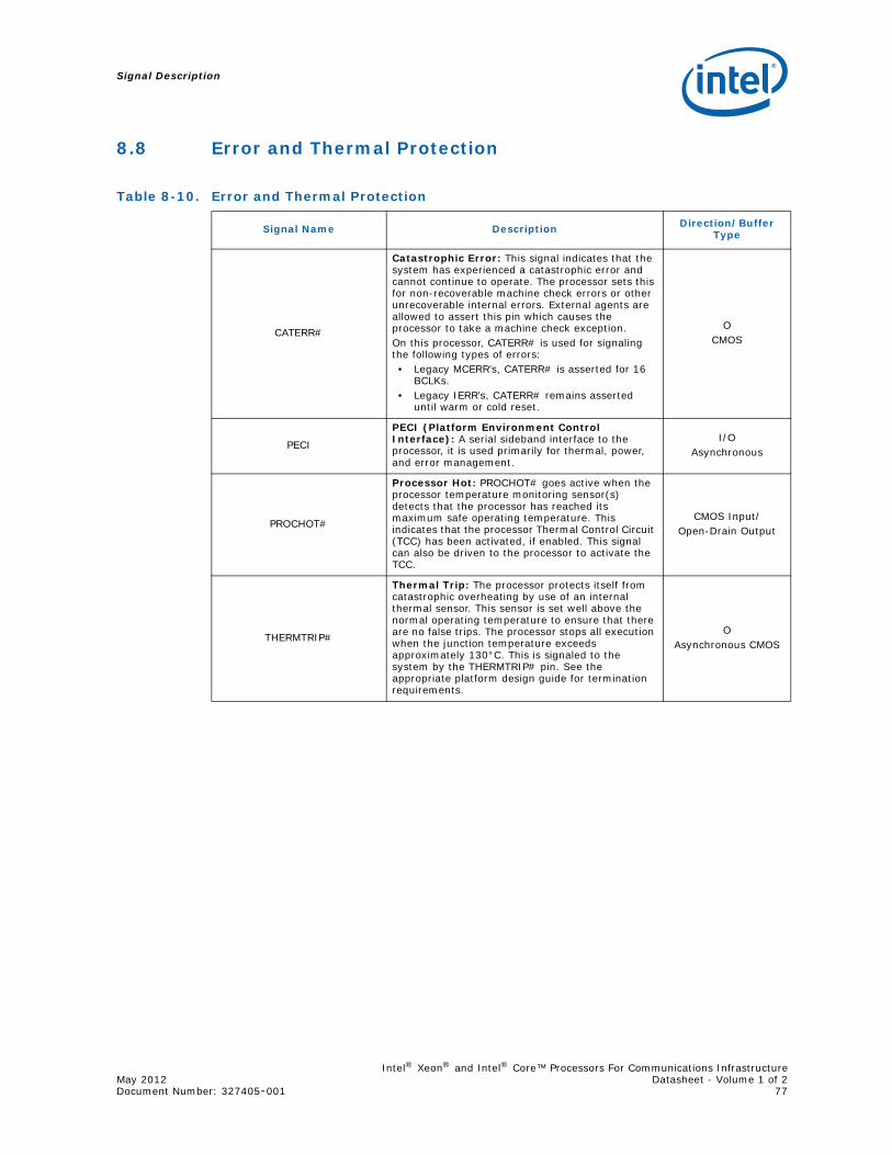
Signal Description
Intel® Xeon® and Intel® Core™ Processors For Communications InfrastructureMay 2012 Datasheet - Volume 1 of 2Document Number: 327405-001 77
8.8 Error and Thermal Protection
Table 8-10. Error and Thermal Protection
Signal Name Description Direction/Buffer Type
CATERR#
Catastrophic Error: This signal indicates that the system has experienced a catastrophic error and cannot continue to operate. The processor sets this for non-recoverable machine check errors or other unrecoverable internal errors. External agents are allowed to assert this pin which causes the processor to take a machine check exception.On this processor, CATERR# is used for signaling the following types of errors:• Legacy MCERR’s, CATERR# is asserted for 16
BCLKs.• Legacy IERR’s, CATERR# remains asserted
until warm or cold reset.
O CMOS
PECI
PECI (Platform Environment Control Interface): A serial sideband interface to the processor, it is used primarily for thermal, power, and error management.
I/OAsynchronous
PROCHOT#
Processor Hot: PROCHOT# goes active when the processor temperature monitoring sensor(s) detects that the processor has reached its maximum safe operating temperature. This indicates that the processor Thermal Control Circuit (TCC) has been activated, if enabled. This signal can also be driven to the processor to activate the TCC.
CMOS Input/Open-Drain Output
THERMTRIP#
Thermal Trip: The processor protects itself from catastrophic overheating by use of an internal thermal sensor. This sensor is set well above the normal operating temperature to ensure that there are no false trips. The processor stops all execution when the junction temperature exceeds approximately 130°C. This is signaled to the system by the THERMTRIP# pin. See the appropriate platform design guide for termination requirements.
OAsynchronous CMOS
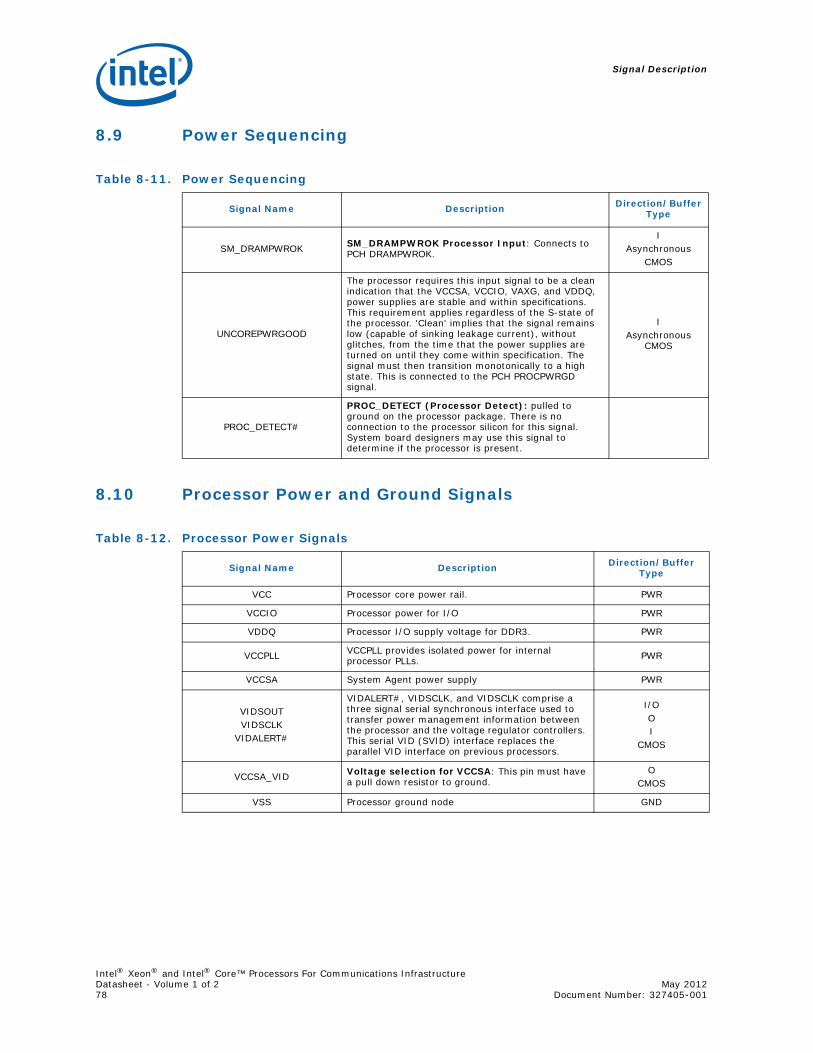
Signal Description
Intel® Xeon® and Intel® Core™ Processors For Communications InfrastructureDatasheet - Volume 1 of 2 May 201278 Document Number: 327405-001
8.9 Power Sequencing
8.10 Processor Power and Ground Signals
Table 8-11. Power Sequencing
Signal Name Description Direction/Buffer Type
SM_DRAMPWROK SM_DRAMPWROK Processor Input: Connects to PCH DRAMPWROK.
IAsynchronous
CMOS
UNCOREPWRGOOD
The processor requires this input signal to be a clean indication that the VCCSA, VCCIO, VAXG, and VDDQ, power supplies are stable and within specifications. This requirement applies regardless of the S-state of the processor. 'Clean' implies that the signal remains low (capable of sinking leakage current), without glitches, from the time that the power supplies are turned on until they come within specification. The signal must then transition monotonically to a high state. This is connected to the PCH PROCPWRGD signal.
IAsynchronous
CMOS
PROC_DETECT#
PROC_DETECT (Processor Detect): pulled to ground on the processor package. There is no connection to the processor silicon for this signal. System board designers may use this signal to determine if the processor is present.
Table 8-12. Processor Power Signals
Signal Name Description Direction/Buffer Type
VCC Processor core power rail. PWR
VCCIO Processor power for I/O PWR
VDDQ Processor I/O supply voltage for DDR3. PWR
VCCPLL VCCPLL provides isolated power for internal processor PLLs. PWR
VCCSA System Agent power supply PWR
VIDSOUTVIDSCLK
VIDALERT#
VIDALERT#, VIDSCLK, and VIDSCLK comprise a three signal serial synchronous interface used to transfer power management information between the processor and the voltage regulator controllers. This serial VID (SVID) interface replaces the parallel VID interface on previous processors.
I/OOI
CMOS
VCCSA_VID Voltage selection for VCCSA: This pin must have a pull down resistor to ground.
OCMOS
VSS Processor ground node GND
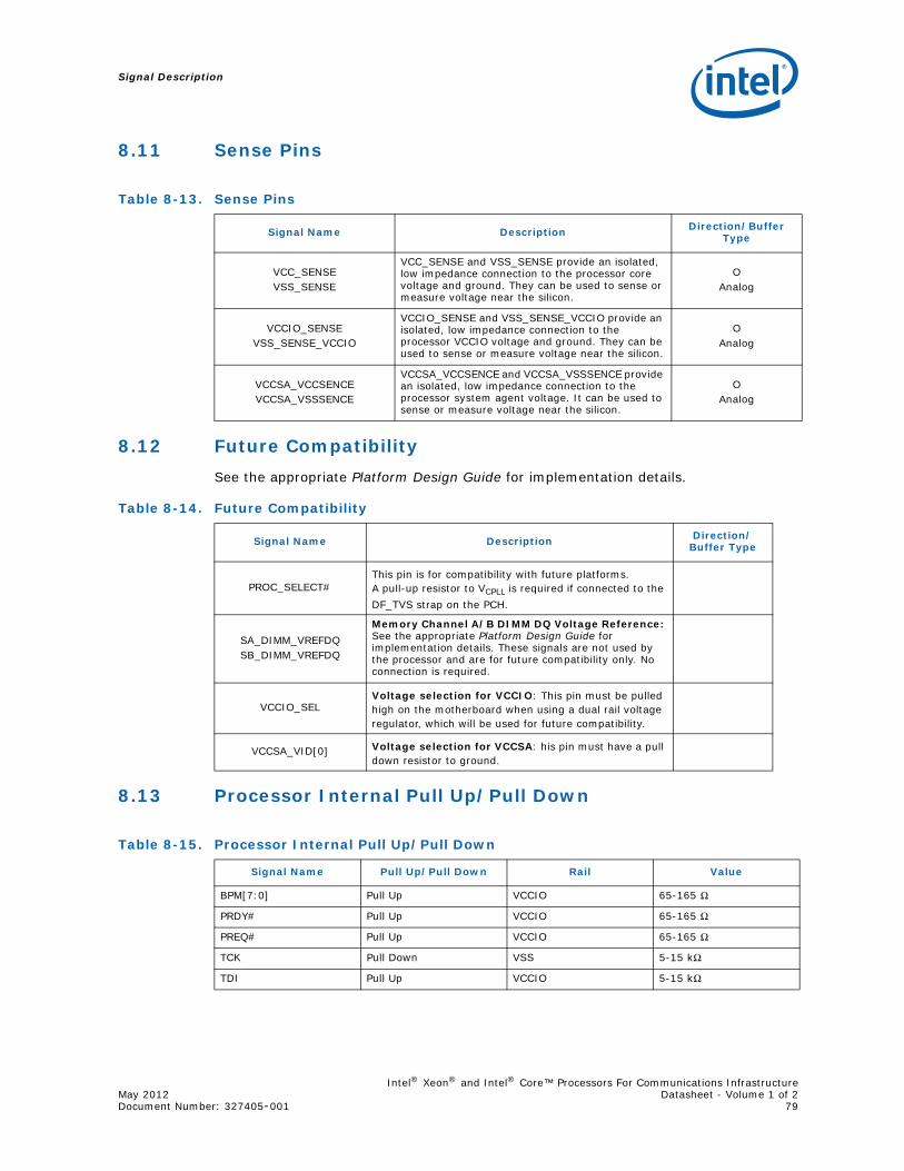
Signal Description
Intel® Xeon® and Intel® Core™ Processors For Communications InfrastructureMay 2012 Datasheet - Volume 1 of 2Document Number: 327405-001 79
8.11 Sense Pins
8.12 Future CompatibilitySee the appropriate Platform Design Guide for implementation details.
8.13 Processor Internal Pull Up/Pull Down
Table 8-13. Sense Pins
Signal Name Description Direction/Buffer Type
VCC_SENSEVSS_SENSE
VCC_SENSE and VSS_SENSE provide an isolated, low impedance connection to the processor core voltage and ground. They can be used to sense or measure voltage near the silicon.
OAnalog
VCCIO_SENSEVSS_SENSE_VCCIO
VCCIO_SENSE and VSS_SENSE_VCCIO provide an isolated, low impedance connection to the processor VCCIO voltage and ground. They can be used to sense or measure voltage near the silicon.
OAnalog
VCCSA_VCCSENCEVCCSA_VSSSENCE
VCCSA_VCCSENCE and VCCSA_VSSSENCE provide an isolated, low impedance connection to the processor system agent voltage. It can be used to sense or measure voltage near the silicon.
OAnalog
Table 8-14. Future Compatibility
Signal Name Description Direction/Buffer Type
PROC_SELECT#This pin is for compatibility with future platforms. A pull-up resistor to VCPLL is required if connected to the DF_TVS strap on the PCH.
SA_DIMM_VREFDQSB_DIMM_VREFDQ
Memory Channel A/B DIMM DQ Voltage Reference: See the appropriate Platform Design Guide for implementation details. These signals are not used by the processor and are for future compatibility only. No connection is required.
VCCIO_SELVoltage selection for VCCIO: This pin must be pulled high on the motherboard when using a dual rail voltage regulator, which will be used for future compatibility.
VCCSA_VID[0] Voltage selection for VCCSA: his pin must have a pull down resistor to ground.
Table 8-15. Processor Internal Pull Up/Pull Down
Signal Name Pull Up/Pull Down Rail Value
BPM[7:0] Pull Up VCCIO 65-165 Ω
PRDY# Pull Up VCCIO 65-165 Ω
PREQ# Pull Up VCCIO 65-165 Ω
TCK Pull Down VSS 5-15 kΩ
TDI Pull Up VCCIO 5-15 kΩ
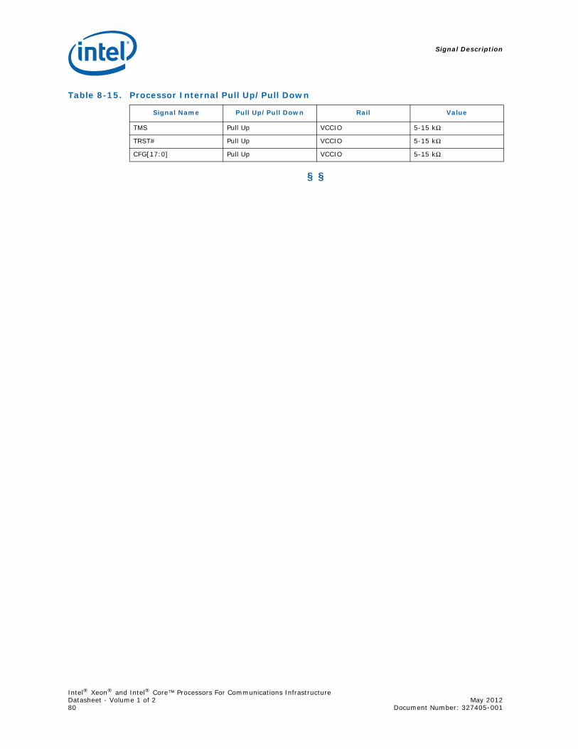
Signal Description
Intel® Xeon® and Intel® Core™ Processors For Communications InfrastructureDatasheet - Volume 1 of 2 May 201280 Document Number: 327405-001
§ §
TMS Pull Up VCCIO 5-15 kΩ
TRST# Pull Up VCCIO 5-15 kΩ
CFG[17:0] Pull Up VCCIO 5-15 kΩ
Table 8-15. Processor Internal Pull Up/Pull Down
Signal Name Pull Up/Pull Down Rail Value
Electrical Specifications
Intel® Xeon® and Intel® Core™ Processors For Communications InfrastructureMay 2012 Datasheet - Volume 1 of 2Document Number: 327405-001 81
9.0 Electrical Specifications
9.1 Power and Ground PinsThe processor has VCC, VCCIO, VDDQ, VCCPLL, VCCSA and VSS (ground) inputs for on-chip power distribution. All power pins must be connected to their respective processor power planes, while all VSS pins must be connected to the system ground plane. Use of multiple power and ground planes is recommended to reduce I*R drop. The VCC pins must be supplied with the voltage determined by the processor Serial Voltage IDentification (SVID) interface. Table 9-1 specifies the voltage level for the various VIDs.
9.2 Decoupling GuidelinesDue to its large number of transistors and high internal clock speeds, the processor is capable of generating large current swings between low- and full-power states. To keep voltages within specification, output decoupling must be properly designed.
Caution: Design the board to ensure that the voltage provided to the processor remains within the specifications listed in Table 9-5. Failure to do so can result in timing violations or reduced lifetime of the processor.
9.2.1 Voltage Rail Decoupling
The voltage regulator solution must:• Provide sufficient decoupling to compensate for large current swings generated
during different power mode transitions.• Provide low parasitic resistance from the regulator to the socket.• Meet voltage and current specifications as defined in Table 9-5.
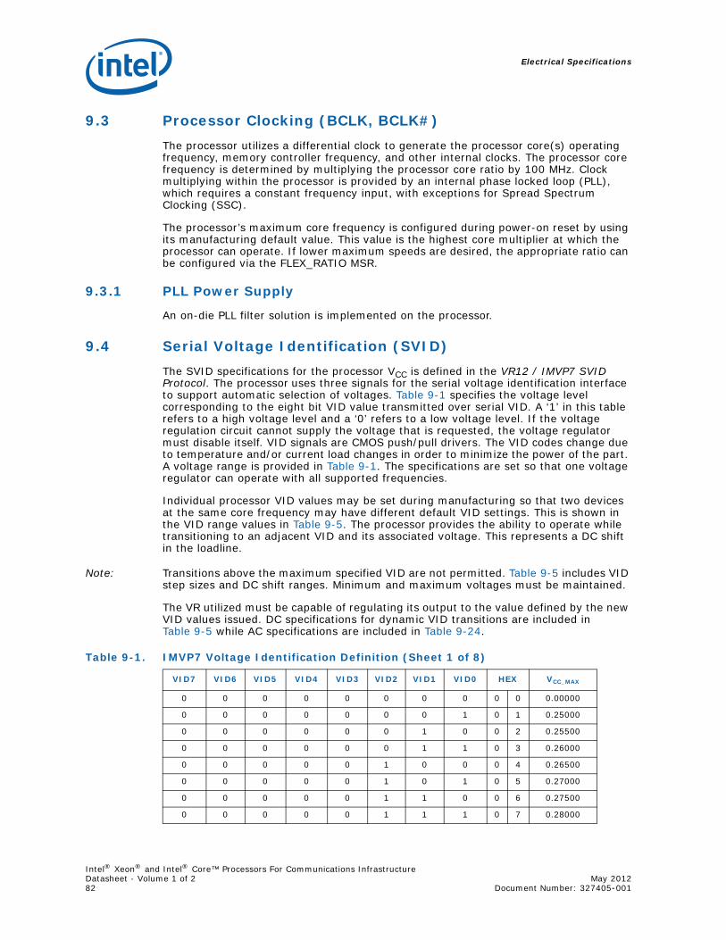
Electrical Specifications
Intel® Xeon® and Intel® Core™ Processors For Communications InfrastructureDatasheet - Volume 1 of 2 May 201282 Document Number: 327405-001
9.3 Processor Clocking (BCLK, BCLK#)The processor utilizes a differential clock to generate the processor core(s) operating frequency, memory controller frequency, and other internal clocks. The processor core frequency is determined by multiplying the processor core ratio by 100 MHz. Clock multiplying within the processor is provided by an internal phase locked loop (PLL), which requires a constant frequency input, with exceptions for Spread Spectrum Clocking (SSC).
The processor’s maximum core frequency is configured during power-on reset by using its manufacturing default value. This value is the highest core multiplier at which the processor can operate. If lower maximum speeds are desired, the appropriate ratio can be configured via the FLEX_RATIO MSR.
9.3.1 PLL Power Supply
An on-die PLL filter solution is implemented on the processor.
9.4 Serial Voltage Identification (SVID)The SVID specifications for the processor VCC is defined in the VR12 / IMVP7 SVID Protocol. The processor uses three signals for the serial voltage identification interface to support automatic selection of voltages. Table 9-1 specifies the voltage level corresponding to the eight bit VID value transmitted over serial VID. A ‘1’ in this table refers to a high voltage level and a ‘0’ refers to a low voltage level. If the voltage regulation circuit cannot supply the voltage that is requested, the voltage regulator must disable itself. VID signals are CMOS push/pull drivers. The VID codes change due to temperature and/or current load changes in order to minimize the power of the part. A voltage range is provided in Table 9-1. The specifications are set so that one voltage regulator can operate with all supported frequencies.
Individual processor VID values may be set during manufacturing so that two devices at the same core frequency may have different default VID settings. This is shown in the VID range values in Table 9-5. The processor provides the ability to operate while transitioning to an adjacent VID and its associated voltage. This represents a DC shift in the loadline.
Note: Transitions above the maximum specified VID are not permitted. Table 9-5 includes VID step sizes and DC shift ranges. Minimum and maximum voltages must be maintained.
The VR utilized must be capable of regulating its output to the value defined by the new VID values issued. DC specifications for dynamic VID transitions are included in Table 9-5 while AC specifications are included in Table 9-24.
Table 9-1. IMVP7 Voltage Identification Definition (Sheet 1 of 8)
VID7 VID6 VID5 VID4 VID3 VID2 VID1 VID0 HEX VCC_MAX
0 0 0 0 0 0 0 0 0 0 0.00000
0 0 0 0 0 0 0 1 0 1 0.25000
0 0 0 0 0 0 1 0 0 2 0.25500
0 0 0 0 0 0 1 1 0 3 0.26000
0 0 0 0 0 1 0 0 0 4 0.26500
0 0 0 0 0 1 0 1 0 5 0.27000
0 0 0 0 0 1 1 0 0 6 0.27500
0 0 0 0 0 1 1 1 0 7 0.28000

Electrical Specifications
Intel® Xeon® and Intel® Core™ Processors For Communications InfrastructureMay 2012 Datasheet - Volume 1 of 2Document Number: 327405-001 83
0 0 0 0 1 0 0 0 0 8 0.28500
0 0 0 0 1 0 0 1 0 9 0.29000
0 0 0 0 1 0 1 0 0 A 0.29500
0 0 0 0 1 0 1 1 0 B 0.30000
0 0 0 0 1 1 0 0 0 C 0.30500
0 0 0 0 1 1 0 1 0 D 0.31000
0 0 0 0 1 1 1 0 0 E 0.31500
0 0 0 0 1 1 1 1 0 F 0.32000
0 0 0 1 0 0 0 0 1 0 0.32500
0 0 0 1 0 0 0 1 1 1 0.33000
0 0 0 1 0 0 1 0 1 2 0.33500
0 0 0 1 0 0 1 1 1 3 0.34000
0 0 0 1 0 1 0 0 1 4 0.34500
0 0 0 1 0 1 0 1 1 5 0.35000
0 0 0 1 0 1 1 0 1 6 0.35500
0 0 0 1 0 1 1 1 1 7 0.36000
0 0 0 1 1 0 0 0 1 8 0.36500
0 0 0 1 1 0 0 1 1 9 0.37000
0 0 0 1 1 0 1 0 1 A 0.37500
0 0 0 1 1 0 1 1 1 B 0.38000
0 0 0 1 1 1 0 0 1 C 0.38500
0 0 0 1 1 1 0 1 1 D 0.39000
0 0 0 1 1 1 1 0 1 E 0.39500
0 0 0 1 1 1 1 1 1 F 0.40000
0 0 1 0 0 0 0 0 2 0 0.40500
0 0 1 0 0 0 0 1 2 1 0.41000
0 0 1 0 0 0 1 0 2 2 0.41500
0 0 1 0 0 0 1 1 2 3 0.42000
0 0 1 0 0 1 0 0 2 4 0.42500
0 0 1 0 0 1 0 1 2 5 0.43000
0 0 1 0 0 1 1 0 2 6 0.43500
0 0 1 0 0 1 1 1 2 7 0.44000
0 0 1 0 1 0 0 0 2 8 0.44500
0 0 1 0 1 0 0 1 2 9 0.45000
0 0 1 0 1 0 1 0 2 A 0.45500
0 0 1 0 1 0 1 1 2 B 0.46000
0 0 1 0 1 1 0 0 2 C 0.46500
0 0 1 0 1 1 0 1 2 D 0.47000
0 0 1 0 1 1 1 0 2 E 0.47500
0 0 1 0 1 1 1 1 2 F 0.48000
Table 9-1. IMVP7 Voltage Identification Definition (Sheet 2 of 8)
VID7 VID6 VID5 VID4 VID3 VID2 VID1 VID0 HEX VCC_MAX

Electrical Specifications
Intel® Xeon® and Intel® Core™ Processors For Communications InfrastructureDatasheet - Volume 1 of 2 May 201284 Document Number: 327405-001
0 0 1 1 0 0 0 0 3 0 0.48500
0 0 1 1 0 0 0 1 3 1 0.49000
0 0 1 1 0 0 1 0 3 2 0.49500
0 0 1 1 0 0 1 1 3 3 0.50000
0 0 1 1 0 1 0 0 3 4 0.50500
0 0 1 1 0 1 0 1 3 5 0.51000
0 0 1 1 0 1 1 0 3 6 0.51500
0 0 1 1 0 1 1 1 3 7 0.52000
0 0 1 1 1 0 0 0 3 8 0.52500
0 0 1 1 1 0 0 1 3 9 0.53000
0 0 1 1 1 0 1 0 3 A 0.53500
0 0 1 1 1 0 1 1 3 B 0.54000
0 0 1 1 1 1 0 0 3 C 0.54500
0 0 1 1 1 1 0 1 3 D 0.55000
0 0 1 1 1 1 1 0 3 E 0.55500
0 0 1 1 1 1 1 1 3 F 0.56000
0 1 0 0 0 0 0 0 4 0 0.56500
0 1 0 0 0 0 0 1 4 1 0.57000
0 1 0 0 0 0 1 0 4 2 0.57500
0 1 0 0 0 0 1 1 4 3 0.58000
0 1 0 0 0 1 0 0 4 4 0.58500
0 1 0 0 0 1 0 1 4 5 0.59000
0 1 0 0 0 1 1 0 4 6 0.59500
0 1 0 0 0 1 1 1 4 7 0.60000
0 1 0 0 1 0 0 0 4 8 0.60500
0 1 0 0 1 0 0 1 4 9 0.61000
0 1 0 0 1 0 1 0 4 A 0.61500
0 1 0 0 1 0 1 1 4 B 0.62000
0 1 0 0 1 1 0 0 4 C 0.62500
0 1 0 0 1 1 0 1 4 D 0.63000
0 1 0 0 1 1 1 0 4 E 0.63500
0 1 0 0 1 1 1 1 4 F 0.64000
0 1 0 1 0 0 0 0 5 0 0.64500
0 1 0 1 0 0 0 1 5 1 0.65000
0 1 0 1 0 0 1 0 5 2 0.65500
0 1 0 1 0 0 1 1 5 3 0.66000
0 1 0 1 0 1 0 0 5 4 0.66500
0 1 0 1 0 1 0 1 5 5 0.67000
0 1 0 1 0 1 1 0 5 6 0.67500
0 1 0 1 0 1 1 1 5 7 0.68000
Table 9-1. IMVP7 Voltage Identification Definition (Sheet 3 of 8)
VID7 VID6 VID5 VID4 VID3 VID2 VID1 VID0 HEX VCC_MAX
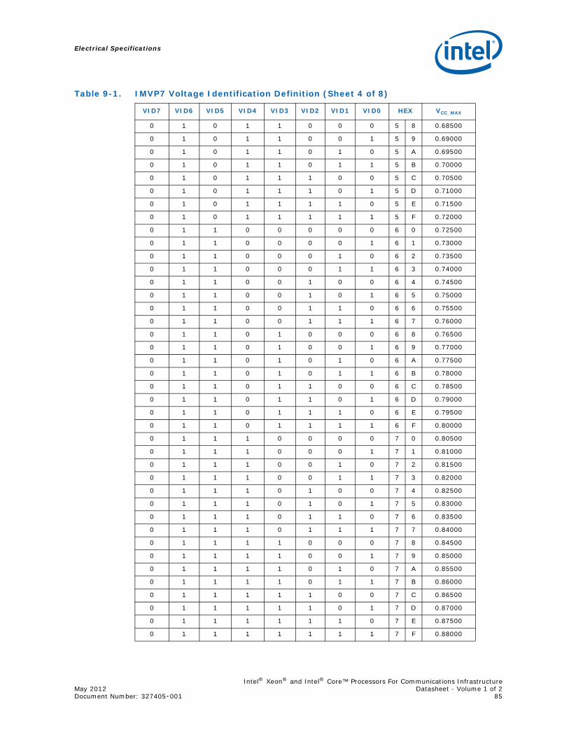
Electrical Specifications
Intel® Xeon® and Intel® Core™ Processors For Communications InfrastructureMay 2012 Datasheet - Volume 1 of 2Document Number: 327405-001 85
0 1 0 1 1 0 0 0 5 8 0.68500
0 1 0 1 1 0 0 1 5 9 0.69000
0 1 0 1 1 0 1 0 5 A 0.69500
0 1 0 1 1 0 1 1 5 B 0.70000
0 1 0 1 1 1 0 0 5 C 0.70500
0 1 0 1 1 1 0 1 5 D 0.71000
0 1 0 1 1 1 1 0 5 E 0.71500
0 1 0 1 1 1 1 1 5 F 0.72000
0 1 1 0 0 0 0 0 6 0 0.72500
0 1 1 0 0 0 0 1 6 1 0.73000
0 1 1 0 0 0 1 0 6 2 0.73500
0 1 1 0 0 0 1 1 6 3 0.74000
0 1 1 0 0 1 0 0 6 4 0.74500
0 1 1 0 0 1 0 1 6 5 0.75000
0 1 1 0 0 1 1 0 6 6 0.75500
0 1 1 0 0 1 1 1 6 7 0.76000
0 1 1 0 1 0 0 0 6 8 0.76500
0 1 1 0 1 0 0 1 6 9 0.77000
0 1 1 0 1 0 1 0 6 A 0.77500
0 1 1 0 1 0 1 1 6 B 0.78000
0 1 1 0 1 1 0 0 6 C 0.78500
0 1 1 0 1 1 0 1 6 D 0.79000
0 1 1 0 1 1 1 0 6 E 0.79500
0 1 1 0 1 1 1 1 6 F 0.80000
0 1 1 1 0 0 0 0 7 0 0.80500
0 1 1 1 0 0 0 1 7 1 0.81000
0 1 1 1 0 0 1 0 7 2 0.81500
0 1 1 1 0 0 1 1 7 3 0.82000
0 1 1 1 0 1 0 0 7 4 0.82500
0 1 1 1 0 1 0 1 7 5 0.83000
0 1 1 1 0 1 1 0 7 6 0.83500
0 1 1 1 0 1 1 1 7 7 0.84000
0 1 1 1 1 0 0 0 7 8 0.84500
0 1 1 1 1 0 0 1 7 9 0.85000
0 1 1 1 1 0 1 0 7 A 0.85500
0 1 1 1 1 0 1 1 7 B 0.86000
0 1 1 1 1 1 0 0 7 C 0.86500
0 1 1 1 1 1 0 1 7 D 0.87000
0 1 1 1 1 1 1 0 7 E 0.87500
0 1 1 1 1 1 1 1 7 F 0.88000
Table 9-1. IMVP7 Voltage Identification Definition (Sheet 4 of 8)
VID7 VID6 VID5 VID4 VID3 VID2 VID1 VID0 HEX VCC_MAX
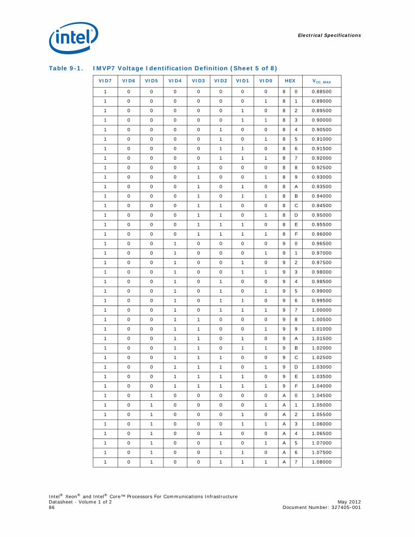
Electrical Specifications
Intel® Xeon® and Intel® Core™ Processors For Communications InfrastructureDatasheet - Volume 1 of 2 May 201286 Document Number: 327405-001
1 0 0 0 0 0 0 0 8 0 0.88500
1 0 0 0 0 0 0 1 8 1 0.89000
1 0 0 0 0 0 1 0 8 2 0.89500
1 0 0 0 0 0 1 1 8 3 0.90000
1 0 0 0 0 1 0 0 8 4 0.90500
1 0 0 0 0 1 0 1 8 5 0.91000
1 0 0 0 0 1 1 0 8 6 0.91500
1 0 0 0 0 1 1 1 8 7 0.92000
1 0 0 0 1 0 0 0 8 8 0.92500
1 0 0 0 1 0 0 1 8 9 0.93000
1 0 0 0 1 0 1 0 8 A 0.93500
1 0 0 0 1 0 1 1 8 B 0.94000
1 0 0 0 1 1 0 0 8 C 0.94500
1 0 0 0 1 1 0 1 8 D 0.95000
1 0 0 0 1 1 1 0 8 E 0.95500
1 0 0 0 1 1 1 1 8 F 0.96000
1 0 0 1 0 0 0 0 9 0 0.96500
1 0 0 1 0 0 0 1 9 1 0.97000
1 0 0 1 0 0 1 0 9 2 0.97500
1 0 0 1 0 0 1 1 9 3 0.98000
1 0 0 1 0 1 0 0 9 4 0.98500
1 0 0 1 0 1 0 1 9 5 0.99000
1 0 0 1 0 1 1 0 9 6 0.99500
1 0 0 1 0 1 1 1 9 7 1.00000
1 0 0 1 1 0 0 0 9 8 1.00500
1 0 0 1 1 0 0 1 9 9 1.01000
1 0 0 1 1 0 1 0 9 A 1.01500
1 0 0 1 1 0 1 1 9 B 1.02000
1 0 0 1 1 1 0 0 9 C 1.02500
1 0 0 1 1 1 0 1 9 D 1.03000
1 0 0 1 1 1 1 0 9 E 1.03500
1 0 0 1 1 1 1 1 9 F 1.04000
1 0 1 0 0 0 0 0 A 0 1.04500
1 0 1 0 0 0 0 1 A 1 1.05000
1 0 1 0 0 0 1 0 A 2 1.05500
1 0 1 0 0 0 1 1 A 3 1.06000
1 0 1 0 0 1 0 0 A 4 1.06500
1 0 1 0 0 1 0 1 A 5 1.07000
1 0 1 0 0 1 1 0 A 6 1.07500
1 0 1 0 0 1 1 1 A 7 1.08000
Table 9-1. IMVP7 Voltage Identification Definition (Sheet 5 of 8)
VID7 VID6 VID5 VID4 VID3 VID2 VID1 VID0 HEX VCC_MAX

Electrical Specifications
Intel® Xeon® and Intel® Core™ Processors For Communications InfrastructureMay 2012 Datasheet - Volume 1 of 2Document Number: 327405-001 87
1 0 1 0 1 0 0 0 A 8 1.08500
1 0 1 0 1 0 0 1 A 9 1.09000
1 0 1 0 1 0 1 0 A A 1.09500
1 0 1 0 1 0 1 1 A B 1.10000
1 0 1 0 1 1 0 0 A C 1.10500
1 0 1 0 1 1 0 1 A D 1.11000
1 0 1 0 1 1 1 0 A E 1.11500
1 0 1 0 1 1 1 1 A F 1.12000
1 0 1 1 0 0 0 0 B 0 1.12500
1 0 1 1 0 0 0 1 B 1 1.13000
1 0 1 1 0 0 1 0 B 2 1.13500
1 0 1 1 0 0 1 1 B 3 1.14000
1 0 1 1 0 1 0 0 B 4 1.14500
1 0 1 1 0 1 0 1 B 5 1.15000
1 0 1 1 0 1 1 0 B 6 1.15500
1 0 1 1 0 1 1 1 B 7 1.16000
1 0 1 1 1 0 0 0 B 8 1.16500
1 0 1 1 1 0 0 1 B 9 1.17000
1 0 1 1 1 0 1 0 B A 1.17500
1 0 1 1 1 0 1 1 B B 1.18000
1 0 1 1 1 1 0 0 B C 1.18500
1 0 1 1 1 1 0 1 B D 1.19000
1 0 1 1 1 1 1 0 B E 1.19500
1 0 1 1 1 1 1 1 B F 1.20000
1 1 0 0 0 0 0 0 C 0 1.20500
1 1 0 0 0 0 0 1 C 1 1.21000
1 1 0 0 0 0 1 0 C 2 1.21500
1 1 0 0 0 0 1 1 C 3 1.22000
1 1 0 0 0 1 0 0 C 4 1.22500
1 1 0 0 0 1 0 1 C 5 1.23000
1 1 0 0 0 1 1 0 C 6 1.23500
1 1 0 0 0 1 1 1 C 7 1.24000
1 1 0 0 1 0 0 0 C 8 1.24500
1 1 0 0 1 0 0 1 C 9 1.25000
1 1 0 0 1 0 1 0 C A 1.25500
1 1 0 0 1 0 1 1 C B 1.26000
1 1 0 0 1 1 0 0 C C 1.26500
1 1 0 0 1 1 0 1 C D 1.27000
1 1 0 0 1 1 1 0 C E 1.27500
1 1 0 0 1 1 1 1 C F 1.28000
Table 9-1. IMVP7 Voltage Identification Definition (Sheet 6 of 8)
VID7 VID6 VID5 VID4 VID3 VID2 VID1 VID0 HEX VCC_MAX
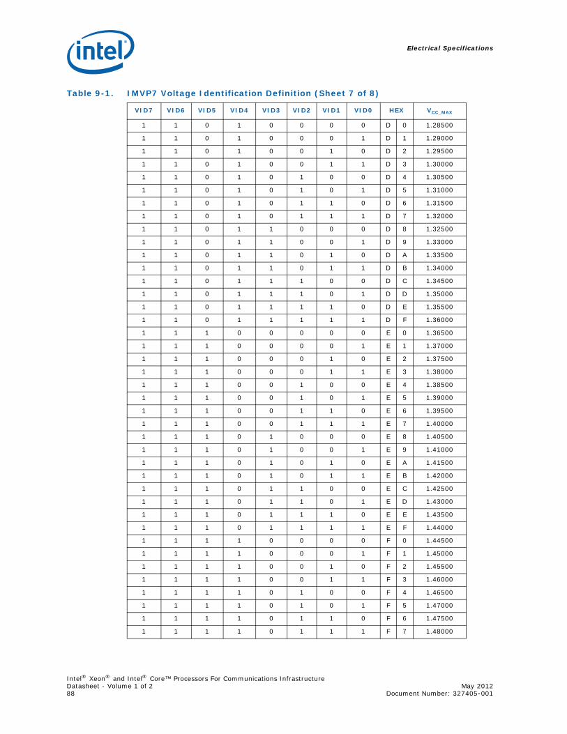
Electrical Specifications
Intel® Xeon® and Intel® Core™ Processors For Communications InfrastructureDatasheet - Volume 1 of 2 May 201288 Document Number: 327405-001
1 1 0 1 0 0 0 0 D 0 1.28500
1 1 0 1 0 0 0 1 D 1 1.29000
1 1 0 1 0 0 1 0 D 2 1.29500
1 1 0 1 0 0 1 1 D 3 1.30000
1 1 0 1 0 1 0 0 D 4 1.30500
1 1 0 1 0 1 0 1 D 5 1.31000
1 1 0 1 0 1 1 0 D 6 1.31500
1 1 0 1 0 1 1 1 D 7 1.32000
1 1 0 1 1 0 0 0 D 8 1.32500
1 1 0 1 1 0 0 1 D 9 1.33000
1 1 0 1 1 0 1 0 D A 1.33500
1 1 0 1 1 0 1 1 D B 1.34000
1 1 0 1 1 1 0 0 D C 1.34500
1 1 0 1 1 1 0 1 D D 1.35000
1 1 0 1 1 1 1 0 D E 1.35500
1 1 0 1 1 1 1 1 D F 1.36000
1 1 1 0 0 0 0 0 E 0 1.36500
1 1 1 0 0 0 0 1 E 1 1.37000
1 1 1 0 0 0 1 0 E 2 1.37500
1 1 1 0 0 0 1 1 E 3 1.38000
1 1 1 0 0 1 0 0 E 4 1.38500
1 1 1 0 0 1 0 1 E 5 1.39000
1 1 1 0 0 1 1 0 E 6 1.39500
1 1 1 0 0 1 1 1 E 7 1.40000
1 1 1 0 1 0 0 0 E 8 1.40500
1 1 1 0 1 0 0 1 E 9 1.41000
1 1 1 0 1 0 1 0 E A 1.41500
1 1 1 0 1 0 1 1 E B 1.42000
1 1 1 0 1 1 0 0 E C 1.42500
1 1 1 0 1 1 0 1 E D 1.43000
1 1 1 0 1 1 1 0 E E 1.43500
1 1 1 0 1 1 1 1 E F 1.44000
1 1 1 1 0 0 0 0 F 0 1.44500
1 1 1 1 0 0 0 1 F 1 1.45000
1 1 1 1 0 0 1 0 F 2 1.45500
1 1 1 1 0 0 1 1 F 3 1.46000
1 1 1 1 0 1 0 0 F 4 1.46500
1 1 1 1 0 1 0 1 F 5 1.47000
1 1 1 1 0 1 1 0 F 6 1.47500
1 1 1 1 0 1 1 1 F 7 1.48000
Table 9-1. IMVP7 Voltage Identification Definition (Sheet 7 of 8)
VID7 VID6 VID5 VID4 VID3 VID2 VID1 VID0 HEX VCC_MAX
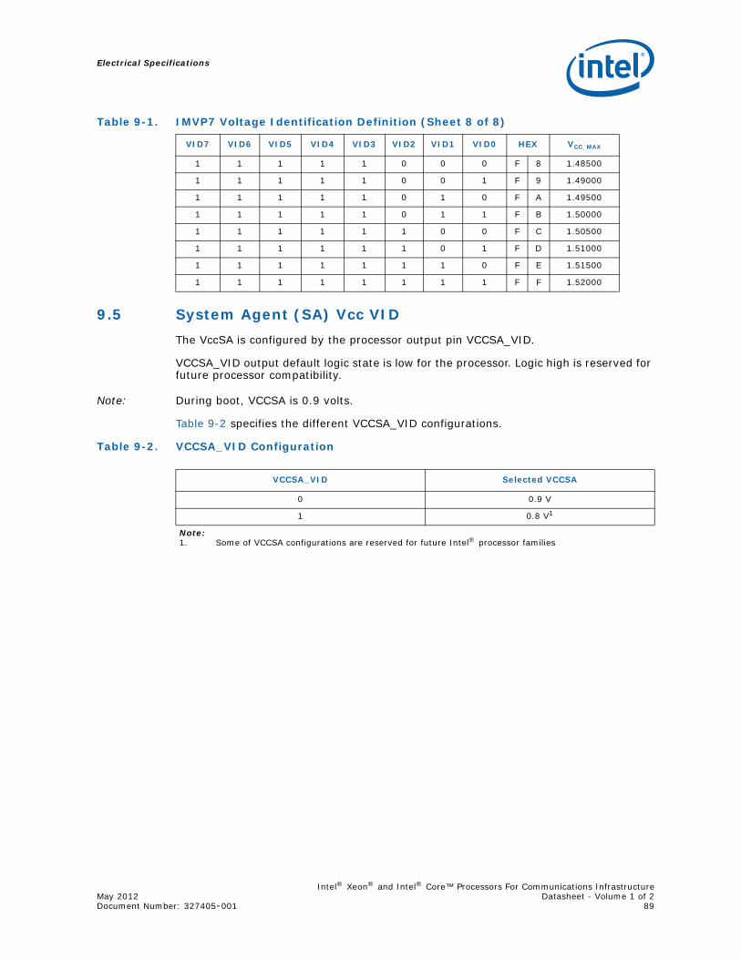
Electrical Specifications
Intel® Xeon® and Intel® Core™ Processors For Communications InfrastructureMay 2012 Datasheet - Volume 1 of 2Document Number: 327405-001 89
9.5 System Agent (SA) Vcc VIDThe VccSA is configured by the processor output pin VCCSA_VID.
VCCSA_VID output default logic state is low for the processor. Logic high is reserved for future processor compatibility.
Note: During boot, VCCSA is 0.9 volts.
Table 9-2 specifies the different VCCSA_VID configurations.
Table 9-2. VCCSA_VID Configuration
1 1 1 1 1 0 0 0 F 8 1.48500
1 1 1 1 1 0 0 1 F 9 1.49000
1 1 1 1 1 0 1 0 F A 1.49500
1 1 1 1 1 0 1 1 F B 1.50000
1 1 1 1 1 1 0 0 F C 1.50500
1 1 1 1 1 1 0 1 F D 1.51000
1 1 1 1 1 1 1 0 F E 1.51500
1 1 1 1 1 1 1 1 F F 1.52000
Table 9-1. IMVP7 Voltage Identification Definition (Sheet 8 of 8)
VID7 VID6 VID5 VID4 VID3 VID2 VID1 VID0 HEX VCC_MAX
VCCSA_VID Selected VCCSA
0 0.9 V
1 0.8 V1
Note:1. Some of VCCSA configurations are reserved for future Intel® processor families
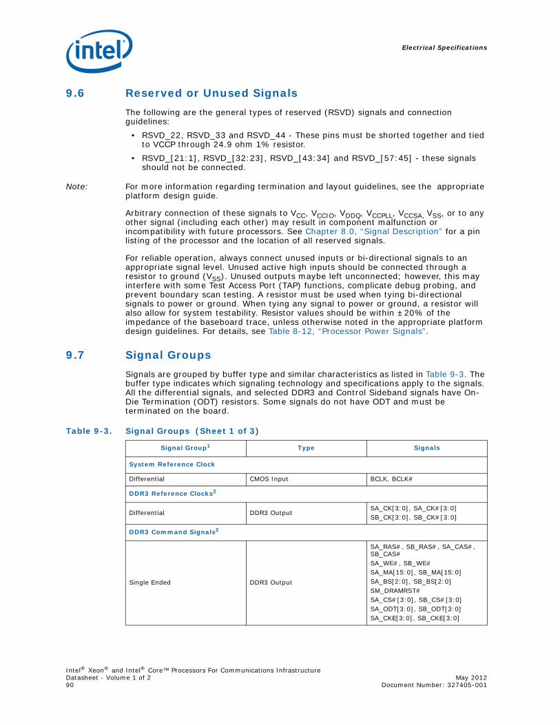
Electrical Specifications
Intel® Xeon® and Intel® Core™ Processors For Communications InfrastructureDatasheet - Volume 1 of 2 May 201290 Document Number: 327405-001
9.6 Reserved or Unused SignalsThe following are the general types of reserved (RSVD) signals and connection guidelines:
• RSVD_22, RSVD_33 and RSVD_44 - These pins must be shorted together and tied to VCCP through 24.9 ohm 1% resistor.
• RSVD_[21:1], RSVD_[32:23], RSVD_[43:34] and RSVD_[57:45] - these signals should not be connected.
Note: For more information regarding termination and layout guidelines, see the appropriate platform design guide.
Arbitrary connection of these signals to VCC, VCCIO, VDDQ, VCCPLL, VCCSA, VSS, or to any other signal (including each other) may result in component malfunction or incompatibility with future processors. See Chapter 8.0, “Signal Description” for a pin listing of the processor and the location of all reserved signals.
For reliable operation, always connect unused inputs or bi-directional signals to an appropriate signal level. Unused active high inputs should be connected through a resistor to ground (VSS). Unused outputs maybe left unconnected; however, this may interfere with some Test Access Port (TAP) functions, complicate debug probing, and prevent boundary scan testing. A resistor must be used when tying bi-directional signals to power or ground. When tying any signal to power or ground, a resistor will also allow for system testability. Resistor values should be within ±20% of the impedance of the baseboard trace, unless otherwise noted in the appropriate platform design guidelines. For details, see Table 8-12, “Processor Power Signals”.
9.7 Signal GroupsSignals are grouped by buffer type and similar characteristics as listed in Table 9-3. The buffer type indicates which signaling technology and specifications apply to the signals. All the differential signals, and selected DDR3 and Control Sideband signals have On-Die Termination (ODT) resistors. Some signals do not have ODT and must be terminated on the board.
Table 9-3. Signal Groups (Sheet 1 of 3)
Signal Group1 Type Signals
System Reference Clock
Differential CMOS Input BCLK, BCLK#
DDR3 Reference Clocks2
Differential DDR3 OutputSA_CK[3:0], SA_CK#[3:0]SB_CK[3:0], SB_CK#[3:0]
DDR3 Command Signals2
Single Ended DDR3 Output
SA_RAS#, SB_RAS#, SA_CAS#, SB_CAS#SA_WE#, SB_WE#SA_MA[15:0], SB_MA[15:0]SA_BS[2:0], SB_BS[2:0]SM_DRAMRST#SA_CS#[3:0], SB_CS#[3:0]SA_ODT[3:0], SB_ODT[3:0]SA_CKE[3:0], SB_CKE[3:0]
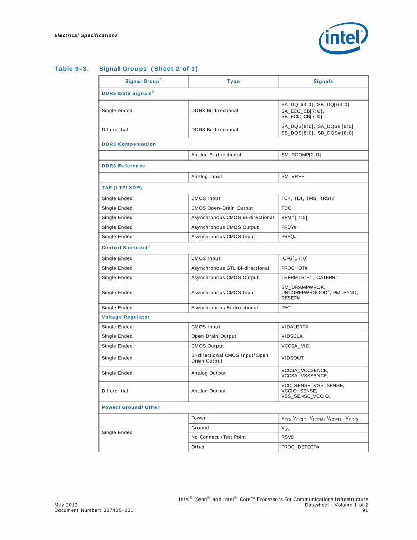
Electrical Specifications
Intel® Xeon® and Intel® Core™ Processors For Communications InfrastructureMay 2012 Datasheet - Volume 1 of 2Document Number: 327405-001 91
DDR3 Data Signals2
Single ended DDR3 Bi-directionalSA_DQ[63:0], SB_DQ[63:0]SA_ECC_CB[7:0], SB_ECC_CB[7:0]
Differential DDR3 Bi-directionalSA_DQS[8:0], SA_DQS#[8:0]SB_DQS[8:0], SB_DQS#[8:0]
DDR3 Compensation
Analog Bi-directional SM_RCOMP[2:0]
DDR3 Reference
Analog Input SM_VREF
TAP (ITP/XDP)
Single Ended CMOS Input TCK, TDI, TMS, TRST#
Single Ended CMOS Open-Drain Output TDO
Single Ended Asynchronous CMOS Bi-directional BPM#[7:0]
Single Ended Asynchronous CMOS Output PRDY#
Single Ended Asynchronous CMOS Input PREQ#
Control Sideband3
Single Ended CMOS Input CFG[17:0]
Single Ended Asynchronous GTL Bi-directional PROCHOT#
Single Ended Asynchronous CMOS Output THERMTRIP#, CATERR#
Single Ended Asynchronous CMOS InputSM_DRAMPWROK, UNCOREPWRGOOD4, PM_SYNC, RESET#
Single Ended Asynchronous Bi-directional PECI
Voltage Regulator
Single Ended CMOS Input VIDALERT#
Single Ended Open Drain Output VIDSCLK
Single Ended CMOS Output VCCSA_VID
Single Ended Bi-directional CMOS Input/Open Drain Output VIDSOUT
Single Ended Analog Output VCCSA_VCCSENCE, VCCSA_VSSSENCE,
Differential Analog OutputVCC_SENSE, VSS_SENSE, VCCIO_SENSE, VSS_SENSE_VCCIO,
Power/Ground/Other
Single Ended
Power VCC, VCCIO, VCCSA, VCCPLL, VDDQ
Ground VSS
No Connect /Test Point RSVD
Other PROC_DETECT#
Table 9-3. Signal Groups (Sheet 2 of 3)
Signal Group1 Type Signals
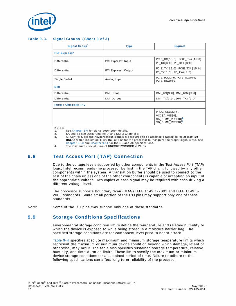
Electrical Specifications
Intel® Xeon® and Intel® Core™ Processors For Communications InfrastructureDatasheet - Volume 1 of 2 May 201292 Document Number: 327405-001
9.8 Test Access Port (TAP) ConnectionDue to the voltage levels supported by other components in the Test Access Port (TAP) logic, Intel recommends the processor be first in the TAP chain, followed by any other components within the system. A translation buffer should be used to connect to the rest of the chain unless one of the other components is capable of accepting an input of the appropriate voltage. Two copies of each signal may be required with each driving a different voltage level.
The processor supports Boundary Scan (JTAG) IEEE 1149.1-2001 and IEEE 1149.6-2003 standards. Some small portion of the I/O pins may support only one of these standards.
Note: Some of the I/O pins may support only one of these standards.
9.9 Storage Conditions SpecificationsEnvironmental storage condition limits define the temperature and relative humidity to which the device is exposed to while being stored in a moisture barrier bag. The specified storage conditions are for component level prior to board attach.
Table 9-4 specifies absolute maximum and minimum storage temperature limits which represent the maximum or minimum device condition beyond which damage, latent or otherwise, may occur. The table also specifies sustained storage temperature, relative humidity, and time-duration limits. These limits specify the maximum or minimum device storage conditions for a sustained period of time. Failure to adhere to the following specifications can affect long term reliability of the processor.
PCI Express*
Differential PCI Express* InputPCIE_RX[15:0], PCIE_RX#[15:0]PE_RX[3:0], PE_RX#[3:0]
Differential PCI Express* OutputPCIE_TX[15:0], PCIE_TX#[15:0]PE_TX[3:0], PE_TX#[3:0]
Single Ended Analog Input PCIE_ICOMP0, PCIE_ICOMPI, PCIE_RCOMP0
DMI
Differential DMI Input DMI_RX[3:0], DMI_RX#[3:0]
Differential DMI Output DMI_TX[3:0], DMI_TX#[3:0]
Future Compatibility
PROC_SELECT#,VCCSA_VID[0],SA_DIMM_VREFDQ2, SB_DIMM_VREFDQ2
Notes:1. See Chapter 8.0 for signal description details.2. SA and SB see DDR3 Channel A and DDR3 Channel B.3. All Control Sideband Asynchronous signals are required to be asserted/deasserted for at least 10
BCLKs with a maximum Trise/Tfall of 6 ns for the processor to recognize the proper signal state. See Chapter 9.10 and Chapter 9.11 for the DC and AC specifications.
4. The maximum rise/fall time of UNCOREPWRGOOD is 20 ns.
Table 9-3. Signal Groups (Sheet 3 of 3)
Signal Group1 Type Signals
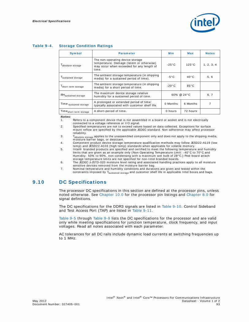
Electrical Specifications
Intel® Xeon® and Intel® Core™ Processors For Communications InfrastructureMay 2012 Datasheet - Volume 1 of 2Document Number: 327405-001 93
9.10 DC SpecificationsThe processor DC specifications in this section are defined at the processor pins, unless noted otherwise. See Chapter 10.0 for the processor pin listings and Chapter 8.0 for signal definitions.
The DC specifications for the DDR3 signals are listed in Table 9-10. Control Sideband and Test Access Port (TAP) are listed in Table 9-11.
Table 9-5 through Table 9-9 lists the DC specifications for the processor and are valid only while meeting specifications for junction temperature, clock frequency, and input voltages. Read all notes associated with each parameter.
AC tolerances for all DC rails include dynamic load currents at switching frequencies up to 1 MHz.
Table 9-4. Storage Condition Ratings
Symbol Parameter Min Max Notes
Tabsolute storage
The non-operating device storage temperature. Damage (latent or otherwise) may occur when exceeded for any length of time.
-25°C 125°C 1, 2, 3, 4
Tsustained storageThe ambient storage temperature (in shipping media) for a sustained period of time). -5°C 40°C 5, 6
Tshort term storageThe ambient storage temperature (in shipping media) for a short period of time. -20°C 85°C
RHsustained storageThe maximum device storage relative humidity for a sustained period of time. 60% @ 24°C 6, 7
Time sustained storageA prolonged or extended period of time; typically associated with customer shelf life. 0 Months 6 Months 7
Timeshort term storage A short-period of time. 0 hours 72 hours
Notes:1. Refers to a component device that is not assembled in a board or socket and is not electrically
connected to a voltage reference or I/O signal.2. Specified temperatures are not to exceed values based on data collected. Exceptions for surface
mount reflow are specified by the applicable JEDEC standard. Non-adherence may affect processor reliability.
3. Tabsolute storage applies to the unassembled component only and does not apply to the shipping media, moisture barrier bags, or desiccant.
4. Component product device storage temperature qualification methods may follow JESD22-A119 (low temp) and JESD22-A103 (high temp) standards when applicable for volatile memory.
5. Intel® branded products are specified and certified to meet the following temperature and humidity limits that are given as an example only (Non-Operating Temperature Limit: -40°C to 70°C and Humidity: 50% to 90%, non-condensing with a maximum wet bulb of 28°C.) Post board attach storage temperature limits are not specified for non-Intel branded boards.
6. The JEDEC J-JSTD-020 moisture level rating and associated handling practices apply to all moisture sensitive devices removed from the moisture barrier bag.
7. Nominal temperature and humidity conditions and durations are given and tested within the constraints imposed by Tsustained storage and customer shelf life in applicable Intel boxes and bags.
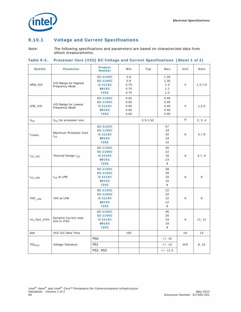
Electrical Specifications
Intel® Xeon® and Intel® Core™ Processors For Communications InfrastructureDatasheet - Volume 1 of 2 May 201294 Document Number: 327405-001
9.10.1 Voltage and Current Specifications
Note: The following specifications and parameters are based on characterized data from silicon measurements.
Table 9-5. Processor Core (VCC) DC Voltage and Current Specifications (Sheet 1 of 2)
Symbol Parameter Product Number Min Typ Max Unit Note
HFM_VID VID Range for Highest Frequency Mode
E3-1125CE3-1105Ci3 2115CB915C725C
0.80.80.750.700.70
1.351.351.31.21.2
V 1,2,7,9
LFM_VID VID Range for Lowest Frequency Mode
E3-1125CE3-1105Ci3 2115CB915C725C
0.650.650.650.650.65
0.950.950.900.900.90
V 1,2,9
VCC VCC for processor core 0.3-1.52 V 2, 3, 4
ICCMAXMaximum Processor Core ICC
E3-1125CE3-1105Ci3 2115CB915C725C
5733302310
A 5,7,9
ICC_TDC Thermal Design ICC
E3-1125CE3-1105Ci3 2115CB915C725C
352218138
A 6,7, 9
ICC_LFM ICC at LFM
E3-1125CE3-1105Ci3 2115CB915C725C
282815158
A 6
TDC_LFM TDC at LFM
E3-1125CE3-1105Ci3 2115CB915C725C
222212128
A 6
Icc_Dyn_VID1 Dynamic Current step size in VID1
E3-1125CE3-1105Ci3 2115CB915C725C
462624188
A 11, 12
didt VCC ICC Slew Time 150 nS 13
TOLVCC Voltage Tolerance
PS0 +/- 15
mV 8, 10PS1 +/- 12
PS2, PS3 +/- 11.5
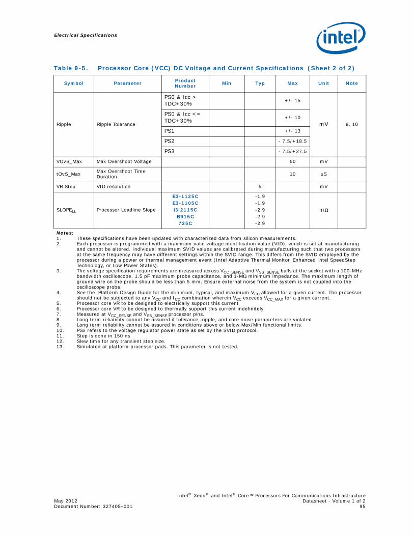
Electrical Specifications
Intel® Xeon® and Intel® Core™ Processors For Communications InfrastructureMay 2012 Datasheet - Volume 1 of 2Document Number: 327405-001 95
Ripple Ripple Tolerance
PS0 & Icc > TDC+30% +/- 15
mV 8, 10
PS0 & Icc <= TDC+30% +/- 10
PS1 +/- 13
PS2 - 7.5/+18.5
PS3 - 7.5/+27.5
VOvS_Max Max Overshoot Voltage 50 mV
tOvS_Max Max Overshoot Time Duration 10 uS
VR Step VID resolution 5 mV
SLOPELL Processor Loadline Slope
E3-1125CE3-1105Ci3 2115CB915C725C
-1.9-1.9-2.9-2.9-2.9
mΩ
Notes:1. These specifications have been updated with characterized data from silicon measurements.2. Each processor is programmed with a maximum valid voltage identification value (VID), which is set at manufacturing
and cannot be altered. Individual maximum SVID values are calibrated during manufacturing such that two processors at the same frequency may have different settings within the SVID range. This differs from the SVID employed by the processor during a power or thermal management event (Intel Adaptive Thermal Monitor, Enhanced Intel SpeedStep Technology, or Low Power States).
3. The voltage specification requirements are measured across VCC_SENSE and VSS_SENSE balls at the socket with a 100-MHz bandwidth oscilloscope, 1.5 pF maximum probe capacitance, and 1-MΩ minimum impedance. The maximum length of ground wire on the probe should be less than 5 mm. Ensure external noise from the system is not coupled into the oscilloscope probe.
4. See the Platform Design Guide for the minimum, typical, and maximum VCC allowed for a given current. The processor should not be subjected to any VCC and ICC combination wherein VCC exceeds VCC_MAX for a given current.
5. Processor core VR to be designed to electrically support this current6. Processor core VR to be designed to thermally support this current indefinitely.7. Measured at VCC_SENSE and VSS_SENSE processor pins.8. Long term reliability cannot be assured if tolerance, ripple, and core noise parameters are violated9. Long term reliability cannot be assured in conditions above or below Max/Min functional limits.10. PSx refers to the voltage regulator power state as set by the SVID protocol. 11. Step is done in 150 ns12. Slew time for any transient step size.13. Simulated at platform processor pads. This parameter is not tested.
Table 9-5. Processor Core (VCC) DC Voltage and Current Specifications (Sheet 2 of 2)
Symbol Parameter Product Number Min Typ Max Unit Note
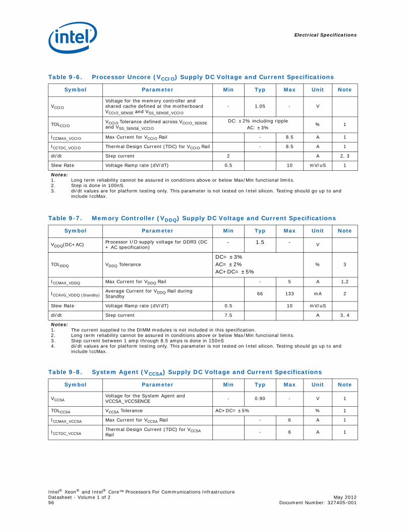
Electrical Specifications
Intel® Xeon® and Intel® Core™ Processors For Communications InfrastructureDatasheet - Volume 1 of 2 May 201296 Document Number: 327405-001
Table 9-6. Processor Uncore (VCCIO) Supply DC Voltage and Current Specifications
Symbol Parameter Min Typ Max Unit Note
VCCIO
Voltage for the memory controller and shared cache defined at the motherboard VCCIO_SENSE and VSS_SENSE_VCCIO
- 1.05 - V
TOLCCIOVCCIO Tolerance defined across VCCIO_SENSE and VSS_SENSE_VCCIO
DC: ±2% including rippleAC: ±3%
% 1
ICCMAX_VCCIO Max Current for VCCIO Rail - 8.5 A 1
ICCTDC_VCCIO Thermal Design Current (TDC) for VCCIO Rail - 8.5 A 1
di/dt Step current 2 A 2, 3
Slew Rate Voltage Ramp rate (dV/dT) 0.5 10 mV/uS 1
Notes:1. Long term reliability cannot be assured in conditions above or below Max/Min functional limits.2. Step is done in 100nS.3. di/dt values are for platform testing only. This parameter is not tested on Intel silicon. Testing should go up to and
include IccMax.
Table 9-7. Memory Controller (VDDQ) Supply DC Voltage and Current Specifications
Symbol Parameter Min Typ Max Unit Note
VDDQ(DC+AC) Processor I/O supply voltage for DDR3 (DC + AC specification)
- 1.5 - V
TOLDDQ VDDQ ToleranceDC= ±3%AC= ±2%AC+DC= ±5%
% 3
ICCMAX_VDDQ Max Current for VDDQ Rail - 5 A 1,2
ICCAVG_VDDQ (Standby)Average Current for VDDQ Rail during Standby 66 133 mA 2
Slew Rate Voltage Ramp rate (dV/dT) 0.5 10 mV/uS
di/dt Step current 7.5 A 3, 4
Notes:1. The current supplied to the DIMM modules is not included in this specification.2. Long term reliability cannot be assured in conditions above or below Max/Min functional limits.3. Step current between 1 amp through 8.5 amps is done in 150nS 4. di/dt values are for platform testing only. This parameter is not tested on Intel silicon. Testing should go up to and
include IccMax.
Table 9-8. System Agent (VCCSA) Supply DC Voltage and Current Specifications
Symbol Parameter Min Typ Max Unit Note
VCCSAVoltage for the System Agent and VCCSA_VCCSENCE - 0.90 - V 1
TOLCCSA VCCSA Tolerance AC+DC= ±5% % 1
ICCMAX_VCCSA Max Current for VCCSA Rail - 6 A 1
ICCTDC_VCCSAThermal Design Current (TDC) for VCCSA Rail - 6 A 1
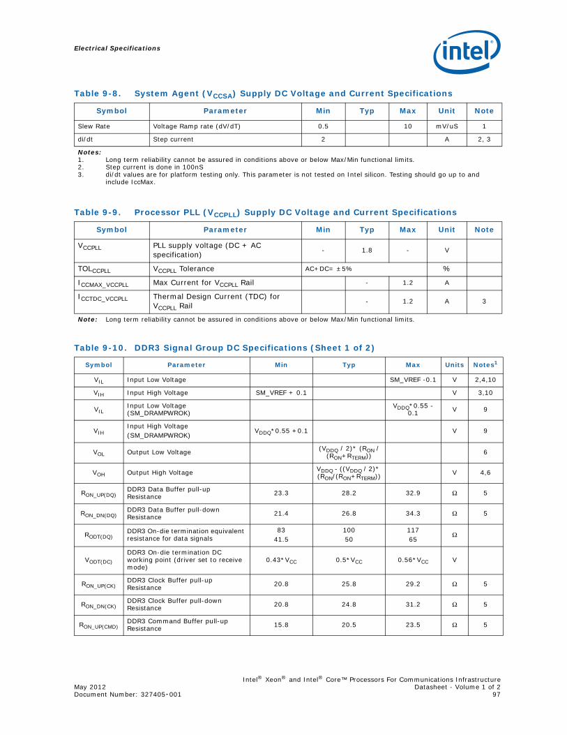
Electrical Specifications
Intel® Xeon® and Intel® Core™ Processors For Communications InfrastructureMay 2012 Datasheet - Volume 1 of 2Document Number: 327405-001 97
Slew Rate Voltage Ramp rate (dV/dT) 0.5 10 mV/uS 1
di/dt Step current 2 A 2, 3
Notes:1. Long term reliability cannot be assured in conditions above or below Max/Min functional limits.2. Step current is done in 100nS 3. di/dt values are for platform testing only. This parameter is not tested on Intel silicon. Testing should go up to and
include IccMax.
Table 9-9. Processor PLL (VCCPLL) Supply DC Voltage and Current Specifications
Symbol Parameter Min Typ Max Unit Note
VCCPLL PLL supply voltage (DC + AC specification) - 1.8 - V
TOLCCPLL VCCPLL Tolerance AC+DC= ±5% %
ICCMAX_VCCPLL Max Current for VCCPLL Rail - 1.2 A
ICCTDC_VCCPLL Thermal Design Current (TDC) for VCCPLL Rail - 1.2 A 3
Note: Long term reliability cannot be assured in conditions above or below Max/Min functional limits.
Table 9-10. DDR3 Signal Group DC Specifications (Sheet 1 of 2)
Symbol Parameter Min Typ Max Units Notes1
VIL Input Low Voltage SM_VREF -0.1 V 2,4,10
VIH Input High Voltage SM_VREF + 0.1 V 3,10
VILInput Low Voltage (SM_DRAMPWROK)
VDDQ*0.55 -0.1 V 9
VIHInput High Voltage(SM_DRAMPWROK)
VDDQ*0.55 +0.1 V 9
VOL Output Low Voltage (VDDQ / 2)* (RON /(RON+RTERM)) 6
VOH Output High Voltage VDDQ - ((VDDQ / 2)* (RON/(RON+RTERM)) V 4,6
RON_UP(DQ)DDR3 Data Buffer pull-up Resistance 23.3 28.2 32.9 Ω 5
RON_DN(DQ)DDR3 Data Buffer pull-down Resistance 21.4 26.8 34.3 Ω 5
RODT(DQ)DDR3 On-die termination equivalent resistance for data signals
8341.5
10050
11765
Ω
VODT(DC)
DDR3 On-die termination DC working point (driver set to receive mode)
0.43*VCC 0.5*VCC 0.56*VCC V
RON_UP(CK)DDR3 Clock Buffer pull-up Resistance 20.8 25.8 29.2 Ω 5
RON_DN(CK)DDR3 Clock Buffer pull-down Resistance 20.8 24.8 31.2 Ω 5
RON_UP(CMD)DDR3 Command Buffer pull-up Resistance 15.8 20.5 23.5 Ω 5
Table 9-8. System Agent (VCCSA) Supply DC Voltage and Current Specifications
Symbol Parameter Min Typ Max Unit Note
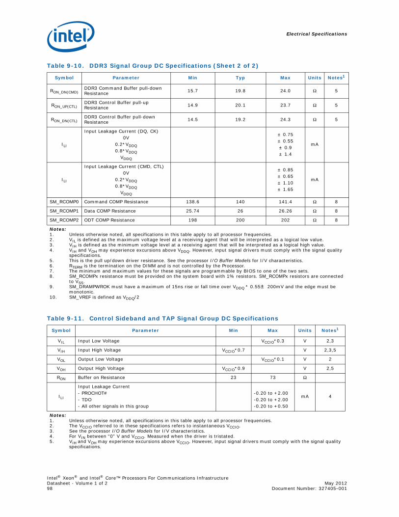
Electrical Specifications
Intel® Xeon® and Intel® Core™ Processors For Communications InfrastructureDatasheet - Volume 1 of 2 May 201298 Document Number: 327405-001
RON_DN(CMD)DDR3 Command Buffer pull-down Resistance 15.7 19.8 24.0 Ω 5
RON_UP(CTL)DDR3 Control Buffer pull-up Resistance 14.9 20.1 23.7 Ω 5
RON_DN(CTL)DDR3 Control Buffer pull-down Resistance 14.5 19.2 24.3 Ω 5
ILI
Input Leakage Current (DQ, CK)0V
0.2*VDDQ0.8*VDDQ
VDDQ
± 0.75± 0.55± 0.9± 1.4
mA
ILI
Input Leakage Current (CMD, CTL)0V
0.2*VDDQ0.8*VDDQ
VDDQ
± 0.85± 0.65± 1.10± 1.65
mA
SM_RCOMP0 Command COMP Resistance 138.6 140 141.4 Ω 8
SM_RCOMP1 Data COMP Resistance 25.74 26 26.26 Ω 8
SM_RCOMP2 ODT COMP Resistance 198 200 202 Ω 8
Notes:1. Unless otherwise noted, all specifications in this table apply to all processor frequencies.2. VIL is defined as the maximum voltage level at a receiving agent that will be interpreted as a logical low value.3. VIH is defined as the minimum voltage level at a receiving agent that will be interpreted as a logical high value.4. VIH and VOH may experience excursions above VDDQ. However, input signal drivers must comply with the signal quality
specifications.5. This is the pull up/down driver resistance. See the processor I/O Buffer Models for I/V characteristics.6. RTERM is the termination on the DIMM and is not controlled by the Processor.7. The minimum and maximum values for these signals are programmable by BIOS to one of the two sets. 8. SM_RCOMPx resistance must be provided on the system board with 1% resistors. SM_RCOMPx resistors are connected
to VSS.9. SM_DRAMPWROK must have a maximum of 15ns rise or fall time over VDDQ * 0.55± 200mV and the edge must be
monotonic.10. SM_VREF is defined as VDDQ/2
Table 9-11. Control Sideband and TAP Signal Group DC Specifications
Symbol Parameter Min Max Units Notes1
VIL Input Low Voltage VCCIO*0.3 V 2,3
VIH Input High Voltage VCCIO*0.7 V 2,3,5
VOL Output Low Voltage VCCIO*0.1 V 2
VOH Output High Voltage VCCIO*0.9 V 2,5
RON Buffer on Resistance 23 73 Ω
ILI
Input Leakage Current- PROCHOT#- TDO- All other signals in this group
-0.20 to +2.00-0.20 to +2.00-0.20 to +0.50
mA 4
Notes:1. Unless otherwise noted, all specifications in this table apply to all processor frequencies.2. The VCCIO referred to in these specifications refers to instantaneous VCCIO.3. See the processor I/O Buffer Models for I/V characteristics.4. For VIN between “0” V and VCCIO. Measured when the driver is tristated.5. VIH and VOH may experience excursions above VCCIO. However, input signal drivers must comply with the signal quality
specifications.
Table 9-10. DDR3 Signal Group DC Specifications (Sheet 2 of 2)
Symbol Parameter Min Typ Max Units Notes1
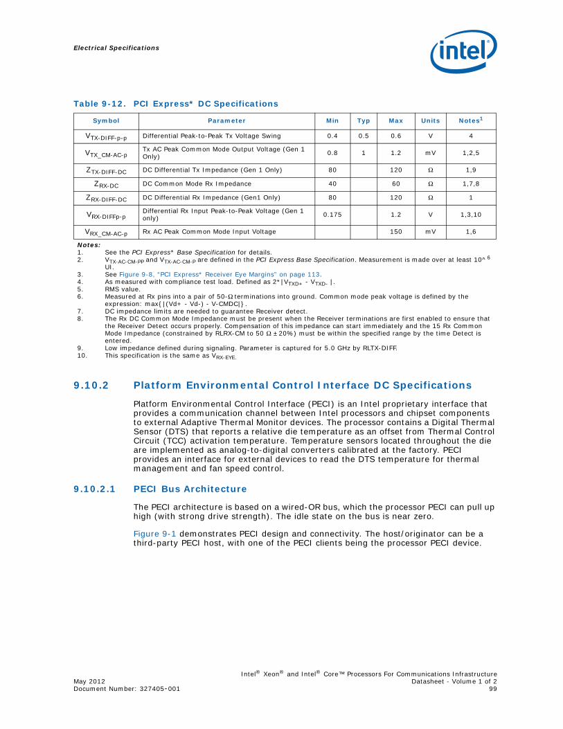
Electrical Specifications
Intel® Xeon® and Intel® Core™ Processors For Communications InfrastructureMay 2012 Datasheet - Volume 1 of 2Document Number: 327405-001 99
9.10.2 Platform Environmental Control Interface DC Specifications
Platform Environmental Control Interface (PECI) is an Intel proprietary interface that provides a communication channel between Intel processors and chipset components to external Adaptive Thermal Monitor devices. The processor contains a Digital Thermal Sensor (DTS) that reports a relative die temperature as an offset from Thermal Control Circuit (TCC) activation temperature. Temperature sensors located throughout the die are implemented as analog-to-digital converters calibrated at the factory. PECI provides an interface for external devices to read the DTS temperature for thermal management and fan speed control.
9.10.2.1 PECI Bus Architecture
The PECI architecture is based on a wired-OR bus, which the processor PECI can pull up high (with strong drive strength). The idle state on the bus is near zero.
Figure 9-1 demonstrates PECI design and connectivity. The host/originator can be a third-party PECI host, with one of the PECI clients being the processor PECI device.
Table 9-12. PCI Express* DC Specifications
Symbol Parameter Min Typ Max Units Notes1
VTX-DIFF-p-p Differential Peak-to-Peak Tx Voltage Swing 0.4 0.5 0.6 V 4
VTX_CM-AC-pTx AC Peak Common Mode Output Voltage (Gen 1 Only) 0.8 1 1.2 mV 1,2,5
ZTX-DIFF-DC DC Differential Tx Impedance (Gen 1 Only) 80 120 Ω 1,9
ZRX-DC DC Common Mode Rx Impedance 40 60 Ω 1,7,8
ZRX-DIFF-DC DC Differential Rx Impedance (Gen1 Only) 80 120 Ω 1
VRX-DIFFp-pDifferential Rx Input Peak-to-Peak Voltage (Gen 1 only) 0.175 1.2 V 1,3,10
VRX_CM-AC-p Rx AC Peak Common Mode Input Voltage 150 mV 1,6
Notes:1. See the PCI Express* Base Specification for details.2. VTX-AC-CM-PP and VTX-AC-CM-P are defined in the PCI Express Base Specification. Measurement is made over at least 10^6
UI.3. See Figure 9-8, “PCI Express* Receiver Eye Margins” on page 113.4. As measured with compliance test load. Defined as 2*|VTXD+ - VTXD- |. 5. RMS value.6. Measured at Rx pins into a pair of 50-Ω terminations into ground. Common mode peak voltage is defined by the
expression: max{|(Vd+ - Vd-) - V-CMDC|}.7. DC impedance limits are needed to guarantee Receiver detect. 8. The Rx DC Common Mode Impedance must be present when the Receiver terminations are first enabled to ensure that
the Receiver Detect occurs properly. Compensation of this impedance can start immediately and the 15 Rx Common Mode Impedance (constrained by RLRX-CM to 50 Ω ±20%) must be within the specified range by the time Detect is entered.
9. Low impedance defined during signaling. Parameter is captured for 5.0 GHz by RLTX-DIFF.10. This specification is the same as VRX-EYE.
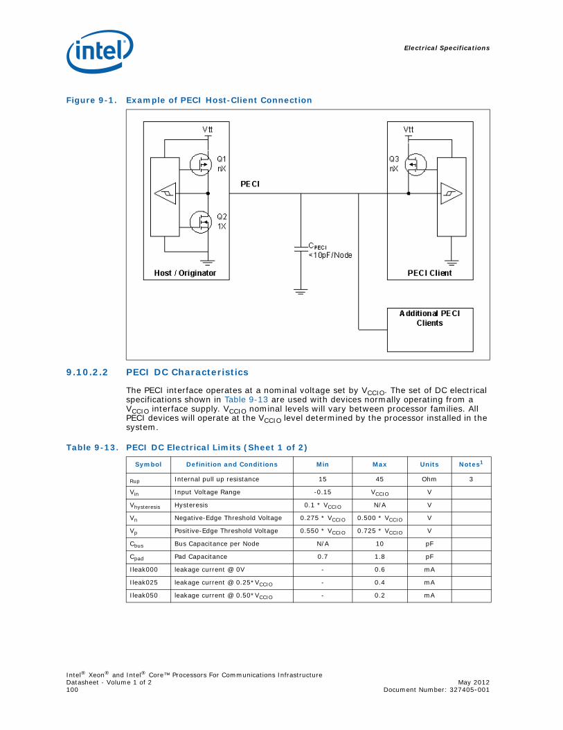
Electrical Specifications
Intel® Xeon® and Intel® Core™ Processors For Communications InfrastructureDatasheet - Volume 1 of 2 May 2012100 Document Number: 327405-001
9.10.2.2 PECI DC Characteristics
The PECI interface operates at a nominal voltage set by VCCIO. The set of DC electrical specifications shown in Table 9-13 are used with devices normally operating from a VCCIO interface supply. VCCIO nominal levels will vary between processor families. All PECI devices will operate at the VCCIO level determined by the processor installed in the system.
Figure 9-1. Example of PECI Host-Client Connection
Table 9-13. PECI DC Electrical Limits (Sheet 1 of 2)
Symbol Definition and Conditions Min Max Units Notes1
Rup Internal pull up resistance 15 45 Ohm 3
Vin Input Voltage Range -0.15 VCCIO V
Vhysteresis Hysteresis 0.1 * VCCIO N/A V
Vn Negative-Edge Threshold Voltage 0.275 * VCCIO 0.500 * VCCIO V
Vp Positive-Edge Threshold Voltage 0.550 * VCCIO 0.725 * VCCIO V
Cbus Bus Capacitance per Node N/A 10 pF
Cpad Pad Capacitance 0.7 1.8 pF
Ileak000 leakage current @ 0V - 0.6 mA
Ileak025 leakage current @ 0.25*VCCIO - 0.4 mA
Ileak050 leakage current @ 0.50*VCCIO - 0.2 mA
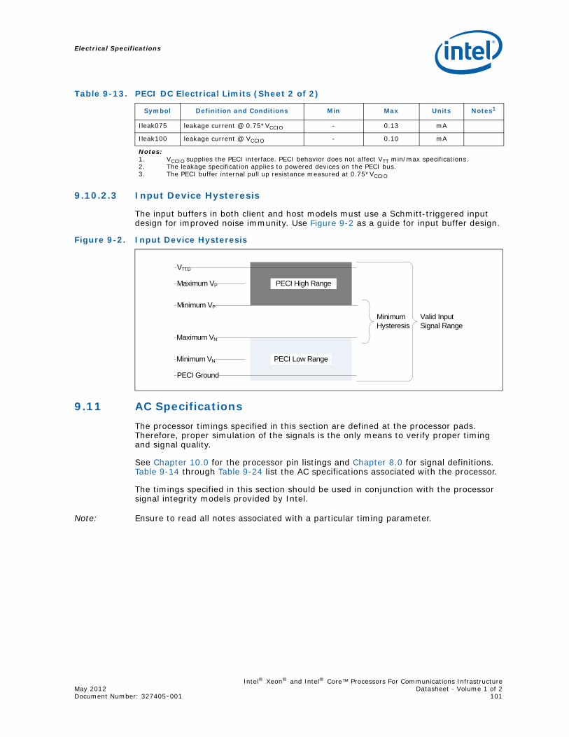
Electrical Specifications
Intel® Xeon® and Intel® Core™ Processors For Communications InfrastructureMay 2012 Datasheet - Volume 1 of 2Document Number: 327405-001 101
9.10.2.3 Input Device Hysteresis
The input buffers in both client and host models must use a Schmitt-triggered input design for improved noise immunity. Use Figure 9-2 as a guide for input buffer design.
9.11 AC SpecificationsThe processor timings specified in this section are defined at the processor pads. Therefore, proper simulation of the signals is the only means to verify proper timing and signal quality.
See Chapter 10.0 for the processor pin listings and Chapter 8.0 for signal definitions. Table 9-14 through Table 9-24 list the AC specifications associated with the processor.
The timings specified in this section should be used in conjunction with the processor signal integrity models provided by Intel.
Note: Ensure to read all notes associated with a particular timing parameter.
Ileak075 leakage current @ 0.75*VCCIO - 0.13 mA
Ileak100 leakage current @ VCCIO - 0.10 mA
Notes:1. VCCIO supplies the PECI interface. PECI behavior does not affect VTT min/max specifications.2. The leakage specification applies to powered devices on the PECI bus.3. The PECI buffer internal pull up resistance measured at 0.75*VCCIO
Table 9-13. PECI DC Electrical Limits (Sheet 2 of 2)
Symbol Definition and Conditions Min Max Units Notes1
Figure 9-2. Input Device Hysteresis
Minimum VP
Maximum VP
Minimum VN
Maximum VN
PECI High Range
PECI Low Range
Valid InputSignal Range
MinimumHysteresis
VTTD
PECI Ground

Electrical Specifications
Intel® Xeon® and Intel® Core™ Processors For Communications InfrastructureDatasheet - Volume 1 of 2 May 2012102 Document Number: 327405-001
Table 9-14. Differential Clocks (SSC on)
SSC ON 1CLK 1 μs 0.1 s 0.1 s 1 μs 1CLK
Signal Name
-Jitter c-c Abs
PerMin
-SSC ShortAvgMin
-ppm LongAvgMin
Ideal DC Target
+ppm Long
AvgMax
+SSC Short
AvgMax
+Jitter c-c Abs
PerMaxUnits
BCLK 9.849063 9.999063 10.02406 10.02506 10.02607 10.05120 10.20120 ns
Notes:1. Ideal DC Target: This serves only as an ideal reference target (0 ppm) to use for calculating the rest of the period
measurement values2. 0.1-second Measurement Window (frequency counter): Valuable measurement done using a frequency counter to
determine near DC average frequency (filtering out all jitter including SSC and cycle to cycle). This is used to determine if the system has a frequency static offset caused usually by incorrect crystal, crystal loading or incorrect clock configuration.
3. 1.0-μs Measurement Window (scope): This measurement is only used in conjunction with clock post processing software (Jit3 Advanced for example) with “filters = LPF 3RD order 1-MHz pole” to filter out high frequency jitter (FM) and show the underlying SSC profile. The numbers here bound the SSC min/ max excursions (SSC magnitude).
4. 1CLK - No Filter: Any 1 Period measured with a scope. Measured on a real time Oscilloscope using no filters, a simple period measurement (or a Jit3 period measurement - more accurate), provides absolute Min/Max timing information.
Table 9-15. Differential Clocks (SSC off)
SSC OFF 1CLK 0.1s 0.1s 1CLK
Signal Name -Jitter c-c AbsPerMin
-ppm LongAvgMin
Ideal DC target
+ppm LongAvgMax
+Jitter c-c AbsPerMax Units
BCLK 9.849000 9.999000 10.00000 10.00100 10.15100 ns
Notes:1. Ideal DC Target: This serves only as an ideal reference target (0ppm) to use for calculating the rest of the period
measurement values2. 0.1-second Measurement Window (frequency counter): Valuable measurement done using a frequency counter to
determine near DC average frequency (filtering out all jitter including SSC and cycle to cycle). This is used to determine if the system has a frequency static offset caused usually by incorrect crystal, crystal loading or incorrect clock configuration.
3. 1CLK - No Filter: Any 1 Period measured with a scope. Measured on a real time Oscilloscope using no filters, a simple period measurement (or a Jit3 period measurement - more accurate), provides absolute Min / Max timing information.
Table 9-16. Processor Clock Jitter Specifications (cycle-cycle)
Symbol Frequency(MHz) Type Source
(ps) Destination Notes
BCLKJIT_CC 100 Input Diff 150 processor/memory/PCI Express* 1
Notes:1. On all jitter measurements care should be taken to set the zero crossing voltage (for rising edge) of the clock to be the
point where the edge rate is the fastest. Using a Math function = Average (Derivative (Ch1)) and set the averages to 64, place the cursors where the slope is the highest on the rising edge - usually the lower half of the rising edge. This is defined because Flip Chip components prevent probing at the end of the transmission line. This will result in a reflection induced ledge in the middle of the rising edge and will significantly increase measured jitter.
Table 9-17. System Reference Clock DC and AC Specifications
Symbol Parameter Signal Min Max Unit Meas Figure Notes
Slew_rise Rising Slew Rate Diff 1.5 4.0 V/ns Avg 9-3 2,3
Slew_fall Falling Slew Rate Diff 1.5 4.0 V/ns Avg 9-3 2,3
Slew_var Slew Rate Matching Single Ended 20 % Avg 9-4 1,9
VSWING Differential Output Swing Diff 300 mV RT 9-3 2
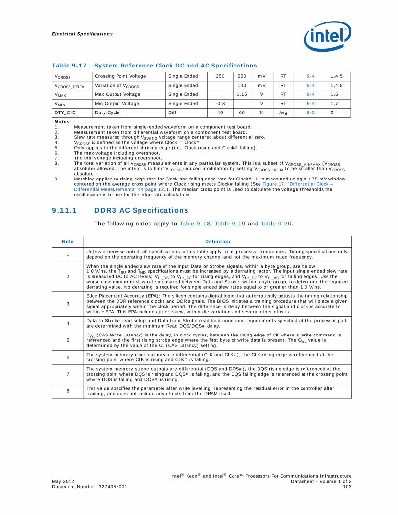
Electrical Specifications
Intel® Xeon® and Intel® Core™ Processors For Communications InfrastructureMay 2012 Datasheet - Volume 1 of 2Document Number: 327405-001 103
9.11.1 DDR3 AC Specifications
The following notes apply to Table 9-18, Table 9-19 and Table 9-20.
VCROSS Crossing Point Voltage Single Ended 250 550 mV RT 9-4 1,4,5
VCROSS_DELTA Variation of VCROSS Single Ended 140 mV RT 9-4 1,4,8
VMAX Max Output Voltage Single Ended 1.15 V RT 9-4 1,6
VMIN Min Output Voltage Single Ended -0.3 V RT 9-4 1,7
DTY_CYC Duty Cycle Diff 40 60 % Avg 9-3 2
Notes:1. Measurement taken from single-ended waveform on a component test board.2. Measurement taken from differential waveform on a component test board.3. Slew rate measured through VSWING voltage range centered about differential zero.4. VCROSS is defined as the voltage where Clock = Clock#.5. Only applies to the differential rising edge (i.e., Clock rising and Clock# falling).6. The max voltage including overshoot.7. The min voltage including undershoot.8. The total variation of all VCROSS measurements in any particular system. This is a subset of VCROSS_MIN/MAX (VCROSS
absolute) allowed. The intent is to limit VCROSS induced modulation by setting VCROSS_DELTA to be smaller than VCROSS absolute.
9. Matching applies to rising edge rate for Clock and falling edge rate for Clock#. It is measured using a ±75 mV window centered on the average cross point where Clock rising meets Clock# falling (See Figure 17, “Differential Clock – Differential Measurements” on page 121). The median cross point is used to calculate the voltage thresholds the oscilloscope is to use for the edge rate calculations.
Table 9-17. System Reference Clock DC and AC Specifications
Note Definition
1 Unless otherwise noted, all specifications in this table apply to all processor frequencies. Timing specifications only depend on the operating frequency of the memory channel and not the maximum rated frequency.
2
When the single ended slew rate of the input Data or Strobe signals, within a byte group, are below 1.0 V/ns, the TSU and THD specifications must be increased by a derrating factor. The input single ended slew rate is measured DC to AC levels; VIL_DC to VIH_AC for rising edges, and VIH_DC to VIL_AC for falling edges. Use the worse case minimum slew rate measured between Data and Strobe, within a byte group, to determine the required derrating value. No derrating is required for single ended slew rates equal to or greater than 1.0 V/ns.
3
Edge Placement Accuracy (EPA): The silicon contains digital logic that automatically adjusts the timing relationship between the DDR reference clocks and DDR signals. The BIOS initiates a training procedure that will place a given signal appropriately within the clock period. The difference in delay between the signal and clock is accurate to within ±EPA. This EPA includes jitter, skew, within die variation and several other effects.
4 Data to Strobe read setup and Data from Strobe read hold minimum requirements specified at the processor pad are determined with the minimum Read DQS/DQS# delay.
5CWL (CAS Write Latency) is the delay, in clock cycles, between the rising edge of CK where a write command is referenced and the first rising strobe edge where the first byte of write data is present. The CWL value is determined by the value of the CL (CAS Latency) setting.
6 The system memory clock outputs are differential (CLK and CLK#), the CLK rising edge is referenced at the crossing point where CLK is rising and CLK# is falling.
7The system memory strobe outputs are differential (DQS and DQS#), the DQS rising edge is referenced at the crossing point where DQS is rising and DQS# is falling, and the DQS falling edge is referenced at the crossing point where DQS is falling and DQS# is rising.
8 This value specifies the parameter after write levelling, representing the residual error in the controller after training, and does not include any effects from the DRAM itself.
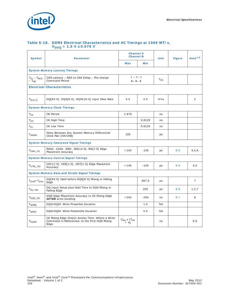
Electrical Specifications
Intel® Xeon® and Intel® Core™ Processors For Communications InfrastructureDatasheet - Volume 1 of 2 May 2012104 Document Number: 327405-001
Table 9-18. DDR3 Electrical Characteristics and AC Timings at 1066 MT/s,
VDDQ = 1.5 V ±0.075 V
Symbol Parameter
Channel AChannel B
Unit Figure Note1,9
Max Min
System Memory Latency Timings
TCL – TRCD – TRP
CAS Latency – RAS to CAS Delay – Pre-charge Command Period
7 – 7– 78– 8– 8
TCK
Electrical Characteristics
TSLR_D DQ[63:0], DQS[8:0], DQS#[8:0] Input Slew Rate 6.5 2.0 V/ns 2
System Memory Clock Timings
TCK CK Period 1.875 ns
TCH CK High Time 0.8125 ns
TCL CK Low Time 0.8125 ns
TSKEWSkew Between Any System Memory Differential Clock Pair (CK/CKB) 100 ps
System Memory Command Signal Timings
TCMD_CO RAS#, CAS#, WE#, MA[14:0], BA[2:0] Edge Placement Accuracy +145 -145 ps 9-5 3,4,6
System Memory Control Signal Timings
TCTRL_COCS#[1:0], CKE[1:0], ODT[1:0] Edge Placement Accuracy +145 -145 ps 9-5 3,6
System Memory Data and Strobe Signal Timings
TDVB+TDVADQ[63:0] Valid before DQS[8:0] Rising or Falling Edge 687.5 ps 7
TSu+HDDQ Input Setup plus Hold Time to DQS Rising or Falling Edge 200 ps 9-6 1,2,7
TDQS_CODQS Edge Placement Accuracy to CK Rising Edge AFTER write levelling +250 -250 ns 9-7 8
TWPRE DQS/DQS# Write Preamble Duration 1.0 Tck
TWPST DQS/DQS# Write Postamble Duration 0.5 Tck
TDQSS
CK Rising Edge Output Access Time, Where a Write Command Is Referenced, to the First DQS Rising Edge
CWL x (TCK + 4) ns 5,6
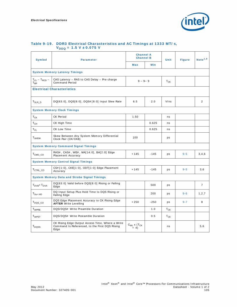
Electrical Specifications
Intel® Xeon® and Intel® Core™ Processors For Communications InfrastructureMay 2012 Datasheet - Volume 1 of 2Document Number: 327405-001 105
Table 9-19. DDR3 Electrical Characteristics and AC Timings at 1333 MT/s, VDDQ = 1.5 V ±0.075 V
Symbol Parameter
Channel AChannel B
Unit Figure Note1,9
Max Min
System Memory Latency Timings
TCL – TRCD – TRP
CAS Latency – RAS to CAS Delay – Pre-charge Command Period 9 – 9– 9 TCK
Electrical Characteristics
TSLR_D DQ[63:0], DQS[8:0], DQS#[8:0] Input Slew Rate 6.5 2.0 V/ns 2
System Memory Clock Timings
TCK CK Period 1.50 ns
TCH CK High Time 0.625 ns
TCL CK Low Time 0.625 ns
TSKEWSkew Between Any System Memory Differential Clock Pair (CK/CKB) 100 ps
System Memory Command Signal Timings
TCMD_CO RAS#, CAS#, WE#, MA[14:0], BA[2:0] Edge Placement Accuracy +145 -145 ps 9-5 3,4,6
System Memory Control Signal Timings
TCTRL_COCS#[1:0], CKE[1:0], ODT[1:0] Edge Placement Accuracy +145 -145 ps 9-5 3,6
System Memory Data and Strobe Signal Timings
TDVB+TDVADQ[63:0] Valid before DQS[8:0] Rising or Falling Edge 500 ps 7
TSu+HDDQ Input Setup Plus Hold Time to DQS Rising or Falling Edge 200 ps 9-6 1,2,7
TDQS_CODQS Edge Placement Accuracy to CK Rising Edge AFTER Write Levelling +250 -250 ps 9-7 8
TWPRE DQS/DQS# Write Preamble Duration 1.0 TCK
TWPST DQS/DQS# Write Postamble Duration 0.5 TCK
TDQSS
CK Rising Edge Output Access Time, Where a Write Command Is Referenced, to the First DQS Rising Edge
CWL x (TCK + 4) ns 5,6
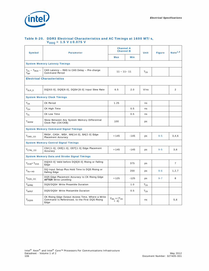
Electrical Specifications
Intel® Xeon® and Intel® Core™ Processors For Communications InfrastructureDatasheet - Volume 1 of 2 May 2012106 Document Number: 327405-001
Table 9-20. DDR3 Electrical Characteristics and AC Timings at 1600 MT/s, VDDQ = 1.5 V ±0.075 V
Symbol Parameter
Channel AChannel B
Unit Figure Note1,9
Max Min
System Memory Latency Timings
TCL – TRCD – TRP
CAS Latency – RAS to CAS Delay – Pre-charge Command Period 11 – 11– 11 TCK
Electrical Characteristics
TSLR_D DQ[63:0], DQS[8:0], DQS#[8:0] Input Slew Rate 6.5 2.0 V/ns 2
System Memory Clock Timings
TCK CK Period 1.25 ns
TCH CK High Time 0.5 ns
TCL CK Low Time 0.5 ns
TSKEWSkew Between Any System Memory Differential Clock Pair (CK/CKB) 100 ps
System Memory Command Signal Timings
TCMD_CO RAS#, CAS#, WE#, MA[14:0], BA[2:0] Edge Placement Accuracy +145 -145 ps 9-5 3,4,6
System Memory Control Signal Timings
TCTRL_COCS#[1:0], CKE[1:0], ODT[1:0] Edge Placement Accuracy +145 -145 ps 9-5 3,6
System Memory Data and Strobe Signal Timings
TDVB+TDVADQ[63:0] Valid before DQS[8:0] Rising or Falling Edge 375 ps 7
TSu+HDDQ Input Setup Plus Hold Time to DQS Rising or Falling Edge 200 ps 9-6 1,2,7
TDQS_CODQS Edge Placement Accuracy to CK Rising Edge AFTER Write Levelling +125 -125 ps 9-7 8
TWPRE DQS/DQS# Write Preamble Duration 1.0 TCK
TWPST DQS/DQS# Write Postamble Duration 0.5 TCK
TDQSS
CK Rising Edge Output Access Time, Where a Write Command Is Referenced, to the First DQS Rising Edge
CWL x (TCK + 4) ns 5,6
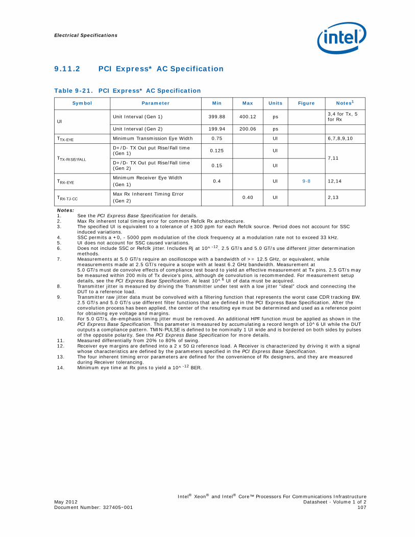
Electrical Specifications
Intel® Xeon® and Intel® Core™ Processors For Communications InfrastructureMay 2012 Datasheet - Volume 1 of 2Document Number: 327405-001 107
9.11.2 PCI Express* AC Specification
Table 9-21. PCI Express* AC Specification
Symbol Parameter Min Max Units Figure Notes1
UIUnit Interval (Gen 1) 399.88 400.12 ps 3,4 for Tx, 5
for Rx
Unit Interval (Gen 2) 199.94 200.06 ps
TTX-EYE Minimum Transmission Eye Width 0.75 UI 6,7,8,9,10
TTX-RISE/FALL
D+/D- TX Out put Rise/Fall time (Gen 1) 0.125 UI
7,11 D+/D- TX Out put Rise/Fall time (Gen 2) 0.15 UI
TRX-EYEMinimum Receiver Eye Width (Gen 1)
0.4 UI 9-8 12,14
TRX-TJ-CCMax Rx Inherent Timing Error (Gen 2)
0.40 UI 2,13
Notes:1. See the PCI Express Base Specification for details.2. Max Rx inherent total timing error for common Refclk Rx architecture. 3. The specified UI is equivalent to a tolerance of ±300 ppm for each Refclk source. Period does not account for SSC
induced variations.4. SSC permits a +0, - 5000 ppm modulation of the clock frequency at a modulation rate not to exceed 33 kHz.5. UI does not account for SSC caused variations.6. Does not include SSC or Refclk jitter. Includes Rj at 10^-12. 2.5 GT/s and 5.0 GT/s use different jitter determination
methods.7. Measurements at 5.0 GT/s require an oscilloscope with a bandwidth of >= 12.5 GHz, or equivalent, while
measurements made at 2.5 GT/s require a scope with at least 6.2 GHz bandwidth. Measurement at 5.0 GT/s must de convolve effects of compliance test board to yield an effective measurement at Tx pins. 2.5 GT/s may be measured within 200 mils of Tx device’s pins, although de convolution is recommended. For measurement setup details, see the PCI Express Base Specification. At least 10^6 UI of data must be acquired.
8. Transmitter jitter is measured by driving the Transmitter under test with a low jitter “ideal” clock and connecting the DUT to a reference load.
9. Transmitter raw jitter data must be convolved with a filtering function that represents the worst case CDR tracking BW. 2.5 GT/s and 5.0 GT/s use different filter functions that are defined in the PCI Express Base Specification. After the convolution process has been applied, the center of the resulting eye must be determined and used as a reference point for obtaining eye voltage and margins.
10. For 5.0 GT/s, de-emphasis timing jitter must be removed. An additional HPF function must be applied as shown in the PCI Express Base Specification. This parameter is measured by accumulating a record length of 10^6 UI while the DUT outputs a compliance pattern. TMIN-PULSE is defined to be nominally 1 UI wide and is bordered on both sides by pulses of the opposite polarity. See the PCI Express Base Specification for more details.
11. Measured differentially from 20% to 80% of swing.12. Receiver eye margins are defined into a 2 x 50 Ω reference load. A Receiver is characterized by driving it with a signal
whose characteristics are defined by the parameters specified in the PCI Express Base Specification.13. The four inherent timing error parameters are defined for the convenience of Rx designers, and they are measured
during Receiver tolerancing.14. Minimum eye time at Rx pins to yield a 10^-12 BER.
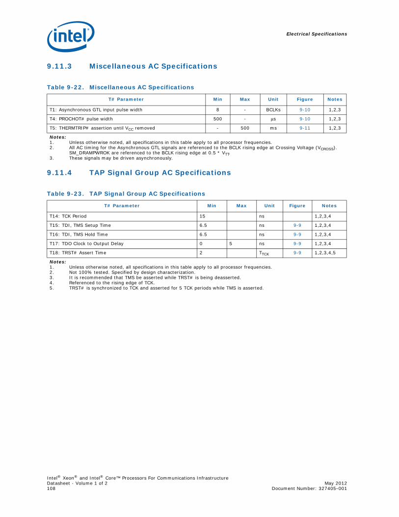
Electrical Specifications
Intel® Xeon® and Intel® Core™ Processors For Communications InfrastructureDatasheet - Volume 1 of 2 May 2012108 Document Number: 327405-001
9.11.3 Miscellaneous AC Specifications
9.11.4 TAP Signal Group AC Specifications
Table 9-22. Miscellaneous AC Specifications
T# Parameter Min Max Unit Figure Notes
T1: Asynchronous GTL input pulse width 8 - BCLKs 9-10 1,2,3
T4: PROCHOT# pulse width 500 - μs 9-10 1,2,3
T5: THERMTRIP# assertion until VCC removed - 500 ms 9-11 1,2,3
Notes:1. Unless otherwise noted, all specifications in this table apply to all processor frequencies.2. All AC timing for the Asynchronous GTL signals are referenced to the BCLK rising edge at Crossing Voltage (VCROSS).
SM_DRAMPWROK are referenced to the BCLK rising edge at 0.5 * VTT.3. These signals may be driven asynchronously.
Table 9-23. TAP Signal Group AC Specifications
T# Parameter Min Max Unit Figure Notes
T14: TCK Period 15 ns 1,2,3,4
T15: TDI, TMS Setup Time 6.5 ns 9-9 1,2,3,4
T16: TDI, TMS Hold Time 6.5 ns 9-9 1,2,3,4
T17: TDO Clock to Output Delay 0 5 ns 9-9 1,2,3,4
T18: TRST# Assert Time 2 TTCK 9-9 1,2,3,4,5
Notes:1. Unless otherwise noted, all specifications in this table apply to all processor frequencies.2. Not 100% tested. Specified by design characterization.3. It is recommended that TMS be asserted while TRST# is being deasserted.4. Referenced to the rising edge of TCK.5. TRST# is synchronized to TCK and asserted for 5 TCK periods while TMS is asserted.
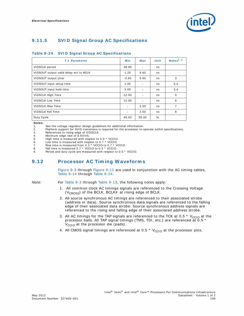
Electrical Specifications
Intel® Xeon® and Intel® Core™ Processors For Communications InfrastructureMay 2012 Datasheet - Volume 1 of 2Document Number: 327405-001 109
9.11.5 SVID Signal Group AC Specifications
9.12 Processor AC Timing WaveformsFigure 9-3 through Figure 9-11 are used in conjunction with the AC timing tables, Table 9-14 through Table 9-24.
Note: For Table 9-3 through Table 9-13, the following notes apply:1. All common clock AC timings signals are referenced to the Crossing Voltage
(VCROSS) of the BCLK, BCLK# at rising edge of BCLK.2. All source synchronous AC timings are referenced to their associated strobe
(address or data). Source synchronous data signals are referenced to the falling edge of their associated data strobe. Source synchronous address signals are referenced to the rising and falling edge of their associated address strobe.
3. All AC timings for the TAP signals are referenced to the TCK at 0.5 * VCCIO at the processor balls. All TAP signal timings (TMS, TDI, etc.) are referenced at 0.5 * VCCIO at the processor die (pads).
4. All CMOS signal timings are referenced at 0.5 * VCCIO at the processor pins.
Table 9-24. SVID Signal Group AC Specifications
T # Parameter Min Max Unit Notes1, 2
VIDSCLK period 38.90 - ns
VIDSOUT output valid delay wrt to BCLK 1.20 9.60 ns
VIDSOUT output jitter -3.60 0.65 ns 3
VIDSOUT input setup time 1.00 - ns 3,4
VIDSOUT input hold time 3.00 - ns 3,4
VIDSCLK High Time 12.00 - ns 5
VIDSCLK Low Time 12.00 - ns 6
VIDSCLK Rise Time - 2.50 ns 7
VIDSCLK Fall Time - 2.50 ns 8
Duty Cycle 45.00 55.00 %
Notes:1. See the voltage regulator design guidelines for additional information.2. Platform support for SVID transitions is required for the processor to operate within specifications.3. Referenced to rising edge of VIDSCLK.4. Minimum edge rate of 0.5V/nS.5. High time is measured with respect to 0.3 * VCCIO.6. Low time is measured with respect to 0.7 * VCCIO.7. Rise time is measured from 0.3 * VCCIO to 0.7 * VCCIO.8. Fall time is measured 0.7 * VCCIO to 0.3 * VCCIO.9. Period and duty cycle are measured with respect to 0.5 * VCCIO.
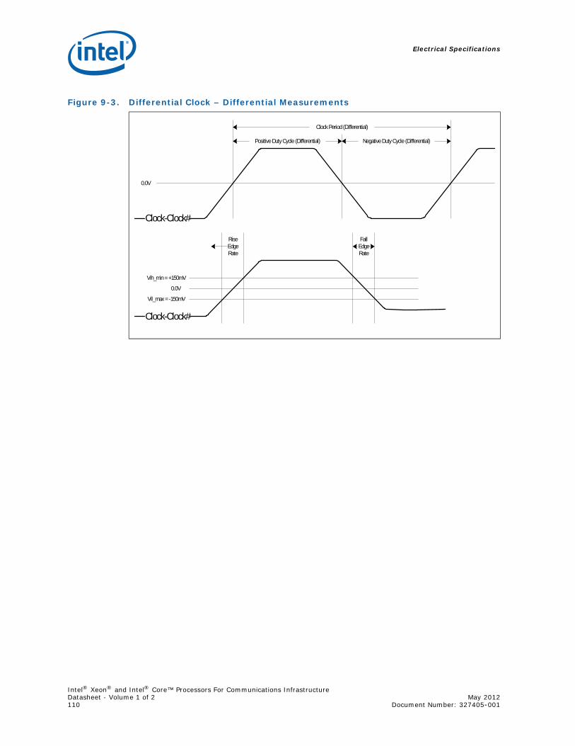
Electrical Specifications
Intel® Xeon® and Intel® Core™ Processors For Communications InfrastructureDatasheet - Volume 1 of 2 May 2012110 Document Number: 327405-001
Figure 9-3. Differential Clock – Differential Measurements
Clock-Clock#
Vih_min = +150mV
Vil_max = -150mV
Positive Duty Cycle (Differential)
0.0V
Clock-Clock#
0.0V
Negative Duty Cycle (Differential)
Clock Period (Differential)
Fall Edge Rate
Rise Edge Rate
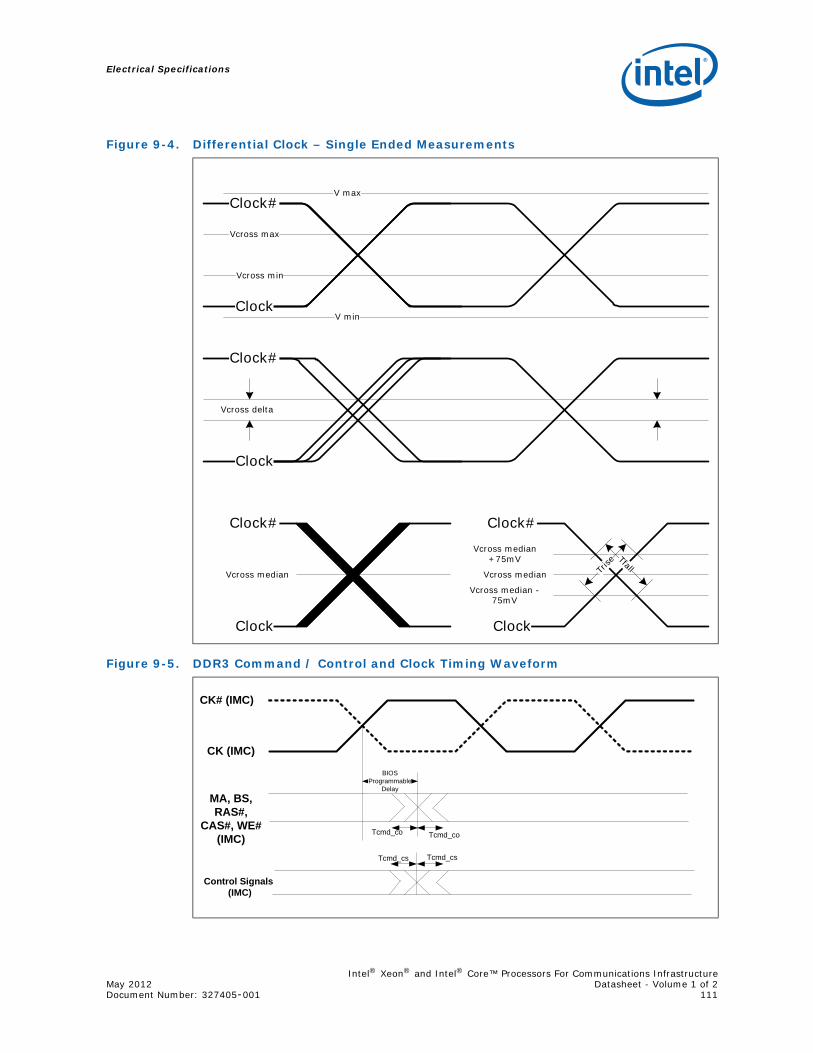
Electrical Specifications
Intel® Xeon® and Intel® Core™ Processors For Communications InfrastructureMay 2012 Datasheet - Volume 1 of 2Document Number: 327405-001 111
Figure 9-4. Differential Clock – Single Ended Measurements
Figure 9-5. DDR3 Command / Control and Clock Timing Waveform
V min
V max
Vcross max
Vcross min
Vcross delta
Clock#
Clock
Clock#
Vcross median
Clock
Clock#
Vcross median
Clock
Clock#Vcross median
+75mV
Vcross median -75mV
Trise
Tfall
Clock
CK# (IMC)
MA, BS, RAS#,
CAS#, WE# (IMC)
CK (IMC)
Control Signals (IMC)
Tcmd_co Tcmd_co
BIOS Programmable
Delay
Tcmd_csTcmd_cs
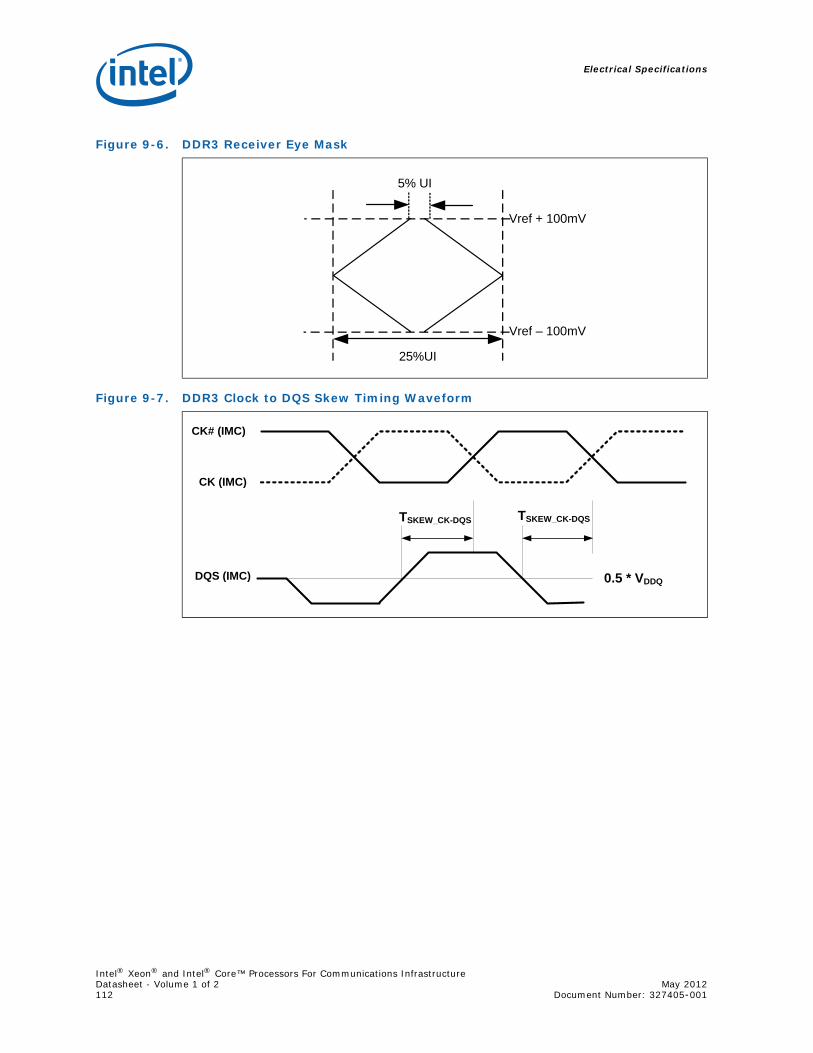
Electrical Specifications
Intel® Xeon® and Intel® Core™ Processors For Communications InfrastructureDatasheet - Volume 1 of 2 May 2012112 Document Number: 327405-001
Figure 9-6. DDR3 Receiver Eye Mask
Figure 9-7. DDR3 Clock to DQS Skew Timing Waveform
Vref + 100mV
Vref – 100mV
25%UI
5% UI
CK# (IMC)
DQS (IMC)
CK (IMC)
0.5 * VDDQ
TSKEW_CK-DQSTSKEW_CK-DQS
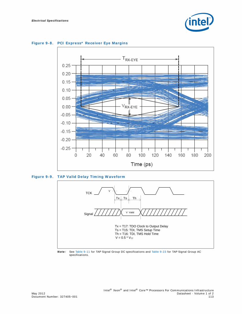
Electrical Specifications
Intel® Xeon® and Intel® Core™ Processors For Communications InfrastructureMay 2012 Datasheet - Volume 1 of 2Document Number: 327405-001 113
Note: See Table 9-11 for TAP Signal Group DC specifications and Table 9-23 for TAP Signal Group AC specifications.
Figure 9-8. PCI Express* Receiver Eye Margins
Figure 9-9. TAP Valid Delay Timing Waveform
Tx = T17: TDO Clock to Output DelayTs = T15: TDI, TMS Setup TimeTh = T16: TDI, TMS Hold TimeV = 0.5 * VTT
TCK
Signal
Tx Ts Th
V Valid
V
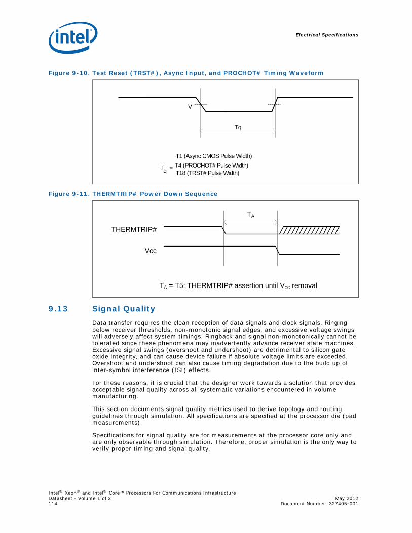
Electrical Specifications
Intel® Xeon® and Intel® Core™ Processors For Communications InfrastructureDatasheet - Volume 1 of 2 May 2012114 Document Number: 327405-001
9.13 Signal QualityData transfer requires the clean reception of data signals and clock signals. Ringing below receiver thresholds, non-monotonic signal edges, and excessive voltage swings will adversely affect system timings. Ringback and signal non-monotonically cannot be tolerated since these phenomena may inadvertently advance receiver state machines. Excessive signal swings (overshoot and undershoot) are detrimental to silicon gate oxide integrity, and can cause device failure if absolute voltage limits are exceeded. Overshoot and undershoot can also cause timing degradation due to the build up of inter-symbol interference (ISI) effects.
For these reasons, it is crucial that the designer work towards a solution that provides acceptable signal quality across all systematic variations encountered in volume manufacturing.
This section documents signal quality metrics used to derive topology and routing guidelines through simulation. All specifications are specified at the processor die (pad measurements).
Specifications for signal quality are for measurements at the processor core only and are only observable through simulation. Therefore, proper simulation is the only way to verify proper timing and signal quality.
Figure 9-10. Test Reset (TRST#), Async Input, and PROCHOT# Timing Waveform
Figure 9-11. THERMTRIP# Power Down Sequence
T18 (TRST# Pulse Width)
V
Tq =
Tq
T1 (Async CMOS Pulse Width)
T4 (PROCHOT# Pulse Width)
THERMTRIP#
Vcc
TA
TA = T5: THERMTRIP# assertion until VCC removal
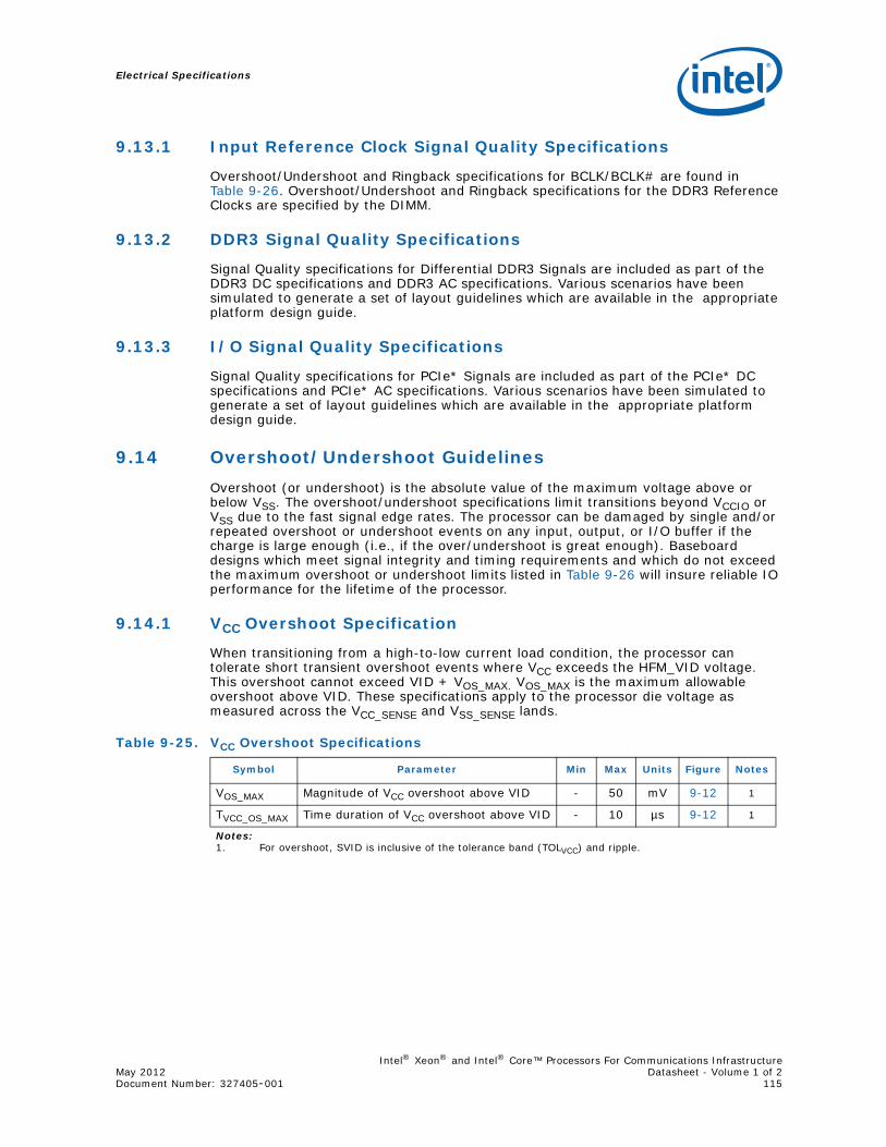
Electrical Specifications
Intel® Xeon® and Intel® Core™ Processors For Communications InfrastructureMay 2012 Datasheet - Volume 1 of 2Document Number: 327405-001 115
9.13.1 Input Reference Clock Signal Quality Specifications
Overshoot/Undershoot and Ringback specifications for BCLK/BCLK# are found in Table 9-26. Overshoot/Undershoot and Ringback specifications for the DDR3 Reference Clocks are specified by the DIMM.
9.13.2 DDR3 Signal Quality Specifications
Signal Quality specifications for Differential DDR3 Signals are included as part of the DDR3 DC specifications and DDR3 AC specifications. Various scenarios have been simulated to generate a set of layout guidelines which are available in the appropriate platform design guide.
9.13.3 I/O Signal Quality Specifications
Signal Quality specifications for PCIe* Signals are included as part of the PCIe* DC specifications and PCIe* AC specifications. Various scenarios have been simulated to generate a set of layout guidelines which are available in the appropriate platform design guide.
9.14 Overshoot/Undershoot GuidelinesOvershoot (or undershoot) is the absolute value of the maximum voltage above or below VSS. The overshoot/undershoot specifications limit transitions beyond VCCIO or VSS due to the fast signal edge rates. The processor can be damaged by single and/or repeated overshoot or undershoot events on any input, output, or I/O buffer if the charge is large enough (i.e., if the over/undershoot is great enough). Baseboard designs which meet signal integrity and timing requirements and which do not exceed the maximum overshoot or undershoot limits listed in Table 9-26 will insure reliable IO performance for the lifetime of the processor.
9.14.1 VCC Overshoot Specification
When transitioning from a high-to-low current load condition, the processor can tolerate short transient overshoot events where VCC exceeds the HFM_VID voltage. This overshoot cannot exceed VID + VOS_MAX. VOS_MAX is the maximum allowable overshoot above VID. These specifications apply to the processor die voltage as measured across the VCC_SENSE and VSS_SENSE lands.
Table 9-25. VCC Overshoot Specifications
Symbol Parameter Min Max Units Figure Notes
VOS_MAX Magnitude of VCC overshoot above VID - 50 mV 9-12 1
TVCC_OS_MAX Time duration of VCC overshoot above VID - 10 µs 9-12 1
Notes:1. For overshoot, SVID is inclusive of the tolerance band (TOLVCC) and ripple.
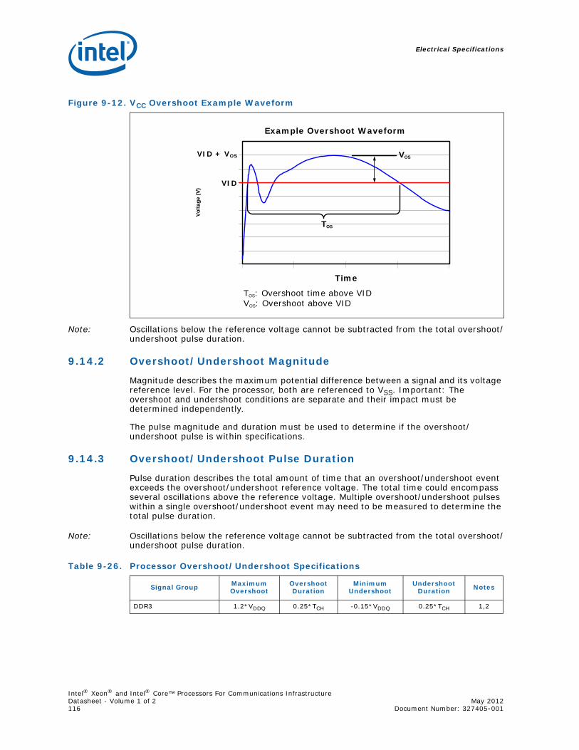
Electrical Specifications
Intel® Xeon® and Intel® Core™ Processors For Communications InfrastructureDatasheet - Volume 1 of 2 May 2012116 Document Number: 327405-001
Note: Oscillations below the reference voltage cannot be subtracted from the total overshoot/undershoot pulse duration.
9.14.2 Overshoot/Undershoot Magnitude
Magnitude describes the maximum potential difference between a signal and its voltage reference level. For the processor, both are referenced to VSS. Important: The overshoot and undershoot conditions are separate and their impact must be determined independently.
The pulse magnitude and duration must be used to determine if the overshoot/undershoot pulse is within specifications.
9.14.3 Overshoot/Undershoot Pulse Duration
Pulse duration describes the total amount of time that an overshoot/undershoot event exceeds the overshoot/undershoot reference voltage. The total time could encompass several oscillations above the reference voltage. Multiple overshoot/undershoot pulses within a single overshoot/undershoot event may need to be measured to determine the total pulse duration.
Note: Oscillations below the reference voltage cannot be subtracted from the total overshoot/undershoot pulse duration.
Figure 9-12. VCC Overshoot Example Waveform
Time
Example Overshoot Waveform
Vo
ltag
e (
V)
VID
VID + VOS
TOS
VOS
TOS: Overshoot time above VIDVOS: Overshoot above VID
Table 9-26. Processor Overshoot/Undershoot Specifications
Signal Group Maximum Overshoot
Overshoot Duration
Minimum Undershoot
Undershoot Duration Notes
DDR3 1.2*VDDQ 0.25*TCH -0.15*VDDQ 0.25*TCH 1,2
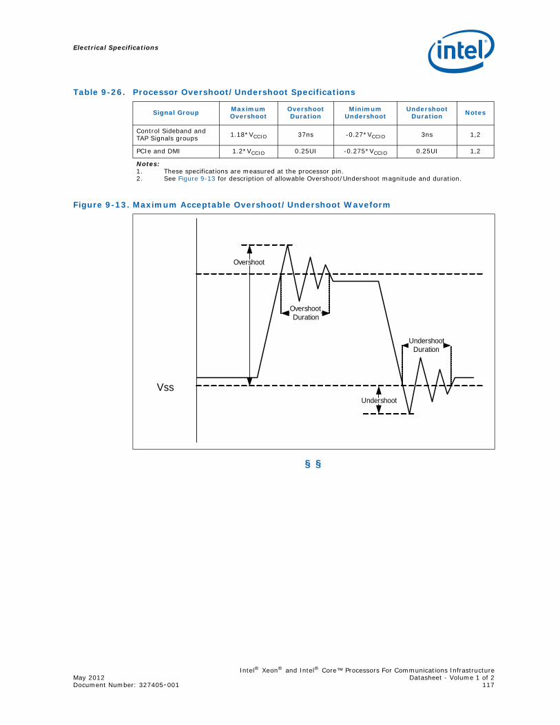
Electrical Specifications
Intel® Xeon® and Intel® Core™ Processors For Communications InfrastructureMay 2012 Datasheet - Volume 1 of 2Document Number: 327405-001 117
§ §
Control Sideband and TAP Signals groups 1.18*VCCIO 37ns -0.27*VCCIO 3ns 1,2
PCIe and DMI 1.2*VCCIO 0.25UI -0.275*VCCIO 0.25UI 1,2
Notes:1. These specifications are measured at the processor pin.2. See Figure 9-13 for description of allowable Overshoot/Undershoot magnitude and duration.
Figure 9-13. Maximum Acceptable Overshoot/Undershoot Waveform
Table 9-26. Processor Overshoot/Undershoot Specifications
Signal Group Maximum Overshoot
Overshoot Duration
Minimum Undershoot
Undershoot Duration Notes
Vss
Overshoot Duration
Undershoot Duration
Overshoot
Undershoot

Electrical Specifications
Intel® Xeon® and Intel® Core™ Processors For Communications InfrastructureDatasheet - Volume 1 of 2 May 2012118 Document Number: 327405-001

Processor Ball and Package Information
Intel® Xeon® and Intel® Core™ Processors For Communications InfrastructureMay 2012 Datasheet - Volume 1 of 2Document Number: 327405-001 119
10.0 Processor Ball and Package Information
10.1 Processor Ball Assignments• Table 10-1 provides a listing of all processor pins ordered alphabetically by ball
name.• Table 10-2 provides a listing of all processor pins ordered alphabetically by ball
number.• Figure 10-1, Figure 10-2, Figure 10-3, and Figure 10-4 show the bottom view of
the processor ballmap.
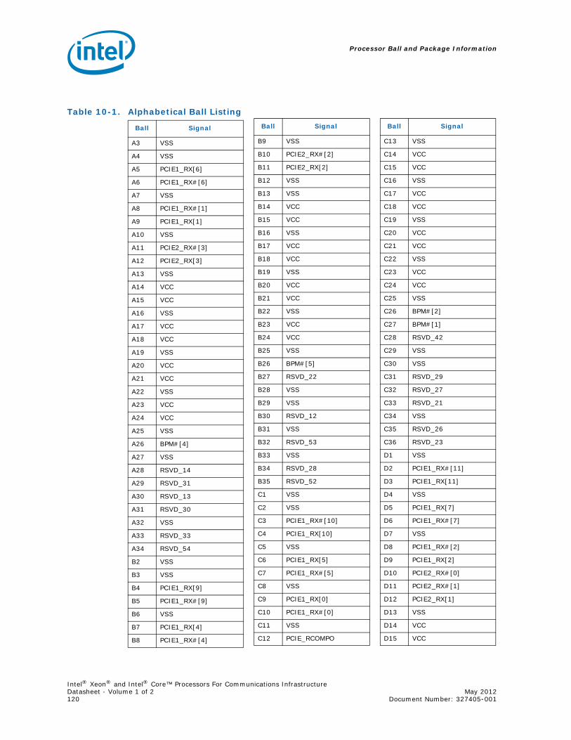
Intel® Xeon® and Intel® Core™ Processors For Communications InfrastructureDatasheet - Volume 1 of 2 May 2012120 Document Number: 327405-001
Processor Ball and Package Information
Table 10-1. Alphabetical Ball Listing
Ball Signal
A3 VSS
A4 VSS
A5 PCIE1_RX[6]
A6 PCIE1_RX#[6]
A7 VSS
A8 PCIE1_RX#[1]
A9 PCIE1_RX[1]
A10 VSS
A11 PCIE2_RX#[3]
A12 PCIE2_RX[3]
A13 VSS
A14 VCC
A15 VCC
A16 VSS
A17 VCC
A18 VCC
A19 VSS
A20 VCC
A21 VCC
A22 VSS
A23 VCC
A24 VCC
A25 VSS
A26 BPM#[4]
A27 VSS
A28 RSVD_14
A29 RSVD_31
A30 RSVD_13
A31 RSVD_30
A32 VSS
A33 RSVD_33
A34 RSVD_54
B2 VSS
B3 VSS
B4 PCIE1_RX[9]
B5 PCIE1_RX#[9]
B6 VSS
B7 PCIE1_RX[4]
B8 PCIE1_RX#[4]
B9 VSS
B10 PCIE2_RX#[2]
B11 PCIE2_RX[2]
B12 VSS
B13 VSS
B14 VCC
B15 VCC
B16 VSS
B17 VCC
B18 VCC
B19 VSS
B20 VCC
B21 VCC
B22 VSS
B23 VCC
B24 VCC
B25 VSS
B26 BPM#[5]
B27 RSVD_22
B28 VSS
B29 VSS
B30 RSVD_12
B31 VSS
B32 RSVD_53
B33 VSS
B34 RSVD_28
B35 RSVD_52
C1 VSS
C2 VSS
C3 PCIE1_RX#[10]
C4 PCIE1_RX[10]
C5 VSS
C6 PCIE1_RX[5]
C7 PCIE1_RX#[5]
C8 VSS
C9 PCIE1_RX[0]
C10 PCIE1_RX#[0]
C11 VSS
C12 PCIE_RCOMPO
Ball Signal
C13 VSS
C14 VCC
C15 VCC
C16 VSS
C17 VCC
C18 VCC
C19 VSS
C20 VCC
C21 VCC
C22 VSS
C23 VCC
C24 VCC
C25 VSS
C26 BPM#[2]
C27 BPM#[1]
C28 RSVD_42
C29 VSS
C30 VSS
C31 RSVD_29
C32 RSVD_27
C33 RSVD_21
C34 VSS
C35 RSVD_26
C36 RSVD_23
D1 VSS
D2 PCIE1_RX#[11]
D3 PCIE1_RX[11]
D4 VSS
D5 PCIE1_RX[7]
D6 PCIE1_RX#[7]
D7 VSS
D8 PCIE1_RX#[2]
D9 PCIE1_RX[2]
D10 PCIE2_RX#[0]
D11 PCIE2_RX#[1]
D12 PCIE2_RX[1]
D13 VSS
D14 VCC
D15 VCC
Ball Signal
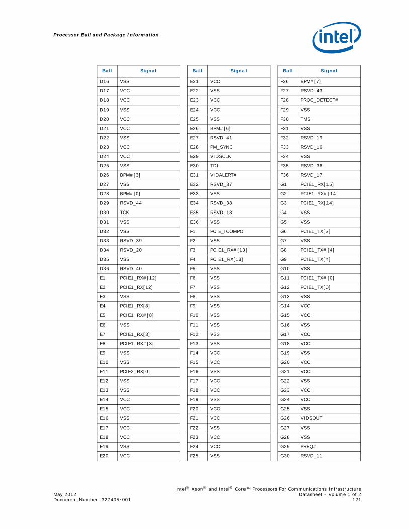
Intel® Xeon® and Intel® Core™ Processors For Communications InfrastructureMay 2012 Datasheet - Volume 1 of 2Document Number: 327405-001 121
Processor Ball and Package Information
D16 VSS
D17 VCC
D18 VCC
D19 VSS
D20 VCC
D21 VCC
D22 VSS
D23 VCC
D24 VCC
D25 VSS
D26 BPM#[3]
D27 VSS
D28 BPM#[0]
D29 RSVD_44
D30 TCK
D31 VSS
D32 VSS
D33 RSVD_39
D34 RSVD_20
D35 VSS
D36 RSVD_40
E1 PCIE1_RX#[12]
E2 PCIE1_RX[12]
E3 VSS
E4 PCIE1_RX[8]
E5 PCIE1_RX#[8]
E6 VSS
E7 PCIE1_RX[3]
E8 PCIE1_RX#[3]
E9 VSS
E10 VSS
E11 PCIE2_RX[0]
E12 VSS
E13 VSS
E14 VCC
E15 VCC
E16 VSS
E17 VCC
E18 VCC
E19 VSS
E20 VCC
Ball Signal
E21 VCC
E22 VSS
E23 VCC
E24 VCC
E25 VSS
E26 BPM#[6]
E27 RSVD_41
E28 PM_SYNC
E29 VIDSCLK
E30 TDI
E31 VIDALERT#
E32 RSVD_37
E33 VSS
E34 RSVD_38
E35 RSVD_18
E36 VSS
F1 PCIE_ICOMPO
F2 VSS
F3 PCIE1_RX#[13]
F4 PCIE1_RX[13]
F5 VSS
F6 VSS
F7 VSS
F8 VSS
F9 VSS
F10 VSS
F11 VSS
F12 VSS
F13 VSS
F14 VCC
F15 VCC
F16 VSS
F17 VCC
F18 VCC
F19 VSS
F20 VCC
F21 VCC
F22 VSS
F23 VCC
F24 VCC
F25 VSS
Ball Signal
F26 BPM#[7]
F27 RSVD_43
F28 PROC_DETECT#
F29 VSS
F30 TMS
F31 VSS
F32 RSVD_19
F33 RSVD_16
F34 VSS
F35 RSVD_36
F36 RSVD_17
G1 PCIE1_RX[15]
G2 PCIE1_RX#[14]
G3 PCIE1_RX[14]
G4 VSS
G5 VSS
G6 PCIE1_TX[7]
G7 VSS
G8 PCIE1_TX#[4]
G9 PCIE1_TX[4]
G10 VSS
G11 PCIE1_TX#[0]
G12 PCIE1_TX[0]
G13 VSS
G14 VCC
G15 VCC
G16 VSS
G17 VCC
G18 VCC
G19 VSS
G20 VCC
G21 VCC
G22 VSS
G23 VCC
G24 VCC
G25 VSS
G26 VIDSOUT
G27 VSS
G28 VSS
G29 PREQ#
G30 RSVD_11
Ball Signal
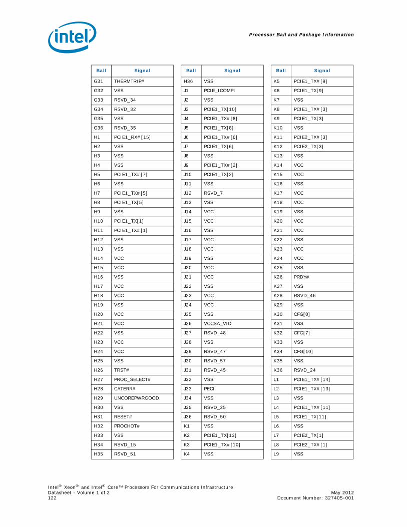
Intel® Xeon® and Intel® Core™ Processors For Communications InfrastructureDatasheet - Volume 1 of 2 May 2012122 Document Number: 327405-001
Processor Ball and Package Information
G31 THERMTRIP#
G32 VSS
G33 RSVD_34
G34 RSVD_32
G35 VSS
G36 RSVD_35
H1 PCIE1_RX#[15]
H2 VSS
H3 VSS
H4 VSS
H5 PCIE1_TX#[7]
H6 VSS
H7 PCIE1_TX#[5]
H8 PCIE1_TX[5]
H9 VSS
H10 PCIE1_TX[1]
H11 PCIE1_TX#[1]
H12 VSS
H13 VSS
H14 VCC
H15 VCC
H16 VSS
H17 VCC
H18 VCC
H19 VSS
H20 VCC
H21 VCC
H22 VSS
H23 VCC
H24 VCC
H25 VSS
H26 TRST#
H27 PROC_SELECT#
H28 CATERR#
H29 UNCOREPWRGOOD
H30 VSS
H31 RESET#
H32 PROCHOT#
H33 VSS
H34 RSVD_15
H35 RSVD_51
Ball Signal
H36 VSS
J1 PCIE_ICOMPI
J2 VSS
J3 PCIE1_TX[10]
J4 PCIE1_TX#[8]
J5 PCIE1_TX[8]
J6 PCIE1_TX#[6]
J7 PCIE1_TX[6]
J8 VSS
J9 PCIE1_TX#[2]
J10 PCIE1_TX[2]
J11 VSS
J12 RSVD_7
J13 VSS
J14 VCC
J15 VCC
J16 VSS
J17 VCC
J18 VCC
J19 VSS
J20 VCC
J21 VCC
J22 VSS
J23 VCC
J24 VCC
J25 VSS
J26 VCCSA_VID
J27 RSVD_48
J28 VSS
J29 RSVD_47
J30 RSVD_57
J31 RSVD_45
J32 VSS
J33 PECI
J34 VSS
J35 RSVD_25
J36 RSVD_50
K1 VSS
K2 PCIE1_TX[13]
K3 PCIE1_TX#[10]
K4 VSS
Ball Signal
K5 PCIE1_TX#[9]
K6 PCIE1_TX[9]
K7 VSS
K8 PCIE1_TX#[3]
K9 PCIE1_TX[3]
K10 VSS
K11 PCIE2_TX#[3]
K12 PCIE2_TX[3]
K13 VSS
K14 VCC
K15 VCC
K16 VSS
K17 VCC
K18 VCC
K19 VSS
K20 VCC
K21 VCC
K22 VSS
K23 VCC
K24 VCC
K25 VSS
K26 PRDY#
K27 VSS
K28 RSVD_46
K29 VSS
K30 CFG[0]
K31 VSS
K32 CFG[7]
K33 VSS
K34 CFG[10]
K35 VSS
K36 RSVD_24
L1 PCIE1_TX#[14]
L2 PCIE1_TX#[13]
L3 VSS
L4 PCIE1_TX#[11]
L5 PCIE1_TX[11]
L6 VSS
L7 PCIE2_TX[1]
L8 PCIE2_TX#[1]
L9 VSS
Ball Signal
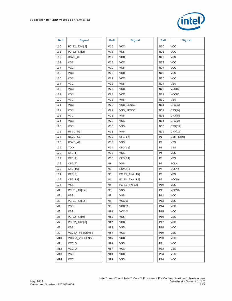
Intel® Xeon® and Intel® Core™ Processors For Communications InfrastructureMay 2012 Datasheet - Volume 1 of 2Document Number: 327405-001 123
Processor Ball and Package Information
L10 PCIE2_TX#[2]
L11 PCIE2_TX[2]
L12 RSVD_8
L13 VSS
L14 VCC
L15 VCC
L16 VSS
L17 VCC
L18 VCC
L19 VSS
L20 VCC
L21 VCC
L22 VSS
L23 VCC
L24 VCC
L25 VSS
L26 RSVD_55
L27 RSVD_56
L28 RSVD_49
L29 TDO
L30 CFG[1]
L31 CFG[4]
L32 CFG[5]
L33 CFG[16]
L34 CFG[9]
L35 CFG[13]
L36 VSS
M1 PCIE1_TX[14]
M2 VSS
M3 PCIE1_TX[15]
M4 VSS
M5 VSS
M6 PCIE2_TX[0]
M7 PCIE2_TX#[0]
M8 VSS
M9 VCCSA_VSSSENSE
M10 VCCSA_VCCSENSE
M11 VCCIO
M12 VCCIO
M13 VSS
M14 VCC
Ball Signal
M15 VCC
M16 VSS
M17 VCC
M18 VCC
M19 VSS
M20 VCC
M21 VCC
M22 VSS
M23 VCC
M24 VCC
M25 VSS
M26 VCC_SENSE
M27 VSS_SENSE
M28 VSS
M29 VSS
M30 VSS
M31 VSS
M32 CFG[17]
M33 VSS
M34 CFG[11]
M35 VSS
M36 CFG[14]
N1 VSS
N2 RSVD_6
N3 PCIE1_TX#[15]
N4 PCIE1_TX#[12]
N5 PCIE1_TX[12]
N6 VSS
N7 VSS
N8 VCCIO
N9 VCCSA
N10 VCCIO
N11 VSS
N12 VCC
N13 VSS
N14 VCC
N15 VCC
N16 VSS
N17 VCC
N18 VCC
N19 VSS
Ball Signal
N20 VCC
N21 VCC
N22 VSS
N23 VCC
N24 VCC
N25 VSS
N26 VCC
N27 VSS
N28 VCCIO
N29 VCCIO
N30 VSS
N31 CFG[3]
N32 CFG[6]
N33 CFG[8]
N34 CFG[2]
N35 CFG[12]
N36 CFG[15]
P1 DMI_TX[0]
P2 VSS
P3 VSS
P4 VSS
P5 VSS
P6 BCLK
P7 BCLK#
P8 VSS
P9 VCCSA
P10 VSS
P11 VCCSA
P12 VCC
P13 VSS
P14 VCC
P15 VCC
P16 VSS
P17 VCC
P18 VCC
P19 VSS
P20 VCC
P21 VCC
P22 VSS
P23 VCC
P24 VCC
Ball Signal
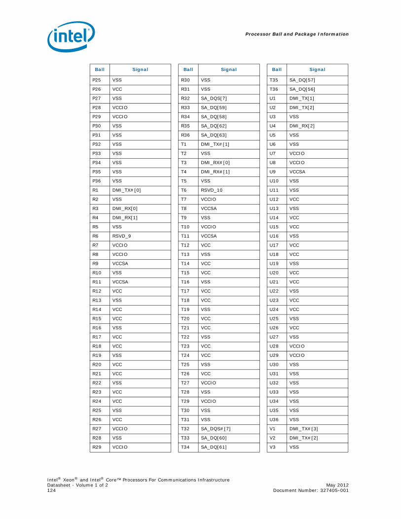
Intel® Xeon® and Intel® Core™ Processors For Communications InfrastructureDatasheet - Volume 1 of 2 May 2012124 Document Number: 327405-001
Processor Ball and Package Information
P25 VSS
P26 VCC
P27 VSS
P28 VCCIO
P29 VCCIO
P30 VSS
P31 VSS
P32 VSS
P33 VSS
P34 VSS
P35 VSS
P36 VSS
R1 DMI_TX#[0]
R2 VSS
R3 DMI_RX[0]
R4 DMI_RX[1]
R5 VSS
R6 RSVD_9
R7 VCCIO
R8 VCCIO
R9 VCCSA
R10 VSS
R11 VCCSA
R12 VCC
R13 VSS
R14 VCC
R15 VCC
R16 VSS
R17 VCC
R18 VCC
R19 VSS
R20 VCC
R21 VCC
R22 VSS
R23 VCC
R24 VCC
R25 VSS
R26 VCC
R27 VCCIO
R28 VSS
R29 VCCIO
Ball Signal
R30 VSS
R31 VSS
R32 SA_DQS[7]
R33 SA_DQ[59]
R34 SA_DQ[58]
R35 SA_DQ[62]
R36 SA_DQ[63]
T1 DMI_TX#[1]
T2 VSS
T3 DMI_RX#[0]
T4 DMI_RX#[1]
T5 VSS
T6 RSVD_10
T7 VCCIO
T8 VCCSA
T9 VSS
T10 VCCIO
T11 VCCSA
T12 VCC
T13 VSS
T14 VCC
T15 VCC
T16 VSS
T17 VCC
T18 VCC
T19 VSS
T20 VCC
T21 VCC
T22 VSS
T23 VCC
T24 VCC
T25 VSS
T26 VCC
T27 VCCIO
T28 VSS
T29 VCCIO
T30 VSS
T31 VSS
T32 SA_DQS#[7]
T33 SA_DQ[60]
T34 SA_DQ[61]
Ball Signal
T35 SA_DQ[57]
T36 SA_DQ[56]
U1 DMI_TX[1]
U2 DMI_TX[2]
U3 VSS
U4 DMI_RX[2]
U5 VSS
U6 VSS
U7 VCCIO
U8 VCCIO
U9 VCCSA
U10 VSS
U11 VSS
U12 VCC
U13 VSS
U14 VCC
U15 VCC
U16 VSS
U17 VCC
U18 VCC
U19 VSS
U20 VCC
U21 VCC
U22 VSS
U23 VCC
U24 VCC
U25 VSS
U26 VCC
U27 VSS
U28 VCCIO
U29 VCCIO
U30 VSS
U31 VSS
U32 VSS
U33 VSS
U34 VSS
U35 VSS
U36 VSS
V1 DMI_TX#[3]
V2 DMI_TX#[2]
V3 VSS
Ball Signal
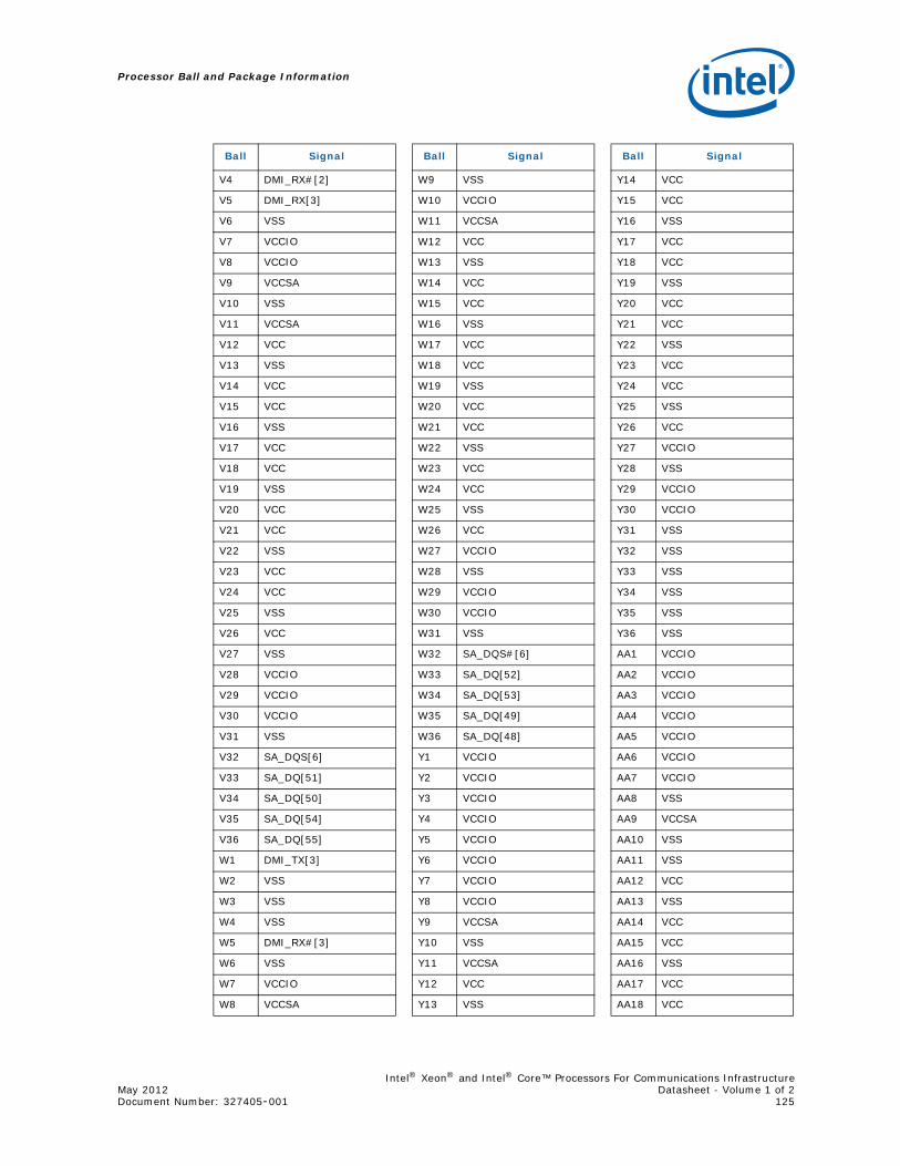
Intel® Xeon® and Intel® Core™ Processors For Communications InfrastructureMay 2012 Datasheet - Volume 1 of 2Document Number: 327405-001 125
Processor Ball and Package Information
V4 DMI_RX#[2]
V5 DMI_RX[3]
V6 VSS
V7 VCCIO
V8 VCCIO
V9 VCCSA
V10 VSS
V11 VCCSA
V12 VCC
V13 VSS
V14 VCC
V15 VCC
V16 VSS
V17 VCC
V18 VCC
V19 VSS
V20 VCC
V21 VCC
V22 VSS
V23 VCC
V24 VCC
V25 VSS
V26 VCC
V27 VSS
V28 VCCIO
V29 VCCIO
V30 VCCIO
V31 VSS
V32 SA_DQS[6]
V33 SA_DQ[51]
V34 SA_DQ[50]
V35 SA_DQ[54]
V36 SA_DQ[55]
W1 DMI_TX[3]
W2 VSS
W3 VSS
W4 VSS
W5 DMI_RX#[3]
W6 VSS
W7 VCCIO
W8 VCCSA
Ball Signal
W9 VSS
W10 VCCIO
W11 VCCSA
W12 VCC
W13 VSS
W14 VCC
W15 VCC
W16 VSS
W17 VCC
W18 VCC
W19 VSS
W20 VCC
W21 VCC
W22 VSS
W23 VCC
W24 VCC
W25 VSS
W26 VCC
W27 VCCIO
W28 VSS
W29 VCCIO
W30 VCCIO
W31 VSS
W32 SA_DQS#[6]
W33 SA_DQ[52]
W34 SA_DQ[53]
W35 SA_DQ[49]
W36 SA_DQ[48]
Y1 VCCIO
Y2 VCCIO
Y3 VCCIO
Y4 VCCIO
Y5 VCCIO
Y6 VCCIO
Y7 VCCIO
Y8 VCCIO
Y9 VCCSA
Y10 VSS
Y11 VCCSA
Y12 VCC
Y13 VSS
Ball Signal
Y14 VCC
Y15 VCC
Y16 VSS
Y17 VCC
Y18 VCC
Y19 VSS
Y20 VCC
Y21 VCC
Y22 VSS
Y23 VCC
Y24 VCC
Y25 VSS
Y26 VCC
Y27 VCCIO
Y28 VSS
Y29 VCCIO
Y30 VCCIO
Y31 VSS
Y32 VSS
Y33 VSS
Y34 VSS
Y35 VSS
Y36 VSS
AA1 VCCIO
AA2 VCCIO
AA3 VCCIO
AA4 VCCIO
AA5 VCCIO
AA6 VCCIO
AA7 VCCIO
AA8 VSS
AA9 VCCSA
AA10 VSS
AA11 VSS
AA12 VCC
AA13 VSS
AA14 VCC
AA15 VCC
AA16 VSS
AA17 VCC
AA18 VCC
Ball Signal
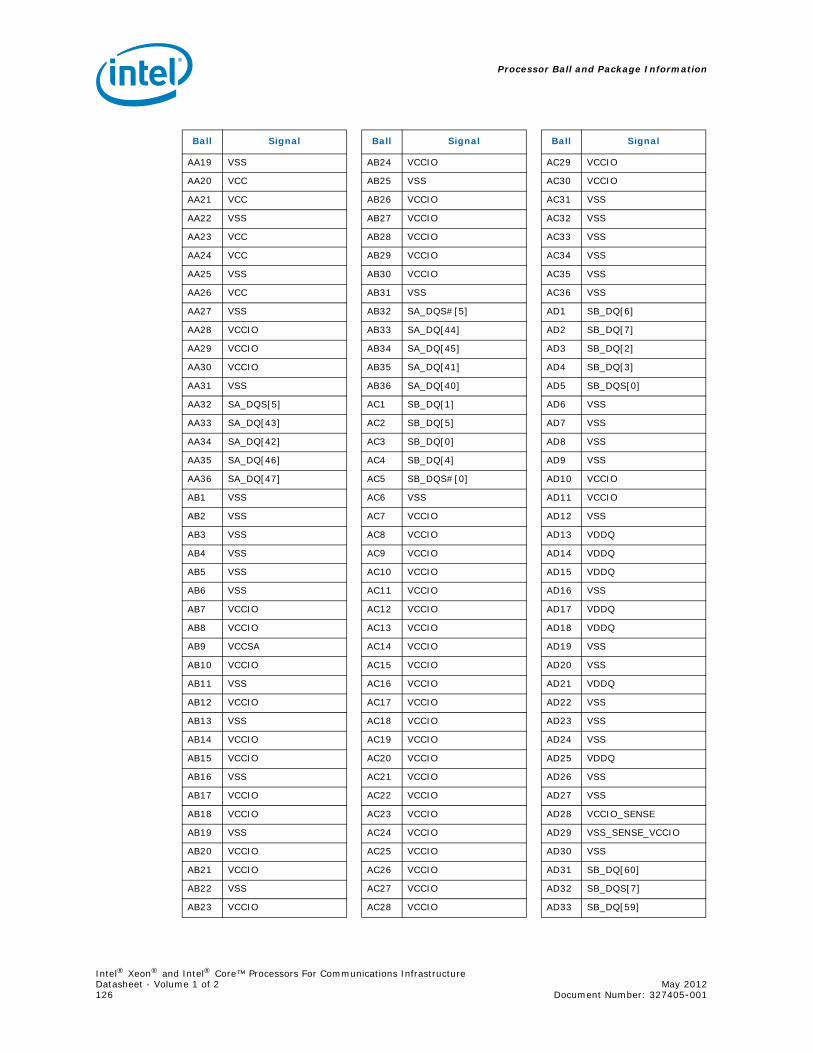
Intel® Xeon® and Intel® Core™ Processors For Communications InfrastructureDatasheet - Volume 1 of 2 May 2012126 Document Number: 327405-001
Processor Ball and Package Information
AA19 VSS
AA20 VCC
AA21 VCC
AA22 VSS
AA23 VCC
AA24 VCC
AA25 VSS
AA26 VCC
AA27 VSS
AA28 VCCIO
AA29 VCCIO
AA30 VCCIO
AA31 VSS
AA32 SA_DQS[5]
AA33 SA_DQ[43]
AA34 SA_DQ[42]
AA35 SA_DQ[46]
AA36 SA_DQ[47]
AB1 VSS
AB2 VSS
AB3 VSS
AB4 VSS
AB5 VSS
AB6 VSS
AB7 VCCIO
AB8 VCCIO
AB9 VCCSA
AB10 VCCIO
AB11 VSS
AB12 VCCIO
AB13 VSS
AB14 VCCIO
AB15 VCCIO
AB16 VSS
AB17 VCCIO
AB18 VCCIO
AB19 VSS
AB20 VCCIO
AB21 VCCIO
AB22 VSS
AB23 VCCIO
Ball Signal
AB24 VCCIO
AB25 VSS
AB26 VCCIO
AB27 VCCIO
AB28 VCCIO
AB29 VCCIO
AB30 VCCIO
AB31 VSS
AB32 SA_DQS#[5]
AB33 SA_DQ[44]
AB34 SA_DQ[45]
AB35 SA_DQ[41]
AB36 SA_DQ[40]
AC1 SB_DQ[1]
AC2 SB_DQ[5]
AC3 SB_DQ[0]
AC4 SB_DQ[4]
AC5 SB_DQS#[0]
AC6 VSS
AC7 VCCIO
AC8 VCCIO
AC9 VCCIO
AC10 VCCIO
AC11 VCCIO
AC12 VCCIO
AC13 VCCIO
AC14 VCCIO
AC15 VCCIO
AC16 VCCIO
AC17 VCCIO
AC18 VCCIO
AC19 VCCIO
AC20 VCCIO
AC21 VCCIO
AC22 VCCIO
AC23 VCCIO
AC24 VCCIO
AC25 VCCIO
AC26 VCCIO
AC27 VCCIO
AC28 VCCIO
Ball Signal
AC29 VCCIO
AC30 VCCIO
AC31 VSS
AC32 VSS
AC33 VSS
AC34 VSS
AC35 VSS
AC36 VSS
AD1 SB_DQ[6]
AD2 SB_DQ[7]
AD3 SB_DQ[2]
AD4 SB_DQ[3]
AD5 SB_DQS[0]
AD6 VSS
AD7 VSS
AD8 VSS
AD9 VSS
AD10 VCCIO
AD11 VCCIO
AD12 VSS
AD13 VDDQ
AD14 VDDQ
AD15 VDDQ
AD16 VSS
AD17 VDDQ
AD18 VDDQ
AD19 VSS
AD20 VSS
AD21 VDDQ
AD22 VSS
AD23 VSS
AD24 VSS
AD25 VDDQ
AD26 VSS
AD27 VSS
AD28 VCCIO_SENSE
AD29 VSS_SENSE_VCCIO
AD30 VSS
AD31 SB_DQ[60]
AD32 SB_DQS[7]
AD33 SB_DQ[59]
Ball Signal
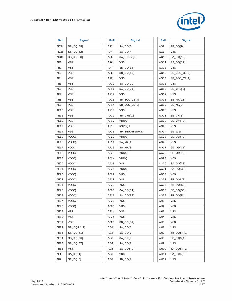
Intel® Xeon® and Intel® Core™ Processors For Communications InfrastructureMay 2012 Datasheet - Volume 1 of 2Document Number: 327405-001 127
Processor Ball and Package Information
AD34 SB_DQ[58]
AD35 SB_DQ[62]
AD36 SB_DQ[63]
AE1 VSS
AE2 VSS
AE3 VSS
AE4 VSS
AE5 VSS
AE6 VSS
AE7 VSS
AE8 VSS
AE9 VSS
AE10 VSS
AE11 VSS
AE12 VSS
AE13 VSS
AE14 VSS
AE15 VDDQ
AE16 VDDQ
AE17 VDDQ
AE18 VDDQ
AE19 VDDQ
AE20 VDDQ
AE21 VDDQ
AE22 VDDQ
AE23 VDDQ
AE24 VDDQ
AE25 VDDQ
AE26 VDDQ
AE27 VDDQ
AE28 VDDQ
AE29 VSS
AE30 VSS
AE31 VSS
AE32 SB_DQS#[7]
AE33 SB_DQ[61]
AE34 SB_DQ[56]
AE35 SB_DQ[57]
AE36 VSS
AF1 SA_DQ[1]
AF2 SA_DQ[5]
Ball Signal
AF3 SA_DQ[0]
AF4 SA_DQ[4]
AF5 SA_DQS#[0]
AF6 VSS
AF7 SB_DQ[12]
AF8 SB_DQ[13]
AF9 VSS
AF10 SA_DQ[20]
AF11 SA_DQ[21]
AF12 VSS
AF13 SB_ECC_CB[4]
AF14 SB_ECC_CB[5]
AF15 VSS
AF16 SB_CKE[2]
AF17 VDDQ
AF18 RSVD_1
AF19 SM_DRAMPWROK
AF20 VDDQ
AF21 SA_MA[4]
AF22 SA_MA[2]
AF23 VDDQ
AF24 VDDQ
AF25 VSS
AF26 VDDQ
AF27 VSS
AF28 VSS
AF29 VSS
AF30 SA_DQ[34]
AF31 SA_DQ[35]
AF32 VSS
AF33 VSS
AF34 VSS
AF35 VSS
AF36 SB_DQ[51]
AG1 SA_DQ[6]
AG2 SA_DQ[7]
AG3 SA_DQ[2]
AG4 SA_DQ[3]
AG5 SA_DQS[0]
AG6 VSS
AG7 SB_DQ[8]
Ball Signal
AG8 SB_DQ[9]
AG9 VSS
AG10 SA_DQ[16]
AG11 SA_DQ[17]
AG12 VSS
AG13 SB_ECC_CB[0]
AG14 SB_ECC_CB[1]
AG15 VSS
AG16 SB_CKE[1]
AG17 VSS
AG18 SB_MA[11]
AG19 SB_MA[7]
AG20 VSS
AG21 SB_CK[3]
AG22 SB_CK#[3]
AG23 VSS
AG24 SB_WE#
AG25 SB_CS#[0]
AG26 VSS
AG27 SB_ODT[1]
AG28 SB_ODT[3]
AG29 VSS
AG30 SA_DQ[38]
AG31 SA_DQ[39]
AG32 VSS
AG33 SB_DQS[6]
AG34 SB_DQ[50]
AG35 SB_DQ[55]
AG36 SB_DQ[54]
AH1 VSS
AH2 VSS
AH3 VSS
AH4 VSS
AH5 VSS
AH6 VSS
AH7 SB_DQS#[1]
AH8 SB_DQS[1]
AH9 VSS
AH10 SA_DQS#[2]
AH11 SA_DQS[2]
AH12 VSS
Ball Signal
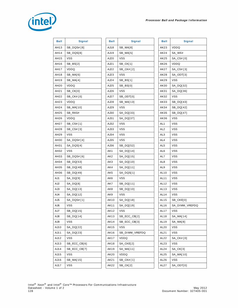
Intel® Xeon® and Intel® Core™ Processors For Communications InfrastructureDatasheet - Volume 1 of 2 May 2012128 Document Number: 327405-001
Processor Ball and Package Information
AH13 SB_DQS#[8]
AH14 SB_DQS[8]
AH15 VSS
AH16 SB_BS[2]
AH17 VDDQ
AH18 SB_MA[6]
AH19 SB_MA[4]
AH20 VDDQ
AH21 SB_CK[0]
AH22 SB_CK#[0]
AH23 VDDQ
AH24 SB_MA[10]
AH25 SB_RAS#
AH26 VDDQ
AH27 SB_CS#[1]
AH28 SB_CS#[3]
AH29 VSS
AH30 SA_DQS#[4]
AH31 SA_DQS[4]
AH32 VSS
AH33 SB_DQS#[6]
AH34 SB_DQ[53]
AH35 SB_DQ[48]
AH36 SB_DQ[49]
AJ1 SA_DQ[9]
AJ2 SA_DQ[8]
AJ3 SA_DQ[13]
AJ4 SA_DQ[12]
AJ5 SA_DQS#[1]
AJ6 VSS
AJ7 SB_DQ[15]
AJ8 SB_DQ[14]
AJ9 VSS
AJ10 SA_DQ[22]
AJ11 SA_DQ[23]
AJ12 VSS
AJ13 SB_ECC_CB[6]
AJ14 SB_ECC_CB[7]
AJ15 VSS
AJ16 SB_MA[15]
AJ17 VSS
Ball Signal
AJ18 SB_MA[8]
AJ19 SB_MA[5]
AJ20 VSS
AJ21 SB_CK[1]
AJ22 SB_CK#[2]
AJ23 VSS
AJ24 SB_BS[1]
AJ25 SB_BS[0]
AJ26 VSS
AJ27 SB_ODT[0]
AJ28 SB_MA[13]
AJ29 VSS
AJ30 SA_DQ[33]
AJ31 SA_DQ[37]
AJ32 VSS
AJ33 VSS
AJ34 VSS
AJ35 VSS
AJ36 SB_DQ[52]
AK1 SA_DQ[14]
AK2 SA_DQ[15]
AK3 SA_DQ[10]
AK4 SA_DQ[11]
AK5 SA_DQS[1]
AK6 VSS
AK7 SB_DQ[11]
AK8 SB_DQ[10]
AK9 VSS
AK10 SA_DQ[18]
AK11 SA_DQ[19]
AK12 VSS
AK13 SB_ECC_CB[2]
AK14 SB_ECC_CB[3]
AK15 VSS
AK16 SB_DIMM_VREFDQ
AK17 VDDQ
AK18 SA_CKE[2]
AK19 SA_MA[11]
AK20 VDDQ
AK21 SB_CK#[1]
AK22 SB_CK[2]
Ball Signal
AK23 VDDQ
AK24 SA_WE#
AK25 SA_CS#[0]
AK26 VDDQ
AK27 SA_CS#[3]
AK28 SA_ODT[3]
AK29 VSS
AK30 SA_DQ[32]
AK31 SA_DQ[36]
AK32 VSS
AK33 SB_DQ[43]
AK34 SB_DQ[42]
AK35 SB_DQ[47]
AK36 VSS
AL1 VSS
AL2 VSS
AL3 VSS
AL4 VSS
AL5 VSS
AL6 VSS
AL7 VSS
AL8 VSS
AL9 VSS
AL10 VSS
AL11 VSS
AL12 VSS
AL13 VSS
AL14 VSS
AL15 SB_CKE[0]
AL16 SA_DIMM_VREFDQ
AL17 VSS
AL18 SA_MA[14]
AL19 SA_MA[8]
AL20 VSS
AL21 VSS
AL22 SA_CK#[0]
AL23 VSS
AL24 SA_CK[3]
AL25 SA_MA[10]
AL26 VSS
AL27 SA_ODT[0]
Ball Signal
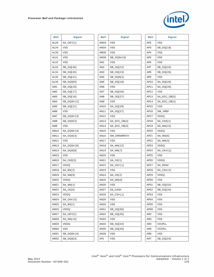
Intel® Xeon® and Intel® Core™ Processors For Communications InfrastructureMay 2012 Datasheet - Volume 1 of 2Document Number: 327405-001 129
Processor Ball and Package Information
AL28 SA_ODT[1]
AL29 VSS
AL30 VSS
AL31 VSS
AL32 VSS
AL33 SB_DQ[46]
AL34 SB_DQ[45]
AL35 SB_DQ[41]
AL36 SB_DQS[5]
AM1 SB_DQ[20]
AM2 SB_DQ[17]
AM3 SB_DQ[16]
AM4 SB_DQS#[2]
AM5 SB_DQ[21]
AM6 VSS
AM7 SB_DQS#[3]
AM8 SB_DQS[3]
AM9 VSS
AM10 SA_DQS#[3]
AM11 SA_DQS[3]
AM12 VSS
AM13 SA_DQS#[8]
AM14 SA_DQS[8]
AM15 VSS
AM16 SA_CKE[3]
AM17 VDDQ
AM18 SA_BS[2]
AM19 SA_MA[9]
AM20 VDDQ
AM21 SA_MA[1]
AM22 SA_CK[0]
AM23 VDDQ
AM24 SA_CK#[3]
AM25 SA_BS[1]
AM26 VDDQ
AM27 SA_ODT[2]
AM28 SA_MA[13]
AM29 VDDQ
AM30 VSS
AM31 SB_DQS#[4]
AM32 SB_DQS[4]
Ball Signal
AM33 VSS
AM34 VSS
AM35 VSS
AM36 SB_DQS#[5]
AN1 VSS
AN2 SB_DQ[22]
AN3 SB_DQ[23]
AN4 SB_DQS[2]
AN5 SB_DQ[19]
AN6 VSS
AN7 SB_DQ[28]
AN8 SB_DQ[27]
AN9 VSS
AN10 SA_DQ[28]
AN11 SA_DQ[27]
AN12 VSS
AN13 SA_ECC_CB[4]
AN14 SA_ECC_CB[3]
AN15 VSS
AN16 SM_DRAMRST#
AN17 VSS
AN18 SA_MA[12]
AN19 SA_MA[7]
AN20 VSS
AN21 SA_CK[1]
AN22 SA_CK#[1]
AN23 VSS
AN24 SA_CK[2]
AN25 SA_MA[0]
AN26 VSS
AN27 SA_CAS#
AN28 SA_CS#[1]
AN29 VSS
AN30 VSS
AN31 SB_DQ[36]
AN32 SB_DQ[35]
AN33 VSS
AN34 SB_DQ[44]
AN35 SB_DQ[40]
AN36 VSS
AP1 VSS
Ball Signal
AP2 VSS
AP3 SB_DQ[18]
AP4 VSS
AP5 VSS
AP6 VSS
AP7 SB_DQ[29]
AP8 SB_DQ[26]
AP9 VSS
AP10 SA_DQ[29]
AP11 SA_DQ[26]
AP12 VSS
AP13 SA_ECC_CB[5]
AP14 SA_ECC_CB[2]
AP15 VSS
AP16 SM_VREF
AP17 VDDQ
AP18 SA_CKE[1]
AP19 SA_MA[15]
AP20 VDDQ
AP21 SA_MA[6]
AP22 SA_MA[3]
AP23 VDDQ
AP24 SA_CK#[2]
AP25 VSS
AP26 VDDQ
AP27 SA_RAS#
AP28 SA_CS#[2]
AP29 VDDQ
AP30 VSS
AP31 SB_DQ[32]
AP32 SB_DQ[34]
AP33 VSS
AP34 VSS
AP35 VSS
AP36 VSS
AR2 VSS
AR3 VSS
AR4 VCCPLL
AR5 VCCPLL
AR6 VSS
AR7 SB_DQ[24]
Ball Signal
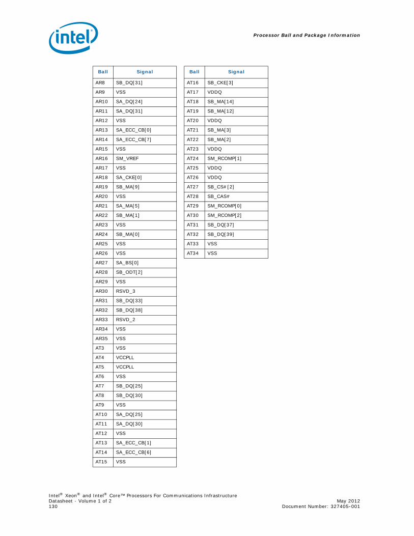
Intel® Xeon® and Intel® Core™ Processors For Communications InfrastructureDatasheet - Volume 1 of 2 May 2012130 Document Number: 327405-001
Processor Ball and Package Information
AR8 SB_DQ[31]
AR9 VSS
AR10 SA_DQ[24]
AR11 SA_DQ[31]
AR12 VSS
AR13 SA_ECC_CB[0]
AR14 SA_ECC_CB[7]
AR15 VSS
AR16 SM_VREF
AR17 VSS
AR18 SA_CKE[0]
AR19 SB_MA[9]
AR20 VSS
AR21 SA_MA[5]
AR22 SB_MA[1]
AR23 VSS
AR24 SB_MA[0]
AR25 VSS
AR26 VSS
AR27 SA_BS[0]
AR28 SB_ODT[2]
AR29 VSS
AR30 RSVD_3
AR31 SB_DQ[33]
AR32 SB_DQ[38]
AR33 RSVD_2
AR34 VSS
AR35 VSS
AT3 VSS
AT4 VCCPLL
AT5 VCCPLL
AT6 VSS
AT7 SB_DQ[25]
AT8 SB_DQ[30]
AT9 VSS
AT10 SA_DQ[25]
AT11 SA_DQ[30]
AT12 VSS
AT13 SA_ECC_CB[1]
AT14 SA_ECC_CB[6]
AT15 VSS
Ball Signal
AT16 SB_CKE[3]
AT17 VDDQ
AT18 SB_MA[14]
AT19 SB_MA[12]
AT20 VDDQ
AT21 SB_MA[3]
AT22 SB_MA[2]
AT23 VDDQ
AT24 SM_RCOMP[1]
AT25 VDDQ
AT26 VDDQ
AT27 SB_CS#[2]
AT28 SB_CAS#
AT29 SM_RCOMP[0]
AT30 SM_RCOMP[2]
AT31 SB_DQ[37]
AT32 SB_DQ[39]
AT33 VSS
AT34 VSS
Ball Signal
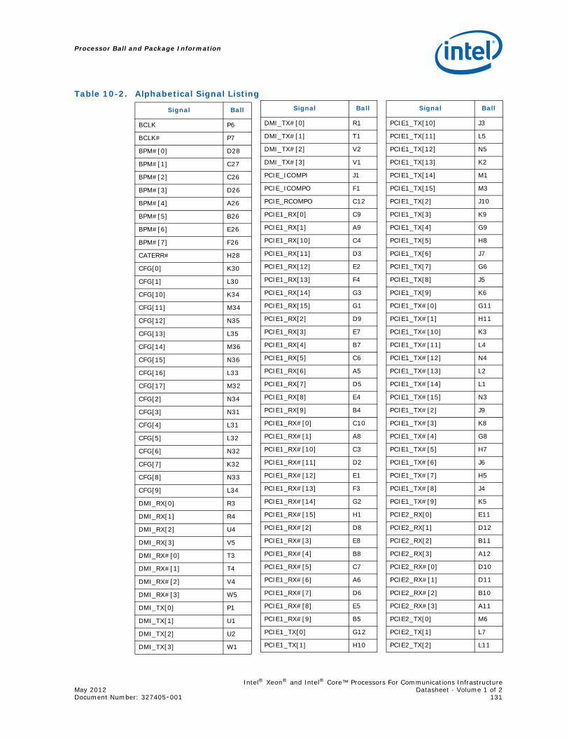
Intel® Xeon® and Intel® Core™ Processors For Communications InfrastructureMay 2012 Datasheet - Volume 1 of 2Document Number: 327405-001 131
Processor Ball and Package Information
Table 10-2. Alphabetical Signal Listing
Signal Ball
BCLK P6
BCLK# P7
BPM#[0] D28
BPM#[1] C27
BPM#[2] C26
BPM#[3] D26
BPM#[4] A26
BPM#[5] B26
BPM#[6] E26
BPM#[7] F26
CATERR# H28
CFG[0] K30
CFG[1] L30
CFG[10] K34
CFG[11] M34
CFG[12] N35
CFG[13] L35
CFG[14] M36
CFG[15] N36
CFG[16] L33
CFG[17] M32
CFG[2] N34
CFG[3] N31
CFG[4] L31
CFG[5] L32
CFG[6] N32
CFG[7] K32
CFG[8] N33
CFG[9] L34
DMI_RX[0] R3
DMI_RX[1] R4
DMI_RX[2] U4
DMI_RX[3] V5
DMI_RX#[0] T3
DMI_RX#[1] T4
DMI_RX#[2] V4
DMI_RX#[3] W5
DMI_TX[0] P1
DMI_TX[1] U1
DMI_TX[2] U2
DMI_TX[3] W1
DMI_TX#[0] R1
DMI_TX#[1] T1
DMI_TX#[2] V2
DMI_TX#[3] V1
PCIE_ICOMPI J1
PCIE_ICOMPO F1
PCIE_RCOMPO C12
PCIE1_RX[0] C9
PCIE1_RX[1] A9
PCIE1_RX[10] C4
PCIE1_RX[11] D3
PCIE1_RX[12] E2
PCIE1_RX[13] F4
PCIE1_RX[14] G3
PCIE1_RX[15] G1
PCIE1_RX[2] D9
PCIE1_RX[3] E7
PCIE1_RX[4] B7
PCIE1_RX[5] C6
PCIE1_RX[6] A5
PCIE1_RX[7] D5
PCIE1_RX[8] E4
PCIE1_RX[9] B4
PCIE1_RX#[0] C10
PCIE1_RX#[1] A8
PCIE1_RX#[10] C3
PCIE1_RX#[11] D2
PCIE1_RX#[12] E1
PCIE1_RX#[13] F3
PCIE1_RX#[14] G2
PCIE1_RX#[15] H1
PCIE1_RX#[2] D8
PCIE1_RX#[3] E8
PCIE1_RX#[4] B8
PCIE1_RX#[5] C7
PCIE1_RX#[6] A6
PCIE1_RX#[7] D6
PCIE1_RX#[8] E5
PCIE1_RX#[9] B5
PCIE1_TX[0] G12
PCIE1_TX[1] H10
Signal Ball
PCIE1_TX[10] J3
PCIE1_TX[11] L5
PCIE1_TX[12] N5
PCIE1_TX[13] K2
PCIE1_TX[14] M1
PCIE1_TX[15] M3
PCIE1_TX[2] J10
PCIE1_TX[3] K9
PCIE1_TX[4] G9
PCIE1_TX[5] H8
PCIE1_TX[6] J7
PCIE1_TX[7] G6
PCIE1_TX[8] J5
PCIE1_TX[9] K6
PCIE1_TX#[0] G11
PCIE1_TX#[1] H11
PCIE1_TX#[10] K3
PCIE1_TX#[11] L4
PCIE1_TX#[12] N4
PCIE1_TX#[13] L2
PCIE1_TX#[14] L1
PCIE1_TX#[15] N3
PCIE1_TX#[2] J9
PCIE1_TX#[3] K8
PCIE1_TX#[4] G8
PCIE1_TX#[5] H7
PCIE1_TX#[6] J6
PCIE1_TX#[7] H5
PCIE1_TX#[8] J4
PCIE1_TX#[9] K5
PCIE2_RX[0] E11
PCIE2_RX[1] D12
PCIE2_RX[2] B11
PCIE2_RX[3] A12
PCIE2_RX#[0] D10
PCIE2_RX#[1] D11
PCIE2_RX#[2] B10
PCIE2_RX#[3] A11
PCIE2_TX[0] M6
PCIE2_TX[1] L7
PCIE2_TX[2] L11
Signal Ball
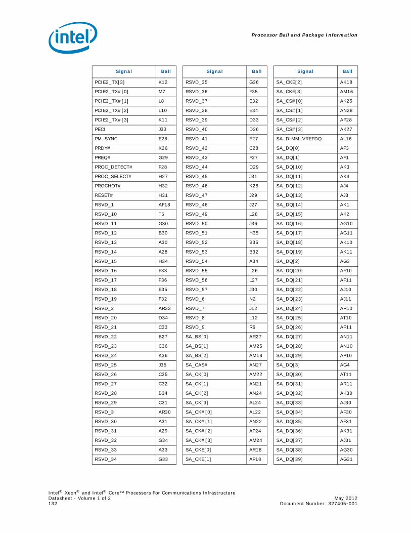
Intel® Xeon® and Intel® Core™ Processors For Communications InfrastructureDatasheet - Volume 1 of 2 May 2012132 Document Number: 327405-001
Processor Ball and Package Information
PCIE2_TX[3] K12
PCIE2_TX#[0] M7
PCIE2_TX#[1] L8
PCIE2_TX#[2] L10
PCIE2_TX#[3] K11
PECI J33
PM_SYNC E28
PRDY# K26
PREQ# G29
PROC_DETECT# F28
PROC_SELECT# H27
PROCHOT# H32
RESET# H31
RSVD_1 AF18
RSVD_10 T6
RSVD_11 G30
RSVD_12 B30
RSVD_13 A30
RSVD_14 A28
RSVD_15 H34
RSVD_16 F33
RSVD_17 F36
RSVD_18 E35
RSVD_19 F32
RSVD_2 AR33
RSVD_20 D34
RSVD_21 C33
RSVD_22 B27
RSVD_23 C36
RSVD_24 K36
RSVD_25 J35
RSVD_26 C35
RSVD_27 C32
RSVD_28 B34
RSVD_29 C31
RSVD_3 AR30
RSVD_30 A31
RSVD_31 A29
RSVD_32 G34
RSVD_33 A33
RSVD_34 G33
Signal Ball
RSVD_35 G36
RSVD_36 F35
RSVD_37 E32
RSVD_38 E34
RSVD_39 D33
RSVD_40 D36
RSVD_41 E27
RSVD_42 C28
RSVD_43 F27
RSVD_44 D29
RSVD_45 J31
RSVD_46 K28
RSVD_47 J29
RSVD_48 J27
RSVD_49 L28
RSVD_50 J36
RSVD_51 H35
RSVD_52 B35
RSVD_53 B32
RSVD_54 A34
RSVD_55 L26
RSVD_56 L27
RSVD_57 J30
RSVD_6 N2
RSVD_7 J12
RSVD_8 L12
RSVD_9 R6
SA_BS[0] AR27
SA_BS[1] AM25
SA_BS[2] AM18
SA_CAS# AN27
SA_CK[0] AM22
SA_CK[1] AN21
SA_CK[2] AN24
SA_CK[3] AL24
SA_CK#[0] AL22
SA_CK#[1] AN22
SA_CK#[2] AP24
SA_CK#[3] AM24
SA_CKE[0] AR18
SA_CKE[1] AP18
Signal Ball
SA_CKE[2] AK18
SA_CKE[3] AM16
SA_CS#[0] AK25
SA_CS#[1] AN28
SA_CS#[2] AP28
SA_CS#[3] AK27
SA_DIMM_VREFDQ AL16
SA_DQ[0] AF3
SA_DQ[1] AF1
SA_DQ[10] AK3
SA_DQ[11] AK4
SA_DQ[12] AJ4
SA_DQ[13] AJ3
SA_DQ[14] AK1
SA_DQ[15] AK2
SA_DQ[16] AG10
SA_DQ[17] AG11
SA_DQ[18] AK10
SA_DQ[19] AK11
SA_DQ[2] AG3
SA_DQ[20] AF10
SA_DQ[21] AF11
SA_DQ[22] AJ10
SA_DQ[23] AJ11
SA_DQ[24] AR10
SA_DQ[25] AT10
SA_DQ[26] AP11
SA_DQ[27] AN11
SA_DQ[28] AN10
SA_DQ[29] AP10
SA_DQ[3] AG4
SA_DQ[30] AT11
SA_DQ[31] AR11
SA_DQ[32] AK30
SA_DQ[33] AJ30
SA_DQ[34] AF30
SA_DQ[35] AF31
SA_DQ[36] AK31
SA_DQ[37] AJ31
SA_DQ[38] AG30
SA_DQ[39] AG31
Signal Ball
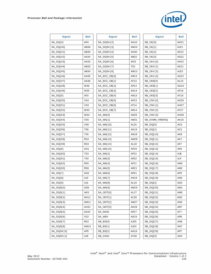
Intel® Xeon® and Intel® Core™ Processors For Communications InfrastructureMay 2012 Datasheet - Volume 1 of 2Document Number: 327405-001 133
Processor Ball and Package Information
SA_DQ[4] AF4
SA_DQ[40] AB36
SA_DQ[41] AB35
SA_DQ[42] AA34
SA_DQ[43] AA33
SA_DQ[44] AB33
SA_DQ[45] AB34
SA_DQ[46] AA35
SA_DQ[47] AA36
SA_DQ[48] W36
SA_DQ[49] W35
SA_DQ[5] AF2
SA_DQ[50] V34
SA_DQ[51] V33
SA_DQ[52] W33
SA_DQ[53] W34
SA_DQ[54] V35
SA_DQ[55] V36
SA_DQ[56] T36
SA_DQ[57] T35
SA_DQ[58] R34
SA_DQ[59] R33
SA_DQ[6] AG1
SA_DQ[60] T33
SA_DQ[61] T34
SA_DQ[62] R35
SA_DQ[63] R36
SA_DQ[7] AG2
SA_DQ[8] AJ2
SA_DQ[9] AJ1
SA_DQS[0] AG5
SA_DQS[1] AK5
SA_DQS[2] AH11
SA_DQS[3] AM11
SA_DQS[4] AH31
SA_DQS[5] AA32
SA_DQS[6] V32
SA_DQS[7] R32
SA_DQS[8] AM14
SA_DQS#[0] AF5
SA_DQS#[1] AJ5
Signal Ball
SA_DQS#[2] AH10
SA_DQS#[3] AM10
SA_DQS#[4] AH30
SA_DQS#[5] AB32
SA_DQS#[6] W32
SA_DQS#[7] T32
SA_DQS#[8] AM13
SA_ECC_CB[0] AR13
SA_ECC_CB[1] AT13
SA_ECC_CB[2] AP14
SA_ECC_CB[3] AN14
SA_ECC_CB[4] AN13
SA_ECC_CB[5] AP13
SA_ECC_CB[6] AT14
SA_ECC_CB[7] AR14
SA_MA[0] AN25
SA_MA[1] AM21
SA_MA[10] AL25
SA_MA[11] AK19
SA_MA[12] AN18
SA_MA[13] AM28
SA_MA[14] AL18
SA_MA[15] AP19
SA_MA[2] AF22
SA_MA[3] AP22
SA_MA[4] AF21
SA_MA[5] AR21
SA_MA[6] AP21
SA_MA[7] AN19
SA_MA[8] AL19
SA_MA[9] AM19
SA_ODT[0] AL27
SA_ODT[1] AL28
SA_ODT[2] AM27
SA_ODT[3] AK28
SA_RAS# AP27
SA_WE# AK24
SB_BS[0] AJ25
SB_BS[1] AJ24
SB_BS[2] AH16
SB_CAS# AT28
Signal Ball
SB_CK[0] AH21
SB_CK[1] AJ21
SB_CK[2] AK22
SB_CK[3] AG21
SB_CK#[0] AH22
SB_CK#[1] AK21
SB_CK#[2] AJ22
SB_CK#[3] AG22
SB_CKE[0] AL15
SB_CKE[1] AG16
SB_CKE[2] AF16
SB_CKE[3] AT16
SB_CS#[0] AG25
SB_CS#[1] AH27
SB_CS#[2] AT27
SB_CS#[3] AH28
SB_DIMM_VREFDQ AK16
SB_DQ[0] AC3
SB_DQ[1] AC1
SB_DQ[10] AK8
SB_DQ[11] AK7
SB_DQ[12] AF7
SB_DQ[13] AF8
SB_DQ[14] AJ8
SB_DQ[15] AJ7
SB_DQ[16] AM3
SB_DQ[17] AM2
SB_DQ[18] AP3
SB_DQ[19] AN5
SB_DQ[2] AD3
SB_DQ[20] AM1
SB_DQ[21] AM5
SB_DQ[22] AN2
SB_DQ[23] AN3
SB_DQ[24] AR7
SB_DQ[25] AT7
SB_DQ[26] AP8
SB_DQ[27] AN8
SB_DQ[28] AN7
SB_DQ[29] AP7
SB_DQ[3] AD4
Signal Ball
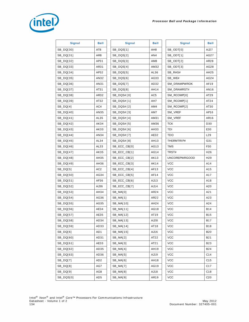
Intel® Xeon® and Intel® Core™ Processors For Communications InfrastructureDatasheet - Volume 1 of 2 May 2012134 Document Number: 327405-001
Processor Ball and Package Information
SB_DQ[30] AT8
SB_DQ[31] AR8
SB_DQ[32] AP31
SB_DQ[33] AR31
SB_DQ[34] AP32
SB_DQ[35] AN32
SB_DQ[36] AN31
SB_DQ[37] AT31
SB_DQ[38] AR32
SB_DQ[39] AT32
SB_DQ[4] AC4
SB_DQ[40] AN35
SB_DQ[41] AL35
SB_DQ[42] AK34
SB_DQ[43] AK33
SB_DQ[44] AN34
SB_DQ[45] AL34
SB_DQ[46] AL33
SB_DQ[47] AK35
SB_DQ[48] AH35
SB_DQ[49] AH36
SB_DQ[5] AC2
SB_DQ[50] AG34
SB_DQ[51] AF36
SB_DQ[52] AJ36
SB_DQ[53] AH34
SB_DQ[54] AG36
SB_DQ[55] AG35
SB_DQ[56] AE34
SB_DQ[57] AE35
SB_DQ[58] AD34
SB_DQ[59] AD33
SB_DQ[6] AD1
SB_DQ[60] AD31
SB_DQ[61] AE33
SB_DQ[62] AD35
SB_DQ[63] AD36
SB_DQ[7] AD2
SB_DQ[8] AG7
SB_DQ[9] AG8
SB_DQS[0] AD5
Signal Ball
SB_DQS[1] AH8
SB_DQS[2] AN4
SB_DQS[3] AM8
SB_DQS[4] AM32
SB_DQS[5] AL36
SB_DQS[6] AG33
SB_DQS[7] AD32
SB_DQS[8] AH14
SB_DQS#[0] AC5
SB_DQS#[1] AH7
SB_DQS#[2] AM4
SB_DQS#[3] AM7
SB_DQS#[4] AM31
SB_DQS#[5] AM36
SB_DQS#[6] AH33
SB_DQS#[7] AE32
SB_DQS#[8] AH13
SB_ECC_CB[0] AG13
SB_ECC_CB[1] AG14
SB_ECC_CB[2] AK13
SB_ECC_CB[3] AK14
SB_ECC_CB[4] AF13
SB_ECC_CB[5] AF14
SB_ECC_CB[6] AJ13
SB_ECC_CB[7] AJ14
SB_MA[0] AR24
SB_MA[1] AR22
SB_MA[10] AH24
SB_MA[11] AG18
SB_MA[12] AT19
SB_MA[13] AJ28
SB_MA[14] AT18
SB_MA[15] AJ16
SB_MA[2] AT22
SB_MA[3] AT21
SB_MA[4] AH19
SB_MA[5] AJ19
SB_MA[6] AH18
SB_MA[7] AG19
SB_MA[8] AJ18
SB_MA[9] AR19
Signal Ball
SB_ODT[0] AJ27
SB_ODT[1] AG27
SB_ODT[2] AR28
SB_ODT[3] AG28
SB_RAS# AH25
SB_WE# AG24
SM_DRAMPWROK AF19
SM_DRAMRST# AN16
SM_RCOMP[0] AT29
SM_RCOMP[1] AT24
SM_RCOMP[2] AT30
SM_VREF AP16
SM_VREF AR16
TCK D30
TDI E30
TDO L29
THERMTRIP# G31
TMS F30
TRST# H26
UNCOREPWRGOOD H29
VCC A14
VCC A15
VCC A17
VCC A18
VCC A20
VCC A21
VCC A23
VCC A24
VCC B14
VCC B15
VCC B17
VCC B18
VCC B20
VCC B21
VCC B23
VCC B24
VCC C14
VCC C15
VCC C17
VCC C18
VCC C20
Signal Ball
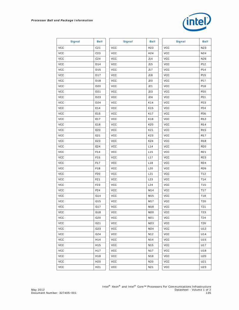
Intel® Xeon® and Intel® Core™ Processors For Communications InfrastructureMay 2012 Datasheet - Volume 1 of 2Document Number: 327405-001 135
Processor Ball and Package Information
VCC C21
VCC C23
VCC C24
VCC D14
VCC D15
VCC D17
VCC D18
VCC D20
VCC D21
VCC D23
VCC D24
VCC E14
VCC E15
VCC E17
VCC E18
VCC E20
VCC E21
VCC E23
VCC E24
VCC F14
VCC F15
VCC F17
VCC F18
VCC F20
VCC F21
VCC F23
VCC F24
VCC G14
VCC G15
VCC G17
VCC G18
VCC G20
VCC G21
VCC G23
VCC G24
VCC H14
VCC H15
VCC H17
VCC H18
VCC H20
VCC H21
Signal Ball
VCC H23
VCC H24
VCC J14
VCC J15
VCC J17
VCC J18
VCC J20
VCC J21
VCC J23
VCC J24
VCC K14
VCC K15
VCC K17
VCC K18
VCC K20
VCC K21
VCC K23
VCC K24
VCC L14
VCC L15
VCC L17
VCC L18
VCC L20
VCC L21
VCC L23
VCC L24
VCC M14
VCC M15
VCC M17
VCC M18
VCC M20
VCC M21
VCC M23
VCC M24
VCC N12
VCC N14
VCC N15
VCC N17
VCC N18
VCC N20
VCC N21
Signal Ball
VCC N23
VCC N24
VCC N26
VCC P12
VCC P14
VCC P15
VCC P17
VCC P18
VCC P20
VCC P21
VCC P23
VCC P24
VCC P26
VCC R12
VCC R14
VCC R15
VCC R17
VCC R18
VCC R20
VCC R21
VCC R23
VCC R24
VCC R26
VCC T12
VCC T14
VCC T15
VCC T17
VCC T18
VCC T20
VCC T21
VCC T23
VCC T24
VCC T26
VCC U12
VCC U14
VCC U15
VCC U17
VCC U18
VCC U20
VCC U21
VCC U23
Signal Ball
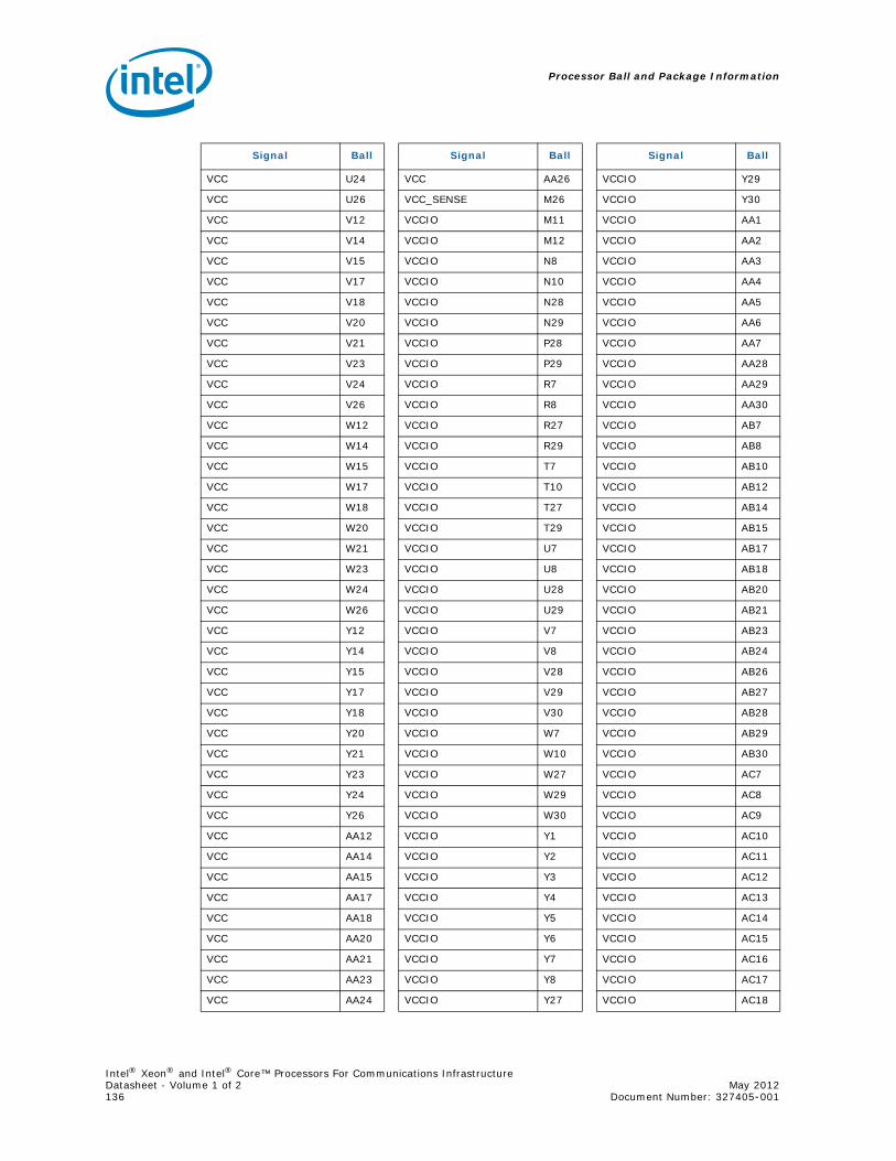
Intel® Xeon® and Intel® Core™ Processors For Communications InfrastructureDatasheet - Volume 1 of 2 May 2012136 Document Number: 327405-001
Processor Ball and Package Information
VCC U24
VCC U26
VCC V12
VCC V14
VCC V15
VCC V17
VCC V18
VCC V20
VCC V21
VCC V23
VCC V24
VCC V26
VCC W12
VCC W14
VCC W15
VCC W17
VCC W18
VCC W20
VCC W21
VCC W23
VCC W24
VCC W26
VCC Y12
VCC Y14
VCC Y15
VCC Y17
VCC Y18
VCC Y20
VCC Y21
VCC Y23
VCC Y24
VCC Y26
VCC AA12
VCC AA14
VCC AA15
VCC AA17
VCC AA18
VCC AA20
VCC AA21
VCC AA23
VCC AA24
Signal Ball
VCC AA26
VCC_SENSE M26
VCCIO M11
VCCIO M12
VCCIO N8
VCCIO N10
VCCIO N28
VCCIO N29
VCCIO P28
VCCIO P29
VCCIO R7
VCCIO R8
VCCIO R27
VCCIO R29
VCCIO T7
VCCIO T10
VCCIO T27
VCCIO T29
VCCIO U7
VCCIO U8
VCCIO U28
VCCIO U29
VCCIO V7
VCCIO V8
VCCIO V28
VCCIO V29
VCCIO V30
VCCIO W7
VCCIO W10
VCCIO W27
VCCIO W29
VCCIO W30
VCCIO Y1
VCCIO Y2
VCCIO Y3
VCCIO Y4
VCCIO Y5
VCCIO Y6
VCCIO Y7
VCCIO Y8
VCCIO Y27
Signal Ball
VCCIO Y29
VCCIO Y30
VCCIO AA1
VCCIO AA2
VCCIO AA3
VCCIO AA4
VCCIO AA5
VCCIO AA6
VCCIO AA7
VCCIO AA28
VCCIO AA29
VCCIO AA30
VCCIO AB7
VCCIO AB8
VCCIO AB10
VCCIO AB12
VCCIO AB14
VCCIO AB15
VCCIO AB17
VCCIO AB18
VCCIO AB20
VCCIO AB21
VCCIO AB23
VCCIO AB24
VCCIO AB26
VCCIO AB27
VCCIO AB28
VCCIO AB29
VCCIO AB30
VCCIO AC7
VCCIO AC8
VCCIO AC9
VCCIO AC10
VCCIO AC11
VCCIO AC12
VCCIO AC13
VCCIO AC14
VCCIO AC15
VCCIO AC16
VCCIO AC17
VCCIO AC18
Signal Ball
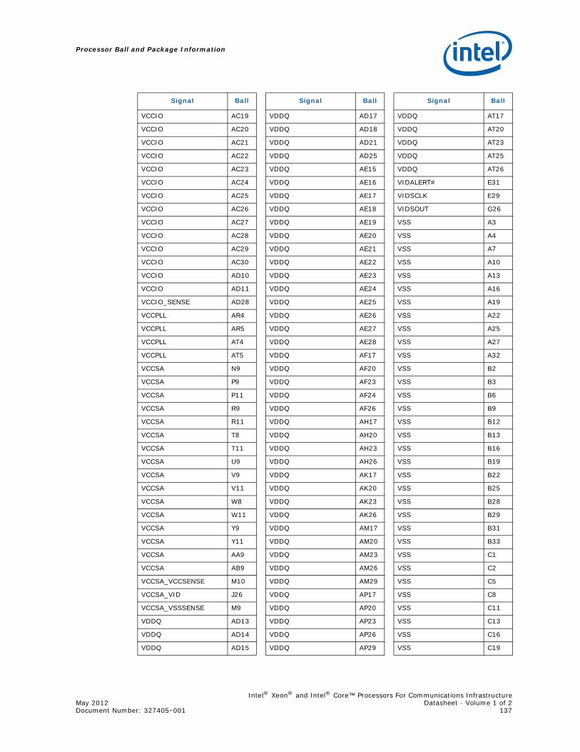
Intel® Xeon® and Intel® Core™ Processors For Communications InfrastructureMay 2012 Datasheet - Volume 1 of 2Document Number: 327405-001 137
Processor Ball and Package Information
VCCIO AC19
VCCIO AC20
VCCIO AC21
VCCIO AC22
VCCIO AC23
VCCIO AC24
VCCIO AC25
VCCIO AC26
VCCIO AC27
VCCIO AC28
VCCIO AC29
VCCIO AC30
VCCIO AD10
VCCIO AD11
VCCIO_SENSE AD28
VCCPLL AR4
VCCPLL AR5
VCCPLL AT4
VCCPLL AT5
VCCSA N9
VCCSA P9
VCCSA P11
VCCSA R9
VCCSA R11
VCCSA T8
VCCSA T11
VCCSA U9
VCCSA V9
VCCSA V11
VCCSA W8
VCCSA W11
VCCSA Y9
VCCSA Y11
VCCSA AA9
VCCSA AB9
VCCSA_VCCSENSE M10
VCCSA_VID J26
VCCSA_VSSSENSE M9
VDDQ AD13
VDDQ AD14
VDDQ AD15
Signal Ball
VDDQ AD17
VDDQ AD18
VDDQ AD21
VDDQ AD25
VDDQ AE15
VDDQ AE16
VDDQ AE17
VDDQ AE18
VDDQ AE19
VDDQ AE20
VDDQ AE21
VDDQ AE22
VDDQ AE23
VDDQ AE24
VDDQ AE25
VDDQ AE26
VDDQ AE27
VDDQ AE28
VDDQ AF17
VDDQ AF20
VDDQ AF23
VDDQ AF24
VDDQ AF26
VDDQ AH17
VDDQ AH20
VDDQ AH23
VDDQ AH26
VDDQ AK17
VDDQ AK20
VDDQ AK23
VDDQ AK26
VDDQ AM17
VDDQ AM20
VDDQ AM23
VDDQ AM26
VDDQ AM29
VDDQ AP17
VDDQ AP20
VDDQ AP23
VDDQ AP26
VDDQ AP29
Signal Ball
VDDQ AT17
VDDQ AT20
VDDQ AT23
VDDQ AT25
VDDQ AT26
VIDALERT# E31
VIDSCLK E29
VIDSOUT G26
VSS A3
VSS A4
VSS A7
VSS A10
VSS A13
VSS A16
VSS A19
VSS A22
VSS A25
VSS A27
VSS A32
VSS B2
VSS B3
VSS B6
VSS B9
VSS B12
VSS B13
VSS B16
VSS B19
VSS B22
VSS B25
VSS B28
VSS B29
VSS B31
VSS B33
VSS C1
VSS C2
VSS C5
VSS C8
VSS C11
VSS C13
VSS C16
VSS C19
Signal Ball
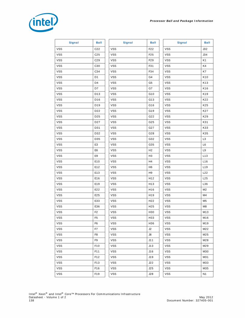
Intel® Xeon® and Intel® Core™ Processors For Communications InfrastructureDatasheet - Volume 1 of 2 May 2012138 Document Number: 327405-001
Processor Ball and Package Information
VSS C22
VSS C25
VSS C29
VSS C30
VSS C34
VSS D1
VSS D4
VSS D7
VSS D13
VSS D16
VSS D19
VSS D22
VSS D25
VSS D27
VSS D31
VSS D32
VSS D35
VSS E3
VSS E6
VSS E9
VSS E10
VSS E12
VSS E13
VSS E16
VSS E19
VSS E22
VSS E25
VSS E33
VSS E36
VSS F2
VSS F5
VSS F6
VSS F7
VSS F8
VSS F9
VSS F10
VSS F11
VSS F12
VSS F13
VSS F16
VSS F19
Signal Ball
VSS F22
VSS F25
VSS F29
VSS F31
VSS F34
VSS G4
VSS G5
VSS G7
VSS G10
VSS G13
VSS G16
VSS G19
VSS G22
VSS G25
VSS G27
VSS G28
VSS G32
VSS G35
VSS H2
VSS H3
VSS H4
VSS H6
VSS H9
VSS H12
VSS H13
VSS H16
VSS H19
VSS H22
VSS H25
VSS H30
VSS H33
VSS H36
VSS J2
VSS J8
VSS J11
VSS J13
VSS J16
VSS J19
VSS J22
VSS J25
VSS J28
Signal Ball
VSS J32
VSS J34
VSS K1
VSS K4
VSS K7
VSS K10
VSS K13
VSS K16
VSS K19
VSS K22
VSS K25
VSS K27
VSS K29
VSS K31
VSS K33
VSS K35
VSS L3
VSS L6
VSS L9
VSS L13
VSS L16
VSS L19
VSS L22
VSS L25
VSS L36
VSS M2
VSS M4
VSS M5
VSS M8
VSS M13
VSS M16
VSS M19
VSS M22
VSS M25
VSS M28
VSS M29
VSS M30
VSS M31
VSS M33
VSS M35
VSS N1
Signal Ball
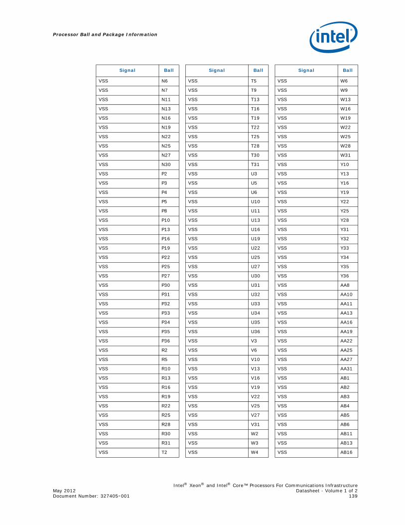
Intel® Xeon® and Intel® Core™ Processors For Communications InfrastructureMay 2012 Datasheet - Volume 1 of 2Document Number: 327405-001 139
Processor Ball and Package Information
VSS N6
VSS N7
VSS N11
VSS N13
VSS N16
VSS N19
VSS N22
VSS N25
VSS N27
VSS N30
VSS P2
VSS P3
VSS P4
VSS P5
VSS P8
VSS P10
VSS P13
VSS P16
VSS P19
VSS P22
VSS P25
VSS P27
VSS P30
VSS P31
VSS P32
VSS P33
VSS P34
VSS P35
VSS P36
VSS R2
VSS R5
VSS R10
VSS R13
VSS R16
VSS R19
VSS R22
VSS R25
VSS R28
VSS R30
VSS R31
VSS T2
Signal Ball
VSS T5
VSS T9
VSS T13
VSS T16
VSS T19
VSS T22
VSS T25
VSS T28
VSS T30
VSS T31
VSS U3
VSS U5
VSS U6
VSS U10
VSS U11
VSS U13
VSS U16
VSS U19
VSS U22
VSS U25
VSS U27
VSS U30
VSS U31
VSS U32
VSS U33
VSS U34
VSS U35
VSS U36
VSS V3
VSS V6
VSS V10
VSS V13
VSS V16
VSS V19
VSS V22
VSS V25
VSS V27
VSS V31
VSS W2
VSS W3
VSS W4
Signal Ball
VSS W6
VSS W9
VSS W13
VSS W16
VSS W19
VSS W22
VSS W25
VSS W28
VSS W31
VSS Y10
VSS Y13
VSS Y16
VSS Y19
VSS Y22
VSS Y25
VSS Y28
VSS Y31
VSS Y32
VSS Y33
VSS Y34
VSS Y35
VSS Y36
VSS AA8
VSS AA10
VSS AA11
VSS AA13
VSS AA16
VSS AA19
VSS AA22
VSS AA25
VSS AA27
VSS AA31
VSS AB1
VSS AB2
VSS AB3
VSS AB4
VSS AB5
VSS AB6
VSS AB11
VSS AB13
VSS AB16
Signal Ball
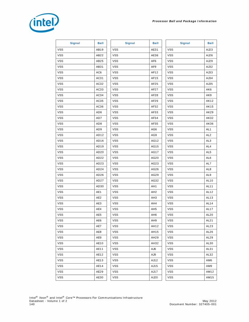
Intel® Xeon® and Intel® Core™ Processors For Communications InfrastructureDatasheet - Volume 1 of 2 May 2012140 Document Number: 327405-001
Processor Ball and Package Information
VSS AB19
VSS AB22
VSS AB25
VSS AB31
VSS AC6
VSS AC31
VSS AC32
VSS AC33
VSS AC34
VSS AC35
VSS AC36
VSS AD6
VSS AD7
VSS AD8
VSS AD9
VSS AD12
VSS AD16
VSS AD19
VSS AD20
VSS AD22
VSS AD23
VSS AD24
VSS AD26
VSS AD27
VSS AD30
VSS AE1
VSS AE2
VSS AE3
VSS AE4
VSS AE5
VSS AE6
VSS AE7
VSS AE8
VSS AE9
VSS AE10
VSS AE11
VSS AE12
VSS AE13
VSS AE14
VSS AE29
VSS AE30
Signal Ball
VSS AE31
VSS AE36
VSS AF6
VSS AF9
VSS AF12
VSS AF15
VSS AF25
VSS AF27
VSS AF28
VSS AF29
VSS AF32
VSS AF33
VSS AF34
VSS AF35
VSS AG6
VSS AG9
VSS AG12
VSS AG15
VSS AG17
VSS AG20
VSS AG23
VSS AG26
VSS AG29
VSS AG32
VSS AH1
VSS AH2
VSS AH3
VSS AH4
VSS AH5
VSS AH6
VSS AH9
VSS AH12
VSS AH15
VSS AH29
VSS AH32
VSS AJ6
VSS AJ9
VSS AJ12
VSS AJ15
VSS AJ17
VSS AJ20
Signal Ball
VSS AJ23
VSS AJ26
VSS AJ29
VSS AJ32
VSS AJ33
VSS AJ34
VSS AJ35
VSS AK6
VSS AK9
VSS AK12
VSS AK15
VSS AK29
VSS AK32
VSS AK36
VSS AL1
VSS AL2
VSS AL3
VSS AL4
VSS AL5
VSS AL6
VSS AL7
VSS AL8
VSS AL9
VSS AL10
VSS AL11
VSS AL12
VSS AL13
VSS AL14
VSS AL17
VSS AL20
VSS AL21
VSS AL23
VSS AL26
VSS AL29
VSS AL30
VSS AL31
VSS AL32
VSS AM6
VSS AM9
VSS AM12
VSS AM15
Signal Ball
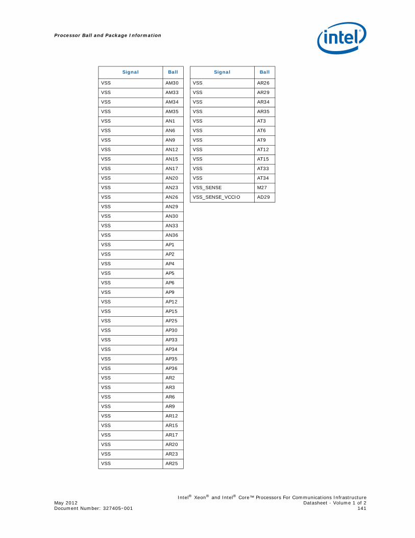
Intel® Xeon® and Intel® Core™ Processors For Communications InfrastructureMay 2012 Datasheet - Volume 1 of 2Document Number: 327405-001 141
Processor Ball and Package Information
VSS AM30
VSS AM33
VSS AM34
VSS AM35
VSS AN1
VSS AN6
VSS AN9
VSS AN12
VSS AN15
VSS AN17
VSS AN20
VSS AN23
VSS AN26
VSS AN29
VSS AN30
VSS AN33
VSS AN36
VSS AP1
VSS AP2
VSS AP4
VSS AP5
VSS AP6
VSS AP9
VSS AP12
VSS AP15
VSS AP25
VSS AP30
VSS AP33
VSS AP34
VSS AP35
VSS AP36
VSS AR2
VSS AR3
VSS AR6
VSS AR9
VSS AR12
VSS AR15
VSS AR17
VSS AR20
VSS AR23
VSS AR25
Signal Ball
VSS AR26
VSS AR29
VSS AR34
VSS AR35
VSS AT3
VSS AT6
VSS AT9
VSS AT12
VSS AT15
VSS AT33
VSS AT34
VSS_SENSE M27
VSS_SENSE_VCCIO AD29
Signal Ball
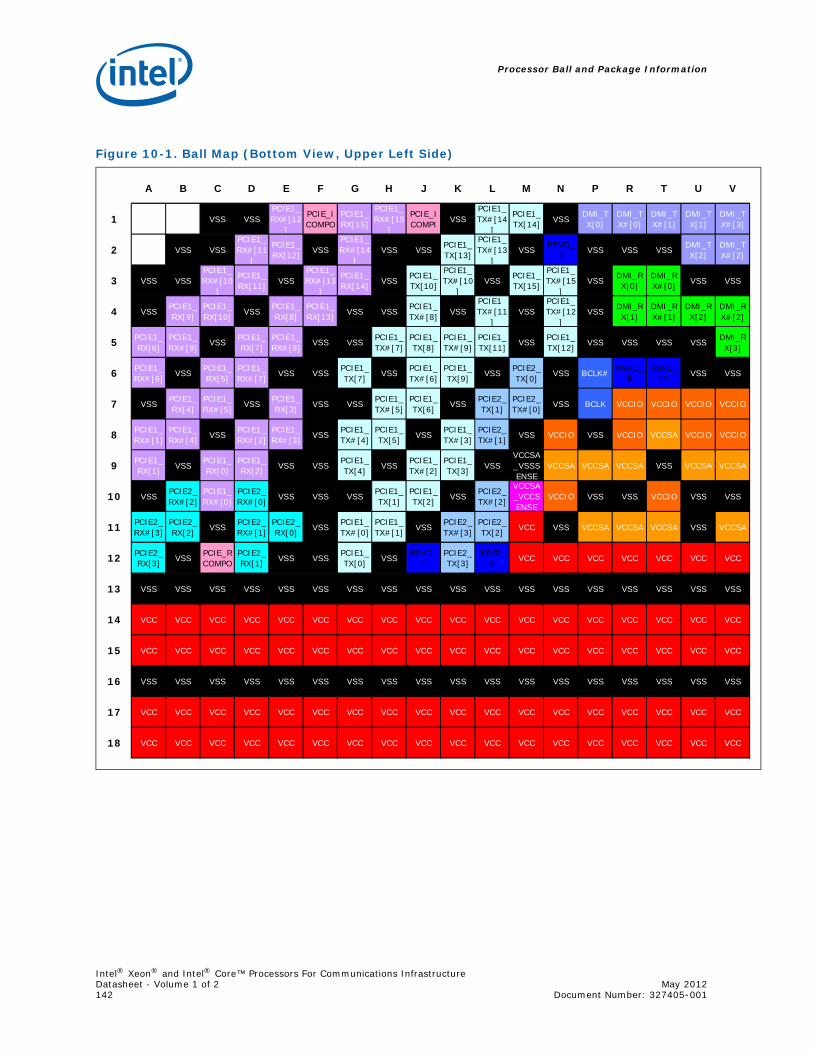
Processor Ball and Package Information
Intel® Xeon® and Intel® Core™ Processors For Communications InfrastructureDatasheet - Volume 1 of 2 May 2012142 Document Number: 327405-001
Figure 10-1. Ball Map (Bottom View, Upper Left Side)
A B C D E F G H J K L M N P R T U V
1 VSS VSSPCIE1_RX#[12
]
PCIE_ICOMPO
PCIE1_RX[15]
PCIE1_RX#[15
]
PCIE_ICOMPI VSS
PCIE1_TX#[14
]
PCIE1_TX[14] VSS DMI_T
X[0]DMI_TX#[0]
DMI_TX#[1]
DMI_TX[1]
DMI_TX#[3]
2 VSS VSSPCIE1_RX#[11
]
PCIE1_RX[12] VSS
PCIE1_RX#[14
]VSS VSS PCIE1_
TX[13]
PCIE1_TX#[13
]VSS RSVD_
6 VSS VSS VSS DMI_TX[2]
DMI_TX#[2]
3 VSS VSSPCIE1_RX#[10
]
PCIE1_RX[11] VSS
PCIE1_RX#[13
]
PCIE1_RX[14] VSS PCIE1_
TX[10]
PCIE1_TX#[10
]VSS PCIE1_
TX[15]
PCIE1_TX#[15
]VSS DMI_R
X[0]DMI_RX#[0] VSS VSS
4 VSS PCIE1_RX[9]
PCIE1_RX[10] VSS PCIE1_
RX[8]PCIE1_RX[13] VSS VSS PCIE1_
TX#[8] VSSPCIE1_TX#[11
]VSS
PCIE1_TX#[12
]VSS DMI_R
X[1]DMI_RX#[1]
DMI_RX[2]
DMI_RX#[2]
5 PCIE1_RX[6]
PCIE1_RX#[9] VSS PCIE1_
RX[7]PCIE1_RX#[8] VSS VSS PCIE1_
TX#[7]PCIE1_TX[8]
PCIE1_TX#[9]
PCIE1_TX[11] VSS PCIE1_
TX[12] VSS VSS VSS VSS DMI_RX[3]
6 PCIE1_RX#[6] VSS PCIE1_
RX[5]PCIE1_RX#[7] VSS VSS PCIE1_
TX[7] VSS PCIE1_TX#[6]
PCIE1_TX[9] VSS PCIE2_
TX[0] VSS BCLK# RSVD_9
RSVD_10 VSS VSS
7 VSS PCIE1_RX[4]
PCIE1_RX#[5] VSS PCIE1_
RX[3] VSS VSS PCIE1_TX#[5]
PCIE1_TX[6] VSS PCIE2_
TX[1]PCIE2_TX#[0] VSS BCLK VCCIO VCCIO VCCIO VCCIO
8 PCIE1_RX#[1]
PCIE1_RX#[4] VSS PCIE1_
RX#[2]PCIE1_RX#[3] VSS PCIE1_
TX#[4]PCIE1_TX[5] VSS PCIE1_
TX#[3]PCIE2_TX#[1] VSS VCCIO VSS VCCIO VCCSA VCCIO VCCIO
9 PCIE1_RX[1] VSS PCIE1_
RX[0]PCIE1_RX[2] VSS VSS PCIE1_
TX[4] VSS PCIE1_TX#[2]
PCIE1_TX[3] VSS
VCCSA_VSSSENSE
VCCSA VCCSA VCCSA VSS VCCSA VCCSA
10 VSS PCIE2_RX#[2]
PCIE1_RX#[0]
PCIE2_RX#[0] VSS VSS VSS PCIE1_
TX[1]PCIE1_TX[2] VSS PCIE2_
TX#[2]
VCCSA_VCCSENSE
VCCIO VSS VSS VCCIO VSS VSS
11 PCIE2_RX#[3]
PCIE2_RX[2] VSS PCIE2_
RX#[1]PCIE2_RX[0] VSS PCIE1_
TX#[0]PCIE1_TX#[1] VSS PCIE2_
TX#[3]PCIE2_TX[2] VCC VSS VCCSA VCCSA VCCSA VSS VCCSA
12 PCIE2_RX[3] VSS PCIE_R
COMPOPCIE2_RX[1] VSS VSS PCIE1_
TX[0] VSS RSVD_7
PCIE2_TX[3]
RSVD_8 VCC VCC VCC VCC VCC VCC VCC
13 VSS VSS VSS VSS VSS VSS VSS VSS VSS VSS VSS VSS VSS VSS VSS VSS VSS VSS
14 VCC VCC VCC VCC VCC VCC VCC VCC VCC VCC VCC VCC VCC VCC VCC VCC VCC VCC
15 VCC VCC VCC VCC VCC VCC VCC VCC VCC VCC VCC VCC VCC VCC VCC VCC VCC VCC
16 VSS VSS VSS VSS VSS VSS VSS VSS VSS VSS VSS VSS VSS VSS VSS VSS VSS VSS
17 VCC VCC VCC VCC VCC VCC VCC VCC VCC VCC VCC VCC VCC VCC VCC VCC VCC VCC
18 VCC VCC VCC VCC VCC VCC VCC VCC VCC VCC VCC VCC VCC VCC VCC VCC VCC VCC
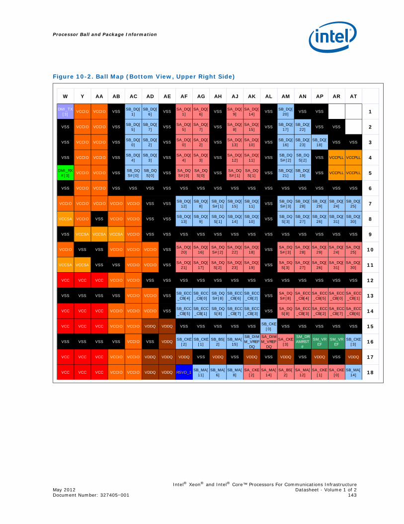
Processor Ball and Package Information
Intel® Xeon® and Intel® Core™ Processors For Communications InfrastructureMay 2012 Datasheet - Volume 1 of 2Document Number: 327405-001 143
Figure 10-2. Ball Map (Bottom View, Upper Right Side)
W Y AA AB AC AD AE AF AG AH AJ AK AL AM AN AP AR AT
DMI_TX[3]
VCCIO VCCIO VSS SB_DQ[1]
SB_DQ[6]
VSS SA_DQ[1]
SA_DQ[6]
VSS SA_DQ[9]
SA_DQ[14]
VSS SB_DQ[20]
VSS VSS 1
VSS VCCIO VCCIO VSS SB_DQ[5]
SB_DQ[7]
VSS SA_DQ[5]
SA_DQ[7]
VSS SA_DQ[8]
SA_DQ[15]
VSS SB_DQ[17]
SB_DQ[22]
VSS VSS 2
VSS VCCIO VCCIO VSS SB_DQ[0]
SB_DQ[2]
VSS SA_DQ[0]
SA_DQ[2]
VSS SA_DQ[13]
SA_DQ[10]
VSS SB_DQ[16]
SB_DQ[23]
SB_DQ[18]
VSS VSS 3
VSS VCCIO VCCIO VSS SB_DQ[4]
SB_DQ[3]
VSS SA_DQ[4]
SA_DQ[3]
VSS SA_DQ[12]
SA_DQ[11]
VSS SB_DQS#[2]
SB_DQS[2]
VSS VCCPLL VCCPLL 4
DMI_RX#[3]
VCCIO VCCIO VSS SB_DQS#[0]
SB_DQS[0]
VSS SA_DQS#[0]
SA_DQS[0]
VSS SA_DQS#[1]
SA_DQS[1]
VSS SB_DQ[21]
SB_DQ[19]
VSS VCCPLL VCCPLL 5
VSS VCCIO VCCIO VSS VSS VSS VSS VSS VSS VSS VSS VSS VSS VSS VSS VSS VSS VSS 6
VCCIO VCCIO VCCIO VCCIO VCCIO VSS VSS SB_DQ[12]
SB_DQ[8]
SB_DQS#[1]
SB_DQ[15]
SB_DQ[11]
VSS SB_DQS#[3]
SB_DQ[28]
SB_DQ[29]
SB_DQ[24]
SB_DQ[25] 7
VCCSA VCCIO VSS VCCIO VCCIO VSS VSS SB_DQ[13]
SB_DQ[9]
SB_DQS[1]
SB_DQ[14]
SB_DQ[10]
VSS SB_DQS[3]
SB_DQ[27]
SB_DQ[26]
SB_DQ[31]
SB_DQ[30] 8
VSS VCCSA VCCSA VCCSA VCCIO VSS VSS VSS VSS VSS VSS VSS VSS VSS VSS VSS VSS VSS 9
VCCIO VSS VSS VCCIO VCCIO VCCIO VSS SA_DQ[20]
SA_DQ[16]
SA_DQS#[2]
SA_DQ[22]
SA_DQ[18]
VSS SA_DQS#[3]
SA_DQ[28]
SA_DQ[29]
SA_DQ[24]
SA_DQ[25] 10
VCCSA VCCSA VSS VSS VCCIO VCCIO VSS SA_DQ[21]
SA_DQ[17]
SA_DQS[2]
SA_DQ[23]
SA_DQ[19]
VSS SA_DQS[3]
SA_DQ[27]
SA_DQ[26]
SA_DQ[31]
SA_DQ[30] 11
VCC VCC VCC VCCIO VCCIO VSS VSS VSS VSS VSS VSS VSS VSS VSS VSS VSS VSS VSS 12
VSS VSS VSS VSS VCCIO VCCIO VSS SB_ECC_CB[4]
SB_ECC_CB[0]
SB_DQS#[8]
SB_ECC_CB[6]
SB_ECC_CB[2]
VSS SA_DQS#[8]
SA_ECC_CB[4]
SA_ECC_CB[5]
SA_ECC_CB[0]
SA_ECC_CB[1] 13
VCC VCC VCC VCCIO VCCIO VCCIO VSS SB_ECC_CB[5]
SB_ECC_CB[1]
SB_DQS[8]
SB_ECC_CB[7]
SB_ECC_CB[3]
VSS SA_DQS[8]
SA_ECC_CB[3]
SA_ECC_CB[2]
SA_ECC_CB[7]
SA_ECC_CB[6] 14
VCC VCC VCC VCCIO VCCIO VDDQ VDDQ VSS VSS VSS VSS VSS SB_CKE[0]
VSS VSS VSS VSS VSS 15
VSS VSS VSS VSS VCCIO VSS VDDQ SB_CKE[2]
SB_CKE[1]
SB_BS[2]
SB_MA[15]
SB_DIMM_VREF
DQ
SA_DIMM_VREF
DQ
SA_CKE[3]
SM_DRAMRST
#
SM_VREF
SM_VREF
SB_CKE[3] 16
VCC VCC VCC VCCIO VCCIO VDDQ VDDQ VDDQ VSS VDDQ VSS VDDQ VSS VDDQ VSS VDDQ VSS VDDQ 17
VCC VCC VCC VCCIO VCCIO VDDQ VDDQ RSVD_1 SB_MA[11]
SB_MA[6]
SB_MA[8]
SA_CKE[2]
SA_MA[14]
SA_BS[2]
SA_MA[12]
SA_CKE[1]
SA_CKE[0]
SB_MA[14] 18
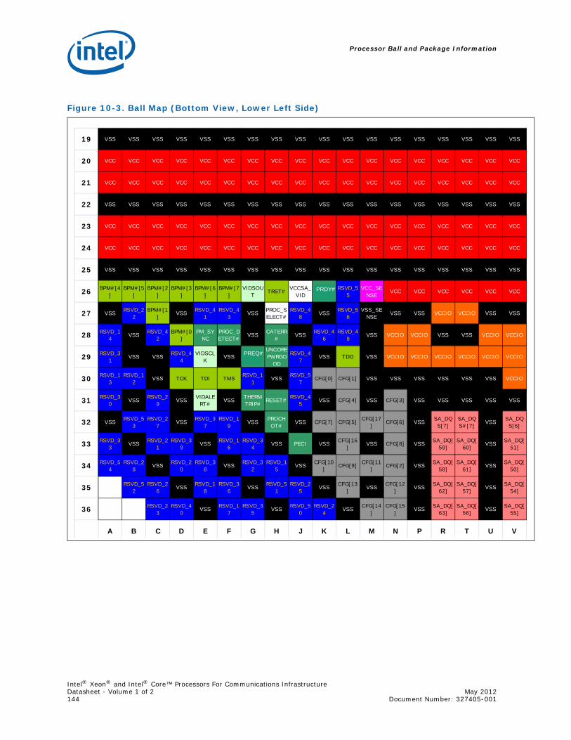
Processor Ball and Package Information
Intel® Xeon® and Intel® Core™ Processors For Communications InfrastructureDatasheet - Volume 1 of 2 May 2012144 Document Number: 327405-001
Figure 10-3. Ball Map (Bottom View, Lower Left Side)
19 VSS VSS VSS VSS VSS VSS VSS VSS VSS VSS VSS VSS VSS VSS VSS VSS VSS VSS
20 VCC VCC VCC VCC VCC VCC VCC VCC VCC VCC VCC VCC VCC VCC VCC VCC VCC VCC
21 VCC VCC VCC VCC VCC VCC VCC VCC VCC VCC VCC VCC VCC VCC VCC VCC VCC VCC
22 VSS VSS VSS VSS VSS VSS VSS VSS VSS VSS VSS VSS VSS VSS VSS VSS VSS VSS
23 VCC VCC VCC VCC VCC VCC VCC VCC VCC VCC VCC VCC VCC VCC VCC VCC VCC VCC
24 VCC VCC VCC VCC VCC VCC VCC VCC VCC VCC VCC VCC VCC VCC VCC VCC VCC VCC
25 VSS VSS VSS VSS VSS VSS VSS VSS VSS VSS VSS VSS VSS VSS VSS VSS VSS VSS
26 BPM#[4]
BPM#[5]
BPM#[2]
BPM#[3]
BPM#[6]
BPM#[7]
VIDSOUT
TRST# VCCSA_VID
PRDY RSVD_55
VCC_SENSE
VCC VCC VCC VCC VCC VCC
27 VSS RSVD_22
BPM#[1]
VSS RSVD_41
RSVD_43
VSS PROC_SELECT#
RSVD_48
VSS RSVD_56
VSS_SENSE
VSS VSS VCCIO VCCIO VSS VSS
28 RSVD_14
VSS RSVD_42
BPM#[0]
PM_SYNC
PROC_DETECT#
VSS CATERR#
VSS RSVD_46
RSVD_49
VSS VCCIO VCCIO VSS VSS VCCIO VCCIO
29 RSVD_31
VSS VSS RSVD_44
VIDSCLK
VSS PREQUNCOREPWRGO
OD
RSVD_47
VSS TDO VSS VCCIO VCCIO VCCIO VCCIO VCCIO VCCIO
30 RSVD_13
RSVD_12
VSS TCK TDI TMS RSVD_11
VSS RSVD_57
CFG[0] CFG[1] VSS VSS VSS VSS VSS VSS VCCIO
31 RSVD_30
VSS RSVD_29
VSS VIDALERT#
VSS THERMTRIP#
RESET# RSVD_45
VSS CFG[4] VSS CFG[3] VSS VSS VSS VSS VSS
32 VSS RSVD_53
RSVD_27
VSS RSVD_37
RSVD_19
VSS PROCHOT#
VSS CFG[7] CFG[5] CFG[17]
CFG[6] VSS SA_DQS[7]
SA_DQS#[7]
VSS SA_DQS[6]
33 RSVD_33
VSS RSVD_21
RSVD_39
VSS RSVD_16
RSVD_34
VSS PECI VSS CFG[16]
VSS CFG[8] VSS SA_DQ[59]
SA_DQ[60]
VSS SA_DQ[51]
34 RSVD_54
RSVD_28
VSS RSVD_20
RSVD_38
VSS RSVD_32
RSVD_15
VSS CFG[10]
CFG[9] CFG[11]
CFG[2] VSS SA_DQ[58]
SA_DQ[61]
VSS SA_DQ[50]
35 RSVD_52
RSVD_26
VSS RSVD_18
RSVD_36
VSS RSVD_51
RSVD_25
VSS CFG[13]
VSS CFG[12]
VSS SA_DQ[62]
SA_DQ[57]
VSS SA_DQ[54]
36 RSVD_23
RSVD_40
VSS RSVD_17
RSVD_35
VSS RSVD_50
RSVD_24
VSS CFG[14]
CFG[15]
VSS SA_DQ[63]
SA_DQ[56]
VSS SA_DQ[55]
A B C D E F G H J K L M N P R T U V
PRDY#
PREQ#
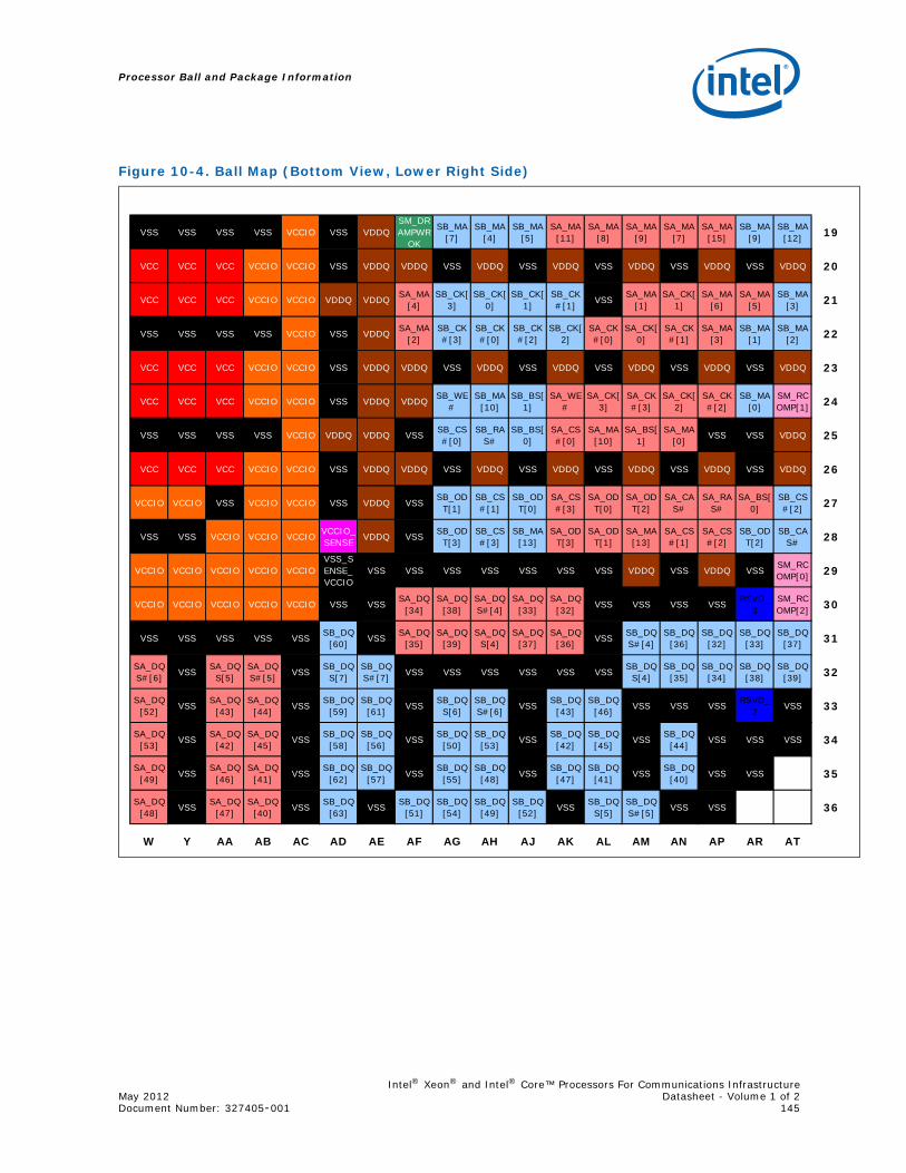
Processor Ball and Package Information
Intel® Xeon® and Intel® Core™ Processors For Communications InfrastructureMay 2012 Datasheet - Volume 1 of 2Document Number: 327405-001 145
Figure 10-4. Ball Map (Bottom View, Lower Right Side)
VSS VSS VSS VSS VCCIO VSS VDDQSM_DRAMPWR
OK
SB_MA[7]
SB_MA[4]
SB_MA[5]
SA_MA[11]
SA_MA[8]
SA_MA[9]
SA_MA[7]
SA_MA[15]
SB_MA[9]
SB_MA[12] 19
VCC VCC VCC VCCIO VCCIO VSS VDDQ VDDQ VSS VDDQ VSS VDDQ VSS VDDQ VSS VDDQ VSS VDDQ 20
VCC VCC VCC VCCIO VCCIO VDDQ VDDQ SA_MA[4]
SB_CK[3]
SB_CK[0]
SB_CK[1]
SB_CK#[1] VSS SA_MA
[1]SA_CK[
1]SA_MA
[6]SA_MA
[5]SB_MA
[3] 21
VSS VSS VSS VSS VCCIO VSS VDDQ SA_MA[2]
SB_CK#[3]
SB_CK#[0]
SB_CK#[2]
SB_CK[2]
SA_CK#[0]
SA_CK[0]
SA_CK#[1]
SA_MA[3]
SB_MA[1]
SB_MA[2] 22
VCC VCC VCC VCCIO VCCIO VSS VDDQ VDDQ VSS VDDQ VSS VDDQ VSS VDDQ VSS VDDQ VSS VDDQ 23
VCC VCC VCC VCCIO VCCIO VSS VDDQ VDDQ SB_WE#
SB_MA[10]
SB_BS[1]
SA_WE#
SA_CK[3]
SA_CK#[3]
SA_CK[2]
SA_CK#[2]
SB_MA[0]
SM_RCOMP[1] 24
VSS VSS VSS VSS VCCIO VDDQ VDDQ VSS SB_CS#[0]
SB_RAS#
SB_BS[0]
SA_CS#[0]
SA_MA[10]
SA_BS[1]
SA_MA[0] VSS VSS VDDQ 25
VCC VCC VCC VCCIO VCCIO VSS VDDQ VDDQ VSS VDDQ VSS VDDQ VSS VDDQ VSS VDDQ VSS VDDQ 26
VCCIO VCCIO VSS VCCIO VCCIO VSS VDDQ VSS SB_ODT[1]
SB_CS#[1]
SB_ODT[0]
SA_CS#[3]
SA_ODT[0]
SA_ODT[2]
SA_CAS#
SA_RAS#
SA_BS[0]
SB_CS#[2] 27
VSS VSS VCCIO VCCIO VCCIO VCCIO_SENSE VDDQ VSS SB_OD
T[3]SB_CS#[3]
SB_MA[13]
SA_ODT[3]
SA_ODT[1]
SA_MA[13]
SA_CS#[1]
SA_CS#[2]
SB_ODT[2]
SB_CAS# 28
VCCIO VCCIO VCCIO VCCIO VCCIOVSS_SENSE_VCCIO
VSS VSS VSS VSS VSS VSS VSS VDDQ VSS VDDQ VSS SM_RCOMP[0] 29
VCCIO VCCIO VCCIO VCCIO VCCIO VSS VSS SA_DQ[34]
SA_DQ[38]
SA_DQS#[4]
SA_DQ[33]
SA_DQ[32] VSS VSS VSS VSS RSVD_
3SM_RCOMP[2] 30
VSS VSS VSS VSS VSS SB_DQ[60] VSS SA_DQ
[35]SA_DQ[39]
SA_DQS[4]
SA_DQ[37]
SA_DQ[36] VSS SB_DQ
S#[4]SB_DQ[36]
SB_DQ[32]
SB_DQ[33]
SB_DQ[37] 31
SA_DQS#[6] VSS SA_DQ
S[5]SA_DQS#[5] VSS SB_DQ
S[7]SB_DQS#[7] VSS VSS VSS VSS VSS VSS SB_DQ
S[4]SB_DQ[35]
SB_DQ[34]
SB_DQ[38]
SB_DQ[39] 32
SA_DQ[52] VSS SA_DQ
[43]SA_DQ[44] VSS SB_DQ
[59]SB_DQ[61] VSS SB_DQ
S[6]SB_DQS#[6] VSS SB_DQ
[43]SB_DQ[46] VSS VSS VSS RSVD_
2 VSS 33
SA_DQ[53] VSS SA_DQ
[42]SA_DQ[45] VSS SB_DQ
[58]SB_DQ[56] VSS SB_DQ
[50]SB_DQ[53] VSS SB_DQ
[42]SB_DQ[45] VSS SB_DQ
[44] VSS VSS VSS 34
SA_DQ[49] VSS SA_DQ
[46]SA_DQ[41] VSS SB_DQ
[62]SB_DQ[57] VSS SB_DQ
[55]SB_DQ[48] VSS SB_DQ
[47]SB_DQ[41] VSS SB_DQ
[40] VSS VSS 35
SA_DQ[48] VSS SA_DQ
[47]SA_DQ[40] VSS SB_DQ
[63] VSS SB_DQ[51]
SB_DQ[54]
SB_DQ[49]
SB_DQ[52] VSS SB_DQ
S[5]SB_DQS#[5] VSS VSS 36
W Y AA AB AC AD AE AF AG AH AJ AK AL AM AN AP AR AT
Processor Ball and Package Information
Intel® Xeon® and Intel® Core™ Processors For Communications InfrastructureDatasheet - Volume 1 of 2 May 2012146 Document Number: 327405-001
10.2 Package Mechanical InformationThe following section contains the mechanical drawings for the processor. The processor utilizes a 37.5 x 37.5 mm, FC-BGA package. There are two versions of die available on this package — a 4-Core-die version and a 2-Core-die version. The processor SKUs and their corresponding die-type are provided in Table 5-1, “Base Features by SKU” on page 45.
The primary mechanical difference between the two products is the size of the die on the substrate. The pinout, package substrate and solder ball pattern are the same between the two packages.
See the following package drawings for the die size of the two processor packages. Figure 10-5 shows the 4-Core Die Mechanical Package and Figure 10-6 shows the 2-Core Die / 1-Core Die Mechanical Package. The dimensions in the figures are in millimeters.
Remember to check the size differences between the two dies when designing your thermal solution.
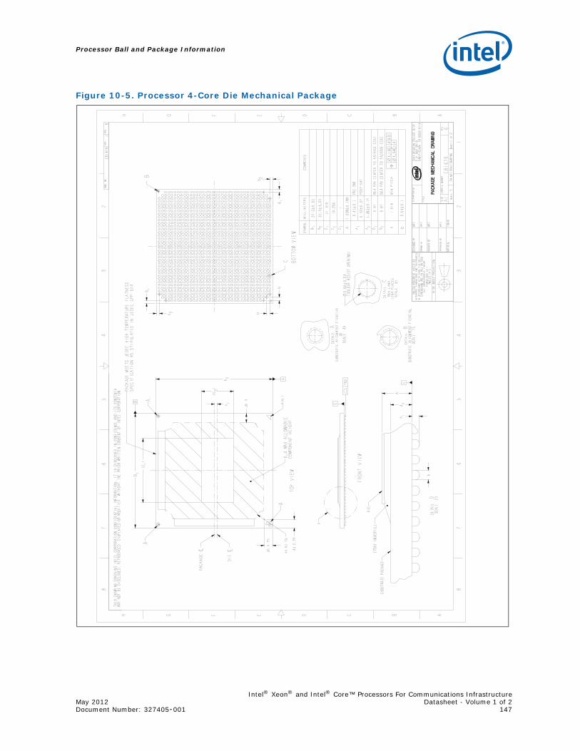
Processor Ball and Package Information
Intel® Xeon® and Intel® Core™ Processors For Communications InfrastructureMay 2012 Datasheet - Volume 1 of 2Document Number: 327405-001 147
Figure 10-5. Processor 4-Core Die Mechanical Package
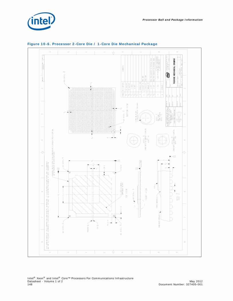
Processor Ball and Package Information
Intel® Xeon® and Intel® Core™ Processors For Communications InfrastructureDatasheet - Volume 1 of 2 May 2012148 Document Number: 327405-001
Figure 10-6. Processor 2-Core Die / 1-Core Die Mechanical Package
Processor Ball and Package Information
Intel® Xeon® and Intel® Core™ Processors For Communications InfrastructureMay 2012 Datasheet - Volume 1 of 2Document Number: 327405-001 149
§ §
Processor Ball and Package Information
Intel® Xeon® and Intel® Core™ Processors For Communications InfrastructureDatasheet - Volume 1 of 2 May 2012150 Document Number: 327405-001
Processor Configuration Registers
Intel® Xeon® and Intel® Core™ Processors For Communications InfrastructureMay 2012 Datasheet - Volume 1 of 2Document Number: 327405-001 151
11.0 Processor Configuration Registers
This section contains register information that is specific to the Intel® Xeon®, Intel® Core™, Intel® Pentium® and Intel® Celeron® Processors for Communications Infrastructure. For other register details see the latest version of the 2nd Generation Intel® Core™ Processor Family Mobile Datasheet – Volume 2.
Note: The processor does not include the Integrated Display Engine or the Graphics Processor Unit (GPU). Disregard references to graphics and Intel® Turbo Boost in the 2nd Generation Intel® Core™ Processor Family Mobile Datasheet – Volume 2.
Table 11-1 shows the register-related terminology that is used in this document.
Table 11-2 lists the modifiers used in conjunction with attributes that are included in the register tables throughout this document.
Table 11-1. Register Terminology
Item Description
RO Read Only: These bits can only be read by software, writes have no effect. The value of the bits is determined by the hardware only.
RW Read/Write: These bits can be read and written by software.
RW1C Read / Write 1 to Clear: These bits can be read and cleared by software. Writing a '1' to a bit will clear it, while writing a '0' to a bit has no effect. Hardware sets these bits.
RW0C Read/Write 0 to Clear: These bits can be read and cleared by software. Writing a ‘0’ to a bit will clear it, while writing a ‘1’ to a bit has no effect. Hardware sets these bits.
RW1S Read / Write 1 to Set: These bits can be read and set by software. Writing a ‘1’ to a bit will set it, while writing a ‘0’ to a bit has no effect. Hardware clears these bits.
RsvdP
Reserved and Preserved: These bits are reserved for future RW implementations and their value must not be modified by software. When writing to these bits, software must preserve the value read. When SW updates a register that has RsvdP fields, it must read the register value first so that the appropriate merge between the RsvdP and updated fields will occur.
RsvdZ Reserved and Zero: These bits are reserved for future RW1C implementations. SW must use 0 for writes.
WOWrite Only: These bits can only be written by software, reads return zero. NOTE: Use of this attribute type is deprecated and can only be used to describe bits without persistent state.
RC
Read Clear: These bits can only be read by software, but a read causes the bits to be cleared. Hardware sets these bits. NOTE: Use of this attribute type is only allowed on legacy functions, as side-effects on reads are not desirable
RSW1C Read Set / Write 1 to Clear: These bits can be read and cleared by software. Reading a bit will set the bit to ‘1’. Writing a ‘1’ to a bit will clear it, while writing a ‘0’ to a bit has no effect.
RCW
Read Clear / Write: These bits can be read and written by software, but a read causes the bits to be cleared. NOTE: Use of this attribute type is only allowed on legacy functions, as side-effects on reads are not desirable.
Processor Configuration Registers
Intel® Xeon® and Intel® Core™ Processors For Communications InfrastructureDatasheet - Volume 1 of 2 May 2012152 Document Number: 327405-001
11.1 ERRSTS - Error StatusB/D/F/Type: 0/0/0/PCI
Address Offset: C8-C9h
Default Value: 0000h
Access: RO; RW1C-S
Size: 16 bits
BIOS Optimal Default 0000h
This register is used to report various error conditions via the SERR DMI messaging mechanism. The SERR DMI message is generated on a zero to one transition of any of these flags (if enabled by the ERRCMD and PCICMD registers).
These bits are set regardless of whether or not the SERR is enabled and generated. After the error processing is complete, the error logging mechanism can be unlocked by clearing the appropriate status bit by software writing a '1' to it.
Table 11-2. Register Terminology Attribute Modifier
Attribute Modifier Applicable Attribute Description
S
RO (with -V)
Sticky: These bits are only re-initialized to their default value by a Power Good Reset. Note: Does not apply to RO (constant) bits.
RW
RW1C
RW1S
-K RW Key: These bits control the ability to write other bits (identified with a Lock modifier).
-LRW Lock: Hardware can make these bits Read-Only via a
separate configuration bit or other logic. Note: Mutually exclusive with Once modifier.WO
-ORW Once: After reset, these bits can only be rewritten by
software once after which they become Read Only. Note: Mutually exclusive with Variant modifierWO
-FW RO Firmware Write: The value of these bits can be updated by firmware (PCU, TAR, etc.).
-V RO
Variant: The value of these bits can be updated by hardware. Note: RW1C and RC are variant by definition and therefore do not need to be modified.
Table 11-3. Error Status Register (Sheet 1 of 2)
Bit Access Default Value
RST/PWR Description
15:2 RO 0h Reserved (RSVD)
Processor Configuration Registers
Intel® Xeon® and Intel® Core™ Processors For Communications InfrastructureMay 2012 Datasheet - Volume 1 of 2Document Number: 327405-001 153
11.2 ERRCMD - Error CommandB/D/F/Type: 0/0/0/PCI
Address Offset: CA-CBh
Default Value: 0000h
Access: RO; RW
Size: 16 bits
BIOS Optimal Default 0000h
This register controls the Host Bridge responses to various system errors. Since the Host Bridge does not have an SERRB signal, SERR messages are passed from the Processor to the PCH over DMI.
When a bit in this register is set, a SERR message will be generated on DMI whenever the corresponding flag is set in the ERRSTS register. The actual generation of the SERR message is globally enabled for Device 0 via the PCI Command register.
1 RW1C-S 0b Powergood
Multiple-bit DRAM ECC Error Flag (DMERR): If this bit is set to 1, a memory read data transfer had an uncorrectable multiple-bit error. When this bit is set, the column, row, bank, and rank that caused the error, and the error syndrome, are logged in the ECC Error Log register in the channel where the error occurred. Once this bit is set, the ECCERRLOGx fields are locked until the processor clears this bit by writing a 1. Software uses bits [1:0] to detect whether the logged error address is for a Single-bit or a Multiple-bit error. This bit is reset on PWROK.
0 RW1C-S 0b Powergood
Single-bit DRAM ECC Error Flag (DSERR): If this bit is set to 1, a memory read data transfer had a single-bit correctable error and the corrected data was returned to the requesting agent. When this bit is set the column, row, bank, and rank where the error occurred and the syndrome of the error are logged in the ECC Error Log register in the channel where the error occurred. Once this bit is set the ECCERRLOGx fields are locked to further single-bit error updates until the CPU clears this bit by writing a 1. A multiple bit error that occurs after this bit is set will overwrite the ECCERRLOGx fields with the multiple-bit error signature and the DMERR bit will also be set. A single bit error that occurs after a multibit error will set this bit but will not overwrite the other fields. This bit is reset on PWROK.
Table 11-3. Error Status Register (Sheet 2 of 2)
Bit Access Default Value
RST/PWR Description
Processor Configuration Registers
Intel® Xeon® and Intel® Core™ Processors For Communications InfrastructureDatasheet - Volume 1 of 2 May 2012154 Document Number: 327405-001
11.3 SMICMD - SMI Command B/D/F/Type: 0/0/0/PCI
Address Offset: CC-CDh
Default Value: 0000h
Access: RO; RW
Size: 16 bits
BIOS Optimal Default 0000h
This register enables various errors to generate an SMI DMI special cycle. When an error flag is set in the ERRSTS register, it can generate an SERR, SMI, or SCI DMI special cycle when enabled in the ERRCMD, SMICMD, or SCICMD registers respectively. One and only one message type can be enabled.
Table 11-4. Error Command Registers
Bit Access Default Value
RST/PWR Description
15:2 RO 0h Reserved (RSVD)
1 RW 0b Uncore
SERR Multiple-Bit DRAM ECC Error (DMERR):1 = The Host Bridge generates an SERR message
over DMI when it detects a multiple-bit error reported by the DRAM controller.
0 = Reporting of this condition via SERR messaging is disabled.
For systems not supporting ECC, this bit must be disabled.
0 RW 0b Uncore
SERR on Single-bit ECC Error (DSERR):1 = The Host Bridge generates an SERR special cycle
over DMI when the DRAM controller detects a single bit error.
0 = Reporting of this condition via SERR messaging is disabled.
For systems that do not support ECC, this bit must be disabled.
Table 11-5. SMI Command Registers
Bit Access Default Value
RST/PWR Description
15:2 RO 0h Reserved (RSVD)
1 RW 0b Uncore
SMI on Multiple-Bit DRAM ECC Error (DMESMI):1 = The Host generates an SMI DMI message when it
detects a multiple-bit error reported by the DRAM controller.
0 = Reporting of this condition via SMI messaging is disabled. For systems not supporting ECC, this bit must be disabled.
0 RW 0b Uncore
SMI on Single-bit ECC Error (DSESMI):1 = The Host generates an SMI DMI special cycle
when the DRAM controller detects a single bit error.
0 = Reporting of this condition via SMI messaging is disabled. For systems that do not support ECC, this bit must be disabled.
Processor Configuration Registers
Intel® Xeon® and Intel® Core™ Processors For Communications InfrastructureMay 2012 Datasheet - Volume 1 of 2Document Number: 327405-001 155
11.4 SCICMD - SCI CommandB/D/F/Type: 0/0/0/PCI
Address Offset: CE-CFh
Default Value: 0000h
Access: RO; RW
Size: 16 bits
BIOS Optimal Default 0000h
This register enables various errors to generate an SCI DMI special cycle. When an error flag is set in the ERRSTS register, it can generate an SERR, SMI, or SCI DMI special cycle when enabled in the ERRCMD, SMICMD, or SCICMD registers respectively. One and only one message type can be enabled.
11.5 ECCERRLOG0_C0 - ECC Error Log 0B/D/F/Type: 0/0/0/MCHBAR MC0
Address Offset: 40C8-40CBh
Default Value: 00000000h
Access: ROS-V
Size: 32 bits
BIOS Optimal Default 0000h
This Channel 0 register is used to store the error status information in ECC enabled configurations, along with the error syndrome and the rank and bank address information of the address block of main memory of which an error (single bit or multi-bit error) has occurred. The address fields represent the address of the first single or the first multiple bit error occurrence after the error flag bits in the ERRSTS register have been cleared by software. A multiple bit error will overwrite a single bit error.
Table 11-6. SCI Command Registers
Bit Access Default Value
RST/PWR Description
15:2 RO 0h Reserved (RSVD)
1 RW 0b Uncore
SCI on Multiple-Bit DRAM ECC Error (DMESMI):1 = The Host generates an SCI DMI message when it
detects a multiple-bit error reported by the DRAM controller.
0 = Reporting of this condition via SCI messaging is disabled. For systems not supporting ECC, this bit must be disabled.
0 RW 0b Uncore
SCI on Single-bit ECC Error (DSESMI):1 = The Host generates an SCI DMI special cycle
when the DRAM controller detects a single bit error.
0 = Reporting of this condition via SCI messaging is disabled. For systems that do not support ECC, this bit must be disabled.
Processor Configuration Registers
Intel® Xeon® and Intel® Core™ Processors For Communications InfrastructureDatasheet - Volume 1 of 2 May 2012156 Document Number: 327405-001
Once the error flag bits are set as a result of an error, this bit field is locked and doesn't change as a result of a new error until the error flag is cleared by software. Same is the case with error syndrome field.
11.6 ECCERRLOG1_C0 - ECC Error Log 1B/D/F/Type: 0/0/0/MCHBAR MC0
Address Offset: 40CC-40CFh
Default Value: 00000000h
Access: ROS-V
Size: 32 bits
This register is used to store the error status information in ECC enabled configurations, along with the error syndrome and the row and column address information of the address block of main memory of which an error (single bit or multi-bit error) has occurred.
Table 11-7. Channel 0 ECC Error Log 0
Bit Access Default Value
RST/PWR Description
31:29 ROS-V 000b PowergoodError Bank Address (ERRBANK):This field holds the Bank Address of the read transaction that had the ECC error.
28:27 ROS-V 00b PowergoodError Rank Address (ERRRANK):This field holds the Rank ID of the read transaction that had the ECC error.
26:24 ROS-V 000b PowergoodError Chunk (ERRCHUNK):Holds the chunk number of the error stored in the register.
23:16 ROS-V 00h Powergood
Error Syndrome (ERRSYND):This field contains the error syndrome. A value of FFh indicates that the error is due to poisoning.Note: For ERRSYND definition see Table 11-13,
“Error Syndrome - ERRSYND”
15:2 RO 0h Reserved (RSVD)
1 ROS-V 0b Powergood
Multiple Bit Error Status (MERRSTS):This bit is set when an uncorrectable multiple-bit error occurs on a memory read data transfer. When this bit is set, the address that caused the error and the error syndrome are also logged and they are locked until this bit is cleared.This bit is cleared when the corresponding bit in0.0.0.PCI.ERRSTS is cleared.
0 ROS-V 0b Powergood
Correctable Error Status (CERRSTS):This bit is set when a correctable single-bit error occurs on a memory read data transfer. When this bit is set, the address that caused the error and the error syndrome are also logged and they are locked to further single bit errors, until this bit is cleared.A multiple bit error that occurs after this bit is set will override the address/error syndrome information.This bit is cleared when the corresponding bit in 0.0.0.PCI.ERRSTS is cleared.
Processor Configuration Registers
Intel® Xeon® and Intel® Core™ Processors For Communications InfrastructureMay 2012 Datasheet - Volume 1 of 2Document Number: 327405-001 157
11.7 ECCERRLOG0_C1 - ECC Error Log 0B/D/F/Type: 0/0/0/MCHBAR MC1
Address Offset: 44C8-44CBh
Default Value: 00000000h
Access: ROS-V
Size: 32 bits
BIOS Optimal Default 0000h
This Channel 1 register is used to store the error status information in ECC enabled configurations, along with the error syndrome and the rank and bank address information of the address block of main memory of which an error (single bit or multi-bit error) has occurred. The address fields represent the address of the first single or the first multiple bit error occurrence after the error flag bits in the ERRSTS register have been cleared by software. A multiple bit error will overwrite a single bit error. Once the error flag bits are set as a result of an error, this bit field is locked and doesn't change as a result of a new error until the error flag is cleared by software. Same is the case with error syndrome field.
Table 11-8. Channel 0 ECC Error Log 1
Bit Access Default Value
RST/PWR Description
31:16 ROS-V 0000h PowergoodError Column (ERRCOL):This field holds the DRAM column address of the read transaction that had the ECC error.
15:0 ROS-V 0000h PowergoodError Row (ERRROW):This field holds the DRAM row (page) address of the read transaction that had the ECC error.
Table 11-9. Channel 1 ECC Error Log 0 (Sheet 1 of 2)
Bit Access Default Value
RST/PWR Description
31:29 ROS-V 000b PowergoodError Bank Address (ERRBANK):This field holds the Bank Address of the read transaction that had the ECC error.
28:27 ROS-V 00b PowergoodError Rank Address (ERRRANK):This field holds the Rank ID of the read transaction that had the ECC error.
26:24 ROS-V 000b PowergoodError Chunk (ERRCHUNK):Holds the chunk number of the error stored in the register.
23:16 ROS-V 00h Powergood
Error Syndrome (ERRSYND):This field contains the error syndrome. A value of FFh indicates that the error is due to poisoning.For ERRSYND definition see Table 11-13, “Error Syndrome - ERRSYND”
15:2 RO 0h Reserved (RSVD)
Processor Configuration Registers
Intel® Xeon® and Intel® Core™ Processors For Communications InfrastructureDatasheet - Volume 1 of 2 May 2012158 Document Number: 327405-001
11.8 ECCERRLOG1_C1 - ECC Error Log 1B/D/F/Type: 0/0/0/MCHBAR MC1
Address Offset: 44CC-44CFh
Default Value: 00000000h
Access: ROS-V
Size: 32 bits
This register is used to store the error status information in ECC enabled configurations, along with the error syndrome and the row and column address information of the address block of main memory of which an error (single bit or multi-bit error) has occurred.
11.9 MAD_DIMM_CH0 - Address Decode Channel 0B/D/F/Type: 0/0/0/MCHBAR_MCMAIN
Address Offset: 5004-5007h
Default Value: 00600000h
Access: RW-L
1 RO-P 0b Powergood
Multiple Bit Error Status (MERRSTS):This bit is set when an uncorrectable multiple-bit error occurs on a memory read data transfer. When this bit is set, the address that caused the error and the error syndrome are also logged and they are locked until this bit is cleared.This bit is cleared when the corresponding bit in0.0.0.PCI.ERRSTS is cleared.
0 RO-P 0b Powergood
Correctable Error Status (CERRSTS):This bit is set when a correctable single-bit error occurs on a memory read data transfer. When this bit is set, the address that caused the error and the error syndrome are also logged and they are locked to further single bit errors, until this bit is cleared.A multiple bit error that occurs after this bit is set will override the address/error syndrome information.This bit is cleared when the corresponding bit in 0.0.0.PCI.ERRSTS is cleared.
Table 11-9. Channel 1 ECC Error Log 0 (Sheet 2 of 2)
Bit Access Default Value
RST/PWR Description
Table 11-10.Channel 1 ECC Error Log 1
Bit Access Default Value
RST/PWR Description
31:16 ROS-V 0000h PowergoodError Column (ERRCOL):This field holds the DRAM column address of the read transaction that had the ECC error.
15:0 ROS-V 0000h PowergoodError Row (ERRROW):This field holds the DRAM row (page) address of the read transaction that had the ECC error.
Processor Configuration Registers
Intel® Xeon® and Intel® Core™ Processors For Communications InfrastructureMay 2012 Datasheet - Volume 1 of 2Document Number: 327405-001 159
Size: 32 bits
BIOS Optimal Default 00h
This register defines channel characteristics - number of DIMMs, number of ranks, size, ECC, interleave options and ECC options.
Table 11-11.Address Decode Channel 0
Bit Access Default Value
RST/PWR Description
31:26 RO 0h Reserved (RSVD)
25:24 RW-L 00b Uncore
ECC is active in the channel (ECC): 00 =no ECC active in the channel 01 =ECC is active in IO, ECC logic is not active In this
case, on write accesses the data driven on ECC byte is copied from DQ 7:0 (to be used in training or IOSAV)
10 =ECC is disabled in IO, but ECC logic is enabled (to be used in ECC4ANA mode)
11 =ECC active in both IO and ECC logic
23:23 RO 0h Reserved (RSVD)
22 RW-L 1b UncoreEnhanced Interleave mode (Enh_Interleave): 0 = off 1 = on
21 RW-L 1b Uncore
Rank Interleave (RI): Rank Interleave 0 = off 1 = on
20 RW-L 0b Uncore
DIMM B DDR width (DBW): DIMM B width of DDR chips 0 = X8 chips 1 = X16 chips
19 RW-L 0b Uncore
DIMM A DDR width (DAW): DIMM A width of DDR chips 0 = X8 chips 1 = X16 chips
18 RW-L 0b Uncore DIMM B number of ranks (DBNOR): 0 = single rank 1 = dual rank
17 RW-L 0b Uncore DIMM A number of ranks (DANOR):0 = single rank 1 = dual rank
16 RW-L 0b Uncore
DIMM A select (DAS): Selects which of the DIMMs is DIMM A - should be the larger DIMM:0 - DIMM 01 - DIMM 1
15:8 RW-L 00h Uncore Size of DIMM B (DIMM_B_Size):Size of DIMM B 256 MB multiples
7:0 RW-L 00h Uncore Size of DIMM A (DIMM_A_Size):Size of DIMM A 256 MB multiples
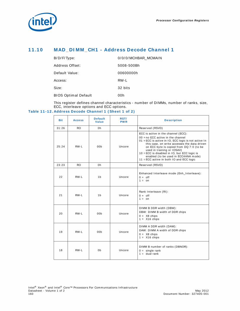
Processor Configuration Registers
Intel® Xeon® and Intel® Core™ Processors For Communications InfrastructureDatasheet - Volume 1 of 2 May 2012160 Document Number: 327405-001
11.10 MAD_DIMM_CH1 - Address Decode Channel 1B/D/F/Type: 0/0/0/MCHBAR_MCMAIN
Address Offset: 5008-500Bh
Default Value: 00600000h
Access: RW-L
Size: 32 bits
BIOS Optimal Default 00h
This register defines channel characteristics - number of DIMMs, number of ranks, size, ECC, interleave options and ECC options.
Table 11-12.Address Decode Channel 1 (Sheet 1 of 2)
Bit Access Default Value
RST/PWR Description
31:26 RO 0h Reserved (RSVD)
25:24 RW-L 00b Uncore
ECC is active in the channel (ECC): 00 =no ECC active in the channel 01 =ECC is active in IO, ECC logic is not active In
this case, on write accesses the data driven on ECC byte is copied from DQ 7:0 (to be used in training or IOSAV)
10 =ECC is disabled in IO, but ECC logic is enabled (to be used in ECC4ANA mode)
11 =ECC active in both IO and ECC logic
23:23 RO 0h Reserved (RSVD)
22 RW-L 1b UncoreEnhanced Interleave mode (Enh_Interleave): 0 = off 1 = on
21 RW-L 1b UncoreRank Interleave (RI): 0 = off 1 = on
20 RW-L 00b Uncore
DIMM B DDR width (DBW): DBW: DIMM B width of DDR chips 0 = X8 chips 1 = X16 chips
19 RW-L 00b Uncore
DIMM A DDR width (DAW): DAW: DIMM A width of DDR chips 0 = X8 chips 1 = X16 chips
18 RW-L 0b Uncore DIMM B number of ranks (DBNOR): 0 = single rank 1 = dual rank
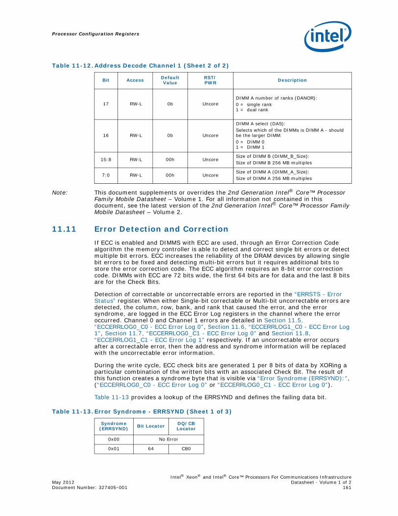
Processor Configuration Registers
Intel® Xeon® and Intel® Core™ Processors For Communications InfrastructureMay 2012 Datasheet - Volume 1 of 2Document Number: 327405-001 161
Note: This document supplements or overrides the 2nd Generation Intel® Core™ Processor Family Mobile Datasheet – Volume 1. For all information not contained in this document, see the latest version of the 2nd Generation Intel® Core™ Processor Family Mobile Datasheet – Volume 2.
11.11 Error Detection and CorrectionIf ECC is enabled and DIMMS with ECC are used, through an Error Correction Code algorithm the memory controller is able to detect and correct single bit errors or detect multiple bit errors. ECC increases the reliability of the DRAM devices by allowing single bit errors to be fixed and detecting multi-bit errors but it requires additional bits to store the error correction code. The ECC algorithm requires an 8-bit error correction code. DIMMs with ECC are 72 bits wide, the first 64 bits are for data and the last 8 bits are for the Check Bits.
Detection of correctable or uncorrectable errors are reported in the “ERRSTS - Error Status” register. When either Single-bit correctable or Multi-bit uncorrectable errors are detected, the column, row, bank, and rank that caused the error, and the error syndrome, are logged in the ECC Error Log registers in the channel where the error occurred. Channel 0 and Channel 1 errors are detailed in Section 11.5, “ECCERRLOG0_C0 - ECC Error Log 0”, Section 11.6, “ECCERRLOG1_C0 - ECC Error Log 1”, Section 11.7, “ECCERRLOG0_C1 - ECC Error Log 0” and Section 11.8, “ECCERRLOG1_C1 - ECC Error Log 1” respectively. If an uncorrectable error occurs after a correctable error, then the address and syndrome information will be replaced with the uncorrectable error information.
During the write cycle, ECC check bits are generated 1 per 8 bits of data by XORing a particular combination of the written bits with an associated Check Bit. The result of this function creates a syndrome byte that is visible via “Error Syndrome (ERRSYND):”, (“ECCERRLOG0_C0 - ECC Error Log 0” or “ECCERRLOG0_C1 - ECC Error Log 0”).
Table 11-13 provides a lookup of the ERRSYND and defines the failing data bit.
17 RW-L 0b Uncore DIMM A number of ranks (DANOR):0 = single rank 1 = dual rank
16 RW-L 0b Uncore
DIMM A select (DAS): Selects which of the DIMMs is DIMM A - should be the larger DIMM:0 = DIMM 01 = DIMM 1
15:8 RW-L 00h Uncore Size of DIMM B (DIMM_B_Size):Size of DIMM B 256 MB multiples
7:0 RW-L 00h Uncore Size of DIMM A (DIMM_A_Size):Size of DIMM A 256 MB multiples
Table 11-12.Address Decode Channel 1 (Sheet 2 of 2)
Bit Access Default Value
RST/PWR Description
Table 11-13.Error Syndrome - ERRSYND (Sheet 1 of 3)
Syndrome(ERRSYND) Bit Locator DQ/CB
Locator
0x00 No Error
0x01 64 CB0
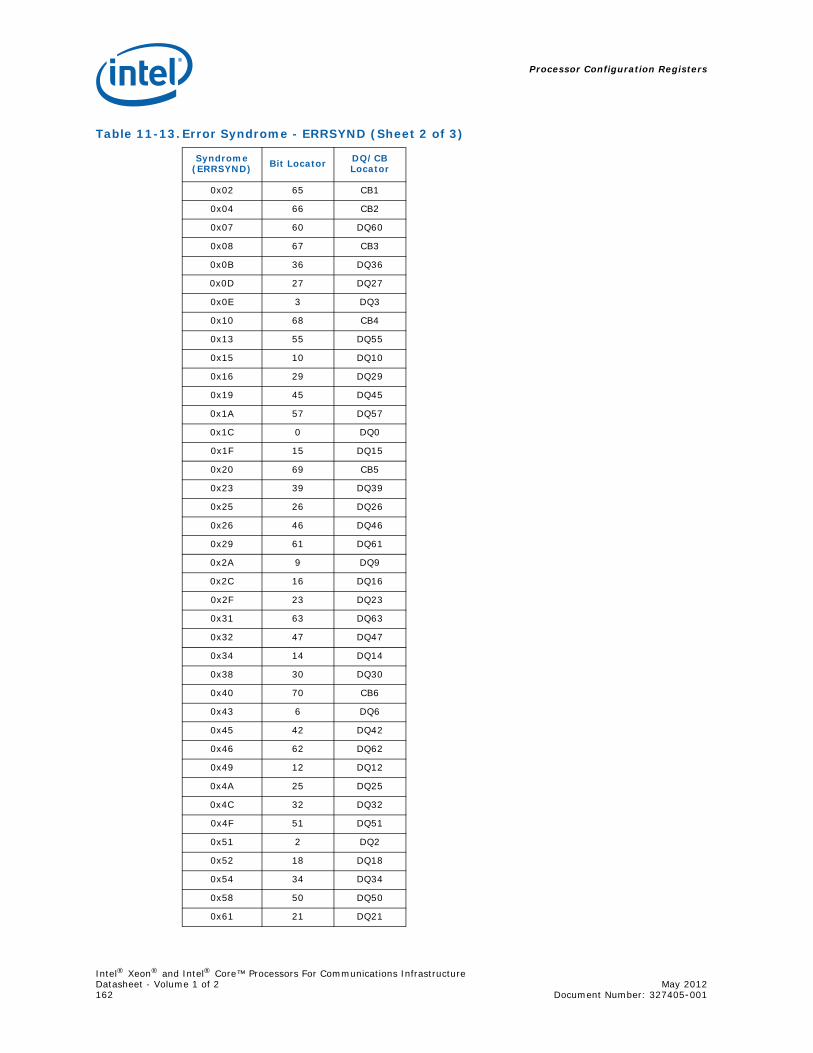
Processor Configuration Registers
Intel® Xeon® and Intel® Core™ Processors For Communications InfrastructureDatasheet - Volume 1 of 2 May 2012162 Document Number: 327405-001
0x02 65 CB1
0x04 66 CB2
0x07 60 DQ60
0x08 67 CB3
0x0B 36 DQ36
0x0D 27 DQ27
0x0E 3 DQ3
0x10 68 CB4
0x13 55 DQ55
0x15 10 DQ10
0x16 29 DQ29
0x19 45 DQ45
0x1A 57 DQ57
0x1C 0 DQ0
0x1F 15 DQ15
0x20 69 CB5
0x23 39 DQ39
0x25 26 DQ26
0x26 46 DQ46
0x29 61 DQ61
0x2A 9 DQ9
0x2C 16 DQ16
0x2F 23 DQ23
0x31 63 DQ63
0x32 47 DQ47
0x34 14 DQ14
0x38 30 DQ30
0x40 70 CB6
0x43 6 DQ6
0x45 42 DQ42
0x46 62 DQ62
0x49 12 DQ12
0x4A 25 DQ25
0x4C 32 DQ32
0x4F 51 DQ51
0x51 2 DQ2
0x52 18 DQ18
0x54 34 DQ34
0x58 50 DQ50
0x61 21 DQ21
Table 11-13.Error Syndrome - ERRSYND (Sheet 2 of 3)
Syndrome(ERRSYND) Bit Locator DQ/CB
Locator
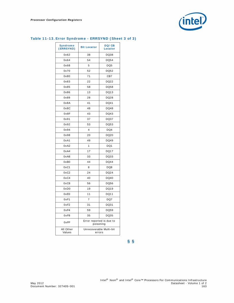
Processor Configuration Registers
Intel® Xeon® and Intel® Core™ Processors For Communications InfrastructureMay 2012 Datasheet - Volume 1 of 2Document Number: 327405-001 163
§ §
0x62 38 DQ38
0x64 54 DQ54
0x68 5 DQ5
0x70 52 DQ52
0x80 71 CB7
0x83 22 DQ22
0x85 58 DQ58
0x86 13 DQ13
0x89 28 DQ28
0x8A 41 DQ41
0x8C 48 DQ48
0x8F 43 DQ43
0x91 37 DQ37
0x92 53 DQ53
0x94 4 DQ4
0x98 20 DQ20
0xA1 49 DQ49
0xA2 1 DQ1
0xA4 17 DQ17
0xA8 33 DQ33
0xB0 44 DQ44
0xC1 8 DQ8
0xC2 24 DQ24
0xC4 40 DQ40
0xC8 56 DQ56
0xD0 19 DQ19
0xE0 11 DQ11
0xF1 7 DQ7
0xF2 31 DQ31
0xF4 59 DQ59
0xF8 35 DQ35
0xFF Error reported is due to poisoning
All Other Values
Unrecoverable Multi-bit errors
Table 11-13.Error Syndrome - ERRSYND (Sheet 3 of 3)
Syndrome(ERRSYND) Bit Locator DQ/CB
Locator

Processor Configuration Registers
Intel® Xeon® and Intel® Core™ Processors For Communications InfrastructureDatasheet - Volume 1 of 2 May 2012164 Document Number: 327405-001