Embed Size (px)
Citation preview
Intel® Open Source HD Graphics Programmers' Reference Manual (PRM)
Volume 4: Configurations
For the 2014-2015 Intel Atom™ Processors, Celeron™ Processors and Pentium™ Processors based on the "Cherry Trail/Braswell" Platform (Cherryview/Braswell graphics)
June 2015, Revision 1.0

Configurations
ii Doc Ref # IHD-OS-CHV-BSW-Vol 4-06.15
Creative Commons License
You are free to Share - to copy, distribute, display, and perform the work under the following conditions:
• Attribution. You must attribute the work in the manner specified by the author or licensor (but not in any way that suggests that they endorse you or your use of the work).
• No Derivative Works. You may not alter, transform, or build upon this work.
Notices and Disclaimers
INFORMATION IN THIS DOCUMENT IS PROVIDED IN CONNECTION WITH INTEL® PRODUCTS. NO LICENSE, EXPRESS OR IMPLIED, BY ESTOPPEL OR OTHERWISE, TO ANY INTELLECTUAL PROPERTY RIGHTS IS GRANTED BY THIS DOCUMENT. EXCEPT AS PROVIDED IN INTEL'S TERMS AND CONDITIONS OF SALE FOR SUCH PRODUCTS, INTEL ASSUMES NO LIABILITY WHATSOEVER AND INTEL DISCLAIMS ANY EXPRESS OR IMPLIED WARRANTY, RELATING TO SALE AND/OR USE OF INTEL PRODUCTS INCLUDING LIABILITY OR WARRANTIES RELATING TO FITNESS FOR A PARTICULAR PURPOSE, MERCHANTABILITY, OR INFRINGEMENT OF ANY PATENT, COPYRIGHT OR OTHER INTELLECTUAL PROPERTY RIGHT.
A "Mission Critical Application" is any application in which failure of the Intel Product could result, directly or indirectly, in personal injury or death. SHOULD YOU PURCHASE OR USE INTEL'S PRODUCTS FOR ANY SUCH MISSION CRITICAL APPLICATION, YOU SHALL INDEMNIFY AND HOLD INTEL AND ITS SUBSIDIARIES, SUBCONTRACTORS AND AFFILIATES, AND THE DIRECTORS, OFFICERS, AND EMPLOYEES OF EACH, HARMLESS AGAINST ALL CLAIMS COSTS, DAMAGES, AND EXPENSES AND REASONABLE ATTORNEYS' FEES ARISING OUT OF, DIRECTLY OR INDIRECTLY, ANY CLAIM OF PRODUCT LIABILITY, PERSONAL INJURY, OR DEATH ARISING IN ANY WAY OUT OF SUCH MISSION CRITICAL APPLICATION, WHETHER OR NOT INTEL OR ITS SUBCONTRACTOR WAS NEGLIGENT IN THE DESIGN, MANUFACTURE, OR WARNING OF THE INTEL PRODUCT OR ANY OF ITS PARTS.
Intel may make changes to specifications and product descriptions at any time, without notice. Designers must not rely on the absence or characteristics of any features or instructions marked "reserved" or "undefined". Intel reserves these for future definition and shall have no responsibility whatsoever for conflicts or incompatibilities arising from future changes to them. The information here is subject to change without notice. Do not finalize a design with this information.
The products described in this document may contain design defects or errors known as errata which may cause the product to deviate from published specifications. Current characterized errata are available on request.
Implementations of the I2C bus/protocol may require licenses from various entities, including Philips Electronics N.V. and North American Philips Corporation.
Intel and the Intel logo are trademarks of Intel Corporation in the U.S. and other countries.
* Other names and brands may be claimed as the property of others.
Copyright © 2015, Intel Corporation. All rights reserved.

Configurations
Doc Ref # IHD-OS-CHV-BSW-Vol 4-06.15 iii
Table of Contents
Configurations Overview ............................................................................................................. 1
Configurations ............................................................................................................................... 1
Top Level Block Diagrams ................................................................................................................................... 2
Device Attributes .................................................................................................................................................... 5

Configurations
Doc Ref # IHD-OS-CHV-BSW-Vol 4-06.15 1
Configurations Overview The Intel "Gen" Graphics Architecture was first introduced to the market in 2004. Since that time, the architecture and its implementation have evolved to add many new features, increase performance, and improve power efficiency. This volume of the PRM tracks the Gen graphics evolution. It also provides information over time about changes to architectural attributes, feature sets, and performance.
Configurations This chapter contains configurations details as described in the following sections:
• Top Level Block Diagrams • Device Attributes

Configurations
2 Doc Ref # IHD-OS-CHV-BSW-Vol 4-06.15
Top Level Block Diagrams
The diagram below shows basic feature blocks of the Cherryview (CHV) graphics architecture:
Configurations
Doc Ref # IHD-OS-CHV-BSW-Vol 4-06.15 3
This diagram is based on the following functional partitions:
(a) Geometry Fixed Functions (Geom/FF)
(b) Media Fixed Functions (Media/FF)
(c) Global Assets and GT Interface (GA)
(d) One or more Subslices (two shown)
(e) A Slice Common block
(f) An L3 Cache (L3$) block
Note that the combination of (a), (b), and (c) is typically referred to as the “unslice”, while a combination of (d), (e), and (f) is referred to as a compute “slice”.
The functionality in each of these groupings is further broken down as follows:
• Unslice – Fixed function pipelines for 3D, GPGPU, and Media operations, and interface to the outside world.
• The 3D Geometry / Fixed Function (Geom/FF) block consisting of: • 3D fixed function pipeline (CS, VFVS, HS, TE, DS, GS, SOL, SL, SFE, SVG) • Video Front-End unit (VFE) • Thread Spawner unit (TSG) and the global Thread Dispatcher unit (TDG) • Unified Return Buffer Manager (URBM)
• Media fixed function assets: • Video Decode (VD) Box • Video Encode (VE) Box
• The Global Assets (GA) block as the primary interface and memory stream gateway to the outside world, consisting of:
• GT Interface (GTI) • State Variable Manager (SVM) • Blitter (BLT) • Graphics Arbiter (GAM)
• Subslice (three shown) – A compute unit with supporting fixed- or shared-function assets sufficient for the EU capability.
• A bank of Execution Units (EUs) – eight per subslice shown • Sampler, supporting both media and 3D functions • Gateway (GWY) • Instruction cache (IC) • Local Thread Dispatcher (TDL) • Barycentric Calculator (BC) • Pixel Shader Dispatcher (PSD)

Configurations
4 Doc Ref # IHD-OS-CHV-BSW-Vol 4-06.15
• Data Cluster (HDC) • Dataport Render Cache (DAPRC) - two per subslice
• Slice Common – Scalable fixed function assets which support the compute horsepower provided two or more subslices.
• 3D Fixed Function: • Windower/Mask unit (WM) • Plane-Z, Hi-Z (HZ) and Intermediate Z (IZ) • Setup Backend (SBE) • Pixel backend units • 3D stream caches for color, multi-sample surface, iz, and stencil (RCC$, MSC$, HZ$,
RCZ$, STC$) • Media Fixed Function:
• DAPRSC • RCPFE, BE • SVL • TDC
• L3 Cache – backing L3 cache for certain memory streams emanating from subslices. • L3 Data cache with support for data, URB, and shared local memory (SLM)

Configurations
Doc Ref # IHD-OS-CHV-BSW-Vol 4-06.15 5
Device Attributes
Product Configuration Attribute Table
Product Family CHV
Architectural Name 2x4 2x6 2x8
SKU Name
Global Attributes
Slice count 1 1 1
Subslice Count 2 2 2
EU/Subslice 4 6 8
EU count (total) 8 12 16
Thread Count 7 7 7
Thread Count (Total) 56 84 112
FLOPs/Clk - Half Precision, MAD (peak) 256 384 512
FLOPs/Clk - Single Precision, MAD (peak) 128 192 256
FLOPs/Clk - Double Precision, MAD (peak) 16 24 32
Unslice clocking (coupled/decoupled from Cr slice) coupled [1]
coupled [1]
coupled [1]
GTI / Ring Interfaces 1 1 1
GTI bandwidth (bytes/unslice-clk) 64: R 64: R 64: R
64: W 64: W 64: W
Caches & Dedicated Memories
L3 Cache, total size (bytes) 384K 384K 384K
L3 Cache, bank count 2 2 2
L3 Cache, bandwidth (bytes/clk)
L3 Cache, D$ Size (Kbytes) 192K-256K 192K-256K 192K-256K
URB Size (kbytes) 64K-192K 64K-192K 64K-192K
SLM Size (kbytes) 0, 128K 0, 128K 0, 128K
LLC/L4 size (bytes) N/A N/A N/A
Instruction Cache (IC, bytes) 2x 48K 2x 48K 2x 48K
Color Cache (RCC, bytes) 24K 24K 24K
MSC Cache (MSC, bytes) 12K 12K 12K
HiZ Cache (HZC, bytes) 8K 8K 8K
Z Cache (RCZ, bytes) 16K 16K 16K
Stencil Cache (STC, bytes) 4K 4K 4K
L1 Texture Cache (bytes) 2x 32K 2x 32K 2x 32K
MT Texture Cache (bytes) 2x 8K 2x 8K 2x 8K
Configurations
6 Doc Ref # IHD-OS-CHV-BSW-Vol 4-06.15
Product Configuration Attribute Table
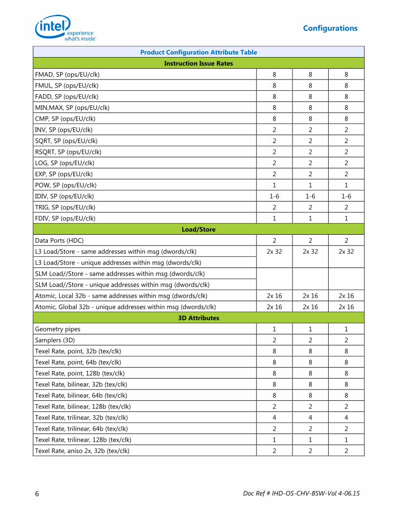
Instruction Issue Rates
FMAD, SP (ops/EU/clk) 8 8 8
FMUL, SP (ops/EU/clk) 8 8 8
FADD, SP (ops/EU/clk) 8 8 8
MIN,MAX, SP (ops/EU/clk) 8 8 8
CMP, SP (ops/EU/clk) 8 8 8
INV, SP (ops/EU/clk) 2 2 2
SQRT, SP (ops/EU/clk) 2 2 2
RSQRT, SP (ops/EU/clk) 2 2 2
LOG, SP (ops/EU/clk) 2 2 2
EXP, SP (ops/EU/clk) 2 2 2
POW, SP (ops/EU/clk) 1 1 1
IDIV, SP (ops/EU/clk) 1-6 1-6 1-6
TRIG, SP (ops/EU/clk) 2 2 2
FDIV, SP (ops/EU/clk) 1 1 1
Load/Store
Data Ports (HDC) 2 2 2
L3 Load/Store - same addresses within msg (dwords/clk) 2x 32 2x 32 2x 32
L3 Load/Store - unique addresses within msg (dwords/clk)
SLM Load//Store - same addresses within msg (dwords/clk)
SLM Load//Store - unique addresses within msg (dwords/clk)
Atomic, Local 32b - same addresses within msg (dwords/clk) 2x 16 2x 16 2x 16
Atomic, Global 32b - unique addresses within msg (dwords/clk) 2x 16 2x 16 2x 16
3D Attributes
Geometry pipes 1 1 1
Samplers (3D) 2 2 2
Texel Rate, point, 32b (tex/clk) 8 8 8
Texel Rate, point, 64b (tex/clk) 8 8 8
Texel Rate, point, 128b (tex/clk) 8 8 8
Texel Rate, bilinear, 32b (tex/clk) 8 8 8
Texel Rate, bilinear, 64b (tex/clk) 8 8 8
Texel Rate, bilinear, 128b (tex/clk) 2 2 2
Texel Rate, trilinear, 32b (tex/clk) 4 4 4
Texel Rate, trilinear, 64b (tex/clk) 2 2 2
Texel Rate, trilinear, 128b (tex/clk) 1 1 1
Texel Rate, aniso 2x, 32b (tex/clk) 2 2 2
Configurations
Doc Ref # IHD-OS-CHV-BSW-Vol 4-06.15 7
Product Configuration Attribute Table
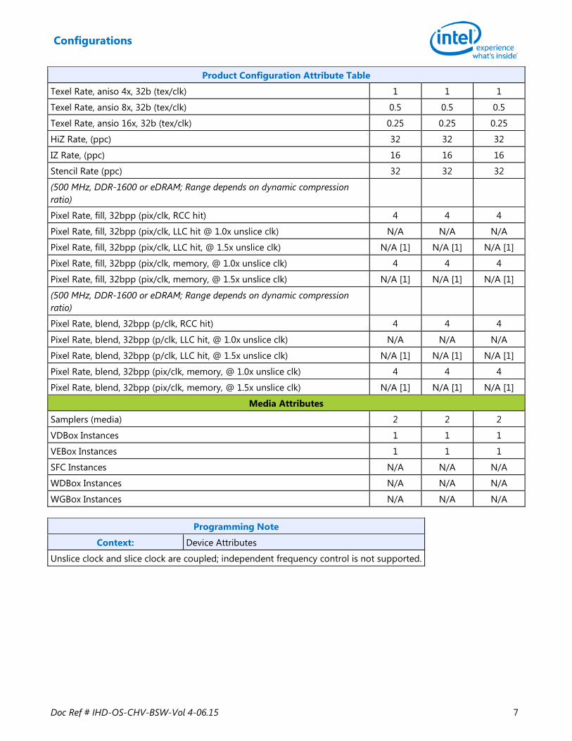
Texel Rate, aniso 4x, 32b (tex/clk) 1 1 1
Texel Rate, ansio 8x, 32b (tex/clk) 0.5 0.5 0.5
Texel Rate, ansio 16x, 32b (tex/clk) 0.25 0.25 0.25
HiZ Rate, (ppc) 32 32 32
IZ Rate, (ppc) 16 16 16
Stencil Rate (ppc) 32 32 32
(500 MHz, DDR-1600 or eDRAM; Range depends on dynamic compression ratio)
Pixel Rate, fill, 32bpp (pix/clk, RCC hit) 4 4 4
Pixel Rate, fill, 32bpp (pix/clk, LLC hit @ 1.0x unslice clk) N/A N/A N/A
Pixel Rate, fill, 32bpp (pix/clk, LLC hit, @ 1.5x unslice clk) N/A [1] N/A [1] N/A [1]
Pixel Rate, fill, 32bpp (pix/clk, memory, @ 1.0x unslice clk) 4 4 4
Pixel Rate, fill, 32bpp (pix/clk, memory, @ 1.5x unslice clk) N/A [1] N/A [1] N/A [1]
(500 MHz, DDR-1600 or eDRAM; Range depends on dynamic compression ratio)
Pixel Rate, blend, 32bpp (p/clk, RCC hit) 4 4 4
Pixel Rate, blend, 32bpp (p/clk, LLC hit, @ 1.0x unslice clk) N/A N/A N/A
Pixel Rate, blend, 32bpp (p/clk, LLC hit, @ 1.5x unslice clk) N/A [1] N/A [1] N/A [1]
Pixel Rate, blend, 32bpp (pix/clk, memory, @ 1.0x unslice clk) 4 4 4
Pixel Rate, blend, 32bpp (pix/clk, memory, @ 1.5x unslice clk) N/A [1] N/A [1] N/A [1]
Media Attributes
Samplers (media) 2 2 2
VDBox Instances 1 1 1
VEBox Instances 1 1 1
SFC Instances N/A N/A N/A
WDBox Instances N/A N/A N/A
WGBox Instances N/A N/A N/A
Programming Note
Context: Device Attributes
Unslice clock and slice clock are coupled; independent frequency control is not supported.


![WHY GRAPHICS PROGRAMMERS NEED TO KNOW ...[Aila et al. 2010] AILA, T., AND KARRAS, T. 2010. Architecture considerations for tracing incoherent rays. In Proc. High Performance Graphics](https://img.dokumen.tips/doc/110x75/61468b027599b83a5f004a14/why-graphics-programmers-need-to-know-aila-et-al-2010-aila-t-and-karras.jpg)