Embed Size (px)
Citation preview

Intel® MAX® 10 High-Speed LVDSI/O User Guide
Updated for Intel® Quartus® Prime Design Suite: 17.1
SubscribeSend Feedback
UG-M10LVDS | 2017.12.15Latest document on the web: PDF | HTML

Contents
1 Intel® MAX® 10 High-Speed LVDS I/O Overview............................................................. 41.1 Altera Soft LVDS Implementation Overview................................................................ 4
2 Intel MAX 10 High-Speed LVDS Architecture and Features.............................................. 62.1 Intel MAX 10 LVDS Channels Support ...................................................................... 62.2 Intel MAX 10 LVDS SERDES I/O Standards Support................................................... 112.3 Intel MAX 10 High-Speed LVDS Circuitry.................................................................. 122.4 Intel MAX 10 High-Speed LVDS I/O Location.............................................................132.5 Differential I/O Pins in Low Speed Region.................................................................15
3 Intel MAX 10 LVDS Transmitter Design.......................................................................... 163.1 High-Speed I/O Transmitter Circuitry......................................................................163.2 LVDS Transmitter Programmable I/O Features.......................................................... 16
3.2.1 Programmable Pre-Emphasis...................................................................... 163.2.2 Programmable Differential Output Voltage.................................................... 17
3.3 LVDS Transmitter I/O Termination Schemes..............................................................183.3.1 Emulated LVDS External Termination........................................................... 183.3.2 Sub-LVDS Transmitter External Termination..................................................183.3.3 SLVS Transmitter External Termination.........................................................193.3.4 Emulated RSDS, Emulated Mini-LVDS, and Emulated PPDS Transmitter
External Termination................................................................................ 193.4 LVDS Transmitter FPGA Design Implementation........................................................ 20
3.4.1 Altera Soft LVDS IP Core in Transmitter Mode............................................... 203.4.2 High-Speed I/O Timing Budget................................................................... 233.4.3 Guidelines: LVDS Transmitter Channels Placement.........................................233.4.4 Guidelines: LVDS Channels PLL Placement....................................................243.4.5 Guidelines: LVDS Transmitter Logic Placement.............................................. 243.4.6 Guidelines: Enable LVDS Pre-Emphasis for E144 Package............................... 24
3.5 LVDS Transmitter Debug and Troubleshooting........................................................... 253.5.1 Perform RTL Simulation Before Hardware Debug........................................... 253.5.2 Geometry-Based and Physics-Based I/O Rules.............................................. 25
4 Intel MAX 10 LVDS Receiver Design...............................................................................264.1 High-Speed I/O Receiver Circuitry........................................................................... 26
4.1.1 Soft Deserializer....................................................................................... 264.1.2 Data Realignment Block (Bit Slip)................................................................27
4.2 LVDS Receiver I/O Termination Schemes..................................................................274.2.1 LVDS, Mini-LVDS, and RSDS Receiver External Termination.............................274.2.2 SLVS Receiver External Termination.............................................................284.2.3 Sub-LVDS Receiver External Termination......................................................284.2.4 TMDS Receiver External Termination............................................................294.2.5 HiSpi Receiver External Termination.............................................................294.2.6 LVPECL External Termination...................................................................... 30
4.3 LVDS Receiver FPGA Design Implementation............................................................ 314.3.1 Altera Soft LVDS IP Core in Receiver Mode................................................... 314.3.2 High-Speed I/O Timing Budget................................................................... 344.3.3 Guidelines: Floating LVDS Input Pins........................................................... 374.3.4 Guidelines: LVDS Receiver Channels Placement.............................................37
Contents
Intel® MAX® 10 High-Speed LVDS I/O User Guide2

4.3.5 Guidelines: LVDS Channels PLL Placement....................................................384.3.6 Guidelines: LVDS Receiver Logic Placement.................................................. 38
4.4 LVDS Receiver Debug and Troubleshooting............................................................... 384.4.1 Perform RTL Simulation Before Hardware Debug........................................... 394.4.2 Geometry-Based and Physics-Based I/O Rules.............................................. 39
5 Intel MAX 10 LVDS Transmitter and Receiver Design.....................................................405.1 Transmitter–Receiver Interfacing.............................................................................405.2 LVDS Transmitter and Receiver FPGA Design Implementation......................................41
5.2.1 LVDS Transmitter and Receiver PLL Sharing Implementation........................... 415.2.2 Initializing the Altera Soft LVDS IP Core....................................................... 42
5.3 LVDS Transmitter and Receiver Debug and Troubleshooting........................................ 425.3.1 Perform RTL Simulation Before Hardware Debug........................................... 425.3.2 Geometry-Based and Physics-Based I/O Rules.............................................. 42
6 Intel MAX 10 High-Speed LVDS Board Design Considerations........................................ 436.1 Guidelines: Improve Signal Quality..........................................................................436.2 Guidelines: Control Channel-to-Channel Skew.......................................................... 436.3 Guidelines: Determine Board Design Constraints.......................................................446.4 Guidelines: Perform Board Level Simulations............................................................ 44
7 Altera Soft LVDS IP Core References..............................................................................467.1 Altera Soft LVDS Parameter Settings ......................................................................467.2 Altera Soft LVDS Interface Signals...........................................................................49
8 Intel MAX 10 High-Speed LVDS I/O User Guide Archives...............................................52
9 Document Revision History for Intel MAX 10 High-Speed LVDS I/O User Guide.............53
Contents
Intel® MAX® 10 High-Speed LVDS I/O User Guide3

1 Intel® MAX® 10 High-Speed LVDS I/O OverviewThe Intel® MAX® 10 device family supports high-speed LVDS protocols through theLVDS I/O banks and the Altera Soft LVDS IP core.
The LVDS I/O banks in Intel MAX 10 devices feature true and emulated LVDS buffers:
• True LVDS buffers support LVDS using true differential buffers.
• Emulated LVDS buffers use a pair of single-ended pins to emulate differentialbuffers.
Table 1. Summary of LVDS I/O Buffers Support in Intel MAX 10 I/O Banks
I/O Buffer Type I/O Bank Support
True LVDS input buffer All I/O banks
True LVDS output buffer Only bottom I/O banks
Emulated LVDS output buffer All I/O banks
The Intel MAX 10 D (dual supply) and S (single supply) device variants supportdifferent LVDS I/O standards. For a list of LVDS I/O standards supported by the IntelMAX 10 D and S variants, refer to the related information.
Related Links
• Intel MAX 10 High-Speed LVDS Architecture and Features on page 6Provides information about the high-speed LVDS architecture and the featuressupported by the device.
• Altera Soft LVDS IP Core References on page 46Lists the parameters and signals of Altera Soft LVDS IP core for Intel MAX 10devices.
• Intel MAX 10 LVDS SERDES I/O Standards Support on page 11Lists the supported LVDS I/O standards and the support in different Intel MAX10 device variants.
• Intel MAX 10 High-Speed LVDS I/O User Guide Archives on page 52Provides a list of user guides for previous versions of the Altera Soft LVDS IPcore.
1.1 Altera Soft LVDS Implementation Overview
You can implement LVDS applications in Intel MAX 10 devices as transmitter-only,receiver-only, or a combination of transmitters and receivers.
UG-M10LVDS | 2017.12.15
Intel Corporation. All rights reserved. Intel, the Intel logo, Altera, Arria, Cyclone, Enpirion, MAX, Nios, Quartusand Stratix words and logos are trademarks of Intel Corporation or its subsidiaries in the U.S. and/or othercountries. Intel warrants performance of its FPGA and semiconductor products to current specifications inaccordance with Intel's standard warranty, but reserves the right to make changes to any products and servicesat any time without notice. Intel assumes no responsibility or liability arising out of the application or use of anyinformation, product, or service described herein except as expressly agreed to in writing by Intel. Intelcustomers are advised to obtain the latest version of device specifications before relying on any publishedinformation and before placing orders for products or services.*Other names and brands may be claimed as the property of others.
ISO9001:2008Registered

Figure 1. Intel MAX 10 LVDS Implementation Overview
Altera Soft LVDS
LVDS TransmitterImplementation
LVDS Transmitterand Receiver
Implementation
LVDS ReceiverImplementation
Related Links
• Intel MAX 10 LVDS Transmitter Design on page 16Provides information and guidelines for implementing LVDS transmitter in IntelMAX 10 devices using the Altera Soft LVDS IP core.
• Intel MAX 10 LVDS Receiver Design on page 26Provides information and guidelines for implementing LVDS receiver in IntelMAX 10 devices using the Altera Soft LVDS IP core.
• Intel MAX 10 LVDS Transmitter and Receiver Design on page 40Provides design guidelines for implementing both LVDS transmitters andreceivers in the same Intel MAX 10 device.
1 Intel® MAX® 10 High-Speed LVDS I/O Overview
UG-M10LVDS | 2017.12.15
Intel® MAX® 10 High-Speed LVDS I/O User Guide5

2 Intel MAX 10 High-Speed LVDS Architecture andFeatures
The Intel MAX 10 devices use registers and logic in the core fabric to implement LVDSinput and output interfaces.
• For LVDS transmitters and receivers, Intel MAX 10 devices use the the double datarate I/O (DDIO) registers that reside in the I/O elements (IOE). This architectureimproves performance with regards to the receiver input skew margin (RSKM) ortransmitter channel-to-channel skew (TCCS).
• For the LVDS serializer/deserializer (SERDES), Intel MAX 10 devices use logicelements (LE) registers.
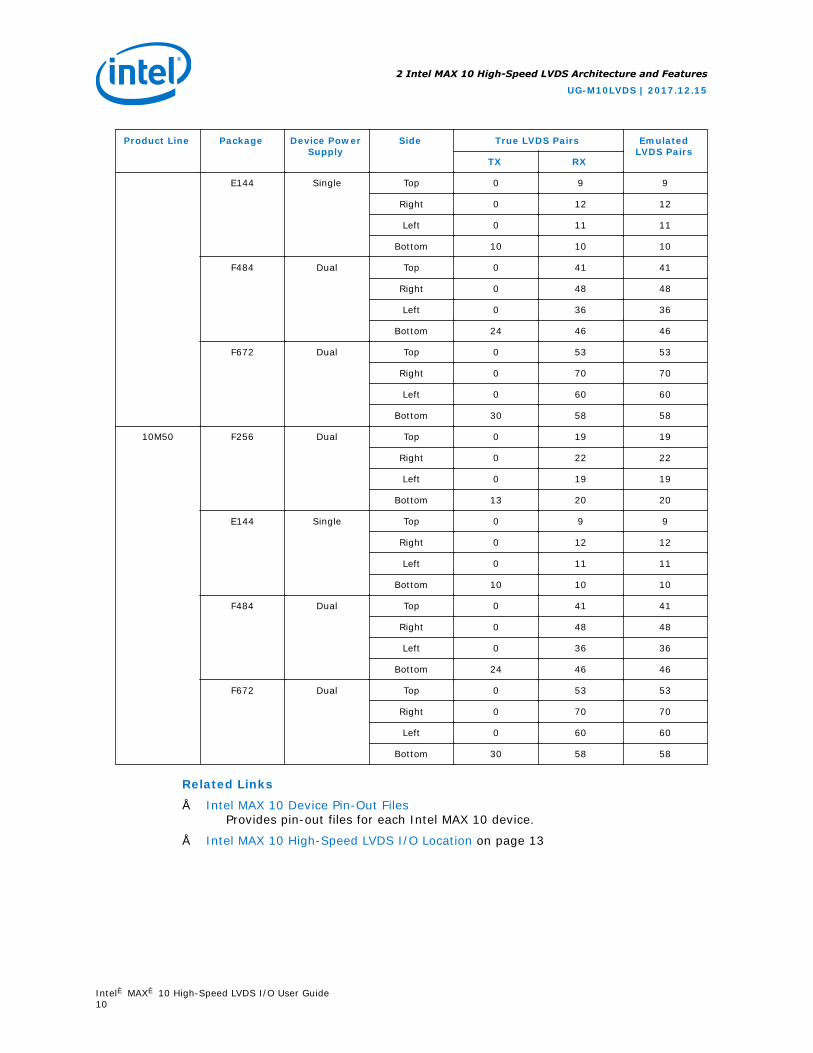
2.1 Intel MAX 10 LVDS Channels Support
The LVDS channels available vary among Intel MAX 10 devices. All I/O banks in IntelMAX 10 devices support true LVDS input buffers and emulated LVDS output buffers.However, only the bottom I/O banks support true LVDS output buffers.
Table 2. LVDS Buffers in Intel MAX 10 DevicesThis table lists the LVDS buffer support for I/O banks on each side of the devices.
Product Line Package Device PowerSupply
Side True LVDS Pairs EmulatedLVDS Pairs
TX RX
10M02 V36 Dual Top 0 1 1
Right 0 3 3
Left 0 3 3
Bottom 3 3 3
M153 Single Top 0 12 12
Right 0 12 12
Left 0 12 12
Bottom 9 13 13
U169 Single Top 0 12 12
Right 0 17 17
Left 0 15 15
Bottom 9 14 14
U324 Single Top 0 27 27
Right 0 31 31
Left 0 28 28
continued...
UG-M10LVDS | 2017.12.15
Intel Corporation. All rights reserved. Intel, the Intel logo, Altera, Arria, Cyclone, Enpirion, MAX, Nios, Quartusand Stratix words and logos are trademarks of Intel Corporation or its subsidiaries in the U.S. and/or othercountries. Intel warrants performance of its FPGA and semiconductor products to current specifications inaccordance with Intel's standard warranty, but reserves the right to make changes to any products and servicesat any time without notice. Intel assumes no responsibility or liability arising out of the application or use of anyinformation, product, or service described herein except as expressly agreed to in writing by Intel. Intelcustomers are advised to obtain the latest version of device specifications before relying on any publishedinformation and before placing orders for products or services.*Other names and brands may be claimed as the property of others.
ISO9001:2008Registered

Product Line Package Device PowerSupply
Side True LVDS Pairs EmulatedLVDS Pairs
TX RX
Bottom 15 28 28
Dual Top 0 13 13
Right 0 24 24
Left 0 20 20
Bottom 9 16 16
E144 Single Top 0 10 10
Right 0 12 12
Left 0 11 11
Bottom 7 12 12
10M04 M153 Single Top 0 12 12
Right 0 12 12
Left 0 12 12
Bottom 9 13 13
U169 Single Top 0 12 12
Right 0 17 17
Left 0 15 15
Bottom 9 14 14
U324 Single Top 0 27 27
Right 0 31 31
Left 0 28 28
Bottom 15 28 28
Dual Top 0 27 27
Right 0 31 31
Left 0 28 28
Bottom 15 28 28
F256 Dual Top 0 19 19
Right 0 22 22
Left 0 19 19
Bottom 13 20 20
E144 Single Top 0 8 8
Right 0 12 12
Left 0 11 11
Bottom 10 10 10
10M08 V81 Dual Top 0 5 5
Right 0 7 7
continued...
2 Intel MAX 10 High-Speed LVDS Architecture and Features
UG-M10LVDS | 2017.12.15
Intel® MAX® 10 High-Speed LVDS I/O User Guide7

Product Line Package Device PowerSupply
Side True LVDS Pairs EmulatedLVDS Pairs
TX RX
Left 0 6 6
Bottom 7 7 7
M153 Single Top 0 12 12
Right 0 12 12
Left 0 12 12
Bottom 9 13 13
U169 Single Top 0 12 12
Right 0 17 17
Left 0 15 15
Bottom 9 14 14
U324 Single Top 0 27 27
Right 0 31 31
Left 0 28 28
Bottom 15 28 28
Dual Top 0 27 27
Right 0 31 31
Left 0 28 28
Bottom 15 28 28
F256 Dual Top 0 19 19
Right 0 22 22
Left 0 19 19
Bottom 13 20 20
E144 Single Top 0 8 8
Right 0 12 12
Left 0 11 11
Bottom 10 10 10
F484 Dual Top 0 27 27
Right 0 33 33
Left 0 28 28
Bottom 15 28 28
10M16 U169 Single Top 0 12 12
Right 0 17 17
Left 0 15 15
Bottom 9 14 14
U324 Single Top 0 27 27
continued...
2 Intel MAX 10 High-Speed LVDS Architecture and Features
UG-M10LVDS | 2017.12.15
Intel® MAX® 10 High-Speed LVDS I/O User Guide8

Product Line Package Device PowerSupply
Side True LVDS Pairs EmulatedLVDS Pairs
TX RX
Right 0 31 31
Left 0 28 28
Bottom 15 28 28
Dual Top 0 27 27
Right 0 31 31
Left 0 28 28
Bottom 15 28 28
F256 Dual Top 0 19 19
Right 0 22 22
Left 0 19 19
Bottom 13 20 20
E144 Single Top 0 8 8
Right 0 12 12
Left 0 11 11
Bottom 10 10 10
F484 Dual Top 0 39 39
Right 0 38 38
Left 0 32 32
Bottom 22 42 42
10M25 F256 Dual Top 0 19 19
Right 0 22 22
Left 0 19 19
Bottom 13 20 20
E144 Single Top 0 8 8
Right 0 12 12
Left 0 11 11
Bottom 10 10 10
F484 Dual Top 0 41 41
Right 0 48 48
Left 0 36 36
Bottom 24 46 46
10M40 F256 Dual Top 0 19 19
Right 0 22 22
Left 0 19 19
Bottom 13 20 20
continued...
2 Intel MAX 10 High-Speed LVDS Architecture and Features
UG-M10LVDS | 2017.12.15
Intel® MAX® 10 High-Speed LVDS I/O User Guide9
Product Line Package Device PowerSupply
Side True LVDS Pairs EmulatedLVDS Pairs
TX RX
E144 Single Top 0 9 9
Right 0 12 12
Left 0 11 11
Bottom 10 10 10
F484 Dual Top 0 41 41
Right 0 48 48
Left 0 36 36
Bottom 24 46 46
F672 Dual Top 0 53 53
Right 0 70 70
Left 0 60 60
Bottom 30 58 58
10M50 F256 Dual Top 0 19 19
Right 0 22 22
Left 0 19 19
Bottom 13 20 20
E144 Single Top 0 9 9
Right 0 12 12
Left 0 11 11
Bottom 10 10 10
F484 Dual Top 0 41 41
Right 0 48 48
Left 0 36 36
Bottom 24 46 46
F672 Dual Top 0 53 53
Right 0 70 70
Left 0 60 60
Bottom 30 58 58
Related Links
• Intel MAX 10 Device Pin-Out FilesProvides pin-out files for each Intel MAX 10 device.
• Intel MAX 10 High-Speed LVDS I/O Location on page 13
2 Intel MAX 10 High-Speed LVDS Architecture and Features
UG-M10LVDS | 2017.12.15
Intel® MAX® 10 High-Speed LVDS I/O User Guide10
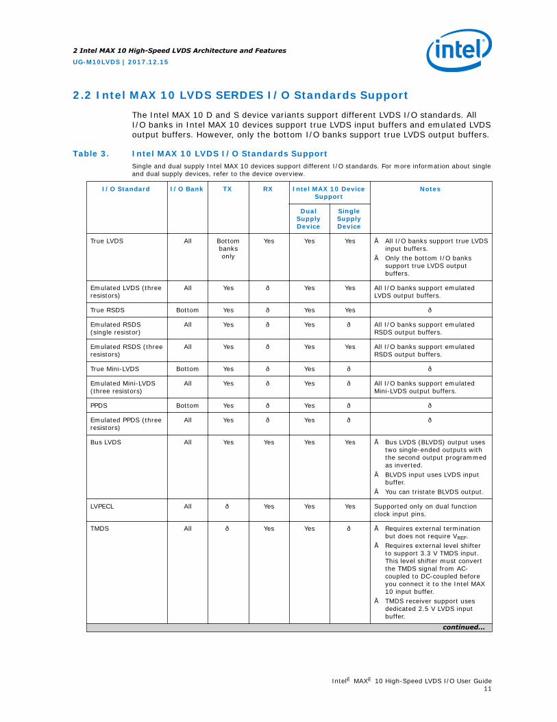
2.2 Intel MAX 10 LVDS SERDES I/O Standards Support
The Intel MAX 10 D and S device variants support different LVDS I/O standards. AllI/O banks in Intel MAX 10 devices support true LVDS input buffers and emulated LVDSoutput buffers. However, only the bottom I/O banks support true LVDS output buffers.
Table 3. Intel MAX 10 LVDS I/O Standards SupportSingle and dual supply Intel MAX 10 devices support different I/O standards. For more information about singleand dual supply devices, refer to the device overview.
I/O Standard I/O Bank TX RX Intel MAX 10 DeviceSupport
Notes
DualSupplyDevice
SingleSupplyDevice
True LVDS All Bottombanksonly
Yes Yes Yes • All I/O banks support true LVDSinput buffers.
• Only the bottom I/O bankssupport true LVDS outputbuffers.
Emulated LVDS (threeresistors)
All Yes — Yes Yes All I/O banks support emulatedLVDS output buffers.
True RSDS Bottom Yes — Yes Yes —
Emulated RSDS(single resistor)
All Yes — Yes — All I/O banks support emulatedRSDS output buffers.
Emulated RSDS (threeresistors)
All Yes — Yes Yes All I/O banks support emulatedRSDS output buffers.
True Mini-LVDS Bottom Yes — Yes — —
Emulated Mini-LVDS(three resistors)
All Yes — Yes — All I/O banks support emulatedMini-LVDS output buffers.
PPDS Bottom Yes — Yes — —
Emulated PPDS (threeresistors)
All Yes — Yes — —
Bus LVDS All Yes Yes Yes Yes • Bus LVDS (BLVDS) output usestwo single-ended outputs withthe second output programmedas inverted.
• BLVDS input uses LVDS inputbuffer.
• You can tristate BLVDS output.
LVPECL All — Yes Yes Yes Supported only on dual functionclock input pins.
TMDS All — Yes Yes — • Requires external terminationbut does not require VREF.
• Requires external level shifterto support 3.3 V TMDS input.This level shifter must convertthe TMDS signal from AC-coupled to DC-coupled beforeyou connect it to the Intel MAX10 input buffer.
• TMDS receiver support usesdedicated 2.5 V LVDS inputbuffer.
continued...
2 Intel MAX 10 High-Speed LVDS Architecture and Features
UG-M10LVDS | 2017.12.15
Intel® MAX® 10 High-Speed LVDS I/O User Guide11

I/O Standard I/O Bank TX RX Intel MAX 10 DeviceSupport
Notes
DualSupplyDevice
SingleSupplyDevice
Sub-LVDS All Yes Yes Yes — • Transmitter supports onlyemulated Sub-LVDS usingemulated 1.8 V differentialsignal as output.
• Requires external outputtermination.
• Does not require VREF.• Sub-LVDS receiver support
uses dedicated 2.5 V LVDSinput buffer.
SLVS All Yes Yes Yes — • SLVS transmitter support usesemulated LVDS output.
• Requires external terminationbut does not require VREF.
• SLVS receiver support usesdedicated 2.5 V LVDS inputbuffer.
HiSpi All — Yes Yes — • Only input is supportedbecause HiSpi is aunidirectional I/O standard.
• Requires external terminationbut does not require VREF.
• HiSpi receiver support usesdedicated 2.5 V LVDS inputbuffer.
Related Links
• Intel MAX 10 FPGA Device Overview
• Emulated LVDS External Termination on page 18
• Emulated RSDS, Emulated Mini-LVDS, and Emulated PPDS Transmitter ExternalTermination on page 19
• TMDS Receiver External Termination on page 29
• Sub-LVDS Transmitter External Termination on page 18
• Sub-LVDS Receiver External Termination on page 28
• SLVS Transmitter External Termination on page 19
• SLVS Receiver External Termination on page 28
• HiSpi Receiver External Termination on page 29
2.3 Intel MAX 10 High-Speed LVDS Circuitry
The LVDS solution uses the I/O elements and registers in the Intel MAX 10 devices.The Altera Soft LVDS IP core implements the serializer and deserializer as soft SERDESblocks in the core logic.
2 Intel MAX 10 High-Speed LVDS Architecture and Features
UG-M10LVDS | 2017.12.15
Intel® MAX® 10 High-Speed LVDS I/O User Guide12

The Intel MAX 10 devices do not contain dedicated serialization or deserializationcircuitry:
• You can use I/O pins and core fabric to implement a high-speed differentialinterface in the device.
• The Intel MAX 10 solution uses shift registers, internal PLLs, and I/O elements toperform the serial-to-parallel and parallel-to-serial conversions of incoming andoutgoing data.
• The Intel Quartus® Prime software uses the parameter settings of the Altera SoftLVDS IP core to automatically construct the differential SERDES in the core fabric.
Figure 2. Soft LVDS SERDESThis figure shows a transmitter and receiver block diagram for the soft LVDS SERDES circuitry with theinterface signals of the transmitter and receiver data paths.
FPGAFabric
rx_out
tx_in
rx_outclock
tx_coreclock10 bits
maximumdata width
+–
+–
tx_out
rx_in
10
10
pll_areset
rx_inclock / tx_inclockC0
C0
C0
C1
C1
C1
inclock
areset
ALTPLL
ALTERA_SOFT_LVDS
tx_in tx_out
inclock
ALTERA_SOFT_LVDS
rx_out rx_in
inclock
LVDS Transmitter
LVDS Receiver
Related Links
Intel MAX 10 Clocking and PLL User GuideProvides more information about the PLL and the PLL output counters.
2.4 Intel MAX 10 High-Speed LVDS I/O Location
The I/O banks in Intel MAX 10 devices support true LVDS input and emulated LVDSoutput on all I/O banks. Only the bottom I/O banks support true LVDS output.
2 Intel MAX 10 High-Speed LVDS Architecture and Features
UG-M10LVDS | 2017.12.15
Intel® MAX® 10 High-Speed LVDS I/O User Guide13

Figure 3. LVDS Support in I/O Banks of 10M02 Devices (Except Single Power SupplyU324 Package)This figure shows a top view of the silicon die. Each bank is labeled with the actual bank number. LVPECLsupport only in banks 2 and 6.
1
2 5
6
3
8
LVDSEmulated LVDS
RSDSEmulated RSDS
Mini-LVDSEmulated Mini-LVDS
PPDSEmulated PPDS
BLVDSLVPECL
TMDSSub-LVDS
SLVSHiSpi
TX RX
Figure 4. LVDS Support in I/O Banks of 10M02 (Single Power Supply U324 Package),10M04, and 10M08 DevicesThis figure shows a top view of the silicon die. Each bank is labeled with the actual bank number. LVPECLsupport only in banks 2 and 6.
1B
1A
2 5
6
3 4
8 7
LVDSEmulated LVDS
RSDSEmulated RSDS
Mini-LVDSEmulated Mini-LVDS
PPDSEmulated PPDS
BLVDSLVPECL
TMDSSub-LVDS
SLVSHiSpi
TX RX
2 Intel MAX 10 High-Speed LVDS Architecture and Features
UG-M10LVDS | 2017.12.15
Intel® MAX® 10 High-Speed LVDS I/O User Guide14

Figure 5. LVDS Support in I/O Banks of 10M16, 10M25, 10M40, and 10M50 DevicesThis figure shows a top view of the silicon die. Each bank is labeled with the actual bank number. LVPECLsupport only in banks 2, 3, 6, and 8.
1B
1A
2
3 4
8 7
OCT
5
6
LVDSEmulated LVDS
RSDSEmulated RSDS
Mini-LVDSEmulated Mini-LVDS
PPDSEmulated PPDS
BLVDSLVPECL
TMDSSub-LVDS
SLVSHiSpi
TX RX
Related Links
• PLL SpecificationsProvides PLL performance information for Intel MAX 10 devices.
• High-Speed I/O SpecificationsProvides minimum and maximum data rates for different data widths in IntelMAX 10 devices.
2.5 Differential I/O Pins in Low Speed Region
Some of the differential I/O pins are located in the low speed region of the Intel MAX10 device.
• For each user I/O pin (excluding configuration pin) that you place in the low speedregion, the Intel Quartus Prime software generates an informational warningmessage.
• Refer to the device pinout to identify the low speed I/O pins.
• Refer to the device datasheet for the performance information of these I/O pins.
Related Links
• Intel MAX 10 Device Pin-Out FilesProvides pin-out files for each Intel MAX 10 device.
• Intel MAX 10 Device Datasheet
• MAX 10 I/O Banks Locations, MAX 10 General Purpose I/O User GuideShows the locations of the high speed and low speed I/O banks.
2 Intel MAX 10 High-Speed LVDS Architecture and Features
UG-M10LVDS | 2017.12.15
Intel® MAX® 10 High-Speed LVDS I/O User Guide15

3 Intel MAX 10 LVDS Transmitter DesignYou can implement transmitter-only applications using the Intel MAX 10 LVDSsolution. You can use the Altera Soft LVDS IP core to instantiate soft SERDES circuitry.The soft SERDES circuitry works with the clocks and differential I/O pins to create ahigh-speed differential transmitter circuit.
3.1 High-Speed I/O Transmitter Circuitry
The LVDS transmitter circuitry uses the I/O elements and registers in the Intel MAX 10devices. The Altera Soft LVDS IP core implements the serializer as a soft SERDESblock in the core logic.
Related Links
Intel MAX 10 High-Speed LVDS Circuitry on page 12
3.2 LVDS Transmitter Programmable I/O Features
You can program some features of the I/O buffers and pins in Intel MAX 10 devicesaccording to your design requirements. For high-speed LVDS transmitter applications,you can program the pre-emphasis setting.
3.2.1 Programmable Pre-Emphasis
The differential output voltage (VOD) setting and the output impedance of the driverset the output current limit of a high-speed transmission signal. At a high frequency,the slew rate may not be fast enough to reach the full VOD level before the next edge,producing pattern-dependent jitter. Pre-emphasis momentarily boosts the outputcurrent during switching to increase the output slew rate.
Pre-emphasis increases the amplitude of the high-frequency component of the outputsignal. This increase compensates for the frequency-dependent attenuation along thetransmission line.
The overshoot introduced by the extra current occurs only during change of stateswitching. This overshoot increases the output slew rate but does not ring, unlike theovershoot caused by signal reflection. The amount of pre-emphasis required dependson the attenuation of the high-frequency component along the transmission line.
UG-M10LVDS | 2017.12.15
Intel Corporation. All rights reserved. Intel, the Intel logo, Altera, Arria, Cyclone, Enpirion, MAX, Nios, Quartusand Stratix words and logos are trademarks of Intel Corporation or its subsidiaries in the U.S. and/or othercountries. Intel warrants performance of its FPGA and semiconductor products to current specifications inaccordance with Intel's standard warranty, but reserves the right to make changes to any products and servicesat any time without notice. Intel assumes no responsibility or liability arising out of the application or use of anyinformation, product, or service described herein except as expressly agreed to in writing by Intel. Intelcustomers are advised to obtain the latest version of device specifications before relying on any publishedinformation and before placing orders for products or services.*Other names and brands may be claimed as the property of others.
ISO9001:2008Registered

Figure 6. LVDS Output with Programmable Pre-Emphasis
OUT
OUT
V OD
V P
V P
Voltage boostfrom pre-emphasis
Differential outputvoltage (peak–peak)
Table 4. Intel Quartus Prime Software Assignment for Programmable Pre-Emphasis
Field Assignment
To tx_out
Assignment name Programmable Pre-emphasis
Allowed values 0 (disabled), 1 (enabled). Default is 1.
3.2.2 Programmable Differential Output Voltage
The programmable VOD settings allow you to adjust the output eye opening tooptimize the trace length and power consumption. A higher VOD swing improvesvoltage margins at the receiver end, and a smaller VOD swing reduces powerconsumption.
Figure 7. Differential VODThis figure shows the VOD of the differential LVDS output.
Single-Ended Waveform
Positive Channel (p)
Negative Channel (n)
Ground
Differential Waveform
p - n = 0 V
VCM
VOD
VOD
VOD
VOD (diff peak - peak) = 2 x VOD (single-ended)
You can statically adjust the VOD of the differential signal by changing the VOD settingsin the Intel Quartus Prime software Assignment Editor.
3 Intel MAX 10 LVDS Transmitter Design
UG-M10LVDS | 2017.12.15
Intel® MAX® 10 High-Speed LVDS I/O User Guide17

Table 5. Intel Quartus Prime Software Assignment Editor—Programmable VOD
Field Assignment
To tx_out
Assignment name Programmable Differential Output Voltage (VOD)
Allowed values 0 (low), 1 (medium), 2 (high). Default is 2.
3.3 LVDS Transmitter I/O Termination Schemes
For transmitter applications in Intel MAX 10 devices, you must implement externaltermination for some I/O standards.
3.3.1 Emulated LVDS External Termination
The emulated LVDS transmitter requires a three-resistor external termination scheme.
Figure 8. External Termination for Emulated LVDS TransmitterIn this figure, RS = 120 Ω and RP = 170 Ω.
RS
RP
RS
LVDS peer
50 Ω
50 Ω
100 Ω
Emulated LVDS on FPGA
3.3.2 Sub-LVDS Transmitter External Termination
The Sub-LVDS transmitter requires a three-resistor external termination scheme.
Figure 9. External Termination for Sub-LVDS Transmitter
TX RX
Sub-LVDS on FPGA
1.8 V
Sub-LVDS peer
Z0 = 50 Ω
Z0 = 50 Ω
267 Ω
267 Ω100 Ω121 Ω
3 Intel MAX 10 LVDS Transmitter Design
UG-M10LVDS | 2017.12.15
Intel® MAX® 10 High-Speed LVDS I/O User Guide18

3.3.3 SLVS Transmitter External Termination
The SLVS transmitter requires a three-resistor external termination scheme.
Figure 10. External Termination for SLVS Transmitter
TX RX
SLVS on FPGA
2.5 V2.5 V
2.5 V SLVS peer
Z0 = 50 Ω
Z0 = 50 Ω48.7 Ω
48.7 Ω
221 Ω
221 Ω 15 Ω
100 Ω
15 Ω
3.3.4 Emulated RSDS, Emulated Mini-LVDS, and Emulated PPDSTransmitter External Termination
The emulated RSDS, emulated mini-LVDS, or emulated PPDS transmitter requires athree-resistor external termination scheme. You can also use a single-resistor externaltermination for the emulated RSDS transmitter.
Figure 11. External Termination for Emulated RSDS, Mini-LVDS, or PPDS TransmitterIn this figure, RS is 120 Ω and RP is 170 Ω.
RS
RP
RS
RSDS, Mini-LVDS, orPPDS peer
50 Ω
50 Ω
100 Ω
Emulated RSDS,Mini-LVDS, or PPDS
on FPGA
3 Intel MAX 10 LVDS Transmitter Design
UG-M10LVDS | 2017.12.15
Intel® MAX® 10 High-Speed LVDS I/O User Guide19

Figure 12. Single-Resistor External Termination for Emulated RSDS Transmitter
RSDS peer
50 Ω
50 Ω
100 Ω100 Ω
Emulated RSDS on FPGA
3.4 LVDS Transmitter FPGA Design Implementation
Intel MAX 10 devices use a soft SERDES architecture to support high-speed I/Ointerfaces. The Intel Quartus Prime software creates the SERDES circuits in the corefabric by using the Altera Soft LVDS IP core. To improve the timing performance andsupport the SERDES, Intel MAX 10 devices use the I/O registers and LE registers inthe core fabric.
3.4.1 Altera Soft LVDS IP Core in Transmitter Mode
In the Intel Quartus Prime software, you can design your high-speed transmitterinterfaces using the Altera Soft LVDS IP core. This IP core uses the resources optimallyin the Intel MAX 10 devices to create the high-speed I/O interfaces.
• You can use the Altera Soft LVDS parameter editor to customize your serializerbased on your design requirements.
• The high-speed I/O interface created using the Altera Soft LVDS IP core alwayssends the most significant bit (MSB) of your parallel data first.
Related Links
• Altera Soft LVDS Parameter Settings on page 46
• Introduction to Intel FPGA IP CoresProvides general information about all Intel FPGA IP cores, includingparameterizing, generating, upgrading, and simulating IP cores.
• Creating Version-Independent IP and Qsys Simulation ScriptsCreate simulation scripts that do not require manual updates for software or IPversion upgrades.
• Project Management Best PracticesGuidelines for efficient management and portability of your project and IP files.
3.4.1.1 PLL Source Selection for Altera Soft LVDS IP Core
You can create the LVDS interface components by instantiating the Altera Soft LVDS IPcore with an internal or external PLL.
3 Intel MAX 10 LVDS Transmitter Design
UG-M10LVDS | 2017.12.15
Intel® MAX® 10 High-Speed LVDS I/O User Guide20
3.4.1.1.1 Instantiate Altera Soft LVDS IP Core with Internal PLL
You can set the Altera Soft LVDS IP core to build the SERDES components andinstantiate the PLL internally.
• To use this method, turn off the Use external PLL option in the PLL Settings taband set the necessary settings in the PLL Settings and Transmitter Settingstab.
• The Altera Soft LVDS IP core integrates the PLL into the LVDS block.
• The drawback of this method is that you can use the PLL only for the particularLVDS instance.
3.4.1.1.2 Instantiate Altera Soft LVDS IP Core with External PLL
You can set the Altera Soft LVDS IP core to build only the SERDES components but usean external PLL source.
• To use this method, turn on the Use external PLL option in the PLL Settingstab.
• Follow the required clock setting to the input ports as listed in the notificationpanel.
• You can create your own clocking source using the ALTPLL IP core.
• Use this method to optimize PLL usage with other functions in the core.
Related Links
• Intel MAX 10 Clocking and PLL User GuideProvides more information about the PLL and the PLL output counters.
• Intel MAX 10 Clocking and PLL User GuideProvides more information about the PLL and the PLL output counters.
3.4.1.2 Guidelines: LVDS TX Interface Using External PLL
You can instantiate the Altera Soft LVDS IP core with the Use External PLL option.Using external PLL, you can control the PLL settings. For example, you candynamically reconfigure the PLL to support different data rates and dynamic phaseshifts. To use this option, you must instantiate the ALTPLL IP core to generate thevarious clock signals.
If you turn on the Use External PLL option for the Altera Soft LVDS transmitter, yourequire the following signals from the ALTPLL IP core:
• Serial clock input to the tx_inclock port of the Altera Soft LVDS transmitter.
• Parallel clock used to clock the transmitter FPGA fabric logic and connected to thetx_syncclock port.
Related Links
Intel MAX 10 Clocking and PLL User GuideProvides more information about the PLL and the PLL output counters.
3.4.1.2.1 ALTPLL Signal Interface with Altera Soft LVDS Transmitter
You can choose any of the PLL output clock ports to generate the LVDS interfaceclocks.
3 Intel MAX 10 LVDS Transmitter Design
UG-M10LVDS | 2017.12.15
Intel® MAX® 10 High-Speed LVDS I/O User Guide21

If you use the ALTPLL IP core as the external PLL source of the Altera Soft LVDStransmitter, use the source-synchronous compensation mode.
Table 6. Example: Signal Interface between ALTPLL and Altera Soft LVDS Transmitter
From the ALTPLL IP Core To the Altera Soft LVDS Transmitter
Fast clock output (c0)The fast clock output (c0) can only drive tx_inclock onthe Altera Soft LVDS transmitter.
tx_inclock
Slow clock output (c1) tx_syncclock
3.4.1.2.2 Determining External PLL Clock Parameters for Altera Soft LVDS Transmitter
To determine the ALTPLL IP core clock parameter for the Altera Soft LVDS IP coretransmitter, follow these steps in your design:
1. Instantiate the Altera Soft LVDS IP core transmitter using internal PLL.
2. Compile the design up to TimeQuest timing analysis.
3. In the Table of Contents section of the Compilation Report window, navigateto TimeQuest Timing Analyzer ➤ Clocks.
4. Note the clock parameters used by the internal PLL for the Altera Soft LVDS IPcore transmitter.
In the list of clocks, clk0 is the fast clock.
Figure 13. Clock Parameters Example for Altera Soft LVDS Transmitter
Configure the ALTPLL output clocks with the parameters you noted in this procedureand connect the clock outputs to the correct Altera Soft LVDS clock input ports.
3.4.1.3 Initializing the Altera Soft LVDS IP Core
The PLL locks to the reference clock before the Altera Soft LVDS IP core implementsthe SERDES blocks for data transfer.
During device initialization the PLL starts to lock to the reference clock and becomesoperational when it achieves lock during user mode. If the clock reference is notstable, it corrupts the phase shifts of the PLL output clock. This phase shifts corruptioncan cause failure and corrupt data transfer between the high-speed LVDS domain andthe low-speed parallel domain.
To avoid data corruption, follow these steps when initializing the Altera Soft LVDS IPcore:
1. Assert the pll_areset signal for at least 10 ns.
2. After at least 10 ns, deassert the pll_areset signal.
3. Wait until the PLL lock becomes stable.
3 Intel MAX 10 LVDS Transmitter Design
UG-M10LVDS | 2017.12.15
Intel® MAX® 10 High-Speed LVDS I/O User Guide22

After the PLL lock port asserts and is stable, the SERDES blocks are ready foroperation.
3.4.2 High-Speed I/O Timing Budget
The LVDS I/O standard enables high-speed transmission of data. To take advantage ofthe fast performance, analyze the timing of high-speed signals. The basis of thesource synchronous timing analysis is the skew between the data and the clock signalsinstead of the clock-to-output setup times. Use the timing parameters provided by ICvendors. High-speed differential data transmission is strongly influenced by boardskew, cable skew, and clock jitter.
Intel MAX 10 devices implement the SERDES in LEs. You must set proper timingconstraints to indicate whether the SERDES captures the data as expected orotherwise. You can set the timing contraints using the Timing Analyzer tool in the IntelQuartus Prime software or manually in the Synopsys* Design Constraints (.sdc) file.
3.4.2.1 Transmitter Channel-to-Channel Skew
The receiver input skew margin (RSKM) calculation uses the transmitter channel-to-channel skew (TCCS)—an important parameter based on the Intel MAX 10 transmitterin a source-synchronous differential interface. You can get the TCCS value from thedevice datasheet.
Related Links
Intel MAX 10 Device Datasheet
3.4.3 Guidelines: LVDS Transmitter Channels Placement
To maintain an acceptable noise level on the VCCIO supply, observe the placementrestrictions for single-ended I/O pins in relation to differential pads.
Intel recommends that you create a Intel Quartus Prime design, specify your deviceI/O assignments, and compile your design to validate your pin placement. The IntelQuartus Prime software verifies your pin connections against the I/O assignment andplacement rules to ensure that the device will operate properly.
You can use the Intel Quartus Prime Pin Planner Package view to ease differential I/Oassignment planning:
• On the View menu, click Show Differential Pin Pair Connections to highlightthe differential pin pairing. The differential pin pairs are connected with red lines.
• For differential pins, you only need to assign the signal to a positive pin. The IntelQuartus Prime software automatically assigns the negative pin if the positive pin isassigned with a differential I/O standard.
In Intel MAX 10 devices, the routing of each differential pin pair is matched.Consequently, the skew between the positive and the negative pins is minimal. Theinternal routes of both pins in a differential pair are matched even if the pins are non-adjacent.
The Altera Soft LVDS IP core for Intel MAX 10 devices supports a maximum of 18channels per IP instantiation. Each channel can support deserialization factor (paralleldata width) from one to ten bits. When you are grouping channels for an application,you must consider the channel to channel skew during Fitter placement. To minimize
3 Intel MAX 10 LVDS Transmitter Design
UG-M10LVDS | 2017.12.15
Intel® MAX® 10 High-Speed LVDS I/O User Guide23

skew, place all LVDS channels in the group side by side. For your PCB design, Intelrecommends that you perform package skew compensation to minimize skew andmaximize performance.
Note: For Intel MAX 10 devices, the Intel Quartus Prime software does not provide apackage skew compensation report.
3.4.4 Guidelines: LVDS Channels PLL Placement
Each PLL in the Intel MAX 10 device can drive only the LVDS channels in I/O banks onthe same edge as the PLL.
Table 7. Examples of Usable PLL to Drive I/O Banks in Intel MAX 10 Devices
I/O Bank Edge Input refclk GCLK mux Usable PLL
Left Left Left Top left or bottom left
Bottom Bottom Bottom Bottom left or bottom right
Right Right Right Top right or bottom right
Top Top Top Top left or top right
3.4.5 Guidelines: LVDS Transmitter Logic Placement
The Intel Quartus Prime software automatically optimizes the SERDES logic placementto meet the timing requirements. Therefore, you do not have to perform placementconstraints on the Altera Soft LVDS IP core logic.
To improve the performance of the Intel Quartus Prime Fitter, you can createLogicLock™ regions in the device floorplan to confine the transmitter SERDES logicplacement.
• The TCCS parameter is guaranteed per datasheet specification to the entire bankof differential I/Os that are located in the same side. This guarantee applies if thetransmitter SERDES logic is placed within the LAB adjacent to the output pins.
• Constrain the transmitter SERDES logic to the LAB adjacent to the data outputpins and clock output pins to improve the TCCS performance.
Related Links
Intel Quartus Prime Incremental Compilation for Hierarchical and Team-Based Designchapter, Volume 1: Design and Synthesis, Intel Quartus Prime Handbook
Provides step by step instructions about creating a design floorplan with LogicLocklocation assignments.
3.4.6 Guidelines: Enable LVDS Pre-Emphasis for E144 Package
For Intel MAX 10 devices in the E144 package, Intel recommends that you enableLVDS pre-emphasis to achieve optimum signal integrity (SI) performance. If you donot enable pre-emphasis, undesirable SI condition may be induced in the deviceresulting in LVDS eye height sensitivity.
3 Intel MAX 10 LVDS Transmitter Design
UG-M10LVDS | 2017.12.15
Intel® MAX® 10 High-Speed LVDS I/O User Guide24
3.5 LVDS Transmitter Debug and Troubleshooting
You can obtain useful information about the LVDS interface performance with board-level verification using the FPGA prototype.
Although the focus of the board-level verification is to verify the FPGA functionality inyour end system, you can take additional steps to examine the margins. Usingoscilloscopes, you can examine the margins to verify the predicted size of the data-valid window, and the setup and hold margins at the I/O interface.
You can also use the Intel SignalTap® II Logic Analyzer to perform system levelverification to correlate the system against your design targets.
Related Links
In-System Debugging Using External Logic Analyzers chapter, Volume 3: Verification,Intel Quartus Prime Handbook
3.5.1 Perform RTL Simulation Before Hardware Debug
Before you debug on hardware, Intel recommends that you perform an RTLsimulation. Using the RTL simulation, you can check the code functionality beforetesting in real hardware.
For example, you can use the RTL simulation to verify that when you send a trainingpattern from a remote transmitter, the bitslipping mechanism in your LVDS receiverworks.
3.5.2 Geometry-Based and Physics-Based I/O Rules
You need to consider the I/O placement rules related to LVDS. The Intel Quartus Primesoftware generates critical warning or error messages if the I/O placements rules areviolated.
For more information, refer to the related information.
Related Links
Intel MAX 10 General Purpose I/O User Guide
3 Intel MAX 10 LVDS Transmitter Design
UG-M10LVDS | 2017.12.15
Intel® MAX® 10 High-Speed LVDS I/O User Guide25

4 Intel MAX 10 LVDS Receiver DesignYou can implement receiver-only applications using the Intel MAX 10 LVDS solution.You can use the Altera Soft LVDS IP core to instantiate soft SERDES circuitry. The softSERDES circuitry works with the clocks and differential I/O pins to create a high-speeddifferential receiver circuit.
4.1 High-Speed I/O Receiver Circuitry
The LVDS receiver circuitry uses the I/O elements and registers in the Intel MAX 10devices. The deserializer is implemented in the core logic as a soft SERDES blocks.
In the receiver mode, the following blocks are available in the differential receiverdatapath:
• Deserializer
• Data realignment block (bit slip)
Related Links
Intel MAX 10 High-Speed LVDS Circuitry on page 12
4.1.1 Soft Deserializer
The soft deserializer converts a 1-bit serial data stream into a parallel data streambased on the deserialization factor.
Figure 14. LVDS x8 Deserializer Waveform
7 6 5 4 3 2 1 0 a b c d e f g h A B C D E F G H X X X X X X X X
ABCDEFGHabcdefgh76543210XXXXXXXX
RX_IN
FCLK
RX_OUT[9:0]
Signal Description
rx_in LVDS data stream, input to the Altera Soft LVDS channel.
fclk Clock used for receiver.
loaden Enable signal for deserialization generated by the Altera Soft LVDS IP core.
rx_out[9:0] Deserialized data.
UG-M10LVDS | 2017.12.15
Intel Corporation. All rights reserved. Intel, the Intel logo, Altera, Arria, Cyclone, Enpirion, MAX, Nios, Quartusand Stratix words and logos are trademarks of Intel Corporation or its subsidiaries in the U.S. and/or othercountries. Intel warrants performance of its FPGA and semiconductor products to current specifications inaccordance with Intel's standard warranty, but reserves the right to make changes to any products and servicesat any time without notice. Intel assumes no responsibility or liability arising out of the application or use of anyinformation, product, or service described herein except as expressly agreed to in writing by Intel. Intelcustomers are advised to obtain the latest version of device specifications before relying on any publishedinformation and before placing orders for products or services.*Other names and brands may be claimed as the property of others.
ISO9001:2008Registered

4.1.2 Data Realignment Block (Bit Slip)
Skew in the transmitted data and skew added by the transmision link cause channel-to-channel skew on the received serial data streams. To compensate for channel-to-channel skew and establish the correct received word boundary at each channel, eachreceiver channel contains a data realignment circuit. The data realignment circuitrealigns the data by inserting bit latencies into the serial stream.
To align the data manually, use the data realignment circuit to insert a latency of oneRxFCLK cycle . The data realignment circuit slips the data one bit for everyRX_DATA_ALIGN pulse. You must wait at least two core clock cycles before checkingto see if the data is aligned. This wait is necessary because it takes at least two coreclock cycles to purge the corrupted data.
An optional RX_CHANNEL_DATA_ALIGN port controls the bit insertion of each receiverindependently of the internal logic. The data slips one bit on the rising edge ofRX_CHANNEL_DATA_ALIGN.
The RX_CHANNEL_DATA_ALIGN signal has these requirements:
• The minimum pulse width is one period of the parallel clock in the logic array.
• The minimum low time between pulses is one period of the parallel clock.
• The signal is edge-triggered.
• The valid data is available two parallel clock cycles after the rising edge ofRX_CHANNEL_DATA_ALIGN.
Figure 15. Data Realignment TimingThis figure shows receiver output (RX_OUT) after one bit slip pulse with the deserialization factor set to 4.
rx_inclock
rx_in
rx_outclock
rx_channel_data_align
rx_out
3 2 1 0 3 2 1 0 3 2 1 0
3210 321x xx21 0321
4.2 LVDS Receiver I/O Termination Schemes
All LVDS receiver channels require termination to achieve better signal quality andensure impedance matching with the transmission line and driver.
4.2.1 LVDS, Mini-LVDS, and RSDS Receiver External Termination
The LVDS, mini-LVDS, or RSDS receiver requires a single resistor external terminationscheme.
4 Intel MAX 10 LVDS Receiver Design
UG-M10LVDS | 2017.12.15
Intel® MAX® 10 High-Speed LVDS I/O User Guide27

Figure 16. External Termination for LVDS I/O Standard
TX RX
Differential InputsDifferential Outputs
50 Ω
50 Ω
100 Ω
4.2.2 SLVS Receiver External Termination
The SLVS receiver requires a single-resistor external termination scheme.
Figure 17. External Termination for SLVS Receiver
TX RX
SLVS on FPGA
2.5 V
SLVS peer
Z0 = 50 Ω
Z0 = 50 Ω
100 Ω
4.2.3 Sub-LVDS Receiver External Termination
The Sub-LVDS receiver requires a single-resistor external termination scheme.
4 Intel MAX 10 LVDS Receiver Design
UG-M10LVDS | 2017.12.15
Intel® MAX® 10 High-Speed LVDS I/O User Guide28

Figure 18. External Termination for Sub-LVDS Receiver
TX RX
Sub-LVDS on FPGA
2.5 V
Sub-LVDS peer
Z0 = 50 Ω
Z0 = 50 Ω
100 Ω
4.2.4 TMDS Receiver External Termination
Figure 19. External Termination for TMDS ReceiverThis diagram shows the external level shifter that is required for the TMDS input standards support in IntelMAX 10 devices.
TX RX
TMDS on FPGA
2.5 V1.8 V
TMDS peer
Z0 = 50 Ω
Z0 = 50 Ω
50 Ω50 Ω0.1 µF
0.1 µF
4.2.5 HiSpi Receiver External Termination
The HiSpi receiver requires a single-resistor external termination scheme.
4 Intel MAX 10 LVDS Receiver Design
UG-M10LVDS | 2017.12.15
Intel® MAX® 10 High-Speed LVDS I/O User Guide29

Figure 20. External Termination for HiSpi Receiver
TX RX
HiSpi on FPGA
2.5 V
HiSpi peer
Z0 = 50 Ω
Z0 = 50 Ω
100 Ω
4.2.6 LVPECL External Termination
The Intel MAX 10 devices support the LVPECL I/O standard on input clock pins only.
• LVDS input buffers support LVPECL input operation.
• LVPECL output operation is not supported.
Use AC coupling if the LVPECL common-mode voltage of the output buffer does notmatch the LVPECL input common-mode voltage.
Note: Intel recommends that you use IBIS models to verify your LVPECL AC/DC-coupledtermination.
Figure 21. LVPECL AC-Coupled Termination
LVPECL Input BufferLVPECL Output Buffer
0.1 µF
0.1 µFZ0 = 50 Ω
Z0 = 50 ΩVICM
50 Ω
50 Ω
Support for DC-coupled LVPECL is available if the LVPECL output common modevoltage is within the Intel MAX 10 LVPECL input buffer specification.
4 Intel MAX 10 LVDS Receiver Design
UG-M10LVDS | 2017.12.15
Intel® MAX® 10 High-Speed LVDS I/O User Guide30

Figure 22. LVPECL DC-Coupled Termination
LVPECL Input BufferLVPECL Output Buffer
Z0 = 50 Ω
Z0 = 50 Ω
100 Ω
For information about the VICM specification, refer to the device datasheet.
Related Links
Intel MAX 10 Device Datasheet
4.3 LVDS Receiver FPGA Design Implementation
Intel MAX 10 devices use a soft SERDES architecture to support high-speed I/Ointerfaces. The Intel Quartus Prime software creates the SERDES circuits in the corefabric by using the Altera Soft LVDS IP core. To improve the timing performance andsupport the SERDES, Intel MAX 10 devices use the I/O registers and LE registers inthe core fabric.
4.3.1 Altera Soft LVDS IP Core in Receiver Mode
In the Intel Quartus Prime software, you can design your high-speed receiverinterfaces using the Altera Soft LVDS IP core. This IP core uses the resources in theIntel MAX 10 devices optimally to create the high-speed I/O interfaces.
• You can use the Altera Soft LVDS parameter editor to customize your deserializerbased on your design requirements.
• The Altera Soft LVDS IP core implements the high-speed deserializer in the corefabric.
Related Links
• Altera Soft LVDS Parameter Settings on page 46
• Introduction to Intel FPGA IP CoresProvides general information about all Intel FPGA IP cores, includingparameterizing, generating, upgrading, and simulating IP cores.
• Creating Version-Independent IP and Qsys Simulation ScriptsCreate simulation scripts that do not require manual updates for software or IPversion upgrades.
• Project Management Best PracticesGuidelines for efficient management and portability of your project and IP files.
4 Intel MAX 10 LVDS Receiver Design
UG-M10LVDS | 2017.12.15
Intel® MAX® 10 High-Speed LVDS I/O User Guide31

4.3.1.1 PLL Source Selection for Altera Soft LVDS IP Core
You can create the LVDS interface components by instantiating the Altera Soft LVDS IPcore with an internal or external PLL.
4.3.1.1.1 Instantiate Altera Soft LVDS IP Core with Internal PLL
You can set the Altera Soft LVDS IP core to build the SERDES components andinstantiate the PLL internally.
• To use this method, turn off the Use external PLL option in the PLL Settingstab.
• The Altera Soft LVDS IP core integrates the PLL into the LVDS block.
• The drawback of this method is that you can use the PLL only for the particularLVDS instance.
4.3.1.1.2 Instantiate Altera Soft LVDS IP Core with External PLL
You can set the Altera Soft LVDS IP core to build only the SERDES components but usean external PLL source.
• To use this method, turn on the Use external PLL option in the PLL Settingstab.
• Follow the required clock setting to the input ports as listed in the notificationpanel.
• You can create your own clocking source using the ALTPLL IP core.
• Use this method to optimize PLL usage with other functions in the core.
Related Links
• Intel MAX 10 Clocking and PLL User GuideProvides more information about the PLL and the PLL output counters.
• Intel MAX 10 Clocking and PLL User GuideProvides more information about the PLL and the PLL output counters.
4.3.1.2 Guidelines: LVDS RX Interface Using External PLL
You can instantiate the Altera Soft LVDS IP core with the Use External PLL option.Using external PLL, you can control the PLL settings. For example, you candynamically reconfigure the PLL to support different data rates and dynamic phaseshifts. To use this option, you must instantiate the ALTPLL IP core to generate thevarious clock signals.
If you turn on the Use External PLL option for the Altera Soft LVDS receiver, yourequire the following signals from the ALTPLL IP core:
• Serial clock input to the rx_inclock port of the Altera Soft LVDS receiver.
• Parallel clock used to clock the receiver FPGA fabric logic.
• The locked signal for Altera Soft LVDS PLL reset port.
Related Links
Intel MAX 10 Clocking and PLL User GuideProvides more information about the PLL and the PLL output counters.
4 Intel MAX 10 LVDS Receiver Design
UG-M10LVDS | 2017.12.15
Intel® MAX® 10 High-Speed LVDS I/O User Guide32

4.3.1.2.1 ALTPLL Signal Interface with Altera Soft LVDS Receiver
You can choose any of the PLL output clock ports to generate the LVDS interfaceclocks.
If you use the ALTPLL IP core as the external PLL source of the Altera Soft LVDSreceiver, use the source-synchronous compensation mode.
Table 8. Example: Signal Interface Between ALTPLL and Altera Soft LVDS Receiverwith Even Deserialization Factor
From the ALTPLL IP Core To the Altera Soft LVDS Receiver
Fast clock output (c0)The serial clock output (c0) can only drive rx_inclock onthe Altera Soft LVDS receiver.
rx_inclock
Table 9. Example: Signal Interface Between ALTPLL and Altera Soft LVDS Receiverwith Odd Deserialization Factor
From the ALTPLL IP Core To the Altera Soft LVDS Receiver
Fast clock output (c0)The serial clock output (c0) can only drive rx_inclock onthe Altera Soft LVDS receiver.
rx_inclock
Slow clock output (c1) rx_syncclock
Read clock (c2) output from the PLL rx_readclock
(clock input port for reading operation from RAM buffer andread counter)
4.3.1.2.2 Determining External PLL Clock Parameters for Altera Soft LVDS Receiver
To determine the ALTPLL IP core clock parameter for the Altera Soft LVDS IP corereceiver, follow these steps in your design:
1. Instantiate the Altera Soft LVDS IP core receiver using internal PLL.
2. Compile the design up to TimeQuest timing analysis.
3. In the Table of Contents section of the Compilation Report window, navigateto TimeQuest Timing Analyzer ➤ Clocks.
4. Note the clock parameters used by the internal PLL for the Altera Soft LVDS IPcore receiver.
In the list of clocks, clk[0] is the fast clock, clk[1] is the slow clock, andclk[2] is the read clock.
Figure 23. Clock Parameters Example for Altera Soft LVDS Receiver
Configure the ALTPLL output clocks with the parameters you noted in this procedureand connect the clock outputs to the correct Altera Soft LVDS clock input ports.
4 Intel MAX 10 LVDS Receiver Design
UG-M10LVDS | 2017.12.15
Intel® MAX® 10 High-Speed LVDS I/O User Guide33

4.3.1.3 Initializing the Altera Soft LVDS IP Core
The PLL locks to the reference clock before the Altera Soft LVDS IP core implementsthe SERDES blocks for data transfer.
During device initialization the PLL starts to lock to the reference clock and becomesoperational when it achieves lock during user mode. If the clock reference is notstable, it corrupts the phase shifts of the PLL output clock. This phase shifts corruptioncan cause failure and corrupt data transfer between the high-speed LVDS domain andthe low-speed parallel domain.
To avoid data corruption, follow these steps when initializing the Altera Soft LVDS IPcore:
1. Assert the pll_areset signal for at least 10 ns.
2. After at least 10 ns, deassert the pll_areset signal.
3. Wait until the PLL lock becomes stable.
After the PLL lock port asserts and is stable, the SERDES blocks are ready foroperation.
4.3.2 High-Speed I/O Timing Budget
The LVDS I/O standard enables high-speed transmission of data. To take advantage ofthe fast performance, analyze the timing of high-speed signals. The basis of thesource synchronous timing analysis is the skew between the data and the clock signalsinstead of the clock-to-output setup times. Use the timing parameters provided by ICvendors. High-speed differential data transmission is strongly influenced by boardskew, cable skew, and clock jitter.
Intel MAX 10 devices implement the SERDES in LEs. You must set proper timingconstraints to indicate whether the SERDES captures the data as expected orotherwise. You can set the timing contraints using the Timing Analyzer tool in the IntelQuartus Prime software or manually in the Synopsys Design Constraints (.sdc) file.
4.3.2.1 Receiver Input Skew Margin
Use RSKM, TCCS, and sampling window (SW) specifications for high-speed source-synchronous differential signals in the receiver data path.
Related Links
Guidelines: Control Channel-to-Channel Skew on page 43
4.3.2.1.1 RSKM Equation
The RSKM equation expresses the relationship between RSKM, TCCS, and SW.
Figure 24. RSKM Equation
4 Intel MAX 10 LVDS Receiver Design
UG-M10LVDS | 2017.12.15
Intel® MAX® 10 High-Speed LVDS I/O User Guide34

Conventions used for the equation:
• RSKM—the timing margin between the clock input of the receiver and the datainput sampling window, and the jitter induced from core noise and I/O switchingnoise.
• Time unit interval (TUI)—time period of the serial data.
• SW—the period of time that the input data must be stable to ensure that the LVDSreceiver samples the data successfully. The SW is a device property and variesaccording to device speed grade.
• TCCS—the timing difference between the fastest and the slowest output edgesacross channels driven by the same PLL. The TCCS measurement includes the tCOvariation, clock, and clock skew.
Note: If there is additional board channel-to-channel skew, consider the total receiverchannel-to-channel skew (RCCS) instead of TCCS. Total RCCS = TCCS + boardchannel-to-channel skew.
You must calculate the RSKM value, based on the data rate and device, to determine ifthe LVDS receiver can sample the data:
• A positive RSKM value, after deducting transmitter jitter, indicates that the LVDSreceiver can sample the data properly.
• A negative RSKM value, after deducting transmitter jitter, indicates that the LVDSreceiver cannot sample the data properly.
4 Intel MAX 10 LVDS Receiver Design
UG-M10LVDS | 2017.12.15
Intel® MAX® 10 High-Speed LVDS I/O User Guide35
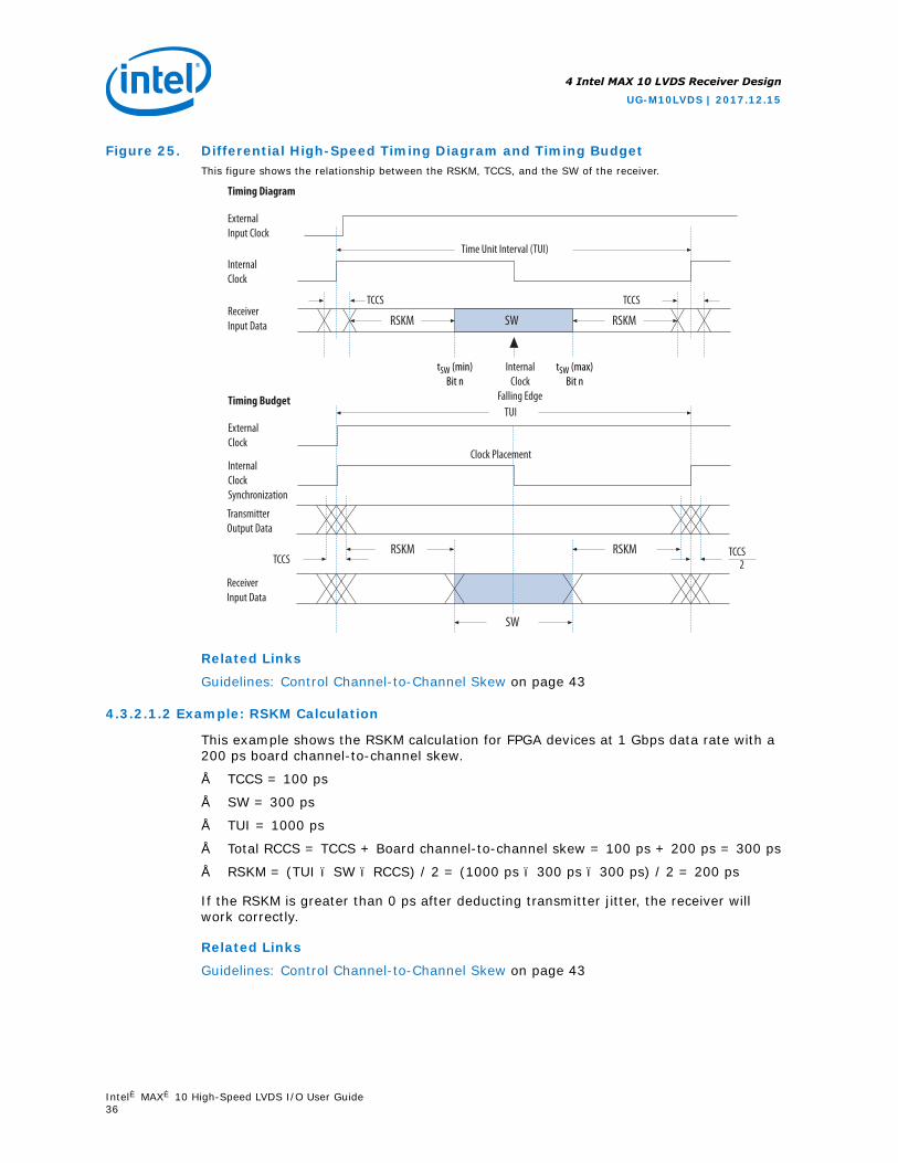
Figure 25. Differential High-Speed Timing Diagram and Timing BudgetThis figure shows the relationship between the RSKM, TCCS, and the SW of the receiver.
TUI
Time Unit Interval (TUI)
TCCS
InternalClock
Falling Edge
tSW (min)Bit n
tSW (max)Bit n
TCCSTCCS
2
ReceiverInput Data
TransmitterOutput Data
InternalClockSynchronization
ExternalClock
ReceiverInput Data
InternalClock
ExternalInput Clock
Timing Budget
Timing Diagram
Clock Placement
SW
TCCS
RSKM RSKM
SW
RSKM RSKM
Related Links
Guidelines: Control Channel-to-Channel Skew on page 43
4.3.2.1.2 Example: RSKM Calculation
This example shows the RSKM calculation for FPGA devices at 1 Gbps data rate with a200 ps board channel-to-channel skew.
• TCCS = 100 ps
• SW = 300 ps
• TUI = 1000 ps
• Total RCCS = TCCS + Board channel-to-channel skew = 100 ps + 200 ps = 300 ps
• RSKM = (TUI – SW – RCCS) / 2 = (1000 ps – 300 ps – 300 ps) / 2 = 200 ps
If the RSKM is greater than 0 ps after deducting transmitter jitter, the receiver willwork correctly.
Related Links
Guidelines: Control Channel-to-Channel Skew on page 43
4 Intel MAX 10 LVDS Receiver Design
UG-M10LVDS | 2017.12.15
Intel® MAX® 10 High-Speed LVDS I/O User Guide36

4.3.2.2 Guidelines: LVDS Receiver Timing Constraints
For receiver designs that uses the core logic to implement the SERDES circuits, youmust set proper timing constraints.
For LVDS receiver data paths where the PLL operation is in source-synchronouscompensation mode, the Intel Quartus Prime compiler automatically ensures that theassociated delay chain settings are set correctly.
However, if the input clock and data at the receiver are not edge- or center-aligned, itmay be necessary for you to set the timing constraints in the Intel Quartus PrimeTiming Analyzer. The timing constraints specify the timing requirements necessary toensure reliable data capture.
Related Links
Timing Constraints, Intel Quartus Prime Standard EditionHandbook Volume 3:Verification
4.3.3 Guidelines: Floating LVDS Input Pins
You can implement floating LVDS input pins in Intel MAX 10 devices.
For floating LVDS input pins, apply a 100 Ω differential resistance across the P and Nlegs of the LVDS receiver. You can use external termination.
If you use floating LVDS input pins, Intel recommends that you use external biasingschemes to reduce noise injection and current consumption.
4.3.4 Guidelines: LVDS Receiver Channels Placement
To maintain an acceptable noise level on the VCCIO supply, observe the placementrestrictions for single-ended I/O pins in relation to differential pads.
Intel recommends that you create a Intel Quartus Prime design, specify your deviceI/O assignments, and compile your design to validate your pin placement. The IntelQuartus Prime software verifies your pin connections against the I/O assignment andplacement rules to ensure that the device will operate properly.
You can use the Intel Quartus Prime Pin Planner Package view to ease differential I/Oassignment planning:
• On the View menu, click Show Differential Pin Pair Connections to highlightthe differential pin pairing. The differential pin pairs are connected with red lines.
• For differential pins, you only need to assign the signal to a positive pin. The IntelQuartus Prime software automatically assigns the negative pin if the positive pin isassigned with a differential I/O standard.
In Intel MAX 10 devices, the routing of each differential pin pair is matched.Consequently, the skew between the positive and the negative pins is minimal. Theinternal routes of both pins in a differential pair are matched even if the pins are non-adjacent.
The Altera Soft LVDS IP core for Intel MAX 10 devices supports a maximum of 18channels per IP instantiation. Each channel can support deserialization factor (paralleldata width) from one to ten bits. When you are grouping channels for an application,you must consider the channel to channel skew during Fitter placement. To minimize
4 Intel MAX 10 LVDS Receiver Design
UG-M10LVDS | 2017.12.15
Intel® MAX® 10 High-Speed LVDS I/O User Guide37

skew, place all LVDS channels in the group side by side. For your PCB design, Intelrecommends that you perform package skew compensation to minimize skew andmaximize performance.
Note: For Intel MAX 10 devices, the Intel Quartus Prime software does not provide apackage skew compensation report.
4.3.5 Guidelines: LVDS Channels PLL Placement
Each PLL in the Intel MAX 10 device can drive only the LVDS channels in I/O banks onthe same edge as the PLL.
Table 10. Examples of Usable PLL to Drive I/O Banks in Intel MAX 10 Devices
I/O Bank Edge Input refclk GCLK mux Usable PLL
Left Left Left Top left or bottom left
Bottom Bottom Bottom Bottom left or bottom right
Right Right Right Top right or bottom right
Top Top Top Top left or top right
4.3.6 Guidelines: LVDS Receiver Logic Placement
The Intel Quartus Prime software automatically optimizes the SERDES logic placementto meet the timing requirements. Therefore, you do not have to perform placementconstraints on the Altera Soft LVDS IP core logic.
To improve the performance of the Intel Quartus Prime Fitter, you can createLogicLock regions in the device floorplan to confine the transmitter SERDES logicplacement.
• The TCCS parameter is guaranteed per datasheet specification to the entire bankof differential I/Os that are located in the same side. This guarantee applies if thetransmitter SERDES logic is placed within the LAB adjacent to the output pins.
• Constrain the transmitter SERDES logic to the LAB adjacent to the data outputpins and clock output pins to improve the TCCS performance.
4.4 LVDS Receiver Debug and Troubleshooting
You can obtain useful information about the LVDS interface performance with board-level verification using the FPGA prototype.
Although the focus of the board-level verification is to verify the FPGA functionality inyour end system, you can take additional steps to examine the margins. Usingoscilloscopes, you can examine the margins to verify the predicted size of the data-valid window, and the setup and hold margins at the I/O interface.
You can also use the Intel SignalTap II Logic Analyzer to perform system levelverification to correlate the system against your design targets.
4 Intel MAX 10 LVDS Receiver Design
UG-M10LVDS | 2017.12.15
Intel® MAX® 10 High-Speed LVDS I/O User Guide38

4.4.1 Perform RTL Simulation Before Hardware Debug
Before you debug on hardware, Intel recommends that you perform an RTLsimulation. Using the RTL simulation, you can check the code functionality beforetesting in real hardware.
For example, you can use the RTL simulation to verify that when you send a trainingpattern from a remote transmitter, the bitslipping mechanism in your LVDS receiverworks.
4.4.2 Geometry-Based and Physics-Based I/O Rules
You need to consider the I/O placement rules related to LVDS. The Intel Quartus Primesoftware generates critical warning or error messages if the I/O placements rules areviolated.
For more information, refer to the related information.
Related Links
Intel MAX 10 General Purpose I/O User Guide
4 Intel MAX 10 LVDS Receiver Design
UG-M10LVDS | 2017.12.15
Intel® MAX® 10 High-Speed LVDS I/O User Guide39

5 Intel MAX 10 LVDS Transmitter and Receiver DesignYou can implement mixed transmitter and receiver applications using the Intel MAX 10LVDS solution. You can use the Altera Soft LVDS IP core to instantiate soft SERDEScircuitry. The soft SERDES circuitry works with the clocks and differential I/O pins tocreate high-speed differential transmitter and receiver circuits.
In a mixed transmitter and receiver implementation, the transmitter and receiver canshare some FPGA resources.
5.1 Transmitter–Receiver Interfacing
You can instantiate the components for the Altera Soft LVDS interfaces by usinginternal or external PLLs.
Figure 26. Typical Altera Soft LVDS Interfaces with Internal PLL
SERDES logicand DDIO
SERDES logicand DDIO
PLL
PLL
LVDS DestinationDevice
LVDS SourceDevice
LVDS Receiver IP Core
LVDS Transmitter IP Core
FPGA Device
CLOCK andDATA
CLOCK andDATA
UG-M10LVDS | 2017.12.15
Intel Corporation. All rights reserved. Intel, the Intel logo, Altera, Arria, Cyclone, Enpirion, MAX, Nios, Quartusand Stratix words and logos are trademarks of Intel Corporation or its subsidiaries in the U.S. and/or othercountries. Intel warrants performance of its FPGA and semiconductor products to current specifications inaccordance with Intel's standard warranty, but reserves the right to make changes to any products and servicesat any time without notice. Intel assumes no responsibility or liability arising out of the application or use of anyinformation, product, or service described herein except as expressly agreed to in writing by Intel. Intelcustomers are advised to obtain the latest version of device specifications before relying on any publishedinformation and before placing orders for products or services.*Other names and brands may be claimed as the property of others.
ISO9001:2008Registered

Figure 27. Typical Altera Soft LVDS Interfaces with External PLL
SERDES logicand DDIO
SERDES logicand DDIO
LVDS DestinationDevice
LVDS SourceDevice
LVDS Receiver IP Core
LVDS Transmitter IP Core
FPGA Device
DATA
DATAPLLIP Core
PLLIP CoreCLOCK
CLOCK
Related Links
• Intel MAX 10 LVDS Transmitter Design on page 16Provides more information about specific features and support of the LVDStransmitters.
• Intel MAX 10 LVDS Receiver Design on page 26Provides more information about specific features and support of the LVDSreceivers.
5.2 LVDS Transmitter and Receiver FPGA Design Implementation
Intel MAX 10 devices use a soft SERDES architecture to support high-speed I/Ointerfaces. The Intel Quartus Prime software creates the SERDES circuits in the corefabric by using the Altera Soft LVDS IP core. To improve the timing performance andsupport the SERDES, Intel MAX 10 devices use the I/O registers and LE registers inthe core fabric.
5.2.1 LVDS Transmitter and Receiver PLL Sharing Implementation
In applications where an LVDS transmitter and receiver are required, you typicallyneed two PLLs—one for each interface. Using the Altera Soft LVDS IP core, you canreduce PLL usage by sharing one PLL between the transmitter and receiver.
• Turn on the Use common PLL(s) for receivers and transmitters option toallow the Intel Quartus Prime compiler to share the same PLL.
• To share a PLL, several PLLs must have the same PLL settings, such as PLLfeedback mode, clock frequency, and phase settings. The LVDS transmitters andreceivers must use the same input clock frequency and reset input.
• If you are sharing a PLL, you can use more counters to enable differentdeserialization factor and data rates for the transmitters and receivers. However,because you are using more PLL counters, the PLL input clock frequency and thePLL counter resolution cause limitations in clocking the transmitters and receivers.
Note: The number of PLLs available differs among Intel MAX 10 packages. Intel recommendsthat you select a Intel MAX 10 device package that provides sufficient number of PLLclockouts for your design.
5 Intel MAX 10 LVDS Transmitter and Receiver Design
UG-M10LVDS | 2017.12.15
Intel® MAX® 10 High-Speed LVDS I/O User Guide41

5.2.2 Initializing the Altera Soft LVDS IP Core
The PLL locks to the reference clock before the Altera Soft LVDS IP core implementsthe SERDES blocks for data transfer.
During device initialization the PLL starts to lock to the reference clock and becomesoperational when it achieves lock during user mode. If the clock reference is notstable, it corrupts the phase shifts of the PLL output clock. This phase shifts corruptioncan cause failure and corrupt data transfer between the high-speed LVDS domain andthe low-speed parallel domain.
To avoid data corruption, follow these steps when initializing the Altera Soft LVDS IPcore:
1. Assert the pll_areset signal for at least 10 ns.
2. After at least 10 ns, deassert the pll_areset signal.
3. Wait until the PLL lock becomes stable.
After the PLL lock port asserts and is stable, the SERDES blocks are ready foroperation.
5.3 LVDS Transmitter and Receiver Debug and Troubleshooting
You can obtain useful information about the LVDS interface performance with board-level verification using the FPGA prototype.
Although the focus of the board-level verification is to verify the FPGA functionality inyour end system, you can take additional steps to examine the margins. Usingoscilloscopes, you can examine the margins to verify the predicted size of the data-valid window, and the setup and hold margins at the I/O interface.
You can also use the Intel SignalTap II Logic Analyzer to perform system levelverification to correlate the system against your design targets.
5.3.1 Perform RTL Simulation Before Hardware Debug
Before you debug on hardware, Intel recommends that you perform an RTLsimulation. Using the RTL simulation, you can check the code functionality beforetesting in real hardware.
For example, you can use the RTL simulation to verify that when you send a trainingpattern from a remote transmitter, the bitslipping mechanism in your LVDS receiverworks.
5.3.2 Geometry-Based and Physics-Based I/O Rules
You need to consider the I/O placement rules related to LVDS. The Intel Quartus Primesoftware generates critical warning or error messages if the I/O placements rules areviolated.
For more information, refer to the related information.
Related Links
Intel MAX 10 General Purpose I/O User Guide
5 Intel MAX 10 LVDS Transmitter and Receiver Design
UG-M10LVDS | 2017.12.15
Intel® MAX® 10 High-Speed LVDS I/O User Guide42

6 Intel MAX 10 High-Speed LVDS Board DesignConsiderations
To achieve optimal performance from the Intel MAX 10 device, you must considercritical issues such as impedance of traces and connectors, differential routing, andtermination techniques.
6.1 Guidelines: Improve Signal Quality
To improve signal quality, follow these board design guidelines:
• Base your board designs on controlled differential impedance. Calculate andcompare all parameters such as trace width, trace thickness, and the distancebetween two differential traces.
• Maintain equal distance between traces in differential I/O standard pairs as muchas possible. Routing the pair of traces close to each other maximizes the common-mode rejection ratio (CMRR).
• Keep the traces as short as possible to limit signal integrity issues. Longer traceshave more inductance and capacitance.
• Place termination resistors as close to receiver input pins as possible.
• Use surface mount components.
• Avoid 90° corners on board traces.
• Use high-performance connectors.
• Design backplane and card traces so that trace impedance matches the impedanceof the connector and termination.
• Keep an equal number of vias for both signal traces.
• Create equal trace lengths to avoid skew between signals. Unequal trace lengthsresult in misplaced crossing points and decrease system margins as thetransmitter-channel-to-channel skew (TCCS) value increases.
• Limit vias because they cause discontinuities.
• Keep toggling single-ended I/O signals away from differential signals to avoidpossible noise coupling.
• Do not route single-ended I/O clock signals to layers adjacent to differentialsignals.
• Analyze system-level signals.
6.2 Guidelines: Control Channel-to-Channel Skew
For the Intel MAX 10 devices, perform PCB trace compensation to adjust the tracelength of each LVDS channel. Adjusting the trace length improves the channel-to-channel skew when interfacing with receivers.
UG-M10LVDS | 2017.12.15
Intel Corporation. All rights reserved. Intel, the Intel logo, Altera, Arria, Cyclone, Enpirion, MAX, Nios, Quartusand Stratix words and logos are trademarks of Intel Corporation or its subsidiaries in the U.S. and/or othercountries. Intel warrants performance of its FPGA and semiconductor products to current specifications inaccordance with Intel's standard warranty, but reserves the right to make changes to any products and servicesat any time without notice. Intel assumes no responsibility or liability arising out of the application or use of anyinformation, product, or service described herein except as expressly agreed to in writing by Intel. Intelcustomers are advised to obtain the latest version of device specifications before relying on any publishedinformation and before placing orders for products or services.*Other names and brands may be claimed as the property of others.
ISO9001:2008Registered

At the package level, you must control the LVDS I/O skew for each I/O bank and eachside of the device. If you plan to vertically migrate from one device to another usingthe same board design, you must control the package migration skew for eachmigratable LVDS I/O pin.
For information about controlling the LVDS I/O and package skew, refer to the relatedinformation.
Related Links
• Receiver Input Skew Margin on page 34
• RSKM Equation on page 34Explains the relationship between the RSKM, TCCS, and SW.
• Example: RSKM Calculation on page 36
6.3 Guidelines: Determine Board Design Constraints
After you have closed timing for your FPGA design, examine your board design todetermine the different factors that can impact signal integrity. These factors affectoverall timing at the receiving device in the LVDS interface.
The time margin for the LVDS receiver (indicated by the RSKM value) is the timingbudget allocation for board level effects such as:
• Skew—these factors cause board-level skew:
— Board trace lengths
— Connectors usage
— Parasitic circuits variations
• Jitter—jitter effects are derived from factors such as crosstalk.
• Noise—on board resources with imperfect power supplies and reference planesmay also cause noise.
To ensure successful operation of the Altera Soft LVDS IP core receiver, do not exceedthe timing budget.
Related Links
Board Design Guidelines Solution CenterProvides resources related to board design for Intel devices.
6.4 Guidelines: Perform Board Level Simulations
After you determined the system requirements and finalized the board designconstraints, use an electronic design automation (EDA) simulation tool to performboard-level simulations. Use the IBIS or HSPICE models of the FPGA and the targetLVDS device for the simulation.
The board-level simulation ensures optimum board setup where you can determine ifthe data window conforms to the input specification (electrical and timing) of the LVDSreceiver.
6 Intel MAX 10 High-Speed LVDS Board Design Considerations
UG-M10LVDS | 2017.12.15
Intel® MAX® 10 High-Speed LVDS I/O User Guide44

You can use the programmable pre-emphasis feature on the true LVDS output buffers,for example, to compensate for the frequency-dependent attenuation of thetransmission line. With this feature, you can maximize the data eye opening at the farend receiver especially on long transmission lines.
Related Links
• Intel IBIS ModelsProvides IBIS models of Intel devices for download.
• Intel HSPICE ModelsProvides SPICE models of Intel devices for download.
• IBIS Model GenerationProvides video that demonstrates how to generate IBIS file using the IntelQuartus Prime software.
6 Intel MAX 10 High-Speed LVDS Board Design Considerations
UG-M10LVDS | 2017.12.15
Intel® MAX® 10 High-Speed LVDS I/O User Guide45

7 Altera Soft LVDS IP Core ReferencesYou can set various parameter settings for the Altera Soft LVDS IP core to customizeits behaviors, ports, and signals.
The Intel Quartus Prime software generates your customized Altera Soft LVDS IP coreaccording to the parameter options that you set in the parameter editor.
7.1 Altera Soft LVDS Parameter Settings
There are four groups of options: General , PLL Settings , Receiver Settings , andTransmitter Settings
Table 11. Altera Soft LVDS Parameters - General
Parameter Condition AllowedValues
Description
Power Supply Mode — • Dual Supply• Single
Supply
Specifies whether the target device is a single ordual supply device.
Functional mode — • RX• TX
Specifies the functional mode for the Altera SoftLVDS IP core:• RX—specifies the IP is an LVDS receiver.• TX—specifies the IP is an LVDS transmitter.
Number of channels — 1–18 Specifies the number of LVDS channels.
SERDES factor — 1, 2, 4, 5, 6, 7,8, 9, 10
Specifies the number of bits per channel.
Table 12. Altera Soft LVDS Parameters - PLL Settings
Parameter Condition AllowedValues
Description
Use external PLL Not applicable for x1and x2 modes.
• On• Off
Specifies whether the Altera Soft LVDS IP coregenerates a PLL or connects to a user-specifiedPLL.
Data rate — Refer to thedevicedatasheet.
Specifies the data rate going out of the PLL. Themultiplication value for the PLL isOUTPUT_DATA_RATE divided by INCLOCK_PERIOD.
Inclock frequency — Depends onData rate.
Specifies the input clock frequency to the PLL inMHz.
Enable rx_locked port • General, Functionalmode = RX
• Use external PLL =Off
• On• Off
If turned on, enables the rx_locked port.
continued...
UG-M10LVDS | 2017.12.15
Intel Corporation. All rights reserved. Intel, the Intel logo, Altera, Arria, Cyclone, Enpirion, MAX, Nios, Quartusand Stratix words and logos are trademarks of Intel Corporation or its subsidiaries in the U.S. and/or othercountries. Intel warrants performance of its FPGA and semiconductor products to current specifications inaccordance with Intel's standard warranty, but reserves the right to make changes to any products and servicesat any time without notice. Intel assumes no responsibility or liability arising out of the application or use of anyinformation, product, or service described herein except as expressly agreed to in writing by Intel. Intelcustomers are advised to obtain the latest version of device specifications before relying on any publishedinformation and before placing orders for products or services.*Other names and brands may be claimed as the property of others.
ISO9001:2008Registered

Parameter Condition AllowedValues
Description
Enable tx_locked port • General, Functionalmode = TX
• Use external PLL =Off
• On• Off
If turned on, enables the tx_locked port.
Enable pll_areset port Use external PLL = Off • On• Off
If turned on, enables the pll_areset port ininternal PLL mode.In external PLL mode, the pll_areset port is notavailable.
Enable tx_data_resetport
• General, Functionalmode = TX
• Use external PLL =On
• On• Off
If turned on, enables the tx_data_reset port.
Enable rx_data_resetport
• General, Functionalmode = RX
• Use external PLL =On
• On• Off
If turned on, enables the rx_data_reset port.
Use common PLL(s) forreceivers andtransmitters
Use external PLL = Off • On• Off
• On—specifies that the compiler uses the samePLL for the LVDS receiver and transmitter.
• Off—specifies that the compiler uses differentPLLs for LVDS receivers and transmitters.
You can use common PLLs if you use the sameinput clock source, deserialization factor,pll_areset source, and data rates.
Enable self-reset on losslock in PLL
Use external PLL = Off • On• Off
If turned on, the PLL is reset when it loses lock.
Desired transmitterinclock phase shift
• General, Functionalmode = TX
• Use external PLL =Off
Depends onData rate.
Specifies the phase shift parameter used by thePLL for the transmitter.
Desired receiver inclockphase shift
• General, Functionalmode = RX
• Use external PLL =Off
Depends onData rate.
Specifies the phase shift parameter used by thePLL for the receiver.
Table 13. Altera Soft LVDS Parameters - Receiver Settings
Parameter Condition AllowedValues
Description
Enable bitslip mode General, Functionalmode = RX
• On• Off
If turned on, enables the rx_data_align port.
Enable independentbitslip controls for eachchannel
General, Functionalmode = RX
• On• Off
If turned on, enables therx_channel_data_align port.The rx_channel_data_align is an edge-sensitive bit slip control signal:• Each rising edge on this signal causes the data
realignment circuitry to shift the word boundaryby one bit.
• The minimum pulse width requirement is oneparallel clock cycle.
continued...
7 Altera Soft LVDS IP Core References
UG-M10LVDS | 2017.12.15
Intel® MAX® 10 High-Speed LVDS I/O User Guide47

Parameter Condition AllowedValues
Description
Enablerx_data_align_resetport
• General, Functionalmode = RX
• Enable bitslip mode= On
• Enable independentbitslip controls foreach channel = Off
• On• Off
If turned on, enables the rx_data_align_resetport.
Add extra register forrx_data_align port
• General, Functionalmode = RX
• Enable bitslip mode= On
• On• Off
If turned on, registers the rx_data_align port.If you turn this option off, you must pre-registerthe rx_data_align[] port in the logic that feedsthe receiver.
Bitslip rollover value • General, Functionalmode = RX
• Enable bitslip mode= On
1–11 Specifies the number of pulses before the circuitryrestores the serial data latency to 0.
Use RAM buffer — • On• Off
If turned on, the Altera Soft LVDS IP coreimplements the output synchronization buffer inthe embedded memory blocks.This implementation option uses more logic thanUse a multiplexer and synchronizationregister option but results in the correct wordalignment.
Use a multiplexer andsynchronization register
— • On• Off
If turned on, the Altera Soft LVDS IP coreimplements a multiplexer instead of a buffer foroutput synchronization.
Use logic element basedRAM
— • On• Off
If turned on, the Altera Soft LVDS IP coreimplements the output synchronization buffer inthe logic elements.This implementation option uses more logic thanUse a multiplexer and synchronizationregister option but results in the correct wordalignment.
Register outputs General, Functionalmode = RX
• On• Off
If turned on, registers the rx_out[] port.If you turn this option off, you must pre-registerthe rx_out[] port in the logic that feeds thereceiver.
Table 14. Altera Soft LVDS Parameters - Transmitter Settings
Parameter Condition AllowedValues
Description
Enable 'tx_outclock'output port
• General, Functionalmode = TX
• PLL Settings, Useexternal PLL = Off
• On• Off
If turned on, enables the tx_outclock port.
continued...
7 Altera Soft LVDS IP Core References
UG-M10LVDS | 2017.12.15
Intel® MAX® 10 High-Speed LVDS I/O User Guide48

Parameter Condition AllowedValues
Description
Every tx_outclock signal goes through the shiftregister logic, except in the following parameterconfigurations:• When the outclock_divide_by signal = 1• When the outclock_divide_by signal is
equal to the deserialization_factorsignal (for odd factors only), and theoutclock_duty_cycle signal is 50
Tx_outclock divisionfactor
• General, Functionalmode = TX
• PLL Settings, Useexternal PLL = Off
• Enable 'tx_outclock'output port = On
Depends onSERDESfactor.
Specifies that the frequency of the tx_outclocksignal is equal to the the transmitter output datarate divided by the selected division factor.
Outclock duty cycle • General, Functionalmode = TX
• PLL Settings, Useexternal PLL = Off
• Enable 'tx_outclock'output port = On
Depends onSERDESfactor andTx_outclockdivisionfactor.
Specifies the external clock timing constraints.
Desired transmitteroutclock phase shift
• General, Functionalmode = TX
• PLL Settings, Useexternal PLL = Off
• Enable 'tx_outclock'output port = On
Depends onData rate.
Specifies the phase shift of the output clockrelative to the input clock.
Register 'tx_in' inputport
General, Functionalmode = TX
• On• Off
If turned on, registers the tx_in[] port.If you turn this option off, you must pre-registerthe tx_in[] port in the logic that feeds thetransmitter.
Clock resource • General, Functionalmode = TX
• Register 'tx_in' inputport = On
• tx_inclock• tx_corecloc
k
Specifies which clock resource registers the tx_ininput port.
Enable 'tx_coreclock'output port
General, Functionalmode = TX
• On• Off
If turned on, enables the tx_coreclock outputport.
Clock source for'tx_coreclock'
• General, Functionalmode = TX
• Enable 'tx_coreclock'output port = On
• Autoselection
• Global clock• Regional
clock• Dual-
Regionalclock
Specifies which clock resource drives thetx_coreclock output port.
Related Links
• Altera Soft LVDS IP Core in Transmitter Mode on page 20
• Altera Soft LVDS IP Core in Receiver Mode on page 31
7.2 Altera Soft LVDS Interface Signals
Depending on parameter settings you specify, different signals are available for theAltera Soft LVDS IP core.
7 Altera Soft LVDS IP Core References
UG-M10LVDS | 2017.12.15
Intel® MAX® 10 High-Speed LVDS I/O User Guide49

Table 15. Transmitter Interface Signals
Signal Name Direction Width (Bit) Description
pll_areset Input 1 Asynchronously resets all counters to the initialvalues.
tx_data_reset
Input <n>
Asynchronous reset for the shift registers, captureregisters, and synchronization registers for allchannels.• This signal is used if Use external PLL
parameter setting is turned on.• This signal does not affect the data realignment
block or the PLL.
tx_in[]
Input <m>
This signal is parallel data that Altera Soft LVDS IPcore transmits serially.Input data is synchronous to the tx_coreclocksignal. The data bus width per channel is the sameas the serialization factor (SF).
tx_inclock
Input 1
Reference clock input for the transmitter PLL.The parameter editor automatically selects theappropriate PLL multiplication factor based on thedata and reference clock frequency.
tx_coreclock
Output 1
Output clock that feeds non-peripheral logic.FPGA fabric–transmitter interface clock—theparallel transmitter data generated in the FPGAfabric is clocked with this clock.
tx_locked
Output 1
Provides the LVDS PLL status:• Remains high when the PLL is locked to the
input reference clock.• Remains low when the PLL fails to lock.
tx_out[]
Output <n>
Serialized LVDS data output signal of <n>channels.tx_out[(<n>-1)..0] drives parallel data fromtx_in[(<J> × <n>)-1 ..0] where <J> is theserialization factor and <n> is the number ofchannels. tx_out[0] drives data fromtx_in[(<J>-1)..0]. tx_out[1] drives datafrom the next <J> number of bits on tx_in.
tx_outclockOutput 1
External reference clock.The frequency of this clock is programmable to bethe same as the data rate.
Table 16. Receiver Interface Signals
signal Name Direction Width (Bit) Description
rx_data_reset Input <n> Asynchronous reset for all channels, excluding thePLL.• This signal is available if Use external PLL
parameter setting is turned on.• You must externally synchronize this signal with
the fast clock.
rx_in[] Input <n> LVDS serial data input signal of <n> channels.rx_in[(<n>-1)..0] is deserialized and drivenon rx_out[(<J> × <n>)-1 ..0] where <J> isthe deserialization factor and <n> is the number of
continued...
7 Altera Soft LVDS IP Core References
UG-M10LVDS | 2017.12.15
Intel® MAX® 10 High-Speed LVDS I/O User Guide50

signal Name Direction Width (Bit) Description
channels. rx_in[0] drives data torx_out[(<J>-1)..0]. rx_in[1] drives data tothe next <J> number of bits on rx_out.
rx_inclock Input 1 LVDS reference input clock.The parameter editor automatically selects theappropriate PLL multiplication factor based on thedata rate and reference clock frequency selection.
rx_coreclk Input <n> LVDS reference input clock.• Replaces the non-peripheral clock from the PLL.• One clock for each channel.
rx_locked Output 1 Provides the LVDS PLL status:• Stays high when the PLL is locked to the input
reference clock.• Stays low when the PLL fails to lock.
rx_out Output <m> Receiver parallel data output.The data bus width per channel is the same as thedeserialization factor (DF).
rx_outclock Output 1 Parallel output clock from the receiver PLL.• This signal is not available if you turn on the
Use external PLL parameter setting.• The FPGA fabric–receiver interface clock must
be driven by the PLL instantiated through theALTPLL parameter editor.
rx_data_align Input 1 Controls the byte alignment circuitry.You can register this signal using therx_outclock signal.
rx_data_align_reset Input 1 Resets the byte alignment circuitry.Use the rx_data_align_reset input signal if:• You need to reset the PLL during device
operation.• You need to re-establish the word alignment.
rx_channel_data_align Input <n> Controls byte alignment circuitry.
rx_cda_reset Input <n> Asynchronous reset to the data realignmentcircuitry. This signal resets the data realignmentblock.The minimum pulse width requirement for thisreset is one parallel clock cycle.
7 Altera Soft LVDS IP Core References
UG-M10LVDS | 2017.12.15
Intel® MAX® 10 High-Speed LVDS I/O User Guide51

8 Intel MAX 10 High-Speed LVDS I/O User Guide ArchivesIf an IP core version is not listed, the user guide for the previous IP core version applies.
IP Core Version User Guide
16.1 MAX 10 High-Speed LVDS I/O User Guide
16.0 MAX 10 High-Speed LVDS I/O User Guide
15.1 MAX 10 High-Speed LVDS I/O User Guide
15.0 MAX 10 High-Speed LVDS I/O User Guide
14.1 MAX 10 High-Speed LVDS I/O User Guide
UG-M10LVDS | 2017.12.15
Intel Corporation. All rights reserved. Intel, the Intel logo, Altera, Arria, Cyclone, Enpirion, MAX, Nios, Quartusand Stratix words and logos are trademarks of Intel Corporation or its subsidiaries in the U.S. and/or othercountries. Intel warrants performance of its FPGA and semiconductor products to current specifications inaccordance with Intel's standard warranty, but reserves the right to make changes to any products and servicesat any time without notice. Intel assumes no responsibility or liability arising out of the application or use of anyinformation, product, or service described herein except as expressly agreed to in writing by Intel. Intelcustomers are advised to obtain the latest version of device specifications before relying on any publishedinformation and before placing orders for products or services.*Other names and brands may be claimed as the property of others.
ISO9001:2008Registered

9 Document Revision History for Intel MAX 10 High-SpeedLVDS I/O User Guide
Date Version Changes
December 2017 2017.12.15 • Added short descriptions about the true and emulated LVDS buffers.• Added single power supply U324 package.• Updated the topic about using the Altera Soft LVDS IP core (receiver) in
external PLL mode to remove the ALTPLL IP core slow clock output (c1)connection to the Altera Soft LVDS rx_synclock input for evendeserialization factor. The rx_synclock is not used by the Altera SoftLVDS IP core when the deserialization factor is even.
• Updated the section about high-speed I/O timing budget:— Updated the high-speed I/O timing budget topic to clarify that Intel
MAX 10 devices implements SERDES in LEs.— Removed information about obtaining RSKM report in the Intel
Quartus Prime software. The software does not support generatingRSKM report for Intel MAX 10 devices.
— Removed the topic about assigning input delay to the LVDS receiver.— Added link to timing constraints section of the Intel Quartus Prime
Standard Edition Handbook Volume 3: Verification.• Updated the condition and description for the Enable pll_areset port
parameter to specify that it is not available in external PLL mode.• Throughout the document, added links to related information to
improve usability.• Further edits for Intel rebranding.
February 2017 2017.02.21 Rebranded as Intel.
October 2016 2016.10.31 • Added related information links in the topic about LVDS channelssupport.
• Restructured and updated the topic about the RSKM.• Added a topic that describes how to assign input delay to the LVDS
receiver using the TimeQuest Timing Analyzer.
May 2016 2016.05.02 • Added true RSDS and emulated RSDS (three resistors) transmittersupport for single supply Intel MAX 10 devices.
• Updated the transmitter and receiver channels placement topics todescribe about minimizing skew when you group LVDS channels for anapplication.
• Updated the description of the rx_data_reset interface signal tospecify that you must externally synchronize it with the fast clock.
• Updated the General tab of the Altera Soft LVDS parameter settings:— Added the Power Supply Mode option.— Updated the allowed values of the SERDES factor parameter.
continued...
UG-M10LVDS | 2017.12.15
Intel Corporation. All rights reserved. Intel, the Intel logo, Altera, Arria, Cyclone, Enpirion, MAX, Nios, Quartusand Stratix words and logos are trademarks of Intel Corporation or its subsidiaries in the U.S. and/or othercountries. Intel warrants performance of its FPGA and semiconductor products to current specifications inaccordance with Intel's standard warranty, but reserves the right to make changes to any products and servicesat any time without notice. Intel assumes no responsibility or liability arising out of the application or use of anyinformation, product, or service described herein except as expressly agreed to in writing by Intel. Intelcustomers are advised to obtain the latest version of device specifications before relying on any publishedinformation and before placing orders for products or services.*Other names and brands may be claimed as the property of others.
ISO9001:2008Registered

Date Version Changes
November 2015 2015.11.02 • Updated the high-speed LVDS circuitry figure to correct the flow fromC1 in ALTPLL to inclock of ALTERA_SOFT_LVDS. Previously, the figureshows a bidirectional flow.
• Updated the steps for determining the external PLL clock parametersfor the receiver to clarify the clock names listed by the Intel QuartusPrime compilation report.
• Updated the topic about Altera Soft LVDS parameter settings:— Added links to topics about PLL and high-speed I/O performance in
the device datasheet.— Corrected the conditions required to use the Enable
tx_data_reset port and Enable rx_data_reset port parameters.You must turn on the Use external PLL option first.
— Updated the allowed values for the Tx_outclock division factorand Outclock duty cycle parameters.
— Updated the condition for the Desired transmitter outclockphase shift parameter.
• Removed the topics about generating IP cores and the files generatedby the IP core, and added a link to Introduction to Altera IP Cores.
• Removed the statement about getting TCCS value from the IntelQuartus Prime compilation report. You can get TCCS value from thedevice datasheet.
• Added guidelines topic about enabling LVDS pre-emphasis for Intel MAX10 devices in the E144 package.
• Updated the guidelines to control channel-to-channel skew to removestatements about getting the trace delay amount from the Fitter Reportpanel.
• Added link to video that demonstrates how to generate IBIS file usingthe Intel Quartus Prime software.
• Changed instances of Quartus II to Quartus Prime.
continued...
9 Document Revision History for Intel MAX 10 High-Speed LVDS I/O User Guide
UG-M10LVDS | 2017.12.15
Intel® MAX® 10 High-Speed LVDS I/O User Guide54

Date Version Changes
May 2015 2015.05.04 • Removed the F672 package from the 10M25 device.• Updated the number of bottom true receiver channels for package
M153 of the 10M02 device from 49 to 13.• Added BLVDS output support in single-supply Intel MAX 10 devices.
Previously, BLVDS support for single-supply devices was input only.• Updated the RSKM definition in the topic about receiver input skew
margin to include jitter induced from core noise and I/O switchingnoise.
• Updated topics related to using the Altera Soft LVDS IP core(transmitter or receiver) in external PLL mode:— Added rx_readclock, rx_syncclock, and tx_synclock ports.— Removed pll_areset port.— Added examples for odd and even serialization factors.— Added procedures to obtain the external PLL clock parameters.— Removed similar guidelines in the chapter for the transmitter and
receiver design. The updated guidelines for the receiver only andtransmitter only designs can apply for designs that use bothtransmitters and receivers.
• Updated parameter settings of the Altera Soft LVDS IP core:— Removed allowed values "6" and "9" from the SERDES factor
parameter.— Added allowed value "Off" to the Enable pll_areset port
parameter.— Updated the parameter label Register_rx_bitslip_ctrl port to
Add extra register for rx_data_align port and specified that youmust pre-register the port if you turn it on.
December 2014 2014.12.15 • Updated table listing LVDS channels to include LVDS channel counts foreach device package.
• Added information in the topics about channels placement that IntelMAX 10 devices support x18 bundling mode.
• Updated the examples in topics about channels PLL placement toprovide more details.
• Added link to the MAX 10 Clocking and PLL User Guide that providesmore information about the PLL and the PLL output counters used toclock the soft SERDES.
September 2014 2014.09.22 Initial release.
9 Document Revision History for Intel MAX 10 High-Speed LVDS I/O User Guide
UG-M10LVDS | 2017.12.15
Intel® MAX® 10 High-Speed LVDS I/O User Guide55