Embed Size (px)
Citation preview

Document Number: 326777-015
Intel® 7 Series / C216 Chipset Family Platform Controller Hub (PCH) FamilySpecification Update
May 2014
Revision 015

2 Specification Update
By using this document, in addition to any agreements you have with Intel, you accept the terms set forth below.
You may not use or facilitate the use of this document in connection with any infringement or other legal analysis concerning Intel products described herein. You agree to grant Intel a non-exclusive, royalty-free license to any patent claim thereafter drafted which includes subject matter disclosed herein.
INFORMATION IN THIS DOCUMENT IS PROVIDED IN CONNECTION WITH INTEL PRODUCTS. NO LICENSE, EXPRESS OR IMPLIED, BY ESTOPPEL OR OTHERWISE, TO ANY INTELLECTUAL PROPERTY RIGHTS IS GRANTED BY THIS DOCUMENT. EXCEPT AS PROVIDED IN INTEL'S TERMS AND CONDITIONS OF SALE FOR SUCH PRODUCTS, INTEL ASSUMES NO LIABILITY WHATSOEVER AND INTEL DISCLAIMS ANY EXPRESS OR IMPLIED WARRANTY, RELATING TO SALE AND/OR USE OF INTEL PRODUCTS INCLUDING LIABILITY OR WARRANTIES RELATING TO FITNESS FOR A PARTICULAR PURPOSE, MERCHANTABILITY, OR INFRINGEMENT OF ANY PATENT, COPYRIGHT OR OTHER INTELLECTUAL PROPERTY RIGHT.
A "Mission Critical Application" is any application in which failure of the Intel Product could result, directly or indirectly, in personal injury or death. SHOULD YOU PURCHASE OR USE INTEL'S PRODUCTS FOR ANY SUCH MISSION CRITICAL APPLICATION, YOU SHALL INDEMNIFY AND HOLD INTEL AND ITS SUBSIDIARIES, SUBCONTRACTORS AND AFFILIATES, AND THE DIRECTORS, OFFICERS, AND EMPLOYEES OF EACH, HARMLESS AGAINST ALL CLAIMS COSTS, DAMAGES, AND EXPENSES AND REASONABLE ATTORNEYS' FEES ARISING OUT OF, DIRECTLY OR INDIRECTLY, ANY CLAIM OF PRODUCT LIABILITY, PERSONAL INJURY, OR DEATH ARISING IN ANY WAY OUT OF SUCH MISSION CRITICAL APPLICATION, WHETHER OR NOT INTEL OR ITS SUBCONTRACTOR WAS NEGLIGENT IN THE DESIGN, MANUFACTURE, OR WARNING OF THE INTEL PRODUCT OR ANY OF ITS PARTS.
Intel may make changes to specifications and product descriptions at any time, without notice. Designers must not rely on the absence or characteristics of any features or instructions marked "reserved" or "undefined". Intel reserves these for future definition and shall have no responsibility whatsoever for conflicts or incompatibilities arising from future changes to them. The information here is subject to change without notice. Do not finalize a design with this information.
The products described in this document may contain design defects or errors known as errata which may cause the product to deviate from published specifications. Current characterized errata are available on request.
Contact your local Intel sales office or your distributor to obtain the latest specifications and before placing your product order.
Copies of documents which have an order number and are referenced in this document, or other Intel literature, may be obtained by calling 1-800-548-4725, or go to: http://www.intel.com/design/literature.htm
Intel® High Definition Audio (Intel® HD Audio): Requires an Intel® HD Audio enabled system. Consult your PC manufacturer for more information. Sound quality will depend on equipment and actual implementation. For more information about Intel® HD Audio, refer to http://www.intel.com/design/chipsets/hdaudio.htm
Intel® Active Management Technology (Intel® AMT) requires activation and a system with a corporate network connection, an Intel® AMT-enabled chipset, network hardware and software. For notebooks, Intel AMT may be unavailable or limited over a host OS-based VPN, when connecting wirelessly, on battery power, sleeping, hibernating or powered off. Results dependent upon hardware, setup & configuration. For more information, visit http://www.intel.com/technology/platform-technology/intel-amt Intel® Virtualization Technology (Intel® VT) for Directed I/O (Intel® VT-d) requires a computer system with an enabled Intel® processor, BIOS, virtual machine monitor (VMM). Functionality, performance or other benefits will vary depending on hardware and software configurations. Software applications may not be compatible with all operating systems. Consult your PC manufacturer. For more information, visit http://www.intel.com/go/ virtualization
I2C is a two-wire communications bus/protocol developed by NXP. SMBus is a subset of the I2C bus/protocol and was developed by Intel. Implementations of the I2C bus/protocol may require licenses from various entities, including NXP Semiconductors N.V.Contact your local Intel sales office or your distributor to obtain the latest specifications and before placing your product order.
Intel, Intel Core, Intel AMT, and the Intel logo are trademarks of Intel Corporation in the U.S. and other countries.
*Other names and brands may be claimed as the property of others.
Copyright © 2012-2014, Intel Corporation. All rights reserved.

Specification Update 3
Contents
Revision History ........................................................................................................4
Preface ......................................................................................................................7
Summary Tables of Changes ......................................................................................8
Identification Information .......................................................................................11
PCH Device and Revision Identification ...................................................................12
Errata ......................................................................................................................15
Specification Changes..............................................................................................23
Specification Clarifications ......................................................................................25
Documentation Changes ..........................................................................................29
§ §§

Revision History
4 Specification Update
Revision History
Revision Description Date
001 Initial Release April 2012
002
• Added— Errata: 1: USB Isoch In Transfer Error Issue, 2: USB Babble Detected with SW
Overscheduling, 3: USB Full-/low-speed EOP Issue, 4: USB PLL Control FSM Not Getting Reset on Global Reset, 5: Asynchronous Retries Prioritized Over Periodic Transfers, 6: USB FS/LS Incorrect Number of Retries, 7: SATA Signal Voltage Level Violation, 8: SATA Differential Return Loss Violations, 9: High-speed USB 2.0 Transmit Signal Amplitude, 10: Delayed Periodic Traffic Timeout Issue, 11: USB Full-/Low-speed Port Reset or Clear TT Buffer Request, 12: Intel® AMT and Intel® Standard Manageability KT/SOL Interrupt Status Cleared Prematurely, 13: xHC Data Packet Header and Payload Mismatch Error Condition, 14: USB SuperSpeed Packet with Invalid Type Field Issue, 15: xHC Behavior with Three Consecutive Failed U3 Entry Attempts, and 16: Incorrect IRQ(x) Vector Returned for 8259 Interrupts With RAEOI Enabled.
April 2012
003 • Updated document for typographical errors. Change bars are based off of deltas from Revision 001. May 2012
004
• Updated— Markings.— PCH Device and Revision Identification.— Errata updated to include Intel® C216 Chipset.
May 2012
005• Added
— Errata: 17: USB RMH False Disconnect Issue and 18: xHCI Transaction for Unplugged Device Not Retired and 18: xHCI Transaction for Unplugged Device Not Retired.
May 2012
006
• Updated— Markings table to add Intel® Q77 Express Chipset, Intel® Q75 Express Chipset, Mobile
Intel® QM77 Express Chipset, and Mobile Intel® QS77 Express Chipset.— PCH Device and Revision Identification to add Intel® Q77 Express Chipset, Intel® Q75
Express Chipset, Mobile Intel® QM77 Express Chipset, and Mobile Intel® QS77 Express Chipset.
June 2012
007
• Updated— Replaced Errata 17 and 18 inadvertently not included in Revision 006.
• Added— Errata: 19: USB RMH Think Time Issue, 20: USB 3.0 Device Issues When Connected
During Sx, 21: USB 3.0 Tx De-Emphasis Violations, and 22: Max Packet Size and Transfer Descriptor Length Mismatch.
— Documentation Changes: 1: Integrated Digital Display Audio Revision ID Correction, 2: t200a Correction, 3: Function Level Reset Pending Status Register Correction, and 4: Miscellaneous Documentation Correction.
June 2012
008
• Updated— Markings table to add Mobile Intel® NM70 Express Chipset.— PCH Device and Revision Identification to add Mobile Intel® NM70 Express Chipset
and correct LPC Device ID for Mobile Intel® QS77 Express Chipset.• Added
— Specification Change: 1: Addition of Mobile Intel® NM70 Express Chipset.
July 2012
009
• Updated— PCH Device and Revision Identification.
• Added— Erratum: 23: USB Full-/low-speed Device Removal Issue.— Specification Clarifications: 1: RAID 1 Description, 2: V_PROC_IO Definition, 3:
Manageability Signals Clarifications, and 4: ACPRESENT/GPIO31 Definition.— Documentation Change: 5: SPI Required Region Correction.
July 2012

Revision History
Specification Update 5
§ §
010
• Updated— Mobile Intel® NM70 Express Chipset naming.
• Added— Erratum: 24: Packet Loss on Intel® 82579 Gigabit Ethernet Controller.— Specification Clarification: 5: SPI Overview— Documentation Changes: 6: High Precision Event Timers Functional Description and
7: Miscellaneous Documentation Corrections II.
August 2012
011
Added• Erratum: Intel® 7 / C216 Series Chipset Family xHCI FS/LS Issue with Delayed Split
Transactions.• Documentation Changes: Mobile Intel® 7 Series Chipset Family SKUs Update.
Removed• Specification Change: 1. b. Table 1-5 addition.
Note: NM70 addition had combined to Table 1-3 in Document Changes #8.
March 2013
012
Added• Erratum: 26- Intel® 7 / C216 Series Chipset Family PCI-Express Root Ports Unsupported
Request Complete Issue; 27- Intel® 7 / C216 Series Chipset Family SATA Automatic Partial Slumber Transitions Issue; 28- Intel® 7 / C216 Series Chipset Family - High-Speed USB devices may enumerate as Full-Speed connected to xHCI port.
June 2013
013Added• 29 - RMH port disabled due to Device Initiated Remote Wake• 30 - Enumeration Issue when Resuming for Sx.
November 2013
014Added• 31 - Clearing xHCI PME_EN May Not Disable USB 2.0 Wake Events
April 2014
015Added• 32 - xHCI Controller May Delayed Transactions Due to Short Packets Issue
May 2014
Revision Description Date

Revision History
6 Specification Update

Preface
Specification Update 7
Preface
This document is an update to the specifications contained in the Affected Documents/Related Documents table below. This document is a compilation of device and documentation errata, specification clarifications and changes. It is intended for hardware system manufacturers and software developers of applications, operating systems, or tools.
Information types defined in Nomenclature are consolidated into the specification update and are no longer published in other documents.
This document may also contain information that was not previously published.
Affected Documents/Related Documents
NomenclatureErrata are design defects or errors. Errata may cause the behavior of the PCH to deviate from published specifications. Hardware and software designed to be used with any given stepping must assume that all errata documented for that stepping are present in all devices.
Specification Changes are modifications to the current published specifications. These changes will be incorporated in any new release of the specification.
Specification Clarifications describe a specification in greater detail or further highlight a specification’s impact to a complex design situation. These clarifications will be incorporated in any new release of the specification.
Documentation Changes include typos, errors, or omissions from the current published specifications. These will be incorporated in any new release of the specification.
§ §
Title Document Number
Intel® 7 Series / C216 Chipset Family Platform Controller Hub (PCH) Datasheet 326776-003

Summary Tables of Changes
8 Specification Update
Summary Tables of Changes
The following tables indicate the errata, specification changes, specification clarifications, or documentation changes which apply to the product. Intel may fix some of the errata in a future stepping of the component and account for the other outstanding issues through documentation or specification changes as noted. These tables use the following notations:
Codes Used in Summary Tables
SteppingX: Erratum exists in the stepping indicated. Specification Change
that applies to the stepping indicated.
(No mark)
or (Blank box): This erratum is fixed or not applicable in listed stepping or Specification Change does not apply to listed stepping.
StatusDoc: Document change or update will be implemented.
Plan Fix: This erratum may be fixed in a future stepping of the product.
Fixed: This erratum has been previously fixed.
No Fix: There are no plans to fix this erratum.
RowChange bar to left of table row indicates this erratum is either new or modified from the previous version of the document.

Summary Tables of Changes
Specification Update 9
Errata
No.Stepping
Status ERRATAC1
1 X No Fix USB Isoch In Transfer Error Issue
2 X No Fix USB Babble Detected with SW Overscheduling
3 X No Fix USB Full-/low-speed EOP Issue
4 X No Fix USB PLL Control FSM Not Getting Reset on Global Reset
5 X No Fix Asynchronous Retries Prioritized Over Periodic Transfers
6 X No Fix USB FS/LS Incorrect Number of Retries
7 X No Fix SATA Signal Voltage Level Violation
8 X No Fix SATA Differential Return Loss Violations
9 X No Fix High-speed USB 2.0 Transmit Signal Amplitude
10 X No Fix Delayed Periodic Traffic Timeout Issue
11 X No Fix USB Full-/Low-speed Port Reset or Clear TT Buffer Request
12 X No Fix Intel® AMT and Intel® Standard Manageability KT/SOL Interrupt Status Cleared Prematurely
13 X No Fix xHC Data Packet Header and Payload Mismatch Error Condition
14 X No Fix USB SuperSpeed Packet with Invalid Type Field Issue
15 X No Fix xHC Behavior with Three Consecutive Failed U3 Entry Attempts
16 X No Fix Incorrect IRQ(x) Vector Returned for 8259 Interrupts With RAEOI Enabled
17 X No Fix USB RMH False Disconnect Issue
18 X No Fix xHCI Transaction for Unplugged Device Not Retired
19 X No Fix USB RMH Think Time Issue
20 X No Fix USB 3.0 Device Issues When Connected During Sx
21 X No Fix USB 3.0 Tx De-Emphasis Violations
22 X No Fix Max Packet Size and Transfer Descriptor Length Mismatch
23 X No Fix USB Full-/low-speed Device Removal Issue
24 X No Fix Packet Loss on Intel® 82579 Gigabit Ethernet Controller
25 X No Fix Intel® 7 / C216 Series Chipset Family xHCI FS/LS Issue with Delayed Split Transactions
26 X No Fix Intel® 7 / C216 Series Chipset Family PCI-Express Root Ports Unsupported Request Complete Issue
27 X No Fix Intel® 7 / C216 Series Chipset Family SATA Automatic Partial Slumber Transitions Issue
28 X No Fix Intel® 7 / C216 Series Chipset Family - High-Speed USB devices may enumerate as Full-Speed connected to xHCI port
29 X No Fix RMH port disabled due to Device Initiated Remote Wake
30 X No Fix Enumeration Issue when Resuming for Sx
31 X No Fix Clearing xHCI PME_EN May Not Disable USB 2.0 Wake Events
32 X No Fix xHCI Controller May Delayed Transactions Due to Short Packets Issue

Summary Tables of Changes
10 Specification Update
§ §
Specification Changes
No.Stepping
SPECIFICATION CHANGESC1
1 X Addition of Mobile Intel® NM70 Express Chipset
Specification Clarifications
No. DocumentRevision SPECIFICATION CLARIFICATIONS
1 003 RAID 1 Description
2 003 V_PROC_IO Definition
3 003 Manageability Signals Clarifications
4 003 ACPRESENT/GPIO31 Definition
5 003 SPI Overview
Documentation Changes
No. DocumentRevision DOCUMENTATION CHANGES
1 003 Integrated Digital Display Audio Revision ID Correction
2 003 t200a Correction
3 003 Function Level Reset Pending Status Register Correction
4 003 Miscellaneous Documentation Correction
5 003 SPI Required Region Correction
6 003 High Precision Event Timers Functional Description
7 003 Miscellaneous Documentation Corrections II
8 003 Mobile Intel® 7 Series Chipset Family SKUs Update

Identification Information
Specification Update 11
Identification Information
Markings
PCH Stepping
Top MarkingS-Spec
Notes
C1 SLJ83 Intel® Q77 Express Chipset
C1 SLJ84 Intel® Q75 Express Chipset
C1 SLJ83 Intel® Q77 Express Chipset
C1 SLJ84 Intel® Q75 Express Chipset
C1 SLJ85 Intel® B75 Express Chipset
C1 SLJC7 Intel® Z77 Express Chipset
C1 SLJ87 Intel® Z75 Express Chipset
C1 SLJ88 Intel® H77 Express Chipset
C1 SLJ8H Intel® C216 Chipset
C1 SLJ8A Mobile Intel® QM77 Express Chipset
C1 SLJ8D Mobile Intel® UM77 Express Chipset
C1 SLJ8C Mobile Intel® HM77 Express Chipset
C1 SLJ8E Mobile Intel® HM76 Express Chipset
C1 SLJ8F Mobile Intel® HM75 Express Chipset
C1 SJTNV Mobile Intel® HM70 Express Chipset
C1 SLJ8B Mobile Intel® QS77 Express Chipset
C1 SLJTA Mobile Intel® NM70 Express Chipset
C1 SLJ8B Mobile Intel® QS77 Express Chipset

PCH Device and Revision Identification
12 Specification Update
PCH Device and Revision Identification
The Revision ID (RID) register is an 8-bit register located at offset 08h in the PCI header of every PCI/PCIe function. The RID register is used by software to identify a particular component stepping when a driver change or patch unique to that stepping is needed.
PCH Device and Revision ID Table (Sheet 1 of 3)
Device Function Description Dev
IDC1
RID Comments
1E47h 04h Intel® Q77 Express Chipset
1E48h 04h Intel® Q75 Express Chipset
D31:F0 LPC
1E47h 04h Intel® Q77 Express Chipset
1E48h 04h Intel® Q75 Express Chipset
1E49h 04h Intel® B75 Express Chipset
1E44h 04h Intel® Z77 Express Chipset
1E46h 04h Intel® Z75 Express Chipset
1E4Ah 04h Intel® H77 Express Chipset
1E53h 04h Intel® C216 Chipset
1E55h 04h Mobile Intel® QM77 Express Chipset
1E55h 04h Mobile Intel® QM77 Express Chipset
1E58h 04h Mobile Intel® UM77 Express Chipset
1E57h 04h Mobile Intel® HM77 Express Chipset
1E59h 04h Mobile Intel® HM76 Express Chipset
1E5Dh 04h Mobile Intel® HM75 Express Chipset
1E5Eh 04h Mobile Intel® HM70 Express Chipset
1E56h 04h Mobile Intel® QS77 Express Chipset
1E5Fh 04h Mobile Intel® NM70 Express Chipset
1E5Eh 04h Mobile Intel® HM70 Express Chipset
1E56h 04h Mobile Intel® QS77 Express Chipset

PCH Device and Revision Identification
Specification Update 13
D31:F2 SATA1
1E00h 04h Desktop: Non-AHCI and Non-RAID Mode (Ports 0-3)
1E02h 04h Desktop: AHCI (Ports 0-5)
2822h2 04h Desktop: Intel® Rapid Storage Technology RAID with or without
Intel® Smart Response Technology (Ports 0-5) (AIE bit = 0)
1E0Eh2 04h Desktop: RAID Capable3 (Ports 0-5) (AIE bit = 1; FVEC0 [bit 7,bit
5]=01)
1E04h2 04h Desktop: RAID Capable3 (Ports 0-5) (AIE bit = 1; FVEC0 [bit 7,bit
5]=10)
1E06h2 04h Desktop: RAID Capable3 (Ports 0-5) (AIE bit = 1; FVEC0 [bit 7,bit
5]=11)
1E01h 04h Mobile: Non-AHCI and Non-RAID Mode (Ports 0-3)
1E03h 04hMobile: AHCI (Ports 0-5; Mobile Intel UM77 Express Chipset, Mobile Intel HM70 Express Chipset, and Mobile Intel NM70 Express Chipset only:Ports 0, 2, 4, 5)
282Ah2 04h
Mobile: Intel® Rapid Storage Technology RAID with or without Intel® Smart Response Technology (Ports 0-5; Mobile Intel UM77 Express Chipset only: Ports 0, 2, 4, 5) (AIE bit = 0)
1E07h2 04h Mobile: RAID Capable3 (Ports 0-5; Mobile Intel UM77 Express Chipset
only: Ports 0, 2, 4, 5) (AIE bit = 1)
D31:F5 SATA1,4 1E08h 04h Desktop: Non-AHCI and Non-RAID Mode (Ports 4 and 5)
1E09h 04h Mobile: Non-AHCI and Non-RAID Mode (Ports 4 and 5)
D31:F3 SMBus 1E22h 04h
D31:F6 Thermal 1E24h 04h
D30:F0 PCI to PCI Bridge
1E25h 04h Desktop (When D30:F0:4Ch:bit 29 = 1)
244Eh A4h Desktop (When D30:F0:4Ch:bit 29 = 0)
1E25h 04h Mobile (When D30:F0:4Ch:bit 29 = 1)
2448h A4h Mobile (When D30:F0:4Ch:bit 29 = 0)
D29:F0 USB EHCI #1 1E26h 04h
D26:F0 USB EHCI #2 1E2Dh 04h
D20:F0 USB xHCI 1E31h 04h
D27:F0 Intel® HD Audio 1E20h 04h
D28:F0 PCI Express* Port 1
1E10h B4h Desktop and Mobile (When D28:F0:ECh:bit 1= 0)
244Eh B4h Desktop (When D28:F0:ECh:bit 1 = 1)
2448h B4h Mobile (When D28:F0:ECh:bit 1 = 1)
D28:F1 PCI Express Port 2
1E12h B4h Desktop and Mobile (When D28:F1:ECh:bit 1 = 0)
244Eh B4h Desktop (When D28:F1:ECh:bit 1 = 1)
2448h B4h Mobile (When D28:F1:ECh:bit 1 = 1)
D28:F2 PCI Express Port 3
1E14h B4h Desktop and Mobile (When D28:F2:ECh:bit 1 = 0)
244Eh B4h Desktop (When D28:F2:ECh:bit 1 = 1)
2448h B4h Mobile (When D28:F2:ECh:bit 1 = 1)
PCH Device and Revision ID Table (Sheet 2 of 3)
Device Function Description Dev
IDC1
RID Comments

PCH Device and Revision Identification
14 Specification Update
NOTES:1. PCH contains two SATA controllers. The SATA Device ID is dependent upon which SATA mode is selected by
BIOS and what RAID capabilities exist in the SKU.2. The SATA RAID Controller Device ID is dependent upon: 1) the AIE bit setting (bit 7 of D31:F2:Offset 9Ch);
and 2) for desktop SKUs only when the AIE bit is 1: the values in the Feature Vector Register 0 (FVEC0 bit 7 and bit 5).
3. A third party RAID driver is required to utilize the SATA ports of the PCH for RAID functionality. Intel Rapid Storage Technology and Intel Smart Response Technology require that the AIE bit is set to 0.
4. SATA Controller 2 (D31:F5) is only visible when D31:F2 CC.SCC =01h5. LAN Device ID is loaded from EEPROM. If EEPROM contains either 0000h or FFFFh in the Device ID location,
then 1E33h is used. Refer to the appropriate Intel® GbE physical layer Transceiver (PHY) datasheet for LAN Device IDs.
6. This table shows the default PCI Express Function Number-to-Root Port mapping. Function numbers for a given root port are assignable through the “Root Port Function Number and Hide for PCI Express Root Ports” register (RCBA+0404h).
D28:F3 PCI Express Port 4
1E16h B4h Desktop and Mobile (When D28:F3:ECh:bit 1 = 0)
244Eh B4h Desktop (When D28:F3:ECh:bit 1 = 1)
2448h B4h Mobile (When D28:F3:ECh:bit 1 = 1)
D28:F4 PCI Express Port 5
1E18h B4h Desktop and Mobile (When D28:F4:ECh:bit 1 = 0)
244Eh B4h Desktop (When D28:F4:ECh:bit 1 = 1)
2448h B4h Mobile (When D28:F4:ECh:bit 1 = 1)
D28:F5 PCI Express Port 6
1E1Ah B4h Desktop and Mobile (When D28:F5:ECh:bit 1 = 0)
244Eh B4h Desktop (When D28:F5:ECh:bit 1 = 1)
2448h B4h Mobile (When D28:F5:ECh:bit 1 = 1)
D28:F6 PCI Express Port 7
1E1Ch B4h Desktop and Mobile (When D28:F6:ECh:bit 1 = 0)
244Eh B4h Desktop (When D28:F6:ECh:bit 1 = 1)
2448h B4h Mobile (When D28:F6:ECh:bit 1 = 1)
D28:F7 PCI Express Port 8
1E1Eh B4h Desktop and Mobile (When D28:F7:ECh:bit 1 = 0)
244Eh B4h Desktop (When D28:F7:ECh:bit 1 = 1)
2448h B4h Mobile (When D28:F7:ECh:bit 1 = 1)
D25:F0 LAN 1E33h5 04h
D22:F0 Intel ME Interface #1 1E3Ah 04h
D22:F1 Intel ME Interface #2 1E3Bh 04h
D22:F2 IDE-R 1E3Ch 04h
D22:F3 KT 1E3Dh 04h
PCH Device and Revision ID Table (Sheet 3 of 3)
Device Function Description Dev
IDC1
RID Comments

Errata
Specification Update 15
Errata
1. USB Isoch In Transfer Error IssueProblem: If a USB full-speed inbound isochronous transaction with a packet length 190 bytes or
greater is started near the end of a microframe the PCH may see more than 189 bytes in the next microframe.
Implication: If the PCH sees more than 189 bytes for a microframe an error will be sent to software and the isochronous transfer will be lost. If a single data packet is lost no perceptible impact for the end user is expected.
Note: Intel has only observed the issue in a synthetic test environment where precise control of packet scheduling is available, and has not observed this failure in its compatibility validation testing.
• Isochronous traffic is periodic and cannot be retried thus it is considered good practice for software to schedule isochronous transactions to start at the beginning of a microframe. Known software solutions follow this practice.
• To sensitize the system to the issue additional traffic such as other isochronous transactions or retries of asynchronous transactions would be required to push the inbound isochronous transaction to the end of the microframe.
Workaround: None.Status: No Plan to Fix.
2. USB Babble Detected with SW OverschedulingProblem: If software violates USB periodic scheduling rules for full-speed isochronous traffic by
overscheduling, the RMH may not handle the error condition properly and return a completion split with more data than the length expected.
Implication: If the RMH returns more data than expected, the endpoint will detect packet babble for that transaction and the packet will be dropped. Since overscheduling occurred to create the error condition, the packet would be dropped regardless of RMH behavior. If a single isochronous data packet is lost, no perceptible impact to the end user is expected.
Note: USB software overscheduling occurs when the amount of data scheduled for a microframe exceeds the maximum budget. This is an error condition that violates the USB periodic scheduling rule.
Note: This failure has only been recreated synthetically with USB software intentionally overscheduling traffic to hit the error condition.
Workaround: None.Status: No Plan to Fix.
Errata
16 Specification Update
3. USB Full-/low-speed EOP IssueProblem: If the EOP of the last packet in a USB Isochronous split transaction (Transaction >189
bytes) is dropped or delayed 3 ms or longer the following may occur:• If there are no other pending low-speed or full-speed transactions the RMH will not
send SOF, or Keep-Alive. Devices connected to the RMH will interpret this condition as idle and will enter suspend.
• If there is other pending low-speed or full-speed transactions, the RMH will drop the isochronous transaction and resume normal operation.
Implication:• If there are no other transactions pending, the RMH is unaware a device entered
suspend and may starting sending a transaction without waking the device. The implication is device dependent, but a device may stall and require a reset to resume functionality.
• If there are other transactions present, only the initial isochronous transaction may be lost. The loss of a single isochronous transaction may not result in end user perceptible impact.
Note: Intel has only observed this failure when using software that does not comply with the USB specification and violates the hardware isochronous scheduling threshold by terminating transactions that are already in progress
Workaround: None.Status: No Plan to Fix.
4. USB PLL Control FSM not Getting Reset on Global ResetProblem: Intel® 7 Series / C216 Chipset Family USB PLL may not lock if a Global Reset occurs
early during a cold boot sequence. Implication: USB interface would not be functional an additional cold boot would be necessary to
recover.Workaround: None.Status: No Plan to Fix.
5. Asynchronous Retries Prioritized Over Periodic TransfersProblem: The integrated USB RMH incorrectly prioritizes full-speed and low-speed asynchronous
retries over dispatchable periodic transfers.Implication: Periodic transfers may be delayed or aborted. If the asynchronous retry latency causes
the periodic transfer to be aborted, the impact varies depending on the nature of periodic transfer:
• If a periodic interrupt transfer is aborted, the data may be recovered by the next instance of the interrupt or the data could be dropped.
• If a periodic isochronous transfer is aborted, the data will be dropped. A single dropped periodic transaction should not be noticeable by end user.
Note: This issue has only been seen in a synthetic environment. The USB spec does not consider the occasional loss of periodic traffic a violation.
Workaround: None.Status: No Plan to Fix.

Errata
Specification Update 17
6. USB FS/LS Incorrect Number of RetriesProblem: A USB low-speed transaction may be retried more than three times, and a USB
full-speed transaction may be retried less than three times if all of the following conditions are met:
• A USB low-speed transaction with errors, or the first retry of the transaction occurs near the end of a microframe, and there is not enough time to complete another retry of the low-speed transaction in the same microframe.
• There is pending USB full-speed traffic and there is enough time left in the microframe to complete one or more attempts of the full-speed transaction.
• Both the low-speed and full-speed transactions must be asynchronous (Bulk/Control) and must have the same direction either in or out.
Note: Note: Per the USB EHCI Specification a transaction with errors should be attempted a maximum of 3 times if it continues to fail.
Implication:• For low-speed transactions the extra retry(s) allow a transaction additional
chance(s) to recover regardless of if the full-speed transaction has errors or not. • If the full-speed transactions also have errors, the PCH may retry the transaction
fewer times than required, stalling the device prematurely. Once stalled, the implication is software dependent, but the device may be reset by software.
Workaround: None.Status: No Plan to Fix.
7. SATA Signal Voltage Level ViolationProblem: SATA transmit buffers have been designed to maximize performance and robustness
over a variety of routing scenarios. As a result, the SATA transmit signaling voltage levels may exceed the maximum motherboard TX connector and device RX connector voltage specifications as defined in section 7.2.1 of the Serial ATA specification, rev 3.0. This issue applies to Gen 1 (1.5 Gb/s) and Gen 2 (3.0 Gb/s).
Implication: None known.Workaround: None.Status: No Plan to Fix.
8. SATA Differential Return Loss ViolationsProblem: The Intel 7 Series / C216 Chipset Family SATA buffer capacitance may be higher than
expected.Implication: There are no known functional failures. This may cause a violation of the SATA-IO
compliance test for Receiver or Transmitter Differential Return Loss.Workaround: None.
Note: Intel has obtained a waiver for the SATA-IO building block status.Status: No Plan to Fix.

Errata
18 Specification Update
9. High-speed USB 2.0 Transmit Signal AmplitudeProblem: Intel 7 Series / C216 Chipset Family High-speed USB 2.0 transmit signal amplitude may
exceed the USB 2.0 specification.• USB 2.0 Specification Transmit Eye template maximum boundary is +/- 525 mV
following bit transitions and +/- 475 mV for non-transitional bit patterns.• USB 2.0 Specification VHSOH maximum is 440 mV.
Implication: There are no known functional failures.Workaround: None.Status: No Plan to Fix.
10. Delayed Periodic Traffic Timeout IssueProblem: If a periodic interrupt transaction is pushed out to the x+4 microframe boundary, the
RMH may not wait for the transaction to timeout before starting the next transaction.Implication: If the next full-speed or low-speed transaction is intended for the same device targeted
by the periodic interrupt, the successful completion of that transaction is device dependent and cannot be guaranteed. The implication may differ depending on the nature of the transaction:
• If the transaction is asynchronous and the device does not respond, it will eventually be retried with no impact.
• If the transaction is periodic and the device does not respond, the transfer may be dropped. A single dropped periodic transaction should not be noticeable by end user.
Note: This issue has only been seen in a synthetic environment.Workaround: None.Status: No Plan to Fix.
11. USB Full-/Low-speed Port Reset or Clear TT Buffer RequestProblem: One or more full-/low-speed USB devices on the same RMH controller may be affected
if the devices are not suspended and either (a) software issues a Port Reset OR (b) software issues a Clear TT Buffer request to a port executing a split full-/low-speed Asynchronous Out command.
• The small window of exposure for full-speed device is around 1.5 microseconds and around 12 microseconds for a low-speed device.
Implication: The affected port may stall or receive stale data for a newly arrived split transfer occurring at the time of the Port Reset or Clear TT Buffer request.
Note: This issue has only been observed in a synthetic test environment.Workaround: None.Status: No Plan to Fix.

Errata
Specification Update 19
12. Intel® AMT and Intel® Standard Manageability KT/SOL Interrupt Status Cleared Prematurely
Problem: A read of the Intel® AMT and Intel® Standard Manageability enabled SOL KTIIR (KT Interrupt Identification Register) or KTLSR (KT Line Status Register) that occurs simultaneous to the arrival of an SOL Host interrupt event may result in a read of the Interrupt Status (INTSTS) bit 0 returning the status of “No Pending interrupt to Host” despite KTLSR reporting a serviceable event.
Implication: Implication of a missed SOL Host interrupt is software implementation dependent. Subsequent interrupts not aligned to a KTIIR or KTLSR read will clear “0” bit 0 (INTSTS) to indicate a pending interrupt to the Host.
Workaround: Software should not rely on reading only bit 0 (INTSTS) of the KTIIR register and should also poll the KTLSR to determine if a SOL Host interrupt is pending.
Status: No Plan to Fix.
13. xHC Data Packet Header and Payload Mismatch Error ConditionProblem: If a SuperSpeed device sends a DPH (Data Packet Header) to the xHC with a data
length field that specifies less data than is actually sent in the DPP (Data Packet Payload), the xHC will accept the packet instead of discarding the packet as invalid.
Note: The USB 3.0 specification requires a device to send a DPP matching the amount of data specified by the DPH.
Implication: The amount of data specified in the DPH will be accepted by the xHC and the remaining data will be discarded and may result in anomalous system behavior.
Note: This issue has only been observed in a synthetic test environment with a synthetic device.
Workaround: None.Status: No Plan to Fix.
14. USB SuperSpeed Packet with Invalid Type Field IssueProblem: If the encoding for the “type” field for a SuperSpeed packet is set to a reserved value
and the encoding for the “subtype” field is set to “ACK”, the xHC may accept the packet as a valid acknowledgement transaction packet instead of ignoring the packet.
Note: The USB 3.0 specification requires that a device never set any defined fields to reserved values.
Implication: System implication is dependent on the misbehaving device and may result in anomalous system behavior.
Note: This issue has only been observed in a synthetic test environment with a synthetic device.
Workaround: None.Status: No Plan to Fix.

Errata
20 Specification Update
15. xHC Behavior with Three Consecutive Failed U3 Entry AttemptsProblem: The xHC does not transition to the SS.Inactive USB 3.0 LTSSM (Link Training and
Status State Machine) state after a SuperSpeed device fails to enter U3 upon three consecutive attempts.
Note: The USB 3.0 specification requires a SuperSpeed device to enter U3 when directed.Implication: The xHC will continue to try to initiate U3. The implication is driver and operating
system dependent.Workaround: None.Status: No Plan to Fix.
16. Incorrect IRQ(x) Vector Returned for 8259 Interrupts With RAEOI Enabled
Problem: If multiple interrupts are active prior to an interrupt acknowledge cycle with Rotating Automatic End of Interrupt (RAEOI) mode of operation enabled for 8259 interrupts (0-7), an incorrect IRQ(x) vector may be returned to the processor.
Implication: Implications of an incorrect IRQ(x) vector being returned to the CPU are SW implementation dependent.
Note: This issue has only been observed in a synthetic test environment.Workaround: None.Status: No Plan to Fix.
17. USB RMH False Disconnect IssueProblem: The PCH may falsely detect a USB High-Speed (HS) device disconnect if all of the
following conditions are met:• The HS Device is connected through the Rate Matching Hub (RMH) of the PCH’s
EHCI controller. • The device is resuming from selective suspend or port reset.• The resume occurs within a narrow time window during the EOP (End of Packet)
portion of the SOF (Start of Frame) Packet on the USB bus.
Note: This issue only applies to USB high-speed devices connected through the RMH of the PCH’s EHCI controller. USB high-speed devices connected to the eXtensible Host Controller (xHC) are not impacted.
Implication: Following the false disconnect, the HS device will be automatically re-enumerated. The system implication will depend on the resume event cause:
• If the resume event is a port reset, a second port reset will be automatically generated and the device re-enumerated. No end user impact is expected.
• If the resume event is a hardware or software initiated resume from selective suspend, the implication will be device and software specific, which may result in anomalous system behavior.
Note: If the HS device is a hub, then all of the devices behind the hub, independent of the device speed, may also be re-enumerated.
Workaround: None.Status: No Plan to Fix.
Errata
Specification Update 21
18. xHCI Transaction for Unplugged Device Not RetiredProblem: If a device is unplugged from the xHC (eXtensible Host Controller) and there are
unprocessed TD (Transfer Descriptors) in the TRB (Transfer Request Block) for that device, the unprocessed transactions will not be retired by the xHC. If BEI (Blocking Event Interrupt) was set to ‘1’ in the TRB, a disconnect interrupt may not be generated. The transaction error(s) expected for an unprocessed TD will not be generated by the xHC.
Implication: The device removal may not be recognized by system software.
Note: The Intel eXtensible Host Controller driver does not use the BEI flag. There is no end user impact if the BEI flag is not set in the TRB of the unplugged device.
Workaround: None.
Note: Intel recommends using Interrupt Moderation Interval (IMODI) if control the of the interrupt rate for different endpoint types is required.
Status: No Plan to Fix.
19. USB RMH Think Time IssueProblem: The USB RMH Think Time may exceed its declared value in the RMH hub descriptor
register of 8 full-speed bit times. Implication: If the USB driver fully subscribes a USB microframe, LS/FS transactions may exceed
the microframe boundary.
Note: No functional failures have been observed.Workaround: None.Status: No Plan to Fix.
20. USB 3.0 Device Issues When Connected During SxProblem: USB 3.0 devices connected to the eXtensible Host Controller (xHC) port during Sx will
enter compliance mode upon resume from Sx. While in compliance mode, some misbehaving USB 3.0 devices will begin switching compliance patterns upon receiving Polling.LFPS from the xHC. If software performs a Warm Port Reset or Host Controller Reset while the compliance patterns are changing, the xHC may enter an invalid state.
Implication: Devices exhibiting this issue may not be detected after resume from Sx and the xHC port the device was connected to may not function. A system reset may be required to recover the non-functioning port.
Workaround: A workaround is available. Contact your local Intel representative for workaround information.
Status: No Plan to Fix.
21. USB 3.0 Tx De-Emphasis ViolationsProblem: Intel USB 3.0 settings for transmit de-emphasis levels may cause a violation of the
de-emphasis range defined by USB 3.0 specification.Implication: There are no known functional failures due to this issue.
Note: The USB 3.0 settings were chosen to optimize signal quality and avoid potential compliance failures. USB 3.0 transmit de-emphasis levels are not measured for compliance and will not impact USB-IF certification.
Workaround: None.Status: No Plan to Fix.

Errata
22 Specification Update
22. Max Packet Size and Transfer Descriptor Length MismatchProblem: The xHC may incorrectly handle a request from a low-speed or full-speed device when
all the following conditions are true:• The sum of the packet fragments equals the length specified by the TD (Transfer
Descriptor)• The TD length is less than the MPS (Max Packet Size) for the device• The last packet received in the transfer is “0” or babble bytes
Implication: The xHC will halt the endpoint if all the above conditions are met. All functions associated with the endpoint will stop functioning until the device is unplugged and reinserted.
Workaround: None.Status: No Plan to Fix.
23. USB Full-/low-speed Device Removal IssueProblem: If two or more USB full-/low-speed devices are connected to the same USB controller,
the devices are not suspended, and one device is removed, one or more of the devices remaining in the system may be affected by the disconnect.
Implication: The implication is device dependent. A device may experience a delayed transaction, stall and be recovered via software, or stall and require a reset such as a hot plug to resume normal functionality.
Workaround: None.Status: No Plan to Fix.
24. Packet Loss on Intel® 82579 Gigabit Ethernet ControllerProblem: Systems with Intel 7 Series / C216 Chipset using the Intel 82579 Gigabit Ethernet
Controller may experience packet Loss at 100 Mbps and 1 Gbps speeds when the link between the Intel 82579 Gigabit Ethernet Controller and the PCH Integrated LAN Controller is exiting the Low Power Link (K1) State.
Implication: Implications are application and Internet Protocol dependent.Workaround: A BIOS code change has been identified and may be implemented as a workaround for
this erratum.Status: No Plan to Fix.
25. Intel® 7 / C216 Series Chipset Family xHCI FS/LS Issue with Delayed Split Transactions
Problem: The Intel® 7 / C216 Series Chipset Family xHCI host controller may delay completion of Full Speed (FS) and Low Speed (LS) split transactions in the following scenario:
• An external USB 2.0 hub is populated with eight or more LS/FS endpoints and a High Speed (HS) bulk device.
• Active periodic traffic to the LS/FS endpoints followed by the sequence below1. Removal and reinsertion of the external USB 2.0 hub.2. Concurrent HS Bulk traffic with LS/FS split transactions.
Implication: OS Software may attempt to reset the periodic endpoints or the USB 2.0 hub due to the delayed split transactions. The implications are OS, device, and application specific. A device software reset or host controller reset may be required to recover.
Workaround: None.Status: No Plan to Fix.

Errata
Specification Update 23
26. Intel® 7 / C216 Series Chipset Family PCI-Express Root Ports Unsupported Request Complete Issue
Problem: Intel® 7 / C216 Series Chipset Family PCI-Express Root Ports in receipt of a Memory Read TLP may return a Unsupported Request (UR) Completion with an incorrect lower address field if any of the following are true:
Bus Master Enable is disabled in the PCI-Express Root Port's Command register (PCICMD bit2 =0)
• AT field of the TLP header is non-zero.• The requested upstream address falls within the memory range claimed by the
secondary side of the bridge.• Requester ID with Bus Number of 0.
Implication: The UR Completion with an incorrect lower address field may be handled as a malformed TLP by the requestor causing an ERR_NONFATAL or ERR_FATAL message to be sent upstream to the root port. System level implication is dependent on platform error handling configuration.
Note: The message type sent by the requestor will depend on the requestor's severity setting for a malformed TLP in the Uncorrectable Error Severity Register (UEV).
Workaround: None.Status: No Plan to Fix.
27. Intel® 7 / C216 Series Chipset Family SATA Automatic Partial Slumber Transitions Issue
Problem: Intel® 7 / C216 Series Chipset Family SATA Automatic Partial Slumber Transitions (APST) feature may prevent internal clock gating when SATA Ports transition from Partial to Slumber state.
Implication: For platforms implementing APST, power savings maybe less than expected when SATA port(s) are in the slumber state.
Workaround: Software should not enable Automatic Partial Slumber Transitions for both the SATA Host controller and SATA Devices supporting APST. Intel® Rapid Storage Technology (Intel® RST) Driver version 11.5 or later does not enable APST.
Note: Active to Slumber transitions are still supported with APST disabled, maintaining power savings due to clock gating when in Slumber.
Status: No Plan to Fix.
28. Intel® 7 / C216 Series Chipset Family - High-Speed USB devices may enumerate as Full-Speed connected to xHCI port
Problem: Intel® 7 / C216 Series Chipset Family eXtensible Host Controller (xHC) may respond late to the Chirp K from a device during High-Speed (HS) USB device enumeration.
Implication: Software may retry the enumeration one or more times to successfully enumerate the device as High-Speed (HS) or the device may train to Full-Speed (FS).
Note: The implication of High-Speed device enumerating to Full-Speed is dependent on USB device and software. Intel has not observed cases where system software retry(s) fail to enumerate to High-Speed.
Workaround: None.Status: No Plan to Fix.

Errata
24 Specification Update
29. RMH port disabled due to Device Initiated Remote WakeProblem: During resume from Global Suspend, the RMH controller may not send SOF soon
enough to prevent a device from entering suspend again. A collision on the port may occur if a device initiated remote wake occurs before the RMH controller sends SOF.
Note: Intel has only observed this when two USB devices on the same RMH controller send remote wake within 30ms window while RMH controller is resuming from Global Suspend.
Implication: The RMH host controller may detect the collision as babble and disable the port.Workaround: Intel recommends system software to check bit 3 (Port Enable/Disable Change)
together with bit 7 (Suspend) of Port N Status and Control PORTC registers when determining which port(s) have initiated remote wake.
Problem: No Plan to Fix.
30. Enumeration Issue when Resuming for SxProblem: If a device is attached while the platform is in S3 or S4 and the device is assigned the
highest assignable Slot ID upon resume, the xHC may attempt to access an unassigned main memory address.
Implication: Accessing unassigned main memory address may cause a system software timeout leading to possible system hang.
Workaround: System Software can detect the timeout and perform a host controller reset to avoid the system hang.
Note: Microsoft* Windows 8* xHC in-box driver detects and performs a host controller reset. The Intel Windows 7* xHC driver revision 1.0.9.254 or later will also detect and perform the host controller reset.
Status: No Plan to Fix.
31. Clearing xHCI PME_EN May Not Disable USB 2.0 Wake EventsProblem: System software writes to clear the xHCI PME_EN bit 8 in the Power Management
Control / Status Register (B0:D20:F0, Offset 0x74) may not have any functional impact.
Implication: System software may be unable to prevent xHCI port USB 2.0 wake events from occurring during S3/S4/S5.
Workaround: System software can clear the xHCI Port Power bit 9 in the Port N Status and Control USB2 Register to disable USB wake events during S3/S4/S5. System software must set the bit upon resume from S3/S4/S5 for normal operation.
Note: This workaround needs to be applied to the xHC on a port-by-port basis for ports which USB 2.0 wake events are not desired.
Status: No Plan to Fix.

Errata
Specification Update 25
32. xHCI Controller May Delayed Transactions Due to Short Packets Issue
Problem: If the software driver for a USB 3.0 bulk device continuously schedules large Transfer Descriptors (TDs) and the device frequently responds with a short packet (defined in the USB specification), the xHCI Host controller may delay service to other device’s endpoints.
Implication: The implication is device dependent. • Full Speed and Low Speed devices with Interrupt IN endpoints connected to the
XHCI controller behind a USB hub may experience split transaction errors causing the USB hub and USB devices behind the hub to be re-enumerated.
• Isochronous devices connected to the XHCI controller may experience dropped packets— Dropped audio or video packets may or may not result in end user detectable
impact.
Note: Intel has only observed these implications with high resolution USB 3.0 Cameras that use bulk transfers to continuously send TDs of approximately 1 MB or greater.
Workaround: NoneStatus: No Plan to Fix.
§ §

Specification Changes
26 Specification Update
Specification Changes
1. Addition of Mobile Intel® NM70 Express Chipset
a. PCH Device and Revision ID Table updated to include the Mobile Intel® NM70 Express Chipset for LPC Device ID (see PCH Device and Revision Identification section of this document).
§ §

Specification Clarifications
Specification Update 27
Specification Clarifications
1. RAID 1 Description
The second bullet of section 5.16.7 Intel® Rapid Storage Technology Configuration is changed to:
Data redundancy is offered through RAID Level 1, which performs mirroring.
2. V_PROC_IO Definition
Table 2-26 Power and Ground Signals is modified as shown:
3. Manageability Signals Clarifications
The following replaces section 2.25:
2.25 Manageability SignalsThe following signals can be optionally used by Intel® Management Engine supported applications and appropriately configured by Intel Management Engine firmware. When configured and used as a manageability function, the associated host GPIO functionality is no longer available. If the manageability function is not used in a platform, the signal can be used as a host General Purpose I/O or a native function.
Name Description
VccDMI
Power supply for DMI. For 3rd generation Intel® Core™ processors-based platforms, this supply can be connected to the PCH VccIO. For 2nd generation Intel® Core™ processors-based platforms, this supply must be connected to the same supply as the processor I/O voltage.
V_PROC_IO
This supply is used to drive the processor interface signals. For 3rd generation Intel® Core™ processors-based platforms, this supply can be connected to the PCH VccIO. For 2nd generation Intel® Core™ processors-based platforms, this supply must be connected to the same supply as the processor I/O voltage.

Specification Clarifications
28 Specification Update
NOTES:1. Manageability functionality can be assigned to at most one pin and is configured through Intel ME FW.2. See GPIO table for power well each Pin Name is associated with in Section 2-24.
NOTES:1. Manageability functionality can be assigned to at most one pin and is configured through Intel ME FW.2. See GPIO table for power well each Pin Name is associated with in Section 2-24.
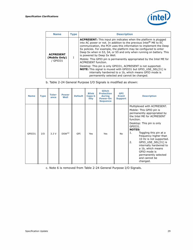
4. ACPRESENT/GPIO31 Definition
a. Table 2-8 Power Management Interface Signals is modified as shown:
Table 2-25 Desktop/Mobile Manageability Signals
Functionality Name Functionality Description Pin Name(s)1
SUSWARN# or SUSPWRDNACK (Mobile Only)
Used by Intel® ME as either SUSWARN# in Deep Sx state supported platforms or as SUSPWRDNACK in non Deep Sx state supported platforms.
SUSWARN# /SUSPWRDNACK#/
GPIO30
AC Present(Mobile Only)
Input signal from the Embedded Controller (EC) on Mobile systems to indicate AC power source or the system battery. Active High indicates AC power.
ACPRESENT / GPIO31
Temperature Alert
Used as an alert (active low) to indicate to the external controller (such as EC or SIO) that temperatures are out of range for the PCH or Graphics/Memory Controller or the processor core.
SATA5GP / GPIO49 / TEMP_ALERT#
Processor Missing(Desktop Only)
Used to indicate Processor Missing to the Intel Management Engine.
GPIO24 / PROC_MISSING
Table 2-26 Server Manageability Signals
Functionality Name Functionality Description MGPIO Name(s)1
SMBALERT# signal from PSU to PCH
Indicates the PSU may cause system shutdown due to a momentary loss of AC input voltage or an over temperature condition.
MGPIO2
Intel ME FW Recovery Mode
Strap Input to PCH to force Intel ME to stay in recovery boot loader.
MGPIO0, MGPIO1, MGPIO2, MGPIO3, MGPIO4, MGPIO5,
MGPIO6, MGPIO7, or MGPIO8
Table 2-27 Server MGPIO Signal to Pin Name Conversion Table
MGPIO Ballout Pin Name
MGPIO0 GPIO24/PROC_MISSING
MGPIO1 SUSWARN#/GPIO30
MGPIO2 GPIO31
MGPIO3 SLP_LAN#/GPIO29
MGPIO4 SML0ALERT#/GPIO60
MGPIO5 GPIO57
MGPIO6 GPIO27
MGPIO7 GPIO28
MGPIO8 SML1ALERT#/PCHHOT#/GPIO74
Specification Clarifications
Specification Update 29
b. Table 2-24 General Purpose I/O Signals is modified as shown:
c. Note 6 is removed from Table 2-24 General Purpose I/O Signals.
Name Type Description
ACPRESENT (Mobile Only)
/ GPIO31I
ACPRESENT: This input pin indicates when the platform is plugged into AC power or not. In addition to the previous Intel® ME to EC communication, the PCH uses this information to implement the Deep Sx policies. For example, the platform may be configured to enter Deep Sx when in S3, S4, or S5 and only when running on battery. This is powered by Deep Sx Well.Mobile: This GPIO pin is permanently appropriated by the Intel ME for ACPRESENT function.Desktop: This pin is only GPIO31, ACPRESENT is not supported.NOTE: This signal is muxed with GPIO31 but GPIO_USE_SEL[31] is
internally hardwired to a 1b, which means GPIO mode is permanently selected and cannot be changed.
Name Type Toler-ance
Power Well Default
Blink Capa-b
ility
Glitch Protection
during Power-On Sequence
GPI Event
SupportDescription
GPIO31 I/O 3.3 V DSW12 GPI Yes Yes No
Multiplexed with ACPRESENT.Mobile: This GPIO pin is permanently appropriated by the Intel ME for ACPRESENT function.Desktop: This pin is only GPIO31.NOTES:1. Toggling this pin at a
frequency higher than 10 Hz is not supported.
2. GPIO_USE_SEL[31] is internally hardwired to a 1b, which means GPIO mode is permanently selected and cannot be changed.

Specification Clarifications
30 Specification Update
5. SPI Overview
The Serial Peripheral Interface (SPI) subsection of section 1.2.1 Capability Overview is replaced as follows:
The PCH provides an SPI Interface and is required to be used on the platform in order to provide chipset configuration settings and Intel ME firmware. If integrated Gigabit Ethernet MAC/PHY is implemented on the platform, the interface is used for this device configuration settings. The interface may also be used as the interface for the BIOS flash device or alternatively a FWH on LPC may be used. The PCH supports up to two SPI flash devices using two chip select pins with speeds up to 50 MHz.
§ §

Documentation Changes
Specification Update 31
Documentation Changes
1. Integrated Digital Display Audio Revision ID Correction
The second paragraph of section 18.2.2 Integrated Digital Display Audio Device ID and Revision ID is changed to the following:
The integrated digital display codec Revision ID is 00h for all PCH steppings.
2. t200a Correction
In Table 8-38. Power Sequencing and Reset Signal Timings, t200a is changed from 1 ms to 1 us.
3. Function Level Reset Pending Status Register Correction
Section 10.1.3 FLRSTAT—Function Level Reset Pending Status Register is updated as shown:
4. Miscellaneous Documentation Correction
In section 22.1 Serial Peripheral Interface Memory Mapped Configuration Registers, the RCBA register cross reference is corrected to be Section 13.1.40 (the RCBA—Root Complex Base Address Register).
5. SPI Required Region Correction
The second paragraph of section 5.25.1.2.1 SPI Flash Regions is changed to the following:
Only three masters can access the four regions: Host processor running BIOS code, Integrated Gigabit Ethernet and Host processor running Gigabit Ethernet Software, and Intel Management Engine. The Flash Descriptor and Intel ME region are the only required regions. The Flash Descriptor has to be in Region 0 and Region 0 must be located in the first sector of Device 0 (offset 10).
Bit Description
31:24 Reserved
23FLR Pending Status for EHCI #1 (D29) — RO.0 = Function Level Reset is not pending.1 = Function Level Reset is pending.
22:16 Reserved
15FLR Pending Status for EHCI #2 (D26) — RO.0 = Function Level Reset is not pending.1 = Function Level Reset is pending.
14:0 Reserved

Documentation Changes
32 Specification Update
6. High Precision Event Timers Functional Description
a. The following replaces section 5.17:
5.17 High Precision Event Timers (HPET)
This function provides a set of timers that can be used by the operating system. The timers are defined such that the operating system may be able to assign specific timers to be used directly by specific applications. Each timer can be configured to cause a separate interrupt.
The PCH provides eight timers. The timers are implemented as a single counter, and each timer has its own comparator and value register. The counter increases monotonically. Each individual timer can generate an interrupt when the value in its value register matches the value in the main counter.
The registers associated with these timers are mapped to a memory space (much like the I/O APIC). However, it is not implemented as a standard PCI function. The BIOS reports to the operating system the location of the register space. The hardware can support an assignable decode space; however, the BIOS sets this space prior to handing it over to the operating system. It is not expected that the operating system will move the location of these timers once it is set by the BIOS.
5.17.1 Timer Accuracy1. The timers are accurate over any 1 ms period to within 0.05% of the time specified
in the timer resolution fields.2. Within any 100 microsecond period, the timer reports a time that is up to two ticks
too early or too late. Each tick is less than or equal to 100 ns, so this represents an error of less than 0.2%.
3. The timer is monotonic. It does not return the same value on two consecutive reads (unless the counter has rolled over and reached the same value).
The main counter is clocked by the 14.31818 MHz clock. The accuracy of the main counter is as accurate as the 14.31818 MHz clock.
5.17.2 Interrupt Mapping
The interrupts associated with the various timers have several interrupt mapping options. When reprogramming the HPET interrupt routing scheme (LEG_RT_CNF bit in the General Configuration Register), a spurious interrupt may occur. This is because the other source of the interrupt (8254 timer) may be asserted. Software should mask interrupts prior to clearing the LEG_RT_CNF bit.
Mapping Option #1 (Legacy Replacement Option)
In this case, the Legacy Replacement Rout bit (LEG_RT_CNF) is set. This forces the mapping found in Table 5-43.

Documentation Changes
Specification Update 33
NOTE: The Legacy Option does not preclude delivery of IRQ0/IRQ8 using processor message interrupts.
Mapping Option #2 (Standard Option)
In this case, the Legacy Replacement Rout bit (LEG_RT_CNF) is 0. Each timer has its own routing control. The interrupts can be routed to various interrupts in the 8259 or I/O APIC. A capabilities field indicates which interrupts are valid options for routing. If a timer is set for edge-triggered mode, the timers should not be shared with any PCI interrupts.
For the PCH, the only supported interrupt values are as follows:
Timer 0 and 1: IRQ20, 21, 22 & 23 (I/O APIC only).
Timer 2: IRQ11 (8259 or I/O APIC) and IRQ20, 21, 22 & 23 (I/O APIC only).
Timer 3: IRQ12 (8259 or I/O APIC) and IRQ 20, 21, 22 & 23 (I/O APIC only).
Interrupts from Timer 4, 5, 6, 7 can only be delivered using processor message interrupts.
Mapping Option #3 (Processor Message Option)
In this case, the interrupts are mapped directly to processor messages without going to the 8259 or I/O (x) APIC. To use this mode, the interrupt must be configured to edge-triggered mode. The Tn_PROCMSG_EN_CNF bit must be set to enable this mode.
When the interrupt is delivered to the processor, the message is delivered to the address indicated in the Tn_PROCMSG_INT_ADDR field. The data value for the write cycle is specified in the Tn_PROCMSG_INT_VAL field.
Notes:1. The processor message interrupt delivery option has HIGHER priority and is
mutually exclusive to the standard interrupt delivery option. Thus, if the Tn_PROCMSG_EN_CNF bit is set, the interrupts will be delivered directly to the processor rather than via the APIC or 8259.
2. The processor message interrupt delivery can be used even when the legacy mapping is used.
3. The IA-PC HPET Specification uses the term “FSB Interrupt” to describe these type of interrupts.
Table 5-43 Legacy Replacement Routing
Timer 8259 Mapping APIC Mapping Comment
0 IRQ0 IRQ2 In this case, the 8254 timer will not cause any interrupts
1 IRQ8 IRQ8 In this case, the RTC will not cause any interrupts.
2 & 3 Per IRQ Routing Field. Per IRQ Routing Field
4, 5, 6, 7 not available not available

Documentation Changes
34 Specification Update
5.17.3 Periodic vs. Non-Periodic Modes
Non-Periodic Mode
Timer 0 is configurable to 32 (default) or 64-bit mode, whereas Timers 1:7 only support 32-bit mode (See Section 21.1.5).
Warning: Software must be careful when programming the comparator registers. If the value written to the register is not sufficiently far in the future, then the counter may pass the value before it reaches the register and the interrupt will be missed. The BIOS should pass a data structure to the OS to indicate that the OS should not attempt to program the periodic timer to a rate faster than 5 microseconds.
All of the timers support non-periodic mode.
Refer to Section 2.3.9.2.1 of the IA-PC HPET Specification for more details of this mode.
Periodic Mode
Timer 0 is the only timer that supports periodic mode. Refer to Section 2.3.9.2.2 of the IA-PC HPET Specification for more details of this mode.
If the software resets the main counter, the value in the comparator’s value register needs to reset as well. This can be done by setting the TIMERn_VAL_SET_CNF bit. Again, to avoid race conditions, this should be done with the main counter halted. The following usage model is expected:1. Software clears the ENABLE_CNF bit to prevent any interrupts.2. Software Clears the main counter by writing a value of 00h to it.3. Software sets the TIMER0_VAL_SET_CNF bit.4. Software writes the new value in the TIMER0_COMPARATOR_VAL register.5. Software sets the ENABLE_CNF bit to enable interrupts.
The Timer 0 Comparator Value register cannot be programmed reliably by a single 64-bit write in a 32-bit environment except if only the periodic rate is being changed during run-time. If the actual Timer 0 Comparator Value needs to be re initialized, then the following software solution will always work regardless of the environment: 1. Set TIMER0_VAL_SET_CNF bit.2. Set the lower 32 bits of the Timer0 Comparator Value register.3. Set TIMER0_VAL_SET_CNF bit.4. Set the upper 32 bits of the Timer0 Comparator Value register.
5.17.4 Enabling the Timers
The BIOS or operating system PnP code should route the interrupts. This includes the Legacy Rout bit, Interrupt Rout bit (for each timer), and interrupt type (to select the edge or level type for each timer).
The Device Driver code should do the following for an available timer:1. Set the Overall Enable bit (Offset 10h, bit 0).2. Set the timer type field (selects one-shot or periodic).3. Set the interrupt enable.4. Set the comparator value.

Documentation Changes
Specification Update 35
5.17.5 Interrupt Levels
Interrupts directed to the internal 8259s are active high. See Section 5.9 for information regarding the polarity programming of the I/O APIC for detecting internal interrupts.
If the interrupts are mapped to the 8259 or I/O APIC and set for level-triggered mode, they can be shared with PCI interrupts.
If more than one timer is configured to share the same IRQ (using the TIMERn_INT_ROUT_CNF fields), then the software must configure the timers to level-triggered mode. Edge-triggered interrupts cannot be shared.
5.17.6 Handling Interrupts
Section 2.4.6 of the IA-PC HPET Specification describes Handling Interrupts.
5.17.7 Issues Related to 64-Bit Timers with 32-Bit Processors
Section 2.4.7 of the IA-PC HPET Specification describes Issues Related to 64-Bit Timers with 32-Bit Processors.
b. The following replaces section 5.29.5:
5.29.5 Virtualization Support for High Precision Event Timer (HPET)
The Intel VT-d architecture extension requires Interrupt Messages to go through the similar Address Remapping as any other memory requests. This is to allow domain isolation for interrupts such that a device assigned in one domain is not allowed to generate interrupts to another domain.
The Address Remapping for Intel VT-d is based on the Bus:Device:Function field associated with the requests. Hence, it is required for the HPET to initiate processor message interrupts using unique Bus:Device:Function.
The PCH supports BIOS programmable unique Bus:Device:Function for each of the HPET timers. The Bus:Device:Function field does not change the HPET functionality in anyway, nor promoting it as a stand-alone PCI device. The field is only used by the HPET timer in the following:
• As the Requestor ID when initiating processor message interrupts to the processor• As the Completer ID when responding to the reads targeting its Memory-Mapped
registers• The registers for the programmable Bus:Device:Function for HPET timer 7:0 reside
under the Device 31:Function 0 LPC Bridge’s configuration space.
7. Miscellaneous Documentation Corrections II
a. Remove “1.05 V Core Voltage” from Platform Controller Hub Features section.
b. The GPIO bullet in the Platform Controller Hub Features section is replaced with the following:
c. The first sentence of the seventh paragraph of section 1.1 About This Manual is changed to:
This manual assumes a working knowledge of the vocabulary and principles of interfaces and architectures such as PCI Express*, USB, AHCI, SATA, Intel® High Definition Audio (Intel® HD Audio), SMBus, PCI, ACPI and LPC.
GPIO—Inversion; Open-Drain (not available on all GPIOs)—GPIO lock down

Documentation Changes
36 Specification Update
d. Table 1-1 Industry Specifications is updated as follows:
1. The URL for IA-PC HPET (High Precision Event Timers) Specification, Revision 1.0a is changed to:
http://www.intel.com/content/www/us/en/software-developers/software-developers-hpet-spec-1-0a.html
2. The URL for SFF-8485 Specification for Serial GPIO (SGPIO) Bus, Revision 0.7 is changed to:
ftp://ftp.seagate.com/sff/SFF-8485.PDF
3. The URL for Advanced Host Controller Interface specification for Serial ATA, Revision 1.3 is changed to:
http://www.intel.com/content/www/us/en/io/serial-ata/serial-ata-ahci-spec-rev1_3.html
4. The URL for Intel® High Definition Audio Specification, Revision 1.0a is changed to:
http://www.intel.com/content/www/us/en/standards/standards-high-def-audio-specs-general-technology.html
e. The Function Disable bullet of the Manageability subsection of section 1.2.1 Capability Overview is replaced as follows:
Function Disable. The PCH provides the ability to disable most integrated functions, including integrated LAN, USB, LPC, Intel HD Audio, SATA, PCI Express, and SMBus. Once disabled, functions no longer decode I/O, memory, or PCI configuration space. Also, no interrupts or power management events are generated from the disabled functions.
f. Table 2-29 is updated to change “FVCEC0” to “FVEC0”. (See PCH Device and Revision Identification section in this document.)
g. The second paragraph of section 5.16.7 Intel® Rapid Storage Technology Configuration is replaced as follows:
By using the PCH’s built-in Intel Rapid Storage Technology, there is no loss of additional PCIe/system resources or add-in card slot/motherboard space footprint used compared to when a discrete RAID controller is implemented.
h. The fourth sentence of the first paragraph of section 5.19.1 [USB 2.0 RMH] Overview is replaces as follows:
The RMHs will appear to software like an external hub is connected to Port 0 of each EHCI controller.
i. Occurrences of ”DOCK_RST#” are changed to “HDA_DOCK_RST#”.
j. Figure 8-1 G3 w/RTC Loss to S4/S5 (With Deep Sx Support) Timing Diagram and figure 8-2 G3 w/RTC Loss to S4/S5 (Without Deep Sx Support) Timing Diagram are updated to remove t226.
k. Default value for USBOCM1 in table 10-1 Chipset Configuration Register Memory Map is changed from 0300C03h to C0300C03h.
l. The default value for section 10.1.41 D22IP—Device 22 Interrupt Pin Register is changed from 00000001h to 00004321h.
m. R/W/V attribute is changed to R/W.

Documentation Changes
Specification Update 37
n. R/W/C attribute is changed to R/WC.
o. Section 24.1.1.12 INTR—Interrupt Information Register (Intel® MEI 1—D22:F0) is updated as shown:Default Value: 0100h Size: 16 bits
p. Section 24.1.1.25 HIDM—MEI Interrupt Delivery Mode Register (Intel® MEI 1—D22:F0)
q. Section 24.2.1.12 INTR—Interrupt Information Register (Intel® MEI 2—D22:F1)
r. Section 24.2.1.24 HIDM—Intel® MEI Interrupt Delivery Mode Register (Intel® MEI 2—D22:F1)
Bit Description
15:8
Interrupt Pin (IPIN) — RO. This indicates the interrupt pin the Intel MEI host controller uses. A value of 1h/2h/3h/4h indicates that this function implements legacy interrupt on INTA/INTB/INTC/INTD, respectively. The upper 4 bits are hardwired to 0 and the lower 4 bits are programmed by the MEI1IP bits (RCBA+3124:bits 3:0).
7:0 Interrupt Line (ILINE) — R/W. Software written value to indicate which interrupt line (vector) the interrupt is connected to. No hardware action is taken on this register.
Bit Description
7:2 Reserved
1:0
Intel MEI Interrupt Delivery Mode (HIDM) — R/W. These bits control what type of interrupt the Intel MEI will send the host. They are interpreted as follows:00 = Generate Legacy or MSI interrupt01 = Generate SCI10 = Generate SMI
Bit Description
15:8
Interrupt Pin (IPIN) — RO. This indicates the interrupt pin the Intel MEI host controller uses. A value of 1h/2h/3h/4h indicates that this function implements legacy interrupt on INTA/INTB/INTC/INTD, respectively. The upper 4 bits are hardwired to 0 and the lower 4 bits are programmed by the MEI2IP bits (RCBA+3124:bits 7:4).
7:0 Interrupt Line (ILINE) — R/W. Software written value to indicate which interrupt line (vector) the interrupt is connected to. No hardware action is taken on this register.
Bit Description
7:2 Reserved
1:0
Intel MEI Interrupt Delivery Mode (HIDM) — R/W. These bits control what type of interrupt the Intel MEI will send the host. They are interpreted as follows:00 = Generate Legacy or MSI interrupt01 = Generate SCI10 = Generate SMI
Documentation Changes
38 Specification Update
s. Section 24.3.1.16 INTR—Interrupt Information Register (IDER—D22:F2)
t. Section 24.4.1.13 INTR—Interrupt Information Register (KT—D22:F3)Default Value: 0400h Size: 16 bits
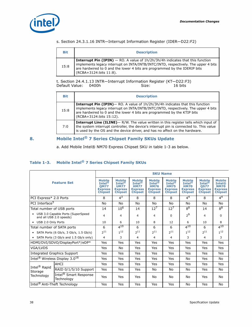
8. Mobile Intel® 7 Series Chipset Family SKUs Update
a. Add Mobile Intel® NM70 Express Chipset SKU in table 1-3 as below.
Table 1-3. Mobile Intel® 7 Series Chipset Family SKUs
Bit Description
15:8
Interrupt Pin (IPIN) — RO. A value of 1h/2h/3h/4h indicates that this function implements legacy interrupt on INTA/INTB/INTC/INTD, respectively. The upper 4 bits are hardwired to 0 and the lower 4 bits are programmed by the IDERIP bits (RCBA+3124:bits 11:8).
Bit Description
15:8
Interrupt Pin (IPIN)— RO. A value of 1h/2h/3h/4h indicates that this function implements legacy interrupt on INTA/INTB/INTC/INTD, respectively. The upper 4 bits are hardwired to 0 and the lower 4 bits are programmed by the KTIP bits (RCBA+3124:bits 15:12).
7:0Interrupt Line (ILINE)— R/W. The value written in this register tells which input of the system interrupt controller, the device's interrupt pin is connected to. This value is used by the OS and the device driver, and has no affect on the hardware.
Feature Set
SKU Name
Mobile Intel® QM77
Express Chipset
Mobile Intel® UM77
Express Chipset
Mobile Intel® HM77
Express Chipset
Mobile Intel® HM76
Express Chipset
Mobile Intel® HM75
Express Chipset
Mobile Intel® HM70
Express Chipset
Mobile Intel® QS77
Express Chipset
Mobile Intel® NM70
Express Chipset
PCI Express* 2.0 Ports 8 43 8 8 8 44 8 44
PCI Interface5 No No No No No No No NoTotal number of USB ports 14 106 14 127 127 88 14 88
• USB 3.0 Capable Ports (SuperSpeed and all USB 2.0 speeds) 4 4 4 4 0 29 4 0
• USB 2.0 Only Ports 10 6 10 8 12 6 10 8
Total number of SATA ports 6 410 6 6 6 410 6 410
• SATA Ports (6 Gb/s, 3 Gb/s, 1.5 Gb/s) 211 112 211 211 211 112 211 112
• SATA Ports (3 Gb/s and 1.5 Gb/s only) 4 3 4 4 4 3 4 3
HDMI/DVI/SDVO/DisplayPort*/eDP* Yes Yes Yes Yes Yes Yes Yes YesVGA/LVDS Yes No Yes Yes Yes Yes Yes YesIntegrated Graphics Support Yes Yes Yes Yes Yes Yes Yes YesIntel® Wireless Display 3.016 Yes Yes Yes Yes Yes No Yes No
Intel® Rapid Storage Technology
AHCI Yes Yes Yes Yes Yes Yes Yes YesRAID 0/1/5/10 Support Yes Yes Yes No No No Yes NoIntel® Smart Response Technology Yes Yes Yes No No No Yes No
Intel® Anti-Theft Technology Yes Yes Yes Yes Yes No Yes No

Documentation Changes
Specification Update 39
§ §
Intel® Active Management Technology 8.0 Yes No No No No No Yes13 No
Intel® Small Business Advantage Yes Yes13 Yes13 No No No Yes13, 14 NoIntel® Rapid Start Technology15 Yes Yes Yes Yes Yes Yes Yes NoACPI S1 State Support Yes Yes Yes Yes Yes Yes Yes Yes
Feature Set
SKU Name
Mobile Intel® QM77
Express Chipset
Mobile Intel® UM77
Express Chipset
Mobile Intel® HM77
Express Chipset
Mobile Intel® HM76
Express Chipset
Mobile Intel® HM75
Express Chipset
Mobile Intel® HM70
Express Chipset
Mobile Intel® QS77
Express Chipset
Mobile Intel® NM70
Express Chipset

Documentation Changes
40 Specification Update