Embed Size (px)
Citation preview

Intel® E7500 ChipsetDatasheet
Intel® E7500 Memory Controller Hub (MCH)
February 2002
Document Number: 290730-001

2 Datasheet
Information in this document is provided in connection with Intel® products. No license, express or implied, by estoppel or otherwise, to any intellectual property rights is granted by this document. Except as provided in Intel's Terms and Conditions of Sale for such products, Intel assumes no liability whatsoever, and Intel disclaims any express or implied warranty, relating to sale and/or use of Intel products including liability or warranties relating to fitness for a particular purpose, merchantability, or infringement of any patent, copyright or other intellectual property right. Intel products are not intended for use in medical, life saving, or life sustaining applications.
Intel may make changes to specifications and product descriptions at any time, without notice.
Designers must not rely on the absence or characteristics of any features or instructions marked "reserved" or "undefined." Intel reserves these for future definition and shall have no responsibility whatsoever for conflicts or incompatibilities arising from future changes to them.
The Intel® E7500 chipset MCH component may contain design defects or errors known as errata which may cause the product to deviate from published specifications. Current characterized errata are available on request.
Contact your local Intel sales office or your distributor to obtain the latest specifications and before placing your product order.
Copies of documents which have an ordering number and are referenced in this document, or other Intel literature, may be obtained by calling 1-800-548-4725 or by visiting Intel's website at http://www.intel.com.
IIntel, Intel NetBurst and the Intel logo are trademarks or registered trademarks of Intel corporation or its subsidiaries in the United States and other countries.
*Other names and brands may be claimed as the property of others.
Copyright© 2002, Intel Corporation

Contents1 Introduction ................................................................................................................11
1.1 Glossary of Terms ...............................................................................................111.2 Reference Documents.........................................................................................121.3 Intel® E7500 Chipset System Architecture..........................................................12
1.3.1 Intel® 82801CA I/O Controller Hub 3-S (ICH3-S)...................................131.3.2 Intel® 82870P2 PCI/PCI-X 64-bit Hub 2 (P64H2)...................................14
1.4 Intel® E7500 MCH Overview...............................................................................141.4.1 Processor System Interface ...................................................................151.4.2 Main Memory Interface...........................................................................151.4.3 Hub Interface_A (HI_A) ..........................................................................151.4.4 Hub Interface_B–D (HI_B–D).................................................................161.4.5 MCH Clocking ........................................................................................161.4.6 SMBus Interface.....................................................................................16
2 Signal Description ...................................................................................................172.1 System Bus Interface Signals .............................................................................192.2 DDR Channel A Signals ......................................................................................222.3 DDR Channel B Signals ......................................................................................232.4 Hub Interface_A Signals......................................................................................242.5 Hub Interface_B Signals......................................................................................252.6 Hub Interface_C Signals .....................................................................................262.7 Hub Interface_D Signals .....................................................................................272.8 Clocks, Reset, Power, and Miscellaneous Signals .............................................282.9 Pin States During and After Reset ......................................................................28
3 Register Description ...............................................................................................313.1 Register Terminology ..........................................................................................313.2 Platform Configuration.........................................................................................323.3 General Routing Configuration Accesses ...........................................................33
3.3.1 Standard PCI Configuration Mechanism ................................................333.3.2 Logical PCI Bus 0 Configuration Mechanism .........................................343.3.3 Primary PCI Downstream Configuration Mechanism .............................343.3.4 HI_B, HI_C, HI_D Bus Configuration Mechanism ..................................34
3.4 Sticky Registers...................................................................................................353.5 I/O Mapped Registers .........................................................................................35
3.5.1 CONF_ADDR—Configuration Address Register ...................................353.5.2 CONF_DATA—Configuration Data Register..........................................36
3.6 DRAM Controller Registers (Device 0, Function 0).............................................373.6.1 VID—Vendor Identification Register (D0:F0) .........................................383.6.2 DID—Device Identification Register (D0:F0)..........................................383.6.3 PCICMD—PCI Command Register (D0:F0) ..........................................393.6.4 PCISTS—PCI Status Register (D0:F0) ..................................................403.6.5 RID—Revision Identification Register (D0:F0) .......................................413.6.6 SUBC—Sub-Class Code Register (D0:F0) ............................................413.6.7 BCC—Base Class Code Register (D0:F0).............................................413.6.8 MLT—Master Latency Timer Register (D0:F0) ......................................42
Datasheet 3

3.6.9 HDR—Header Type Register (D0:F0).................................................... 423.6.10 SVID—Subsystem Vendor Identification Register (D0:F0) .................... 423.6.11 SID—Subsystem Identification Register (D0:F0) ................................... 433.6.12 MCHCFG—MCH Configuration Register (D0:F0)..................................433.6.13 MCHCFGNS—MCH Memory Scrub and Initialization Configuration
Register (D0:F0)..................................................................................... 453.6.14 FDHC—Fixed DRAM Hole Control Register (D0:F0)............................. 463.6.15 PAM[0:6]—Programmable Attribute Map Registers (D0:F0).................. 473.6.16 DRB—DRAM Row Boundary Register (D0:F0) ..................................... 493.6.17 DRA—DRAM Row Attribute Register (D0:F0) ....................................... 503.6.18 DRT—DRAM Timing Register (D0:F0) .................................................. 513.6.19 DRC—DRAM Controller Mode Register (D0:F0) ................................... 523.6.20 CLOCK_DIS—CK/CK# Disable Register (D0:F0)..................................533.6.21 SMRAM—System Management RAM Control Register (D0:F0) ........... 543.6.22 ESMRAMC—Extended System Management RAM Control Register
(D0:F0) ...................................................................................................553.6.23 TOLM—Top of Low Memory Register (D0:F0) ...................................... 563.6.24 REMAPBASE—Remap Base Address Register (D0:F0)....................... 563.6.25 REMAPLIMIT—Remap Limit Address Register (D0:F0)........................ 573.6.26 SKPD—Scratchpad Data Register (D0:F0)............................................ 573.6.27 DVNP—Device Not Present Register (D0:F0) ....................................... 58
3.7 DRAM Controller Error Reporting Registers (Device 0, Function 1) ................... 593.7.1 VID—Vendor Identification Register (D0:F1) .........................................603.7.2 DID—Device Identification Register (D0:F1).......................................... 603.7.3 PCICMD—PCI Command Register (D0:F1) .......................................... 613.7.4 PCISTS—PCI Status Register (D0:F1).................................................. 613.7.5 RID—Revision Identification Register (D0:F1) ....................................... 623.7.6 SUBC—Sub-Class Code Register (D0:F1) ............................................ 623.7.7 BCC—Base Class Code Register (D0:F1)............................................. 633.7.8 MLT—Master Latency Timer Register (D0:F1) ...................................... 633.7.9 HDR—Header Type (D0:F1) ..................................................................643.7.10 SVID—Subsystem Vendor Identification Register (D0:F1) .................... 653.7.11 SID—Subsystem Identification Register (D0:F1) ................................... 653.7.12 FERR_GLOBAL—Global Error Register (D0:F1)................................... 663.7.13 NERR_GLOBAL—Global Error Register (D0:F1) ..................................673.7.14 HIA_FERR—Hub Interface_A First Error Register (D0:F1) ................... 683.7.15 HIA_NERR—Hub Interface_A Next Error Register (D0:F1)................... 693.7.16 SCICMD_HIA—SCI Command Register (D0:F1) ..................................703.7.17 SMICMD_HIA—SMI Command Register (D0:F1)..................................713.7.18 SERRCMD_HIA—SERR Command Register (D0:F1) .......................... 723.7.19 SYSBUS_FERR—System Bus First Error Register (D0:F1).................. 733.7.20 SYSBUS_NERR—System Bus Next Error Register (D0:F1)................. 743.7.21 SCICMD_SYSBUS—SCI Command Register (D0:F1).......................... 753.7.22 SMICMD_SYSBUS—SMI Command Register (D0:F1) ......................... 763.7.23 SERRCMD_SYSBUS—SERR Command Register (D0:F1).................. 773.7.24 DRAM_FERR—DRAM First Error Register (D0:F1) .............................. 783.7.25 DRAM_NERR—DRAM Next Error Register (D0:F1) ............................. 783.7.26 SCICMD_DRAM—SCI Command Register (D0:F1).............................. 793.7.27 SMICMD_DRAM—SMI Command Register (D0:F1) ............................. 793.7.28 SERRCMD_DRAM—SERR Command Register (D0:F1)...................... 80
4 Datasheet

3.7.29 DRAM_CELOG_ADD—DRAM First Correctable Memory Error Address Register (D0:F1).......................................................................80
3.7.30 DRAM_UELOG_ADD—DRAM First Uncorrectable Memory Error Address Register (D0:F1).......................................................................81
3.7.31 DRAM_CELOG_SYNDROME—DRAM First Correctable Memory Error Register (D0:F1)............................................................................81
3.8 HI_B Virtual PCI-to-PCI Bridge Registers (Device 2, Function 0) .......................823.8.1 VID2—Vendor Identification Register (D2:F0) .......................................833.8.2 DID2—Device Identification Register (D2:F0)........................................833.8.3 PCICMD2—PCI Command Register (D2:F0) ........................................843.8.4 PCISTS2—PCI Status Register (D2:F0) ................................................853.8.5 RID2—Revision Identification Register (D2:F0) .....................................863.8.6 SUBC2—Sub-Class Code Register (D2:F0) ..........................................863.8.7 BCC2—Base Class Code Register (D2:F0)...........................................873.8.8 MLT2—Master Latency Timer Register (D2:F0) ....................................873.8.9 HDR2—Header Type Register (D2:F0)..................................................883.8.10 PBUSN2—Primary Bus Number Register (D2:F0) ................................883.8.11 BUSN2—Secondary Bus Number Register (D2:F0) ..............................893.8.12 SUBUSN2—Subordinate Bus Number Register (D2:F0).......................893.8.13 SMLT2—Secondary Bus Master Latency Timer Register (D2:F0) ........903.8.14 IOBASE2—I/O Base Address Register (D2:F0).....................................913.8.15 IOLIMIT2—I/O Limit Address Register (D2:F0)......................................913.8.16 SEC_STS2—Secondary Status Register (D2:F0) .................................923.8.17 MBASE2—Memory Base Address Register (D2:F0) .............................933.8.18 MLIMIT2—Memory Limit Address Register (D2:F0) ..............................943.8.19 PMBASE2—Prefetchable Memory Base Address Register (D2:F0)......953.8.20 PMLIMIT2—Prefetchable Memory Limit Address Register (D2:F0).......953.8.21 BCTRL2—Bridge Control Register (D2:F0) ...........................................96
3.9 HI_B Virtual PCI-to-PCI Bridge Registers (Device 2, Function 1) .......................973.9.1 VID—Vendor Identification Register (D2:F1) .........................................983.9.2 DID—Device Identification Register (D2:F1)..........................................983.9.3 PCICMD—PCI Command Register (D2:F1) ..........................................993.9.4 PCISTS—PCI Status Register (D2:F1) ..................................................993.9.5 RID—Revision Identification Register (D2:F1) .....................................1003.9.6 SUBC—Sub-Class Code Register (D2:F1) ..........................................1003.9.7 BCC—Base Class Code Register (D2:F1)...........................................1013.9.8 HDR—Header Type Register (D2:F1)..................................................1013.9.9 SVID—Subsystem Vendor Identification Register (D2:F1) ..................1023.9.10 SID—Subsystem Identification Register (D2:F1) .................................1023.9.11 HIB_FERR—Hub Interface_B First Error Register (D2:F1) .................1033.9.12 HIB_NERR—Hub Interface_B Next Error Register (D2:F1).................1043.9.13 SERRCMD2—SERR Command Register (D2:F1) ..............................1053.9.14 SMICMD2—SMI Command Register (D2:F1)......................................1063.9.15 SCICMD2—SCI Command Register (D2:F1) ......................................107
3.10 HI_C Virtual PCI-to-PCI Bridge Registers (Device 3, Function 0,1)..................1083.10.1 DID—Device Identification Register (D3:F0)........................................1083.10.2 DID—Device Identification Register (D3:F1)........................................108
3.11 HI_D Virtual PCI-to-PCI Bridge Registers (Device 4, Function 0,1)..................1093.11.1 DID—Device Identification Register (D4:F0)........................................1093.11.2 DID—Device Identification Register (D4:F1)........................................109
Datasheet 5

4 System Address Map............................................................................................ 1114.1 System Memory Spaces ................................................................................... 111
4.1.1 VGA and MDA Memory Spaces........................................................... 1134.1.2 PAM Memory Spaces .......................................................................... 1144.1.3 ISA Hole Memory Space...................................................................... 1154.1.4 I/O APIC Memory Space...................................................................... 1154.1.5 System Bus Interrupt Memory Space................................................... 1154.1.6 Device 2 Memory and Prefetchable Memory .......................................1154.1.7 Device 3 Memory and Prefetchable Memory .......................................1164.1.8 Device 4 Memory and Prefetchable Memory .......................................1164.1.9 HI_A Subtractive Decode..................................................................... 1164.1.10 Main Memory Addresses...................................................................... 116
4.2 I/O Address Space ............................................................................................ 1174.3 SMM Space.......................................................................................................117
4.3.1 System Management Mode (SMM) Memory Range............................ 1174.3.2 TSEG SMM Memory Space................................................................. 1184.3.3 High SMM Memory Space ................................................................... 1184.3.4 SMM Space Restrictions...................................................................... 1184.3.5 SMM Space Definition.......................................................................... 119
4.4 Memory Reclaim Background ........................................................................... 1204.4.1 Memory Re-Mapping............................................................................ 120
5 Reliability, Availability, Serviceability, Usability, and Manageability (RASUM)....................................................................................... 1215.1 DRAM ECC .......................................................................................................1215.2 DRAM Scrubbing .............................................................................................. 1215.3 DRAM Auto-Initialization ................................................................................... 1215.4 SMBus Access .................................................................................................. 121
6 Electrical Characteristics....................................................................................1236.1 Absolute Maximum Ratings .............................................................................. 1236.2 Thermal Characteristics ....................................................................................1236.3 Power Characteristics ....................................................................................... 1246.4 I/O Interface Signal Groupings.......................................................................... 1256.5 DC Characteristics ............................................................................................ 127
7 Ballout and Package Specifications............................................................... 1317.1 Ballout ............................................................................................................... 1317.2 Package Specifications ..................................................................................... 1417.3 Chipset Interface Trace Length Compensation................................................. 143
7.3.1 MCH System Bus Signal Package Trace Length Data ........................ 1447.3.1.1 MCH DDR Channel A Signal Package Trace Length Data..... 1457.3.1.2 MCH DDR Channel B Signal Package Trace Length Data..... 1487.3.1.3 MCH Hub Interface_A Signal Package Trace Length
Data......................................................................................... 1517.3.1.4 MCH Hub Interface_B Signal Package Trace Length
Data......................................................................................... 1517.3.1.5 MCH Hub Interface_C Signal Package Trace Length
Data......................................................................................... 1527.3.1.6 MCH Hub Interface_D Signal Package Trace Length
Data......................................................................................... 152
6 Datasheet

8 Testability ..................................................................................................................1538.1 XOR Chains ......................................................................................................154
Figures1-1 Intel® E7500 Chipset Platform Block Diagram ....................................................132-1 MCH Interface Signals ........................................................................................183-1 PAM Registers ....................................................................................................484-1 System Address Map ........................................................................................1114-2 Detailed Extended Memory Range Address Map .............................................1127-1 Intel® E7500 MCH Ballout (Top View) ..............................................................1317-2 Intel® E7500 MCH Ballout (Left Half of Top View) ............................................1327-3 Intel® E7500 MCH Ballout (Right Half of Top View)..........................................1337-4 MCH Package Dimensions (Top View) .............................................................1417-5 MCH Package Dimensions (Side View) ............................................................142
Tables1-1 Supported DIMM Configuration...........................................................................152-1 System Bus Interface Signals .............................................................................192-2 DDR Channel_A Interface Signals ......................................................................222-3 DDR Channel_B Interface Signals ......................................................................232-4 HI _A Signals.......................................................................................................242-5 HI_B Signals........................................................................................................252-6 HI_C Signals .......................................................................................................262-7 HI_D Signals .......................................................................................................272-8 Clocks, Reset, Power, and Miscellaneous Signals .............................................283-1 Intel® E7500 MCH Logical Configuration Resources..........................................333-2 DRAM Controller Register Map (HI_A—D0:F0) ..................................................373-3 PAM Associated Attribute Bits.............................................................................483-4 DRAM Controller Register Map (HI_A—D0:F1) ..................................................593-5 HI_B Virtual PCI-to-PCI Bridge Register Map (HI_A—D2:F0) ............................823-6 HI_B Virtual PCI-to-PCI Bridge Register Map (HI_A—D2:F1) ............................974-1 SMM Address Range ........................................................................................1196-1 Absolute Maximum Ratings...............................................................................1236-2 MCH Package Thermal Resistance ..................................................................1236-3 Thermal Power Dissipation (VCC1_2 = 1.2 V ±5%)..........................................1246-4 DC Characteristics Functional Operating Range (VCC1_2 = 1.2 V ±5%).........1246-5 Signal Groups System Bus Interface ................................................................1256-6 Signal Groups DDR Interface............................................................................1256-7 Signal Groups Hub Interface 2.0 (HI_B–D) .......................................................1266-8 Signal Groups Hub Interface 1.5 (HI_A)............................................................1266-9 Signal Groups SMBus .......................................................................................1266-10 Signal Groups Reset and Miscellaneous ..........................................................1266-11 Operating Condition Supply Voltage (VCC1_2 = 1.2 V ±5%)............................1276-12 System Bus Interface (VCC1_2 = 1.2 V ±5%)...................................................1276-13 DDR Interface (VCC1_2 = 1.2 V ±5%)..............................................................1286-14 Hub Interface 2.0 Configured for 50 Ω (VCC1_2 = 1.2 V ±5%).........................1296-15 Hub Interface 1.5 with Parallel Buffer Mode Configured for 50 Ω
(VCC1_2 = 1.2 V ±5%)......................................................................................130
Datasheet 7
7-1 MCH Signal List ................................................................................................ 1347-2 Example Normalization Table ........................................................................... 1437-3 MCH LPKG Data for the System Bus ................................................................. 1447-4 MCH LPKG Data for DDR Channel A................................................................. 1457-5 MCH LPKG Data for DDR Channel B................................................................. 1487-6 MCH LPKG Data for Hub Interface_A ................................................................1517-7 MCH LPKG Data for Hub Interface_B ................................................................1517-8 MCH LPKG Data for Hub Interface_C ................................................................1527-9 MCH LPKG Data for Hub Interface_D ................................................................1528-1 XOR Chains ...................................................................................................... 154
8 Datasheet

Revision HistoryRev. Description Date
-001 Initial Release February 2002
Datasheet 9

Intel® E7500 MCH Features Processor/Host Bus Support
—Intel® Xeon™ processor with 512-KB L2 cache
—400 MHz system bus (2x address, 4x data)
—Symmetric Multiprocessing Protocol (SMP) for up to two processors at 400 MT/s
—System bus Dynamic Bus Inversion (DBI)
—36-bit system bus addressing—12-deep in-order queue—AGTL+ bus driver technology with
on-die termination resistors—Parity protection on system bus data,
address/request, and response signals Memory System
—One 144-bit wide DDR memory port (with Chipkill* technology ECC)
—Peak memory bandwidth of 3.2 GB/s—Supports 64 Mb, 128 Mb, 256 Mb,
512 Mb DRAM densities—Supports a maximum of 16 GB of
memory using (x4) double-sided DIMM—Supports x72, Registered, ECC DDR
DIMMs (in pairs) Hub Interface_A to Intel® ICH3-S
—Supports connection to ICH3-S via hub interface 1.5
—266 MB/s point-to-point hub interface 1.5 interface to ICH3-S
—Parity protected—66 MHz base clock running 4x
(533 MB/s) data transfer—Isochronous support—Parallel termination mode only—64-bit addressing on inbound
transactions (maximum 16 GB memory decode space)
Hub Interface_B, Hub Interface_C, and Hub Interface_D—Supports connection to Intel® P64H2 via
HI 2.0—Each hub interface is an independent
1 GB/s point-to-point 16-bit connection—ECC protected—66 MHz base clock running 8x (1 GB/s)
data transfers—Supports snooped and non-snooped
inbound accesses—Parallel termination mode—64-bit inbound addressing—32-bit outbound addressing supported
for PCI-X PCI / PCI-X
—Supports 33 MHz PCI on ICH3-S—Supports 33 MHz and 66 MHz PCI on
P64H2—Supports 66 MHz, 100 MHz or
133 MHz PCI-X on P64H2 RASUM
—Supports S4EC/D4ED ECC—Provides x4 Chipkill technology ECC
support—Correct any number of errors contained
in a 4-bit nibble —Detect all errors contained entirely
within two 4-bit nibbles—Hub Interface_A protected by parity—Hub Interface_B–D protected by ECC—Memory auto-initialization by hardware
implemented to allow main memory to be initialized with valid ECC
—Memory scrubbing supported—SMBus target interface access to MCH
error registers —P64H2 and ICH3-S have SMBus target
interface for access to registers—ICH3-S master SMBus interface reads
serial presence detect (SPD) on DIMMs Package
—1005-ball, 42.5 mm FC-BGA package
10 Datasheet

Introduction
Introduction 1
The Intel® E7500 chipset is targeted for the server market, both front-end and general purpose low- to mid-range. It is intended to be used with the Intel® Xeon™ processor with 512-KB L2 cache. The E7500 chipset consists of three major components: the Intel® E7500 Memory Controller Hub (MCH), the Intel® I/O Controller Hub 3 (ICH3-S), and the PCI/PCI-X 64-bit Hub 2.0 (P64H2). The MCH provides the system bus interface, memory controller, hub interface for legacy I/O, and three high-performance hub interfaces for PCI/PCI-X bus expansion.
This document describes the E7500 Memory Controller Hub (MCH). Section 1.3, “Intel® E7500 Chipset System Architecture” on page 1-12 provides an overview of each of the components of the E7500 chipset. For details on other components of the chipset, refer to that component’s datasheet.
1.1 Glossary of Terms
Term Description
DBI Dynamic Bus Inversion.
DDR Double Data Rate memory technology.
DP Dual Processor.
Full Reset The term “a full MCH reset” is used in this document when RSTIN# is asserted.
HI
Hub Interface. The proprietary hub interconnect that ties the MCH to the ICH3-S and P64H2. In this document HI cycles originating from or destined for the primary PCI interface on the ICH3-S are generally referred to as HI/PCI_A or simply HI_A cycles. Cycles originating from or destined for any target on the second, third or fourth HI interfaces are described as HI_B, HI_C, and HI_D cycles respectively. Note that there are two versions of HI used on the Intel® E7500 MCH: an 8-bit HI 1.5 protocol is implemented on HI_A and a 16-bit HI 2.0 protocol is used for the HI_B, HI_C and HI_D.
Host This term is used synonymously with processor.
IB Inbound, refers to traffic moving from PCI or other I/O toward DRAM or the system bus.
ICH3-SThe I/O Controller Hub 3-S component that contains the primary PCI interface, LPC interface, USB, ATA-100, and other legacy functions. It communicates with the MCH over a proprietary interconnect called the hub interface.
Intel® Xeon™ processor with 512-KB L2 cache
The processor supported by the Intel® E7500 chipset. This processor is the second generation of processors based on the Intel® NetBurst™ microarchitecture. This processor delivers performance levels that are significantly higher than previous generations of IA-32 processors. This processor supports 1-2 processors on a single system bus and has a 512 KB integrated L2 cache.
MCHThe Memory Controller Hub component that contains the processor interface and DRAM interface. It communicates with the I/O Controller Hub 3-S (ICH3-S) and P64H2 over a proprietary interconnect called the Hub Interface (HI).
OB Outbound, refers to traffic moving from the system bus to PCI or other I/O.
Intel® P64H2PCI/PCI-X 64-bit Hub 2.0 component. The Bus Controller Hub component has a 16-bit hub interconnect 2.0 on its primary side and two, 64-bit PCI-X bus segments on the secondary side.
Datasheet 11

Introduction
1.2 Reference Documents
NOTE: Refer to the Intel® Xeon™ Processor with 512-KB L2 Cache and Intel® E7500 Chipset Platform Design Guide for an expanded set of reference documents.
1.3 Intel® E7500 Chipset System ArchitectureThe E7500 chipset is optimized for the Intel Xeon processor with 512-KB L2 cache. The architecture of the chipset provides the performance and feature-set required for dual-processor based severs in the entry-level and mid-range, front-end and general-purpose server market segments. A new chipset component interconnect, the hub interface 2.0 (HI2.0), is designed into the E7500 chipset to provide more efficient communication between chipset components for high-speed I/O. Each HI2.0 provides 1.066 GB/s I/O bandwidth. The E7500 chipset has three HI2.0 connections, delivering 3.2 GB/s bandwidth for high-speed I/O, which can be used for PCI-X. The system bus, used to connect the processor with the E7500 chipset, utilizes a 400 MT/s transfer rate for data transfers, delivering a bandwidth of 3.2 GB/s. The E7500 chipset architecture supports a 144-bit wide, 200 MHz Double Data Rate (DDR) memory interface also capable of transferring data at 3.2 GB/s.
In addition to these performance features, E7500 chipset-based platforms also provide the RASUM (Reliability, Availability, Serviceability, Usability, and Manageability) features required for entry-level and mid-range servers. These features include: Chipkill* technology ECC for memory, ECC for all high-performance I/O, out-of-bound manageability through SMBus target interfaces on all major components, memory scrubbing and auto-initialization, processor thermal monitoring, and hot-plug PCI/PCI-X.
Primary PCI or PCI_A
The physical PCI bus that is driven directly by the ICH3-S component. It supports 5 V, 32-bit, 33 MHz PCI 2.2 compliant components. Communication between PCI_A and the MCH occurs over HI_A. Note that even though the Primary PCI bus is referred to as PCI_A it is not PCI Bus #0 from a configuration standpoint.
RASUM Reliability, Availability, Serviceability, Usability and Manageability.
Document Document Number
Intel® Xeon™ Processor with 512 KB L2 Cache and Intel® E7500 Chipset Platform Design Guide 298649
Intel® 82801CA I/O Controller Hub 3-S (ICH3-S) Datasheet 290733
Intel® 82870P2 PCI/PCI-X 64-bit Hub 2 (P64H2) Datasheet 290732
Intel® E7500 Chipset: E7500 Memory Controller Hub (MCH) Thermal and Mechanical Design Guidelines 298647
Intel® PCI/PCI-X 64-bit Hub 2 (P64H2) Thermal and Mechanical Design Guidelines 298648
Intel® 82802B/AC Firmware Hub (FWH) Datasheet 290658
Intel® Xeon™ Processor with 512-KB L2 Cache Datasheet
Term Description
12 Datasheet

Introduction
The E7500 chipset consists of three major components: the Memory Controller Hub (MCH), the I/O Controller Hub 3-S (ICH3-S), and the PCI/PCI-X 64-bit Hub 2.0 (P64H2). The chipset components communicate via hub interfaces (HIs). The MCH provides four hub interface connections: one for the ICH3-S and three for high-speed I/O using P64H2 bridges. The hub interfaces are point-to-point and therefore only support two agents (the MCH plus one I/O device), providing connections for up to 3 P64H2 bridges. The P64H2 provides bridging functions between hub interface_B–D and the PCI/PCI-X bus. Up to six PCI-X busses are supported. Each PCI-X bus is 66 MHz, 100 MHz, and 133 MHz PCI-X capable.
Additional platform features supported by the E7500 chipset include four ATA/100 IDE drives, Low Pin Count interface (LPC), integrated LAN Controller, Audio Codec, and Universal Serial Bus (USB).
The E7500 chipset is also ACPI compliant and supports Full-on, Stop Grant, Suspend to Disk, and Soft-off power management states. Through the use of an appropriate LAN device, the E7500 chipset also supports wake-on-LAN* for remote administration and troubleshooting.
1.3.1 Intel® 82801CA I/O Controller Hub 3-S (ICH3-S)The ICH3-S is a highly-integrated, multi-functional I/O Controller Hub that provides the interface to the PCI bus and integrates many of the functions needed in today’s PC platforms. The MCH and ICH3-S communicate over a dedicated hub interface. Intel 82801CA ICH3-S functions and capabilities include:
• PCI Local Bus Specification, Revision 2.2-compliant with support for 33 MHz PCI operations.
• PCI slots (supports up to 6 Req/Gnt pairs)
• ACPI Power Management Logic Support
• Enhanced DMA Controller, Interrupt Controller, and Timer Functions
• Integrated IDE controller supports Ultra ATA100/66/33
Figure 1-1. Intel® E7500 Chipset Platform Block Diagram
MCH
Processor Processor
Main Memory(16 GB Max)
DDR Channel A
DDR Channel B
200 MHzInterface
Intel®P64H2
P64H2
P64H2
Hot PlugPCI-X
PCI-X
Hot PlugPCI-X
PCI-X
Hot PlugPCI-X
PCI-X
Intel® ICH3-S
16-BitHI 2.0
16-BitHI 2.0
16-BitHI 2.0
USB 1.1(6 ports)
ATA-100(4 drives)
AC '97
10/100 LANController
SMBus 1.1
GPIOs
FWH (1-4) PCI Bus
8-BitHI 1.5
Datasheet 13
Introduction
• USB host interface with support for 6 USB ports; 3 UHCI host controllers
• Integrated LAN Controller
• System Management Bus (SMBus) Specification, Version 1.1 with additional support for I2C devices
• Audio Codec ’97, Revision 2.2 Specification (a.k.a., AC ’97 Component Specification, Rev. 2.2) Compliant Link for Audio and Telephony codecs (up to 6 channels)
• Low Pin Count (LPC) interface
• Firmware Hub (FWH) interface support
• Alert On LAN* (AOL) and Alert On LAN 2* (AOL2)
1.3.2 Intel® 82870P2 PCI/PCI-X 64-bit Hub 2 (P64H2)The 82870P2 PCI/PCI-X 64-bit Hub 2 (P64H2) is a peripheral chip that performs PCI bridging functions between the MCH hub interface and the PCI -X busses. The P64H2 interfaces to the MCH via a 16-bit hub interface. Each P64H2 has two independent 64-bit PCI bus interfaces that can be configured to operate in PCI or PCI-X mode. Each PCI bus interface contains an I/OAPIC with 24 interrupts and a hot-plug controller. Functions and capabilities include:
• 16-Bit hub interface to MCH
• Two PCI bus interfaces
— PCI Specification, Revision 2.2 compliant
— PCI-PCI Bridge Specification, Revision 1.1 compliant
— PCI-X Specification, Revision 1.0 compliant
— PCI hot plug 1.0 compliant
• SMBus interface
• Hot-plug controller for each PCI bus segment
• I/OAPIC for each PCI bus segment
1.4 Intel® E7500 MCH OverviewThe MCH provides the processor interface, main memory interface, and hub interfaces in an E7500 chipset-based server platform. It supports Intel Xeon processor with 512 KB L2 cache processor. The MCH is offered in a 1005-ball, 42.5 mm FC-BGA package and has the following functionality:
• Supports single or dual processor configurations at 400 MT/s
• AGTL+ host bus with integrated termination supporting 36-bit host addressing
• 144-bit wide DDR channel supporting 200 MHz dual data rate operation
• 16 GB DDR DRAM (512 Mb devices) support
• 8-bit, 66 MHz 4x hub interface A to ICH3-S
• Three 16-bit, 66 MHz 8x hub interface
• Distributed arbitration for highly concurrent operation
14 Datasheet

Introduction
1.4.1 Processor System InterfaceThe E7500 MCH is optimized for use with processors based on the Intel® NetBurst™ microarchitecture. It supports the following features:
• 400 MHz system bus (2x address, 4x data)
• Symmetric multiprocessing protocol (SMP) for up to two processors at 400 MT/s
• System bus dynamic bus inversion (DBI)
• 36-bit system bus addressing
• 12-deep in-order queue
• AGTL+bus driver technology with on die termination resistors
• Parity protection on system bus data, address/ request, and response signals
1.4.2 Main Memory InterfaceThe MCH directly supports two channels of DDR DRAM operating in lock-step. These channels are organized to provide minimum latency for the critical segment of data. The MCH DDR channels run at 200 MHz. The MCH supports 64-Mb, 128-Mb, 256-Mb, or 512-Mb memory technology. The MCH provides ECC error checking with Chipkill technology, on x4 DIMMS to ensure DRAM data integrity. The MCH supports x72, registered, ECC DDR DIMMs. The MCH memory interface supports the following operations:
• Provides x4 Chipkill technology ECC support• Corrects any number of errors contained in a 4-bit nibble • Detects all errors contained entirely within two 4-bit nibbles• 8 KB–64 KB page sizes support 64 Mb to 512 Mb DRAM Devices
The supported DIMM configurations are listed in Table 1-1.
NOTE: DIMMs must be populated in pairs, and the DIMMs in a pair must be identical.
1.4.3 Hub Interface_A (HI_A)The 8-bit HI_A connects the MCH to the ICH3-S. All communication between the MCH and the ICH3-S occurs over HI_A, running at 66 MHz base clock 4x (266 MB/s). HI_A supports upstream 64-bit addressing and downstream 32-bit addressing. All incoming accesses on HI_A are snooped. HI_A provides preferential treatment for isochronous transfers. The interface supports parallel termination only.
Table 1-1. Supported DIMM Configuration
Density 64 Mbit 128 Mbit 256 Mbit 512 Mbit
Device Width X4 X8 X4 X8 X4 X8 X4 X8
Single / Double SS / DS SS / DS SS / DS SS / DS SS / DS SS / DS SS / DS SS / DS
184 Pin DDR DIMM Capacity
128 MB / 256 MB
64 MB/ 128 MB
256 MB / 512 MB
128 MB / 256 MB
512 MB / 1024 MB
256 MB / 512 MB
1024MB/ 2048MB
512MB/ 1024 MB
Datasheet 15

Introduction
1.4.4 Hub Interface_B–D (HI_B–D)The MCH supports three 16-bit hub interfaces that run at 66 MHz 8x (1 GB/s). The 16-bit HI 2.0 interfaces support 32-bit downstream addressing and 64-bit upstream addressing. For Hub Interface_B–D to main memory accesses, memory read and write accesses are supported. For processor to Hub Interface_B–D accesses, memory reads, memory writes, I/O reads, and I/O writes are supported.
The 16-bit hub interfaces 2.0 support parallel termination only. The 16-bit HI 2.0 may or may not be connected to a device. The MCH detects the presence of a device on each 16-bit hub. If a hub interface is not connected to a valid hub interface device, the bridge configuration register space for that interface is disabled.
1.4.5 MCH ClockingThe MCH has the following clock input pins:
• Differential HCLKINP/HCLKINN for the host interface• 66 MHz clock input for the HI_A, HI_B, HI_C, HI_D interfaces
Clock synthesizer chip(s) generate the system bus clock and hub interface clock. The system bus interface clock speed is 100 MHz. The MCH does not require any relationship between the HCLKIN host clock and the 66 MHz clock generated for hub interfaces. The HI_A, HI_B, HI_C and HI_D interfaces run at a 66 MHz base clock frequency. HI_A runs at 4x, HI_B, HI_C, and HI_D run at 8x.
The DDR clocks generated by the MCH have a 1:1 relationship with the system bus.
1.4.6 SMBus InterfaceThe SMBus address for the MCH is 011_0000. This interface has no configuration registers associated with it. The SMBus controller has access to all internal MCH registers. It does not allow access to devices on the hub interface or PCI buses. The SMBus port can read all MCH error registers. It can only write a special set of “shadowed” error registers. These error registers are an exact copy of what the processor has access to. This allows the processor to read and clear its set of error registers independently from the set the SMBus port controls. The SMBus port can only write the error registers to clear them; the only supported write operation is a byte write. Reads are always performed as 4-byte accesses.
16 Datasheet

Signal Description
Signal Description 2
This section provides a detailed description of MCH signals. The signals are arranged in functional groups according to their associated interface.
The “#” symbol at the end of a signal name indicates that the active, or asserted state occurs when the signal is at a low voltage level. When “#” is not present after the signal name the signal is asserted when at the high voltage level.
The following notations are used to describe the signal type:
I Input pin
O Output pin
I/O Bidirectional Input/Output pin
as/t/s Active Sustained tristate. This applies to some of the hub interface (HI) signals. This pin is weakly driven to its last driven value
2x Double-pump clocking. Addressing at 2x of HCLKINx
4x Quad-pump clocking. Data transfer at 4x of HCLKINx
SSTL-2 Stub series terminated logic for 2.5 Volts. Refer to the JEDEC specification D8-9A for complete details
The signal description also includes the type of buffer used for the particular signal:
AGTL+ Open drain AGTL+ interface signal. Refer to the AGTL+ I/O Specification for complete details. The MCH integrates AGTL+ termination resistors
CMOS CMOS buffers
Note: Certain signals are logically inverted signals. The logical values are the inversion of the electrical values on the system bus.
Datasheet 17

Signal Description
Figure 2-1. MCH Interface Signals
CB_A[7:0]DQ_A[63:0]
DQS_A[17:0]CMDCLK_A[3:0], CMDCLK_A[3:0]#
MA_A[12:0]BA_A[1:0]
RAS_A#CAS_A#WE_A#
CS_A[7:0]#CKE_A
RCVENIN_A#RCVENOUT_A#
DDRCOMP_ADDRCVOH_ADDRCVOL_A
DDRVREF_A[5:0]
HubInterface
A
HI_A[11:0]HI_STBFHI_STBSHIRCOMP_AHISWNG_AHIVREF_ACLK66
ProcessorSystem
BusInterface
HA[35:3]#HD[63:0]#
ADS#BNR#BPRI#
DBSY#DEFER#
DRDY#HIT#
HITM#HLOCK#
HREQ[4:0]#HTRDY#RS[2:0]#
CPURST#BREQ0#DBI[3:0]#
HADSTB[1:0]#HDSTBP[3:0]#/HDSTBN[3:0]#
AP[1:0]#XERR#BINIT#
DP[3:0]#RSP#
HCLKINP, HLCKINNHDVREF[3:0]HAVREF[1:0]
HCCVREFHXSWNG, HYSWNG
HXRCOMP, HYRCOMP
DDRChannel
A
RSTIN#XORMODE#PWRGOODSMB_CLKSMB_DATA
Clocksand
Reset
CB_B[7:0]DQ_B[63:0]
DQS_B[17:0]CMDCLK_A[3:0], CMDCLK_B[3:0]#
MA_B[12:0]BA_B[1:0]
RAS_B#CAS_B#WE_B#
CS_B[7:0]#CKE_B
RCVENIN_B#RCVENOUT_B#
DDRCOMP_BDDRCVOH_BDDRCVOL_B
DDRVREF_B[5:0]
DDRChannel
B
HubInterface
B
HI_B[21:20]HI_B[18:0]PSTRBF_BPSTRBS_BPUSTRBF_BPUSTRBS_BHIRCOMP_BHISWNG_BHIVREF_BCLK66
HubInterface
C
HI_C[21:20]HI_C[18:0]PSTRBF_CPSTRBS_CPUSTRBF_CPUSTRBS_CHIRCOMP_CHISWNG_CHIVREF_CCLK66
HubInterface
D
HI_D[21:20]HI_D[18:0]PSTRBF_DPSTRBS_DPUSTRF_DPUSTRS_DHIRCOMP_DHISWNG_DHIVREF_DCLK66
18 Datasheet

Signal Description
2.1 System Bus Interface Signals
Table 2-1. System Bus Interface Signals (Sheet 1 of 3)
Signal Name Type Description
ADS#I/O
AGTL+Address Strobe: The system bus owner asserts ADS# to indicate the first of two cycles of a request phase.
AP[1:0]#I/O
AGTL+
Address Parity: The AP[1:0]# lines are driven by the request initiator and provide parity protection for the Request Phase signals. AP[1:0]# are common clock signals and are driven one common clock after the request phase.Address parity is correct if there are an even number of electrically low signals (low voltage) in the set consisting of the covered signals plus the parity signal. Note that the MCH only connects to HA[35:3]#.
XERR#I
AGTL+
Bus Error: This signal may be connected to the MCERR# signal or IERR# signal, depending on system usage. The MCH detects an electrical high to low transition on this input and set the correct error bit. The MCH will take no other action except setting that bit.
BINIT#I
AGTL+Bus Initialize: This signal indicates an unrecoverable error occurred and can be driven by the processor. It is latched by the MCH.
BNR#I/O
AGTL+
Block Next Request: BNR# is used to block the current request bus owner from issuing a new requests. This signal is used to dynamically control the system bus pipeline depth.
BPRI#O
AGTL+
Priority Agent Bus Request: The MCH is the only Priority Agent on the system bus. It asserts this signal to obtain ownership of the address bus. The MCH has priority over symmetric bus requests and will cause the current symmetric owner to stop issuing new transactions unless the HLOCK# signal is asserted.
BREQ0#I/O
AGTL+
Bus Request 0: The MCH pulls the processor bus BREQ0# signal low during CPURST#. The signal is sampled by the processors on the active-to-inactive transition of CPURST#. The minimum setup time for this signal is four HCLKs. The minimum hold time is two HCLKs and the maximum hold time is 20 HCLKs. BREQ0# should be Tristate after the hold time requirement has been satisfied.
CPURST#O
AGTL+
CPU Reset: The MCH asserts CPURST# while RSTIN# (PCIRST# from ICH3-S) is asserted and for approximately 1 ms after RSTIN# is deasserted. CPURST# allows the processors to begin execution in a known state.
DBSY#I/O
AGTL+Data Bus Busy: This signal is used by the data bus owner to hold the data bus for transfers requiring more than one cycle.
DEFER#O
AGTL+Defer: When asserted, the MCH will terminate the transaction currently being snooped with either a deferred response or with a retry response.
DP[3:0]#I/O
AGTL+
Host Data Parity: The DP[3:0]# signals provide parity protection for HD[63:0]#. The DP[3:0]# signals are common clock signals and are driven one common clock after the data phases they cover. DP[3:0]# are driven by the same agent driving HD[63:0]#. Data parity is correct if there are an even number of electrically low signals (low voltage) in the set consisting of the covered signals plus the parity signal.
DBI[3:0]#I/O
AGTL+4x
Dynamic Bus Inversion: The DBI[3:0]# signals are driven along with the HD[63:0]# signals. They indicate when the associated signals are inverted. DBI[3:0]# are asserted such that the number of data bits driven electrically low (low voltage) within the corresponding 16 bit group never exceeds 8.
DRDY#I/O
AGTL+Data Ready: This signal is asserted for each cycle that data is transferred.
Datasheet 19

Signal Description
HA[35:3]#I/O
GTL+2x
Host Address Bus: HA[35:3]# connect to the system address bus. During processor cycles, HA[35:3]# are inputs. The MCH drives HA[35:3]# during snoop cycles on behalf of hub interface initiators.
HADSTB[1:0]#I/O
AGTL+2x
Host Address Strobe: The source synchronous strobes are used to latch HA[35:3]# and HREQ[4:0]#.
HD[63:0]#I/O
AGTL+4x
Host Data: These signals are connected to the system data bus.
HDSTBP[3:0]#HDSTBN[3:0]#
I/OAGTL+
4x
Differential Host Data Strobes: The differential source synchronous strobes are used to latch HD[63:0]# and DBI[3:0]#. Strobe Data Bits AssociatedHDSTBP3#, HDSTBN3# HD[63:48]#, DBI3#HDSTBP2#, HDSTBN2# HD[47:32]#, DBI2#HDSTBP1#, HDSTBN1# HD[31:16]#, DBI1#HDSTBP0#, HDSTBN0# HD[15:0]#, DBI0#
HIT#I/O
AGTL+
Hit: HIT# indicates that a caching agent holds an unmodified version of the requested line. This signal is also driven in conjunction with HITM# by the target to extend the snoop window.
HITM#I/O
AGTL+
Hit Modified: HITM# indicates that a caching agent holds a modified version of the requested line and that this agent assumes responsibility for providing the line. HITM# is driven in conjunction with HIT# to extend the snoop window.
HLOCK#I
AGTL+Host Lock: All system bus cycles are sampled with the assertion of HLOCK# and ADS#, until the negation of HLOCK#. This operation is atomic.
HREQ[4:0]#I/O
AGTL+2x
Host Request Command: HREQ[4:0]# defines the attributes of the request. These signals are asserted by the requesting agent during both halves of a request phase. In the first half the signals define the transaction type to a level of detail that is sufficient to begin a snoop request. In the second half the signals carry additional information to define the complete transaction type.
HTRDY#O
AGTL+Host Target Ready: HTRDY# indicates that the target of the processor transaction is able to enter the data transfer phase.
RS[2:0]#O
AGTL+
Response Signals: RS[2:0]# indicate the type of response according to the following table:RS[2:0] Response Type000 Idle state001 Retry response010 Deferred response011 Reserved (not driven by MCH)100 Hard Failure (not driven by MCH)101 No data response110 Implicit Writeback111 Normal data response
RSP#O
AGTL+
Response Parity: RSP# provides parity protection for the RS[2:0]# signals. RSP# is always driven by the MCH and must be valid on all clocks. Response parity is correct when there are an even number of low signals (low voltage) in the set consisting of the RS[2:0]# signals and the RSP# signal itself.
HCLKINP,HLCKINN
ICMOS
Differential Host Clock In: These input pins receive a differential host clock from the external clock synthesizer. The clock is used by all the MCH logic in the host clock domain.
HDVREF[3:0]I
AnalogHost Data Reference Voltage: RHDVREF[3:0] are the reference voltage inputs for the 4x data signals of the Host GTL interface.
Table 2-1. System Bus Interface Signals (Sheet 2 of 3)
Signal Name Type Description
20 Datasheet

Signal Description
HAVREF[1:0]I
AnalogHost Address Reference Voltage: HAVREF[1:0] are the reference voltage inputs for the 2x address signals of the Host GTL interface.
HCCVREFI
AnalogHost Common Clock Reference Voltage: HCCVREF is the reference voltage input for the common clock signals of the Host GTL interface
HXSWNG,HYSWNG
IAnalog
Host Voltage Swing: These signals provide a reference voltage used by the system bus RCOMP circuit.
HXRCOMP,HYRCOMP
IAnalog
Host RCOMP: These signals are used to calibrate the Host AGTL+ I/O buffers.
Table 2-1. System Bus Interface Signals (Sheet 3 of 3)
Signal Name Type Description
Datasheet 21

Signal Description
2.2 DDR Channel A Signals
Table 2-2. DDR Channel_A Interface Signals
Signal Name Type Description
CB_A[7:0]I/O
SSTL-2DDR Channel A Check bits: These check bits are required to provide ECC support.
DQ_A[63:0]I/O
SSTL-2DDR Channel A Data Bus: The DDR data bus provides the data interface for the DRAM devices.
DQS_A[17:0]I/O
SSTL-2
DDR Channel A Data Strobes: DQS_A[17:0] are the DDR data strobes. Each data strobe is used to strobe a set of 4 or 8 data signals.
CMDCLK_A[3:0],CMDCLK_A[3:0]#
OCMOS
DDR Channel A Command CLOCK: These signals are the DDR command clocks used by the DDR DRAMs to latch MA[12:0], BA[1:0], RAS#, CAS#, WE#, CKE#, and CS# signals.
MA_A[12:0]O
SSTL-2DDR Channel A Memory Address: MA_A[12:0] are the DDR memory address signals.
BA_A[1:0]O
SSTL-2DDR Channel A Bank Address: BA_A[1:0] are the DDR bank address signals. These bits select the bank within the DDR DRAM.
RAS_A#O
SSTL-2DDR Channel A Row Address Strobe: RAS_A# is used to indicate a valid row address and open a row.
CAS_A#O
SSTL-2DDR Channel A Column Address Strobe: CAS_A# is used to indicate a valid column address and initiate a transaction.
WE_A#O
SSTL-2DDR Channel A Write Enable: WE_A# is used to indicate a write cycle.
CS_A[7:0]#O
SSTL-2DDR Channel A Chipselect: The chip select signals are used to indicate which DRAM device cycles are targeted.
CKE_AO
SSTL-2DDR Channel a Clock Enable: CKE_A is the DDR clock enable signal.
RCVENIN_A#I
SSTL-2Receive Enable Input: RCVENIN_A# is used for DRAM timing.
RCVENOUT_A#O
SSTL-2Receive Enable Output: RCVENOUT_A# is used for DRAM timing.
DDRCOMP_AI
CMOSCompensation for DDR A: This signal is used to calibrate the DDR buffers.
DDRCVOH_AI
AnalogCompensation for DDR A: This signal is used to calibrate the DDR buffers.
DDRCVOL_AI
AnalogCompensation for DDR A: This signal is used to calibrate the DDR buffers.
DDRVREF_A[5:0]I
AnalogDDR Channel A Voltage Reference: DDR reference voltage input.
22 Datasheet

Signal Description
2.3 DDR Channel B Signals
Table 2-3. DDR Channel_B Interface Signals
Signal Name Type Description
CB_B[7:0]I/O
SSTL-2DDR Channel B Check bits: These check bits are required to provide ECC support.
DQ_B[63:0]I/O
SSTL-2DDR Channel B Data Bus: The DDR data bus provides the data interface for the DRAM devices.
DQS_B[17:0]I/O
SSTL-2DDR Channel B Data Strobes: DQS_B[17:0] are the DDR data strobes. Each data strobe is used to strobe a set of 4 or 8 data signals.
CMDCLK_B[3:0],CMDCLK_B[3:0]#
OCMOS
DDR Channel B Command CLOCK: These signals are the DDR command clocks used by the DDR DRAMs to latch MA[12:0], BA[1:0], RAS#, CAS#, WE#, CKE#, and CS# signals.
MA_B[12:0]O
SSTL-2DDR Channel B Memory Address: MA_B[12:0] are the DDR memory address signals.
BA_B[1:0]O
SSTL-2DDR Channel B Bank Address: BA_B[1:0] are the DDR bank address signals. These bits select the bank within the DDR DRAM.
RAS_B#O
SSTL-2DDR Channel B Row Address Strobe: RAS_B# is used to indicate a valid row address and open a row.
CAS_B#O
SSTL-2DDR Channel B Column Address Strobe: CAS_B# is used to indicate a valid column address and initiate a transaction.
WE_B#O
SSTL-2DDR Channel B Write Enable: WE_B# is used to indicate a write cycle.
CS_B[7:0]#O
SSTL-2DDR Channel B Chipselect: The chip select signals are used to indicate which DRAM device cycles are targeted.
CKE_BO
SSTL-2DDR Channel B Clock Enable: CKE_B is the DDR clock enable signal.
RCVENIN_B#I
SSTL-2Receive Enable Input: RCVENIN_B# is used for DRAM timing.
RCVENOUT_B#O
SSTL-2Receive Enable Output: RCVENOUT_B# is used for DRAM timing.
DDRCOMP_BI/O
CMOSCompensation for DDR B: This signal is used to calibrate the DDR buffers.
DDRCVOH_BI
AnalogCompensation for DDR A: This signal is used to calibrate the DDR buffers.
DDRCVOL_BI
AnalogCompensation for DDR A: This signal is used to calibrate the DDR buffers.
DDRVREF_B[5:0]I
AnalogDDR Channel B Voltage Reference: DDR reference voltage input.
Datasheet 23
Signal Description
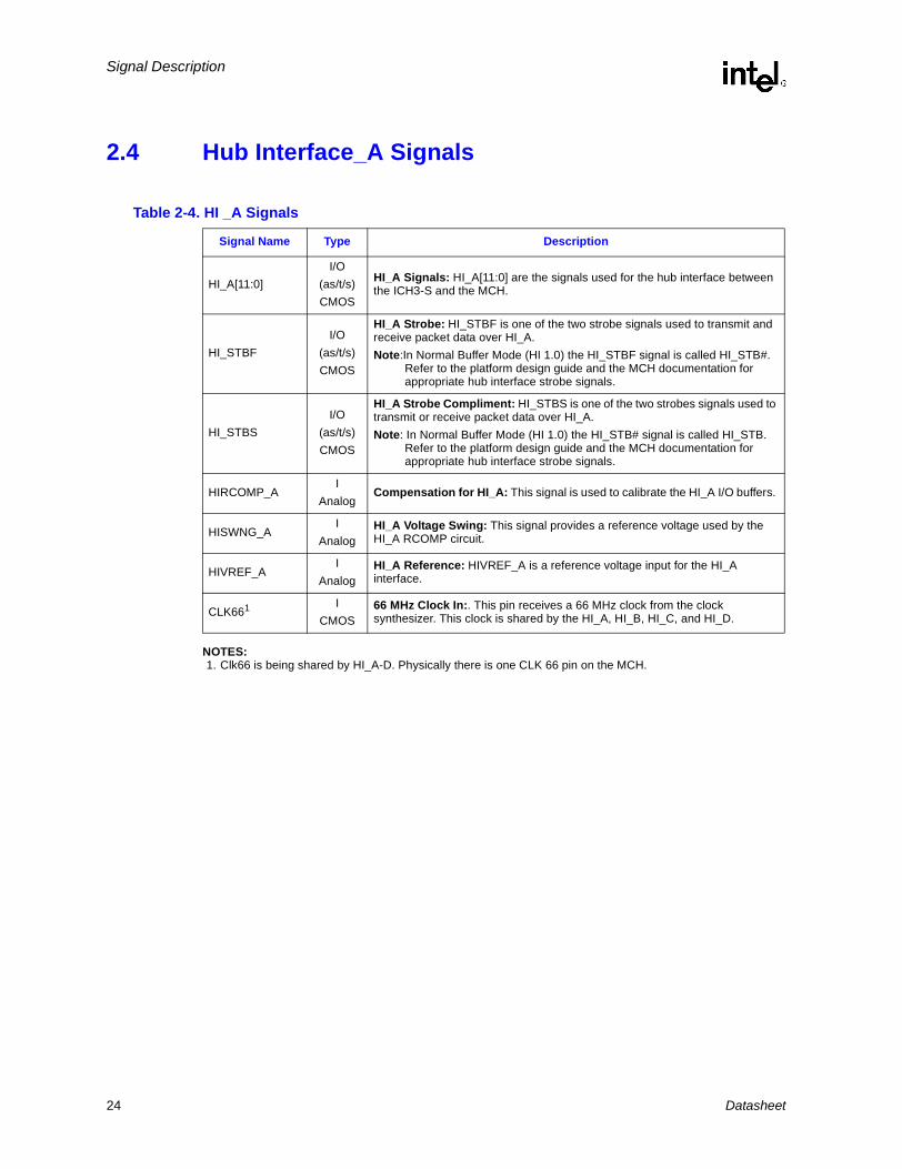
2.4 Hub Interface_A Signals
NOTES:1. Clk66 is being shared by HI_A-D. Physically there is one CLK 66 pin on the MCH.
Table 2-4. HI _A Signals
Signal Name Type Description
HI_A[11:0]I/O
(as/t/s)CMOS
HI_A Signals: HI_A[11:0] are the signals used for the hub interface between the ICH3-S and the MCH.
HI_STBFI/O
(as/t/s)CMOS
HI_A Strobe: HI_STBF is one of the two strobe signals used to transmit and receive packet data over HI_A.Note:In Normal Buffer Mode (HI 1.0) the HI_STBF signal is called HI_STB#.
Refer to the platform design guide and the MCH documentation for appropriate hub interface strobe signals.
HI_STBSI/O
(as/t/s)CMOS
HI_A Strobe Compliment: HI_STBS is one of the two strobes signals used to transmit or receive packet data over HI_A.Note: In Normal Buffer Mode (HI 1.0) the HI_STB# signal is called HI_STB.
Refer to the platform design guide and the MCH documentation for appropriate hub interface strobe signals.
HIRCOMP_AI
AnalogCompensation for HI_A: This signal is used to calibrate the HI_A I/O buffers.
HISWNG_AI
AnalogHI_A Voltage Swing: This signal provides a reference voltage used by the HI_A RCOMP circuit.
HIVREF_AI
AnalogHI_A Reference: HIVREF_A is a reference voltage input for the HI_A interface.
CLK661 ICMOS
66 MHz Clock In:. This pin receives a 66 MHz clock from the clock synthesizer. This clock is shared by the HI_A, HI_B, HI_C, and HI_D.
24 Datasheet

Signal Description
2.5 Hub Interface_B Signals1)
NOTES:1. Clk66 is being shared by HI_A-D. Physically there is one CLK 66 pin on the MCH.
Table 2-5. HI_B Signals
Signal Name Type Description
HI_B[21:20]I/O
(as/t/s)CMOS
HI_B Signals: HI_B[21:20] are the ECC signals used for connection between the 16-bit hub and the MCH.
HI_B[18:0]I/O
(as/t/s)CMOS
HI_B Signals: The HI_B[18:0] signals are used for connection between the 16-bit hub and the MCH.
PSTRBF_BI/O
(as/t/s)CMOS
HI_B Strobe First: PSTRBF_B is one of two strobes signal pairs used to transmit or receive lower 8-bit data over HI_B.
PSTRBS_BI/O
(as/t/s)CMOS
HI_B Strobe Second: PSTRBS_B is one of two strobes signal pairs used to transmit or receive lower 8-bit packet data over HI_B.
PUSTRBF_BI/O
(as/t/s)CMOS
HI_B Upper Strobe First: PUSTRBF_B is one of two strobes signal pairs used to transmit or receive upper 8-bit packet data over HI_B.
PUSTRBS_BI/O
(as/t/s)CMOS
HI_B Upper Strobe Second: PUSTRBS_B is one of two strobes signal pairs used to transmit or receive upper 8-bit packet data over HI_B.
HIRCOMP_BI/O
CMOSCompensation for HI_B: This signal is used to calibrate the HI_B I/O buffers.
HISWNG_BI
AnalogHI_B Voltage Swing: This signal provides a reference voltage used by the HI_B RCOMP circuit.
HIVREF_BI
AnalogHI_B Reference: HIVREF_B is a reference voltage input for the HI_B interface.
CLK661 ICMOS
66 MHz Clock In: This pin receives a 66 MHz clock from the clock synthesizer. This clock is shared by the HI_A, HI_B, HI_C and HI_D.
Datasheet 25

Signal Description
2.6 Hub Interface_C Signals
NOTES:1. Clk66 is being shared by HI_A-D. Physically there is one CLK 66 pin on the MCH.
Table 2-6. HI_C Signals
Signal Name Type Description
HI_C[21:20]I/O
(as/t/s)CMOS
HI_C Signals: HI_C[21:20] are the ECC signals used for connection between the 16-bit hub and the MCH.
HI_C[18:0]I/O
(as/t/s)CMOS
HI_C Signals: HI_C[18:0] are the signals used for the connection between the 16-bit hub and the MCH.
PSTRBF_CI/O
(as/t/s)CMOS
HI_C Strobe First: PSTRBF_C is one of two strobe signal pairs used to transmit or receive lower 8-bit data over HI_C.
PSTRBS_CI/O
(as/t/s)CMOS
HI_C Strobe second: PSTRBS_C is one of two strobe signals pairs used to transmit or receive lower 8-bit data over HI_C.
PUSTRBF_CI/O
(as/t/s)CMOS
HI_C Upper Strobe First: PUSTRBF_C is one of two strobe signals pairs used to transmit or receive upper 8-bit data over HI_C.
PUSTRBS_CI/O
(as/t/s)CMOS
HI_C Upper Strobe Second: PUSTRBS_C is one of two strobe signals pairs used to transmit or receive upper 8-bit data over HI_C.
HIRCOMP_CI/O
CMOSCompensation for HI_C: This signal is used to calibrate the HI_C I/O buffers.
HISWNG_CI
AnalogHI_C Voltage Swing: This signal provides a reference voltage used by the HI_C RCOMP circuit.
HIVREF_CI
AnalogHI_C Reference: HIVREF_C is a reference voltage input for the HI_C interface.
CLK661 ICMOS
66 MHz Clock In:. This pin receives a 66 MHz clock from the clock synthesizer. This clock is shared by the HI_A, HI_B, HI_C and HI_D.
26 Datasheet

Signal Description
2.7 Hub Interface_D Signals
NOTES:1. Clk66 is being shared by HI_A-D. Physically there is one CLK 66 pin on the MCH.
Table 2-7. HI_D Signals
Signal Name Type Description
HI_D[21:20]I/O
(as/t/s)CMOS
HI_D Signals: HI_D[21:20] are ECC signals used for connection between the 16-bit hub and the MCH.
HI_D[18:0]I/O
(as/t/s)CMOS
HI_D Signals: HI_D[18:0] are the signals used for the connection between the 16-bit hub and the MCH.
PSTRBF_DI/O
(as/t/s)CMOS
HI_D Strobe First: PSTRBF_D is one of two strobe signal pairs used to transmit or receive lower 8-bit data over HI_D.
PSTRBS_DI/O
(as/t/s)CMOS
HI_D Strobe Second: PSTRBS_D is one of two strobe signal pairs used to transmit or receive lower 8-bit data over HI_D.
PUSTRF_DI/O
(as/t/s)CMOS
HI_D Upper Strobe First: PUSTRF_D is one of two strobe signal pairs used to transmit or receive upper 8-bit data over HI_D.
PUSTRS_DI/O
(as/t/s)CMOS
HI_D Upper Strobe Second: PUSTRS_D is one of two strobe signal pairs used to transmit or receive upper 8-bit data over HI_D.
HIRCOMP_DI/O
CMOSCompensation for HI_D: This signal is used to calibrate the HI_D I/O buffers.
HISWNG_DI
AnalogHI_D Voltage Swing: This signal provides a reference voltage used by the HI_DRCOMP circuit.
HIVREF_DI
AnalogHI_D Reference: HIVREF_D is the reference voltage input for the HI_D interface.
CLK661 ICMOS
66 MHz Clock In:. This pin receives a 66 MHz clock from the clock synthesizer. This clock is shared by the HI_A, HI_B, HI_C and HI_D.
Datasheet 27

Signal Description
2.8 Clocks, Reset, Power, and Miscellaneous SignalsThe voltage reference pins are described in the signal description sections for the associated interface.
2.9 Pin States During and After Reset This section provides the signal states during reset (assertion of RSTIN#) and immediately following reset (deassertion of RSTIN#).
Table 2-8. Clocks, Reset, Power, and Miscellaneous Signals
Signal Name Type Description
RSTIN#I
CMOSReset In: When asserted, RSTIN# asynchronously resets the MCH logic. This signal is connected to the PCIRST# output of the ICH3-S.
XORMODE#I
CMOSTest Input: When XORMODE# is asserted, the MCH places all outputs in XOR mode for board-level testing.
PWRGOOD I Power Good: This signal resets the MCH component, including “sticky” logic. It is driven by external logic to indicate all power rails are present.
SMB_CLK I/O SMBus Clock: This is the clock pin for the SMBus interface.
SMB_DATA I/O SMBus Data: This is the data pin for the SMBus interface.
VCC1_2 Power: These pins are 1.2 V power input pins for HI_A–D, and the MCH core.
VCCA1_2 Power: These pins are 1.2 V analog power input pins.
VCCAHI1_2 Power: This pin is a 1.2 V analog power input pin.
VCCACPU1_2 Power: This pin is a 1.2 V analog power input pin.
VCC_CPU Power: For the system bus interface.
VCC2_5 Power: These pins are 2.5 V power input pins for DDR.
VSS Ground: Ground pin.
Legend Interpretation
Drive Strong drive (to normal value supplied by core logic, if not otherwise stated
TERM Normal termination devices on
LV Low voltage
HV High voltage
IN Input buffer enabled
ISO Isolate inputs in inactive states
TRI Tri-state
PU Weak pull-up
PD Weak pull-down
28 Datasheet

Signal Description
Signal NameState During
RSTIN# Assertion
State After RSTIN#
Deassertion
System Bus Interface
CPURST# DRIVE LV TERM HV (after 1ms)
HA[35:3]# TERM HV 1 TERM HV 2
HADSTB[1:0]# TERM HV TERM HV
AP[1:0]# TERM HV TERM HV
HD[63:0]# TERM HV TERM HV
HDSTBp[3:0]# TERM HV TERM HV
HDSTBn[3:0]# TERM HV TERM HV
DEP[3:0]# TERM HV TERM HV
DBI[3:0]# TERM HV TERM HV
ADS# TERM HV TERM HV
BNR# TERM HV TERM HV
BPRI# TERM HV TERM HV
DBSY# TERM HV TERM HV
DEFER# TERM HV TERM HV
DRDY# TERM HV TERM HV
HIT# TERM HV TERM HV
HITM# TERM HV TERM HV
HLOCK# TERM HV TERM HV
HREQ[4:0]# TERM HV TERM HV
HTRDY# TERM HV TERM HV
RS[2:0]# TERM HV TERM HV
RSP# TERM HV TERM HV
BERR# TERM HV TERM HV
BREQ0# TERM HV DRIVE LV 3
HDVREF[3:0] IN IN
HAVREF[1:0] IN IN
HCCVREF IN IN
HXRCOMP TRI TRI after RCOMP
HYRCOMP TRI TRI after RCOMP
HXSWNG IN IN
HYSWNG IN IN
DDR Channel A Interface
CB_A[7:0] TRI TRI
DQ_A[63:0] TRI TRI
DQS_A[17:0] TRI TRI
CMDCLK_A[3:0] LV Starts to toggle
CMDCLK_A[3:0]# LV Starts to toggle
MA_A[12:0] Note 4 Note 4
BA_A[1:0] Note 4 Note 4
RAS_A# LV LV
CAS_A# HV HV
WE_A# HV HV
CS_A[7:0]# HV HV
CKE_A LV Note 6
RCVENIN_A# IN IN
RCVENOUT_A# HV HV
DDR Channel B Interface
CB_B[7:0] TRI TRI
DQ_B[63:0] TRI TRI
DQS_B[17:0] TRI TRI
CMDCLK_B[3:0] LV Starts to toggle
CMDCLK_B[3:0]# LV Starts to toggle
MA_B[12:0] Note 4 Note 4
BA_B[1:0] Note 4 Note 4
RAS_B# LV LV
CAS_B# HV HV
WE_B# HV HV
CS_B[7:0]# HV HV
CKE_B LV Note 6
RCVENIN_B# IN IN
RCVENOUT_B# HV HV
Signal NameState During
RSTIN# Assertion
State After RSTIN#
Deassertion
Datasheet 29

Signal Description
NOTES:1. DRIVE LV if POC or Straps are set2. Any signals driven LV from POC Register go to
TERM HV two clocks after CPURST# deasserts3. Drive LV and hold until two clocks after CPURST#
is deasserted, and then TERM HV. 4. Active 0 or 1, either is ok5. Weak PU for Swizzle; Weak PD for non-Swizzle6. Remains low and is asserted after 256 clocks
Hub Interface_A
HI7_A Weak PU TERM LV
HI_A[11:8,6:0] Weak PD TERM LV
HI_STBF Weak PD TERM LV
HI_STBS Weak PD TERM LV
HIRCOMP_A TRI TRI after RCOMP
HIVREF_A IN IN
HISWNG_A IN IN
Hub Interface_B–D
HI_x[21:17,15:0] Weak PD TERM LV
HI16_x Note 5 TERM LV
PSTRBF_x, PUSTRBF_x Weak PD TERM LV
PSTRBS_x, PUSTRBS_x Weak PD TERM LV
HIRCOMP_x TRI TRI after RCOMP
HIVREF_x IN IN
HISWNG_x IN IN
Signal NameState During
RSTIN# Assertion
State After RSTIN#
Deassertion
Clocks and Miscellaneous
HCLKIN[N:P] IN IN
CLK66 IN IN
RSTIN# IN IN
XORMODE# IN IN
PWRGOOD IN IN
Signal NameState During
RSTIN# Assertion
State After RSTIN#
Deassertion
30 Datasheet

Register Description
Register Description 3
The MCH contains two sets of software accessible registers, accessed via the host processor I/O address space:
• Control registers – These registers are I/O mapped into the processor I/O space, which control access to PCI configuration space (see Section 3.5, “I/O Mapped Registers” on page 3-35)
• Internal configuration registers – These registers, which reside within the MCH, are partitioned into multiple logical device register sets (“logical” since they reside within a single physical device). One register set is dedicated to Host-HI Bridge functionality (controls PCI_A, DRAM configuration, other chipset operating parameters, and optional features). Other sets of registers map to HI_B, HI_C and HI_D.
The MCH supports PCI configuration space accesses using the mechanism denoted as Configuration Mechanism #1 in the PCI specification.
The MCH internal registers (I/O mapped and configuration registers) are accessible by the host. The registers can be accessed as Byte (8-bit), Word (16-bit), or DWord (32-bit) quantities, with the exception of the CONF_ADDR Register, which can only be accessed as a DWord. All multi-byte numeric fields use “little-endian” ordering (i.e., lower addresses contain the least significant parts of the field).
3.1 Register Terminology
Term Description
RO
Read Only. In some cases, If a register is read only, writes to this register location have no effect. However, in other cases, two separate registers are located at the same location where a read accesses one of the registers and a write accesses the other register. See the I/O and memory map tables for details.
WO
Write Only. In some cases, If a register is write only, reads to this register location have no effect. However, in other cases, two separate registers are located at the same location where a read accesses one of the registers and a write accesses the other register. See the I/O and memory map tables for details.
R/W Read/Write. A register with this attribute can be read and written.
R/WC Read/Write Clear. A register bit with this attribute can be read and written. However, a write of 1 clears (sets to 0) the corresponding bit and a write of 0 has no effect.
R/W/L Read/Write/Lock. A register with this attribute can be read, written and locked.
R/WO Read/Write Once. A register (bit) with this attribute can be written only once after power up. After the first write, the register (bit) becomes read only.
L Lock. A register bit with this attribute becomes read only after a lock bit is set.
Datasheet 31

Register Description
3.2 Platform ConfigurationThe MCH and the ICH3-S are physically connected by HI_A. From a configuration standpoint, HI_A is logically PCI bus 0. As a result, all devices internal to the MCH and ICH3-S appear to be on PCI bus 0. The system’s primary PCI expansion bus is physically attached to the ICH3-S and, from a configuration perspective appears to be a hierarchical PCI bus behind a PCI-to-PCI bridge and therefore has a programmable PCI Bus number.
Note: The primary PCI bus is referred to as PCI_A in this document and is not PCI bus 0 from a configuration standpoint.
The 16-bit hub interface ports appear to system software to be real PCI buses behind PCI-to-PCI bridges resident as devices on PCI bus 0.
The MCH decodes multiple PCI Device numbers. The configuration registers for the devices are mapped as devices residing on PCI bus 0. Each Device Number may contain multiple functions.
• Device 0: Host-HI_A Bridge/DRAM Controller. Logically this appears as a PCI device residing on PCI bus 0. Physically Device 0 contains the standard PCI bridge registers, DRAM registers, configuration for HI_A, and other MCH specific registers.
• Device 2: Host-HI_B Bridge. Logically this bridge appears to be a PCI-to-PCI bridge device residing on PCI bus 0. Physically, Device 2 contains the standard PCI bridge registers and configuration registers for HI_B.
• Device 3: Host-HI_C Bridge. Logically this bridge appears to be a PCI-to-PCI bridge device residing on PCI bus 0. Physically, Device 3 contains the standard PCI bridge registers and configuration registers for HI_C.
• Device 4: Host-HI_D Bridge. Logically this bridge appears to be a PCI-to-PCI bridge device residing on PCI bus 0. Physically, Device 4 contains the standard PCI bridge registers and configuration registers for HI_D.
Reserved Bits
Some of the MCH registers described in this chapter contain reserved bits. These bits are labeled Reserved (Rsvd). Software must deal correctly with fields that are reserved. On reads, software must use appropriate masks to extract the defined bits and not rely on reserved bits being any particular value. On writes, software must ensure that the values of reserved bit positions are preserved. That is, the values of reserved bit positions must first be read, merged with the new values for other bit positions and then written back. Note the software does not need to perform read, merge, and write operations for the configuration address register.
Reserved Registers
The MCH contains address locations in the configuration space of the Host-HI Bridge entity that are marked “Reserved”. Registers that are marked as “Reserved” must not be modified by system software. Writes to “Reserved” registers may cause system failure. Reads to “Reserved” registers may return a non-zero value.
Default Value upon Reset
Upon a Reset, the MCH sets its internal configuration registers to predetermined default states. At reset, some register values are determined by external strapping options. A register’s default value represents the minimum functionality feature set required to successfully bring up the system. Hence, it does not represent the optimal system configuration. It is the responsibility of the system initialization software (usually BIOS) to properly determine the DRAM configurations, operating parameters and optional system features that are applicable, and to program the MCH registers accordingly.
Term Description
32 Datasheet

Register Description
Table 3-1 shows the Device # assignment for the various internal MCH devices. All of these devices are on Bus #0.
3.3 General Routing Configuration AccessesThe MCH supports up to four hub interfaces: HI_A, HI_B, HI_C, and HI_D. PCI configuration cycles are selectively routed to one of these interfaces. The MCH is responsible for routing PCI configuration cycles to the proper interface. PCI configuration cycles to ICH3-S internal devices and Primary PCI (including downstream devices) are routed to the ICH3-S via HI_A. PCI configuration cycles to any of the 16-bit hub interfaces are routed to HI_B, HI_C, and HI_D. Routing of configuration accesses to HI_B, HI_C, and HI_D is controlled via the standard PCI-PCI bridge mechanism using information contained within the primary bus number, the secondary bus number, and the subordinate bus number registers of the corresponding PCI-PCI bridge device.
A detailed description of the mechanism for translating processor I/O bus cycles to configuration cycles on one of the buses is described below.
Note: The MCH supports a variety of connectivity options. When any of the MCH’s interfaces are disabled, the associated interface’s device registers are not visible. Configuration cycles to these registers will return all 1s for a read and master abort for a write.
3.3.1 Standard PCI Configuration MechanismThe PCI bus defines a slot-based configuration space that allows each device to contain up to eight functions; each function contains up to 256, 8-bit configuration registers. The PCI specification defines two bus cycles to access the PCI configuration space: Configuration Read and Configuration Write. Memory and I/O spaces are supported directly by the processor. Configuration space is supported by a mapping mechanism implemented within the MCH. The PCI specification defines two mechanisms to access configuration space, Mechanism 1 and Mechanism 2. The MCH supports only Mechanism 1.
The configuration access mechanism makes use of the CONF_ADDR Register and CONF_DATA Register. To reference a configuration register a DWord I/O write cycle is used to place a value into CONF_ADDR that specifies the PCI bus, the device on that bus, the function within the device, and a specific configuration register of the device function being accessed. CONF_ADDR[31] must be 1 to enable a configuration cycle. CONF_DATA then becomes a window into the four
Table 3-1. Intel® E7500 MCH Logical Configuration Resources
Intel® MCH Function Device #, Function #
DRAM Controller (8 bit HI_A) Device 0, Function 0
DRAM Controller Error Reporting (8 bit HI_A) Device 0, Function 1
Host-to-HI_B Bridge Controller (16 bit PCI2PCI) Device 2, Function 0
Host-to-HI_B Bridge Error Reporting (16 bit PCI2PCI) Device 2, Function 1
Host-to-HI_C Bridge Controller (16 bit PCI2PCI) Device 3, Function 0
Host-to-HI_C Bridge Error Reporting (16 bit PCI2PCI) Device 3, Function 1
Host-to-HI_D Bridge Controller (16 bit PCI2PCI) Device 4, Function 0
Host-to-HI_D Bridge Error Reporting (16 bit PCI2PCI) Device 4, Function 1
Datasheet 33

Register Description
bytes of configuration space specified by the contents of CONF_ADDR. Any read or write to CONF_DATA results in the MCH translating the CONF_ADDR into the appropriate configuration cycle.
The MCH is responsible for translating and routing the processor’s I/O accesses to the CONF_ADDR and CONF_DATA Registers to internal MCH configuration registers for HI_A, HI_B, HI_C, and HI_D.
3.3.2 Logical PCI Bus 0 Configuration MechanismThe MCH decodes the Bus Number (bits 23:16) and the Device Number fields of the CONF_ADDR Register. When the Bus Number field of CONF_ADDR is 0, the configuration cycle is targeting a PCI bus 0 device.
• The Host-HI_A bridge entity within the MCH is hardwired as Device 0 on PCI Bus 0.
• The Host-HI_B bridge entity within the MCH is hardwired as Device 2 on PCI Bus 0.
• The Host-HI_C bridge entity within the MCH is hardwired as Device 3 on PCI Bus 0.
• The Host-HI_D bridge entity within the MCH is hardwired as Device 4 on PCI Bus 0.
Configuration cycles to any of the MCH’s enabled internal devices are confined to the MCH and not sent over HI_A. Accesses to devices 8 to 31 are forwarded over HI_A as Type 0. The ICH3-S decodes the Type 0 access and generates a configuration access to the selected internal device.
3.3.3 Primary PCI Downstream Configuration MechanismWhen the Bus Number in the CONF_ADDR is non-zero, and does not lie between the Secondary Bus Number registers and the Subordinate Bus Number registers for one of the HI_16, the MCH will generate a type 1 HI_A configuration cycle.
When the cycle is forwarded to the ICH3-S via HI_A, the ICH3-S compares the non-zero Bus Number with the Secondary Bus Number and Subordinate Bus Number registers of its PCI- PCI bridges to determine if the configuration cycle is meant for Primary PCI, or a downstream PCI bus.
3.3.4 HI_B, HI_C, HI_D Bus Configuration MechanismFrom the chipset configuration perspective, HI_B, HI_C and HI_D are seen as PCI bus interfaces residing on a Secondary Bus side of the “virtual” PCI-PCI bridges referred to as the MCH Host-HI_B, HI_C and HI_D bridge.
Note: There is no requirement that the secondary and subordinate bus number values from one Hub Interface be contiguous with any other Hub Interfaces. It is possible that HI_B will decode buses 2 through 5, HI_C will decode buses 8 through 12, and HI_D will decode buses 13 through 15. In this case there is a gap where buses 6 and 7 are subtractively decoded to HI_A.
When the bus number is non-zero, greater than the value programmed into the Secondary Bus Number Register, and less than or equal to the value programmed into the corresponding Subordinate Bus Number Register, the configuration cycle is targeting a PCI bus downstream of the targeted hub interface. The MCH generates a Type 1configuration cycle on the appropriate hub interface.
34 Datasheet

Register Description
3.4 Sticky RegistersCertain registers in the MCH are sticky through a hard-reset. They will only be reset on a power-good reset. These registers in general are the error logging registers and a few special cases. The error command registers are not sticky. The following registers are sticky:
• Device 0, Function 1 error registers
• Device 2, Function 1 error registers
• Device 3, Function 1 error registers
• Device 4, Function 1 error registers
• Others that are determined to need to hold state through reset for function or test purposes
3.5 I/O Mapped RegistersThe MCH contains two registers that reside in the processor I/O address space; the Configuration Address (CONF_ADDR) Register and the Configuration Data (CONF_DATA) Register. The Configuration Address Register enables/disables the configuration space and determines what portion of configuration space is visible through the Configuration Data window.
3.5.1 CONF_ADDR—Configuration Address RegisterI/O Address: 0CF8h Accessed as a DWordDefault Value: 00000000hAccess: R/W Size: 32 bits
CONF_ADDR is a 32-bit register that can be accessed only as a DWord. A Byte or Word reference will pass through the Configuration Address Register and HI_A onto the PCI_A bus as an I/O cycle. The CONF_ADDR Register contains the Bus Number, Device Number, Function Number, and Register Number that a subsequent configuration access is intended.
Bit Descriptions
31Configuration Enable (CFGE). 0 = Disable1 = Enable
30:24 Reserved (These bits are read only and have a value of 0).
23:16 Bus Number. Contains the bus number being targeted by the config cycle.
15:11 Device Number. Selects one of the 32 possible devices per bus.
10:8 Function Number. Selects one of 8 possible functions within a device.
7:2Register Number: This field selects one register within a particular Bus, Device, and Function as specified by the other fields in the Configuration Address Register. This field is mapped to A[7:2] during HI_A–D Configuration cycles.
1:0 Reserved.
Datasheet 35

Register Description
3.5.2 CONF_DATA—Configuration Data RegisterI/O Address: 0CFChDefault Value: 00000000hAccess: Read/Write Size: 32 bits
CONF_DATA is a 32-bit read/write window into configuration space. The portion of configuration space that is referenced by CONF_DATA is determined by the contents of CONF_ADDR.
Bit Descriptions
31:0 Configuration Data Window (CDW). If bit 31 of CONF_ADDR is 1, any I/O access to the CONF_DATA register are mapped to configuration space using the contents of CONF_ADDR.
36 Datasheet

Register Description
3.6 DRAM Controller Registers (Device 0, Function 0)The DRAM Controller registers are in Device 0 (D0), Function 0 (F0). Table 3-2 provides the register address map for this device, function.
Warning: Address locations that are not listed the table are considered reserved register locations. Writes to “Reserved” registers may cause system failure. Reads to “Reserved” registers may return a non-zero value.
Table 3-2. DRAM Controller Register Map (HI_A—D0:F0)Offset Mnemonic Register Name Default Type
00–01h VID Vendor ID 8086h RO
02–03h DID Device ID 2540h RO
04–05h PCICMD PCI Command 0006h RO, R/W
06–07h PCISTS PCI Status 0090h RO, R/WC
08h RID Revision ID 02h RO
0Ah SUBC Sub Class Code 00h RO
0Bh BCC Base Class Code 06h RO
0Dh MLT Master Latency Timer 00h —
0Eh HDR Header Type 00h RO
2C–2Dh SVID Subsystem Vendor Identification 0000h R/WO
2E–2Fh SID Subsystem Identification 0000h R/WO
50–51h MCHCFG MCH Configuration 0004h R/W
52–53h MCHCFGNS MCH Memory Scrub and Init Configuration 0000h RO, R/W
58h FDHC Fixed DRAM Hole Control 00h R/W
59–5Fh PAM[0:6] Programmable Attribute Map (7 registers) 00h R/W
60–6Fh DRB DRAM Row Boundary 00h R/W
70–77h DRA DRAM Row Attribute 00h R/W
78–7Bh DRT DRAM Timing 00000010h R/W
7C–7Fh DRC DRAM Controller Mode 00440009h R/W
8Ch CLOCK_DIS CK/CK# Disable 00h R/W
9Dh SMRAM System Management RAM Control 02h RO, R/W, L
9Eh ESMRAMC Extended System Management RAM Control 38h R/W, R/WC,
R/W/L
C4–C5h TOLM Top of Low Memory 0800h R/W
C6–C7h REMAPBASE Remap Base Address 03FFh R/W
C8–C8h REMAPLIMIT Remap Limit Address 0000h R/W
DE–DFh SKPD Scratchpad Data 0000h R/W
E0–E1h DVNP Device Not Present 1D1Fh R/W
Datasheet 37

Register Description
3.6.1 VID—Vendor Identification Register (D0:F0)
The VID Register contains the vendor identification number. This 16-bit register combined with the Device Identification Register uniquely identify any PCI device.
3.6.2 DID—Device Identification Register (D0:F0)
This 16-bit register combined with the Vendor Identification register uniquely identifies any PCI device.
Address Offset: 00–01hDefault: 8086hAccess: RO Size: 16 Bits
Bits Default, Access Description
15:08086h
ROVendor Identification (VID). This register field contains the PCI standard identification for Intel (VID=8086h).
Address Offset: 02–03hDefault: 2540hAccess: RO Size: 16 Bits
Bits Default, Access Description
15:02540h
RODevice Identification Number (DID). This is a 16-bit value assigned to the MCH Host-HI Bridge Function 0.
38 Datasheet

Register Description
3.6.3 PCICMD—PCI Command Register (D0:F0)
Since MCH Device 0 does not physically reside on a physical PCI bus portions of this register are not implemented.
Address Offset: O4–05hDefault: 0006hAccess: RO, R/W Size: 16 Bits
Bits Default, Access Description
15:10 00h Reserved
9 0bRO
Fast Back-to-Back Enable (FB2B). Hardwired to 0. This bit controls whether or not the master can do fast back-to-back writes. Since device 0 is strictly a target this bit is not implemented.
8 0b
R/W
SERR Enable (SERRE). This is a global enable bit for Device 0 SERR messaging. The MCH does not have an SERR signal. The MCH communicates the SERR condition by sending an SERR message over HI_A to the ICH3-S. 0 = Disable. SERR message is not generated by the MCH for Device 0. 1 = Enable. The MCH is enabled to generate SERR messages over HI_A for specific
Device 0 error conditions that are individually enabled in the ERRCMD register. The error status is reported in the ERRSTAT and PCISTS registers. When SERRE is cleared, the SERR message is not generated by the MCH for Device 0.
NOTE: This bit only controls SERR messaging for the Device 0. Devices 2–4 have their own SERR bits to control error reporting for error conditions occurring on their respective devices. The control bits are used in a logical OR configuration to enable the SERR HI message mechanism.
7 0bRO
Address/Data Stepping Enable (ADSTEP). Hardwired to 0. Address/data stepping is not implemented in the MCH.
6 0b
R/W
Parity Error Enable (PERRE). 0 = Disable. MCH takes no action when it detects a parity error on HI_A. 1 = Enable. MCH generates an SERR message over HI_A to the ICH3-S when an
address or data parity error is detected by the MCH on HI_A (DPE set in PCISTS).
5 0bRO
VGA Palette Snoop Enable (VGASNOOP). Hardwired to 0. The MCH does not implement this bit.
4 0bRO
Memory Write and Invalidate Enable (MWIE). Hardwired to 0. The MCH will never issue memory write and invalidate commands.
3 0bRO
Special Cycle Enable (SCE). Hardwired to 0. The MCH does not implement this bit.
2 1bRO
Bus Master Enable (BME). Hardwired to 1. The MCH is always enabled as a master on HI_A.
1 1bRO
Memory Access Enable (MAE). Hardwired to 1. The MCH always allows access to main memory.
0 0bRO
I/O Access Enable (IOAE). Hardwired to 0. This bit is not implemented in the MCH.
Datasheet 39

Register Description
3.6.4 PCISTS—PCI Status Register (D0:F0)
PCISTS is a 16-bit status register that reports the occurrence of error events on Device 0’s PCI interface. All other bits are Read Only. Since MCH Device 0 does not physically reside on a PCI bus, many of these bits are not implemented.
Note: Software must write a 1 to clear bits that are set.
Address Offset: 06–07hDefault: 0090hAccess: RO, R/WC Size: 16 Bits
Bits Default, Access Description
150b
R/WC
Detected Parity Error (DPE). 0 = No Parity error detected. 1 = MCH detected an address or data parity error on the HI_A interface.
140b
R/WC
Signaled System Error (SSE). 0 = No SERR generated by MCH Device 0. 1 = MCH Device 0 generates an SERR message over HI_A for any enabled Device 0
error condition. Device 0 error conditions are enabled in the PCICMD and ERRCMD Registers. Device 0 error flags are read/reset from the PCISTS or ERRSTAT Registers.
130bRO
Received Master Abort Status (RMAS). Hardwired to 0. The ICH3-S never sends a Master Abort completion.
120b
R/WC
Received Target Abort Status (RTAS). 0 = No received Target Abort generated by MCH.1 = MCH generated a HI_A request that received a Target Abort.
110bRO
Signaled Target Abort Status (STAS). Hardwired to 0. The MCH will not generate a Target Abort on HI_A. This bit is not implemented.
10:900bRO
DEVSEL Timing (DEVT). These bits are hardwired to 00. Device 0 does not physically connect to PCI_A. These bits are set to 00 (fast decode) so that optimum DEVSEL timing for PCI_A is not limited by the MCH.
80bRO
Master Data Parity Error Detected (DPD). Hardwired to 0. PERR signaling and messaging are not implemented by the MCH.
71bRO
Fast Back-to-Back (FB2B). Hardwired to 1. Device 0 does not physically connect to PCI_A. This bit is set to 1 (indicating fast back-to-back capability) so that the optimum setting for PCI_A is not limited by the MCH.
6:0 00h Reserved
40 Datasheet

Register Description
3.6.5 RID—Revision Identification Register (D0:F0)
This register contains the revision number of the MCH Device 0.
3.6.6 SUBC—Sub-Class Code Register (D0:F0)
This register contains the Sub-Class Code for the MCH Device 0.
3.6.7 BCC—Base Class Code Register (D0:F0)
This register contains the Base Class Code of the MCH Device 0.
Address Offset: 08hDefault: See table belowAccess: ROSize: 8 Bits
Bits Default, Access Description
7:0 00hRO
Revision Identification Number (RID). This is an 8-bit value that indicates the revision identification number for the MCH Device 0.02h = A2 stepping
Address Offset: 0AhDefault: 00hAccess: ROSize: 8 Bits
Bits Default, Access Description
7:0 00hRO
Sub-Class Code (SUBC). This is an 8-bit value that indicates the category of Bridge into which the MCH falls. 00h = Host bridge.
Address Offset: 0BhDefault: 06hAccess: RO Size: 8 Bits
Bits Default, Access Description
7:0 06hRO
Base Class Code (BASEC). This is an 8-bit value that indicates the Base Class Code for the MCH. 06h = Bridge device.
Datasheet 41

Register Description
3.6.8 MLT—Master Latency Timer Register (D0:F0)
Device 0 in the MCH is not a PCI master. Therefore, this register is not implemented.
3.6.9 HDR—Header Type Register (D0:F0)
This register identifies the header layout of the configuration space.
3.6.10 SVID—Subsystem Vendor Identification Register (D0:F0)
This value is used to identify the vendor of the subsystem.
Address Offset: 0DhDefault: 00hAccess: Reserved Size: 8 Bits
Bits Default, Access Description
7:0 00h Reserved
Address Offset: 0EhDefault: 00hAccess: RO Size: 8 Bits
Bits Default, Access Description
7:0 00hRO
PCI Header (HDR). This register returns 00 when Device 0, Function 1 is disabled. If Device 0, Function 1 is enabled via the DVNP Register, this register (HDR) returns 80h.
Address Offset: 2C–2DhDefault: 0000hAccess: R/WO Size: 16 Bits
Bits Default, Access Description
15:0 0000hR/WO
Subsystem Vendor ID (SUBVID). This field should be programmed during boot-up to indicate the vendor of the system board. After it has been written once, it becomes read only.
42 Datasheet

Register Description
3.6.11 SID—Subsystem Identification Register (D0:F0)
This value is used to identify a particular subsystem.
3.6.12 MCHCFG—MCH Configuration Register (D0:F0)
This register controls how the MCH tracks and routes system bus transactions.
Address Offset: 2E–2FhDefault: 0000hAccess: R/WO Size: 16 Bits
Bits Default, Access Description
15:0 0000hR/WO
Subsystem ID (SUBID). This field should be programmed during BIOS initialization. After it has been written once, it becomes read only.
Address Offset: 50–51hDefault: 0004hAccess: R/WSize: 16 Bits
Bits Default, Access Description
15:13 000b,R/W
Number of Stop Grant Cycles (NSG). These bits indicate the number of Stop Grant transactions expected on the system bus before a Stop Grant Acknowledge packet is sent to the ICH3-S. This field is programmed by the BIOS after it has enumerated the processors and before it has enabled Stop Clock generation in the ICH3-S. Once this field has been set, it should not be modified. 000 = HI_A Stop Grant generated after 1 Stop Grant001 = HI_A Stop Grant generated after 2 Stop Grant010 = HI_A Stop Grant generated after 3 Stop Grant011 = HI_A Stop Grant generated after 4 Stop GrantOthers = Reserved
12:6 000000b Reserved
Datasheet 43

Register Description
5 0b
R/W
MDA Present (MDAP). This bit works with the VGA Enable bits in the BCTRL Registers of devices 2–4 to control the routing of processor initiated transactions targeting MDA compatible I/O and memory address ranges. This bit should not be set if none of the VGA Enable bits are set. When none of the VGA enable bits are set, accesses to I/O address range x3BCh–x3BFh are forwarded to HI_A. When the VGA enable bit is not set, accesses to I/O address range x3BCh–x3BFh are treated just like any other I/O accesses. That is, the cycles are forwarded to HI_B–D if the address is within the corresponding IOBASE and IOLIMIT and ISA enable bit is not set; otherwise, they are forwarded to HI_A. MDA resources are defined as the following:Memory: 0B0000h – 0B7FFFhI/O: 3B4h, 3B5h, 3B8h, 3B9h, 3BAh, 3BFh,
(including ISA address aliases, A[15:10] are not used in decode)Any I/O reference that includes the I/O locations listed above, or their aliases, will be forwarded to the hub interface, even if the reference includes I/O locations not listed above.The following shows the behavior for all combinations of MDA and VGA:VGAMDABehavior 0 0 All References to MDA and VGA go to HI_A 0 1 Illegal Combination (DO NOT USE)1 0 All References to VGA go to device with VGA enable set. MDA-only references (I/
O address 3BFh and aliases) will go to HI_A.1 1 VGA References go to the hub interface that has its VGAEN bit set. MDA
References go to HI_A
40b
R/W
Throttled-Write Occurred. 0 =Writing a zero clears this bit.1 =This bit is set when a write is throttled. This bit is set when the maximum allowed
number of writes has been reached during a time-slice and there is at least one more write to be completed.
3 0b Reserved
2 0bRO
In-Order Queue Depth (IOQD). This bit reflects the value sampled on HA7# on the deassertion of the CPURST#. It indicates the depth of the processor bus in-order queue. 0 = When IOQD is set to 0 (HA7# is sampled asserted; i.e., 1; or an electrical low), the
depth of the IOQ is set to 1 (i.e., no pipelining support on the processor bus). HA7# may be driven low during CPURST# by an external source.
1 = When IOQD is set to 1 (HA7# sampled as 0; an electrical high), the depth of the processor bus in-order queue is configured to the maximum allowed by the processor protocol (i.e., 12).
1:0 00b Reserved
Bits Default, Access Description
44 Datasheet

Register Description
3.6.13 MCHCFGNS—MCH Memory Scrub and Initialization Configuration Register (D0:F0)
This register controls the mode and status of the DRAM memory scrubber.
Address Offset: 52–53hDefault: 0000hAccess: RO, R/WSize: 16 Bits
Bits Default, Access Description
15:4 000h Reserved
30bRO
Valid ECC Initialization Complete. BIOS should poll this bit after enabling auto-initialization to determine when all the ECC values have been written to DRAM.1 = The scrub unit sets this bit to 1 after it has completed placing valid ECC data in each
line of memory.
20b
R/W
Initialization/Scrub Mode Select. This bit determines if the MCH is initializing memory (with valid ECC data) or running standard memory scrubbing. In the Initialization Mode, the MCH issues memory writes as quickly as possible and places valid ECC in each memory location. In Scrubbing Mode, the MCH scrubs a memory location (read a memory line and correct any ECC errors) every 32,000 clocks. This scrubs an entire 16 GB memory array in approximately 1 day.0 = Valid ECC Init Mode1 = ECC Scrub ModeBIOS should set this bit to 0, enable scrubbing via bit 0, wait until bit 3 (Valid ECC Init Complete) is set, and set this bit to 1 (or disable scrubbing).
1 0b Reserved
00b
R/W
Memory Initialization/Scrub Enable. This bit enables Valid ECC Init Mode or ECC Scrub Mode depending on the value in bit 2 (Init/Scrub Mode Select).0 = Disable1 = Enable
Datasheet 45

Register Description
3.6.14 FDHC—Fixed DRAM Hole Control Register (D0:F0)
This 8-bit register controls a fixed DRAM hole from 15 MB –16 MB
Address Offset: 58hDefault: 00hSticky: NoAccess: R/WSize: 8 Bits
Bit Field Default and Access Description
7 0bRW
Hole Enable (HEN). This field enables a memory hole in DRAM space. The DRAM that lies "behind" this space is not remapped.0 =No memory hole1 =Memory hole from 15 MB to 16 MB. Accesses to this range will be sent to
HI_A.
6:0 00h Reserved
46 Datasheet

Register Description
3.6.15 PAM[0:6]—Programmable Attribute Map Registers (D0:F0)
The MCH allows programmable memory attributes on 13 legacy memory segments of various sizes in the 640 KB to 1 MB address range. Seven Programmable Attribute Map (PAM) Registers support these features. However, not all seven of these registers are identical. PAM 0 controls only one segment (high), while PAM 1:6 controls two segments (high and low) each. Cacheability of these areas is controlled via the MTRR Registers in the processor. Two bits are used to specify memory attributes for each memory segment. These bits only apply to host initiator access to the PAM areas. The MCH forwards to main memory any Hub Interface_A–D initiated accesses to the PAM areas. At the time that hub interface accesses to the PAM region may occur, the targeted PAM segment must be programmed to be both readable and writeable. It is illegal to issue a hub initiated transaction to a PAM region with the associated PAM register not set to 11. Each of these regions has a 2-bit field. The two bits that control each region have the same encoding.
As an example, consider BIOS that is implemented on the expansion bus. During the initialization process, BIOS can be shadowed in main memory to increase the system performance. When BIOS is shadowed in main memory, it should be copied to the same address location. To shadow the BIOS, the attributes for that address range should be set to write only. The BIOS is shadowed by first doing a read of that address. This read is forwarded to the expansion bus. The host then does a write of the same address, which is directed to main memory. After the BIOS is shadowed, the attributes for that memory area are set to read only so that all writes are forwarded to the expansion bus. Table 3-3and Figure 3-1 show the PAM Registers and the associated attribute bits:
Address Offset: 59–5Fh (PAM0–PAM6)Default Value: 00hAccess: R/WSize: 8 bits each
Bits Default, Access Description
7:6 00b Reserved
5:400bR/W
Attribute Register (HIENABLE). This field controls the steering of read and write cycles that address the BIOS.00 = DRAM Disabled - All accesses are directed to HI_A01 = Read Only - All Reads are serviced by DRAM. All Writes are forwarded to HI_A.10 = Write Only - All writes are sent to DRAM. Reads are serviced by HI_A.11 = Normal DRAM operation - All reads and writes are serviced by DRAM
3:2 0h Reserved
1:000bR/W
Attribute Register (LOENABLE). This field controls the steering of read and write cycles that address the BIOS.00 =DRAM Disabled - All accesses are directed to HI_A01 =Read Only - All Reads are serviced by DRAM. All Writes are forwarded to HI_A.10 =Write Only - All writes are sent to DRAM. Reads are serviced by HI_A.1 1 =Normal DRAM operation - All reads and writes are serviced by DRAM
NOTE: The LO Segment for PAM0 is reserved as shown in Figure 3-1.
Datasheet 47

Register Description
Figure 3-1. PAM Registers
Table 3-3. PAM Associated Attribute Bits
PAM Reg Attribute Bits Memory Segment Comments Offset
PAM0 3:0, 7:6 Reserved — — 59h
PAM0 5:4 R R WE RE 0F0000h–0FFFFFh BIOS Area 59h
PAM1 3:2, 7:6 — — — — — Reserved 5Ah
PAM1 1:0 R R WE RE 0C0000h–0C3FFFh BIOS Area 5Ah
PAM1 5:4 R R WE RE 0C4000h–0C7FFFh BIOS Area 5Ah
PAM2 3:2, 7:6 — — — — — Reserved 5Bh
PAM2 1:0 R R WE RE 0C8000h–0CBFFFh BIOS Area 5Bh
PAM2 5:4 R R WE RE 0CC000h–0CFFFFh BIOS Area 5Bh
PAM3 3:2, 7:6 — — — — — Reserved 5Ch
PAM3 1:0 R R WE RE 0D0000h–0D3FFFh BIOS Area 5Ch
PAM3 5:4 R R WE RE 0D4000h–0D7FFFh BIOS Area 5Ch
PAM4 3:2, 7:6 — — — — — Reserved 5Dh
PAM4 1:0 R R WE RE 0D8000h–0DBFFFh BIOS Area 5Dh
PAM4 5:4 R R WE RE 0DC000h–0DFFFFh BIOS Area 5Dh
PAM5 3:2, 7:6 — — — — — Reserved 5Eh
PAM5 1:0 R R WE RE 0E0000h–0E3FFFh BIOS Extension 5Eh
PAM5 5:4 R R WE RE 0E4000h–0E7FFFh BIOS Extension 5Eh
PAM6 3:2, 7:6 — — — — — Reserved 5Fh
PAM6 1:0 R R WE RE 0E8000h–0EBFFFh BIOS Extension 5Fh
PAM6 5:4 R R WE RE 0EC000h–0EFFFFh BIOS Extension 5Fh
PAM6 5Fh
PAM1PAM2PAM3PAM4PAM5
5Ah5B h5C h5D h5Eh
O ffset
W ERRRER W E RER
7 0123456
Reserved
Reserved
W rite Enable (R /W )1 = Enable0 = D isable
Read Enable (R /W )1 = Enable0 = D isable Reserved
Reserved
W rite Enable (R /W )1 = Enable0 = D isable
R ead Enable (R /W )1 = Enab le0 = D isable
59hPAM0
H I Segm ent LO Segm ent
Reserved
48 Datasheet

Register Description
3.6.16 DRB—DRAM Row Boundary Register (D0:F0)
The DRAM Row Boundary Register defines the upper boundary address of each DRAM row with a granularity of 64 MB. A row is 144 bits wide (72 bits per channel). Each row has its own single-byte DRB Register. For example, a value of 1 in DRB0 indicates that 64 MB of DRAM has been populated in the first row.
Note: The MCH DRAM Row Boundary Registers (DRB Registers) are 8-bits wide, and define the upper boundary address for each DRAM row with a granularity of 64 MB. The DRB Registers are cumulative; therefore, DRB7 will contain the total memory contained in all eight DRAM rows. By this definition, the system is only allowed to report 16 GB–64 MB of memory populated.
Row 0 = 60hRow 1 = 61hRow 2 = 62hRow 3 = 63hRow 4 = 64hRow 5 = 65hRow 6 = 66hRow 7 = 67h68h to 6Fh are reserved
DRB0 = Total memory in row 0 (in 64 MB increments)
DRB1 = Total memory in row 0 + row 1 (in 64 MB increments)
DRB3 = Total memory in row 0 + row 1 + row 2 + row 3 (in 64 MB increments)
The row referred to by this register is defined by the DIMM chip select used. Double-sided DIMMs use both Row 0 and Row 1 (for CS0# and CS1#), even though there is one physical slot for the DIMM. Single-sided DIMMs use only the even row number, since single-sided DIMMs only support CS0#. For single-sided DIMMs, the value BIOS places in the odd row should equal the same value as what was placed in the even row field. A row is defined as 128-bit (144 bit with ECC) wide interface consisting of two identical DIMMs.
Address Offset: 60–6FhDefault: 00hAccess: R/W Size: 8 Bits
Bits Default, Access Description
7:0 00hR/W
DRAM Row Boundary Address. This 8-bit value defines the upper and lower addresses for each row of DRAM. This 8-bit value is compared against a set of address lines to determine the upper address limit of a particular row.
Datasheet 49

Register Description
3.6.17 DRA—DRAM Row Attribute Register (D0:F0)
The DRAM Row Attribute Register defines the page sizes to be used for each row of memory. Each nibble of information in the DRA registers describes the page size and device width of a row. For this register, a row is defined by the chip select used by the DIMM, so that a double-sided DIMM would have both an even and an odd entry. For single-sided DIMMs, only the even side is used.
Row 0, 1 = 70hRow 2, 3 = 71hRow 4, 5 = 72hRow 6, 7 = 73h
Address Offset: 70–77hDefault: R/WSize: 8 BitsDefault: 00h
Bits Default, Access Description
7 0b
R/W
Device Width for Odd-numbered Row. This bit defines whether the DDR-SDRAM devices populated in this row are 4 bits wide (x4) or 8 bits wide.0 =8 bits wide.1 =4 bits wide (x4).
6:4 000bR/W
Row Attribute for Odd-numbered Row. This 3-bit field defines the page size of the corresponding row. 010 = 8 KB011 = 16 KB100 = 32 KB101 = 64 KBOthers = Reserved
3 0b
R/W
Device Width for Even-numbered Row. This bit defines whether the DDR-SDRAM devices populated in this row are 4 bits wide (x4) or 8 bits wide.0 =8 bits wide.1 =4 bits wide (x4).
2:0 000bR/W
Row Attribute for Even-numbered Row. This 3-bit field defines the page size of the corresponding row. 010 = 8 KB011 = 16 KB100 = 32 KB101 = 64 KBOthers = Reserved
50 Datasheet

Register Description
3.6.18 DRT—DRAM Timing Register (D0:F0)
This register controls the timing of the DRAM Interface.
Address Offset: 78–7BhAccess: R/WSize: 32 BitsDefault: 00000010h
Bits Default, Access Description
31:30 00b Reserved
290b
R/W
Back to Back Write-Read Turn Around. This field determines the minimum number of CMDCLK (command clocks, at 100 MHz) between Write-Read commands. It applies to WR-RD pairs to different rows. The WR-RD pair to the same row has sufficient turnaround due to the tWTR timing parameter. The purpose of this bit is to control the turnaround time on the DQ bus.0 = 3 clocks between WR-RD commands (2 turnaround clocks on DQ)1 = 2 clocks between WR-RD commands (1 turnaround clock on DQ)
280b
R/W
Back to Back Read-Write Turn Around. This field determines the minimum number of CMDCLK (command clocks, at 100 MHz) between Read-Write commands. It applies to RD-WR pairs to any destination, in same or different rows. The purpose of this bit is to control the turnaround time on the DQ bus.0 = 5 clocks between RD-WR commands (2 turnaround clocks on DQ)1 = 4 clocks between RD-WR commands (1 turnaround clock on DQ)
270b
R/W
Back to Back Read Turn Around. This field determines the minimum number of CMDCLK (command clocks, at 100 MHz) between two reads destined to different rows. The purpose of this bit is to control the turnaround time on the DQ bus.0 = 4 clocks between RD commands to different rows (2 turnaround clocks on DQ)1 = 3 clocks between RD commands to different rows (1 turnaround clock on DQ)
26:24000bR/W
Read Delay (tRD). This field controls the number of 100 MHz clocks elapsed from the Read Command latched on the system bus until the returned data is set to be driven on the system bus. The following tRD values are supported.000 = 7 clocks001 = 6 clocks010 = 5 clocksOthers = Reserved
23:11 00000b Reserved
10:900bR/W
Activate to Precharge delay (tRAS). This bit controls the number of DRAM clocks for tRAS.00 = 7 Clocks01 = 6 Clocks 10 = 5 Clocks11 = Reserved
8:6 0000b Reserved
5:401bR/W
CAS# Latency (tCL). The number of clocks between the rising edge used by DRAM to sample the Read Command and the rising edge used by the DRAM to drive read data.00 = 2.5 Clocks01 = 2 Clocks10 = 1.5 Clocks11 = Reserved
Datasheet 51

Register Description
3.6.19 DRC—DRAM Controller Mode Register (D0:F0)
This register controls the mode of the DRAM Controller.
30b
R/W
Write RAS# to CAS# Delay (tRCD). This bit controls the number of clocks inserted between a row activate command and write command to that row.0 = 3 DRAM Clocks1 = 2 DRAM Clocks
2 0b Reserved
10b
R/W
Read RAS# to CAS# Delay (tRCD). This bit controls the number of clocks inserted between a row activate command and a read command to that row.0 = 3 DRAM Clocks1 = 2 DRAM Clocks
00b
R/W
DRAM RAS# Precharge (tRP). This bit controls the number of clocks that are inserted between a row precharge command and an activate command to the same row.0 = 3 DRAM Clocks1 = 2 DRAM Clocks
Address Offset: 7C–7FhDefault: 0044_0009hAccess: R/WSize: 32 Bits
Bits Default, Access Description
Bits Default, Access Description
31:30 00b Reserved
29 0b
R/W
Initialization Complete (IC). This bit is used for communicating the software state between the memory controller and the BIOS. It indicates that the DRAM interface has been initialized. This bit must be set and the refresh mode select (DRC[9:8]) must be set to enable refresh. If this bit is clear, no refresh will occur regardless of the RMS (DRC[9:8]) setting.
28:22 00h Reserved
21:20 00bR/W
DRAM Data Integrity Mode (DDIM). These bits select one of two DRAM data integrity modes.00 =Disable. No ECC correction is performed and no errors are flagged in DRAM_FERR
or DRAM_NERR.01 =Reserved10 =Error checking, using chip-kill, with correction11 =Reserved
19:18 01b Reserved
17 0b Reserved
16 0b
R/W
Command Per Clock – Address/Control Assertion Rule (CPC). This bit defines the number of clock cycles the MA, RAS#, CAS#, WE# are asserted. 0 = 2n rule: (MA [12:0], RAS#, CAS#, WE# asserted for 2 clock cycles)1 = 1n Rule (MA [12:0], RAS#, CAS#, WE# asserted for 1 clock cycle)
15:10 00b Reserved
52 Datasheet

Register Description
3.6.20 CLOCK_DIS—CK/CK# Disable Register (D0:F0)
This register controls the DDR clocks for each DIMM.
9:800bR/W
Refresh Mode Select (RMS). This field determines whether refresh is enabled and, if so, at what rate refreshes will be executed.00 = Refresh Disabled01 = Refresh Enabled. Refresh interval 15.6 µsec10 = Refresh Enabled. Refresh interval 7.8 µsec11 = Refresh Enabled. Refresh interval 64 µsec
7 0b Reserved
6:4 000bR/W
Mode Select (SMS). These bits select the special operational mode of the DRAM interface. The special modes are intended for initialization at power up.000 =Self refresh. In this mode CKEs are deasserted and the DRAMS are in self-refresh
mode. All other combinations of SMS bits result in assertion of one or more CKEs, except when the device is in C3 or S1 state, where all devices are in self-refresh, without regard to the value in SMS.
001 =NOP Command Enable. All processor cycles to DRAM result in a NOP command on the DRAM interface.
010 =All Banks Precharge Enable. All processor cycles to DRAM result in an “all banks precharge” command on the DRAM interface.
011 =Mode register Set Enable. All processor cycles to DRAM result in a “mode register” set command on the DRAM interface. Host address lines are mapped to SDRAM address lines in order to specify the command sent. Host address lines 15:3 are typically mapped to MA[12:0].
100 = Extended Mode Register Set Enable. All processor cycles to SDRAM result in an “extended mode register set” command on the DRAM interface (DDR only). Host address lines are mapped to SDRAM address lines in order to specify the command sent. Host address lines 15:3 are typically mapped to MA[12:0].
101 =Reserved.110 =CBR Refresh Enable. In this mode all processor cycles to DRAM result in a CBR
cycle on the SDRAM interface111 =Normal operation
3:0 0000b Reserved
Address Offset: 8ChDefault: 00hSticky: NoAccess: R/WSize: 8 Bits
Bits Default, Access Description
Bit Default, Access Description
7:4 0h Reserved
3:0 0hR/W
CK/CK# Disable. Each bit of this four bit field corresponds to a pair of ck/ck# pins on both channels. Bit 0 corresponds to CK0 and CK0# while bit 3 corresponds to CK3 and CK3#. 1 = These bits turn off the corresponding CK/CK# pair. CK is driven low and CK# is
driven high. This feature is intended to reduce EMI due to clocks toggling to DIMMs which are not populated.
Datasheet 53

Register Description
3.6.21 SMRAM—System Management RAM Control Register (D0:F0)
The SMRAMC Register controls how accesses to Compatible and Extended SMRAM spaces are treated. The Open, Close, and Lock bits function only when G_SMRAME bit is set to 1. The Open bit must be reset before the Lock bit is set.
Address Offset: 9DhDefault: 02hAccess: RO, R/W, LSize: 8 Bits
Bits Default, Access Description
7 0b Reserved
6 0b
R/W
SMM Space Open (D_OPEN). When D_OPEN=1 and D_LCK=0, the SMM space DRAM is made visible even when SMM decode is not active. This is intended to help BIOS initialize SMM space. Software should ensure that D_OPEN=1 and D_CLS=1 are not set at the same time.
5 0b
R/W
SMM Space Closed (D_CLS). When D_CLS = 1 SMM space DRAM is not accessible to data references, even if SMM decode is active. Code references may still access SMM space DRAM. This will allow SMM software to reference through SMM space to update the display even when SMM is mapped over the VGA range. Software should ensure that D_OPEN=1 and D_CLS=1 are not set at the same time. Note that the D_CLS bit only applies to Compatible SMM space.
4 0b
R/W
SMM Space Locked (D_LCK). When D_LCK is set to 1, D_OPEN is reset to 0 and D_LCK, D_OPEN, C_BASE_SEG, H_SMRAM_EN, TSEG_SZ and TSEG_EN become read only. D_LCK can be set to 1 via a normal configuration space write but can only be cleared by a Full Reset. The combination of D_LCK and D_OPEN provide convenience and security. The BIOS can use the D_OPEN function to initialize SMM space and then use D_LCK to “lock down” SMM space in the future so that no application software (or the BIOS itself) can violate the integrity of SMM space, even if the program has knowledge of the D_OPEN function.
3 0bL
Global SMRAM Enable (G_SMRAME). If set to 1, then Compatible SMRAM functions are enabled, providing 128 KB of DRAM accessible at the A0000h address while in SMM (ADS# with SMM decode). To enable Extended SMRAM function this bit must be set to 1. Refer to Section 4.3, “SMM Space” on page 4-117 for more details regarding SMM. Once D_LCK is set, this bit becomes read only.
2:0 010bRO
Compatible SMM Space Base Segment (C_BASE_SEG). This field indicates the location of SMM space. SMM DRAM is not remapped. It is simply made visible if the conditions are right to access SMM space, otherwise the access is forwarded to the hub interface. Since the MCH supports only the SMM space between A0000h and BFFFFh, this field is hardwired to 010.
54 Datasheet

Register Description
3.6.22 ESMRAMC—Extended System Management RAM Control Register (D0:F0)
The Extended SMRAM Register controls the configuration of Extended SMRAM space. The Extended SMRAM (E_SMRAM) memory provides a write-back cacheable SMRAM memory space that is above 1 MB.
Address Offset: 9EhDefault: 38hAccess: R/W, R/WC, R/W/L Size: 8 Bits
Bits Default, Access Description
7 0b
R/W/L
Enable High SMRAM (H_SMRAME). Controls the SMM memory space location (i.e., above 1 MB or below 1 MB) When G_SMRAME is 1 and H_SMRAME is set to 1, the high SMRAM memory space is enabled. SMRAM accesses within the range 0FFEA0000h to 0FFEAFFFFh are remapped to DRAM addresses within the range 000A0000h to 000BFFFFh. Once D_LCK has been set, this bit becomes read only.
6 0b
R/WC
Invalid SMRAM Access (E_SMERR). 1 =This bit is set when the processor has accessed the defined memory ranges in
Extended SMRAM (High Memory and T-segment) while not in SMM space and with the D-OPEN bit = 0. It is software’s responsibility to clear this bit.
Note: Software must write a 1 to this bit to clear it.
5:3 111b Reserved
2:1 00bR/W
TSEG Size (TSEG_SZ). Selects the size of the TSEG memory block if enabled. Memory from the top of main memory space (TOLM - TSEG_SZ) to TOLM is partitioned away so that it may only be accessed by the processor interface and only then when the SMM bit is set in the request packet. Non-SMM accesses to this memory region are sent to the hub interface when the TSEG memory block is enabled.EncodingDescription00 (TOLM–128 KB) to TOLM01 (TOLM–256 KB) to TOLM10 (TOLM–512 KB) to TOLM 11 (TOLM–-1 MB) to TOLM
0 0b
R/W/L
TSEG Enable (TSEG_EN). Enables SMRAM memory for Extended SMRAM space only. When G_SMRAME =1 and TSEG_EN = 1, the TSEG is enabled to appear in the appropriate physical address space. Note that once D_LCK is set, this bit becomes read only.
Datasheet 55

Register Description
3.6.23 TOLM—Top of Low Memory Register (D0:F0)
This register contains the maximum address below 4 GB that should be treated as main memory, and is defined on a 128-MB boundary. Normally, it is set below the areas configured for the hub interface and PCI memory. Note that the memory address found in DRB7 reflects the top of total memory. In the event that the total of PCI space to main memory combined is less than 4 GB, these two registers will be set the same.
3.6.24 REMAPBASE—Remap Base Address Register (D0:F0)
This register specifies the lower boundary of the remap window. Refer to Section 4.4 for more information.
Address Offset: C4–C5hDefault: 0800hAccess: R/WSize: 16 Bits
Bits Default, Access Description
15:1100001b
R/WTop of Low Memory (TOLM). This register contains the address that corresponds to bits 31:27 of the maximum DRAM memory address that lies below 4 GB.
10:0 000h Reserved
Address Offset: C6–C7hDefault: 03FFhAccess: R/WSize: 16 Bits
Bits Default, Access Description
15:10 000000b Reserved
9:03FFhR/W
Remap Base Address [35:26]. The value in this register defines the lower boundary ofthe remap window. The remap window is inclusive of this address. A[25:0] of the remapBase Address are assumed to be 0s. Thus, the bottom of the defined memory range willbe aligned to a 64-MB boundary.When the value in this register is greater than the value programmed into the Remap LimitRegister, the Remap window is disabled. This field defaults to FFh.
56 Datasheet

Register Description
3.6.25 REMAPLIMIT—Remap Limit Address Register (D0:F0)
This register specifies the upper boundary of the remap window
3.6.26 SKPD—Scratchpad Data Register (D0:F0)
This register contains bits that can be used for general purpose storage.
Address Offset: C8–C9hDefault: 0000hAccess: R/WSize: 16 Bits
Bits Default, Access Description
15:10 000000b Reserved
9:0000hR/W
Remap Base Address [35:26]. The value in this register defines the upper boundary ofthe remap window. The remap window is inclusive of this address. A[25:0] of the RemapLimit Address are assumed to be Fs. Thus, the top of the defined memory range will beone less than a 64-MB boundary.When the value in this register is less than the value programmed into the Remap BaseRegister, the remap window is disabled.
Address Offset: DE–DFhDefault: 0000hAccess: R/WSize: 16 Bits
Bits Default, Access Description
15:00000hR/W
Scratchpad (SCRTCH). These bits are R/W storage bits that have no effect on the MCH functionality.
Datasheet 57

Register Description
3.6.27 DVNP—Device Not Present Register (D0:F0)
This register is used to control whether the Function 1 portions of the PCI configuration space for Devices 0, 2, 3, and 4 is visible to software. If a device’s Function 1 is disabled, that device will appear to have only 1 function (Function 0).
Address Offset: E0–E1hDefault: 1D1FhAccess: R/WSize: 16 Bits
Bits Default, Access Description
15:5 0E8h Reserved
41b
R/W
Device 4, Function 1 Present. 0 = Present1 = Not present
31b
R/W
Device 3, Function 1 Present. 0 = Present1 = Not present
21b
R/W
Device 2, Function 1 Present. 0 = Present1 = Not present
1 1b Reserved
01b
R/W
Device 0, Function 1 Present. 0 = Present1 = Not present
58 Datasheet

Register Description
3.7 DRAM Controller Error Reporting Registers (Device 0, Function 1)This section describes the DRAM Controller registers for Device 0 (D0), Function 1 (F1). Table 3-4 provides the register address map for this device, function.
Warning: Address locations that are not listed in the table are considered reserved register locations. Writes to “Reserved” registers may cause system failure. Reads to “Reserved” registers may return a non-zero value.
Table 3-4. DRAM Controller Register Map (HI_A—D0:F1)
Offset Mnemonic Register Name Default Type
00–01h VID Vendor ID 8086h RO
02–03h DID Device ID 2541h RO
04–05h PCICMD PCI Command 0000h R/W
06–07h PCISTS PCI Status 0000h R/WC
08h RID Revision ID 02h RO
0Ah SUBC Sub Class Code 00h RO
0Bh BCC Base Class Code FFh RO
0Dh MLT Master Latency Timer 00h —
0Eh HDR Header Type 00h or 80h RO
2C–2Dh SVID Subsystem Vendor Identification 0000h R/WO
2E–2Fh SID Subsystem Identification 0000h R/WO
40–43h FERR_GLOBAL Global Error 00000000h R/WC
44–47h NERR_GLOBAL Global Error 00000000h R/WC
50h HIA_FERR Hub Interface_A First Error 00h R/WC
52h HIA_NERR Hub Interface_A Next Error 00h R/WC
58h SCICMD_HIA SCI Command 00h R/W
5Ah SMICMD_HIA SMI Command 00h R/W
5Ch SERRCMD_HIA SERR Command 00h R/W
60h SYSBUS_FERR System Bus First Error 00h R/WC
62h SYSBUS_NERR System Bus Next Error 00h R/WC
68h SCICMD_SYSBUS SCI Command 00h R/W
6Ah SMICMD_SYSBUS SMI Command 00h R/W
6Ch SERRCMD_SYSBUS SERR Command 00h R/W
80h DRAM_FERR DRAM First Error 00h R/WC
82h DRAM_NERR DRAM Next Error 00h R/WC
88h SCICMD_DRAM SCI Command 00h R/W
8Ah SMICMD_DRAM SMI Command 00h R/W
8Ch SERRCMD_DRAM SERR Command 00h R/W
Datasheet 59

Register Description
3.7.1 VID—Vendor Identification Register (D0:F1)
The VID Register contains the vendor identification number. This 16-bit register combined with the Device Identification Register uniquely identify any PCI device.
3.7.2 DID—Device Identification Register (D0:F1)
This 16-bit register combined with the Vendor Identification register uniquely identifies any PCI device.
A0–A3h DRAM_CELOG_ADD DRAM Firs Correctable Memory Error Address 00000000h RO
B0–B3h DRAM_UELOG_ADD DRAM Firs Uncorrectable Memory Error Address 00000000h RO
D0–D1h DRAM_CELOG_SYNDROME
DRAM First Correctable Memory Error 0000h RO
Address Offset: 00–01hDefault: 8086hSticky NoAccess: ROSize: 16 Bits
Table 3-4. DRAM Controller Register Map (HI_A—D0:F1) (Continued)
Offset Mnemonic Register Name Default Type
Bits Default, Access Description
15:0 8086h
ROVendor Identification Device (VID). This register field contains the PCI standard identification for Intel (VID=8086h).
Address Offset: 02–03hDefault: 2541hSticky: NoAccess: ROSize: 16 Bits
Bits Default, Access Description
15:0 2541h
RODevice Identification Number (DID). This is a 16-bit value assigned to the MCH Host-HI Bridge.
60 Datasheet

Register Description
3.7.3 PCICMD—PCI Command Register (D0:F1)
Since MCH Device 0 does not physically reside on a physical PCI bus portions of this register are not implemented.
3.7.4 PCISTS—PCI Status Register (D0:F1)
PCISTS is a 16-bit status register that reports the occurrence of error events on Device 0s PCI interface. Since MCH Device 0 does not physically reside on a PCI bus, this register is not implemented.
Address Offset: 04-05hDefault: 0000hSticky: NoAccess: R/WSize: 16 Bits
Bits Default, Access Description
15:9 00h Reserved
80b
R/W
SERR Enable (SERRE). This bit is a global enable bit for Device 0 SERR generations. 0 =Disable. SERR is not generated by the MCH for Device 0.1 =Enable. The MCH is enabled to generate an SERR for specific Device 0 error
conditions that are individually enabled in the SERRCMD register.
7:0 00h Reserved
Address Offset: 06-07hDefault: 0000hSticky: NoAccess: R/WCSize: 16 Bits
Bits Default, Access Description
15 0b Reserved
140b
R/WC
Signaled System Error (SSE). 0 = SERR Not generated by MCH Device 01 = MCH Device 0 generated a SERR. Note: Software sets this bit to 0 by writing a 1 to it.
13:0 0000h Reserved
Datasheet 61

Register Description
3.7.5 RID—Revision Identification Register (D0:F1)
This register contains the revision number of the MCH Device 0.
3.7.6 SUBC—Sub-Class Code Register (D0:F1)
This register contains the Sub-Class Code for the MCH Device 0, Function 1.
Address Offset: 08hDefault: See table belowSticky: NoAccess: ROSize: 8 Bits
Bits Default, Access Description
7:0 02hRO
Revision Identification Number (RID). This is an 8-bit value that indicates the revisionidentification number for the MCH Device 0. This number should always be the same asthe RID for device 0, function 0.02h = A2 stepping
Address Offset: 0AhDefault: 00hSticky: NoAccess: ROSize: 8 Bits
Bits Default, Access Description
7:0 00hRO
Sub-Class Code (SUBC). This is an 8-bit value that indicates sub-class code for the MCH Device 0, Function 1. The code is 00h.
62 Datasheet
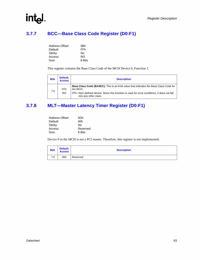
Register Description
3.7.7 BCC—Base Class Code Register (D0:F1)
This register contains the Base Class Code of the MCH Device 0, Function 1.
3.7.8 MLT—Master Latency Timer Register (D0:F1)
Device 0 in the MCH is not a PCI master. Therefore, this register is not implemented.
Address Offset: 0BhDefault: FFhSticky: NoAccess: ROSize: 8 Bits
Bits Default, Access Description
7:0 FFhRO
Base Class Code (BASEC). This is an 8-bit value that indicates the Base Class Code for the MCH. FFh =Non-defined device. Since this function is used for error conditions, it does not fall
into any other class.
Address Offset: 0DhDefault: 00hSticky: NoAccess: Reserved Size: 8 Bits
Bits Default, Access Description
7:0 00h Reserved
Datasheet 63

Register Description
3.7.9 HDR—Header Type (D0:F1)
This register identifies the header layout of the configuration space. It is hardwired to 80h to indicate a multi-function device.
Address Offset: 0EhDefault: 00h or 80hSticky: NoAccess: ROSize: 8 Bits
Bits Default, Access Description
7:0 00h or
80hRO
PCI Header (HDR). This read only field always returns 00h or 80h (value depends on Device Not Present Register) to indicate that the MCH is a multi-function device with standard header layout.
64 Datasheet

Register Description
3.7.10 SVID—Subsystem Vendor Identification Register (D0:F1)
This value is used to identify the vendor of the subsystem.
3.7.11 SID—Subsystem Identification Register (D0:F1)
This value is used to identify a particular subsystem.
Address Offset: 2ChDefault: 0000hSticky: NoAccess: R/WOSize: 16 Bits
Bits Default, Access Description
15:0 0000hR/WO
Subsystem Vendor ID (SUBVID). This field should be programmed during boot-up to indicate the vendor of the system board. After it has been written once, it becomes read only.
Address Offset: 2EhDefault: 0000hSticky: NoAccess: R/WOSize: 16 Bits
Bits Default, Access Description
15:0 0000hR/WO
Subsystem ID (SUBID). This field should be programmed during BIOS initialization. After it has been written once, it becomes read only.
Datasheet 65

Register Description
3.7.12 FERR_GLOBAL—Global Error Register (D0:F1)
This register is used to report various error conditions. An SERR is generated on a 0-to-1 transition of any of these flags (if enabled by the ERRCMD and PCICMD registers). These bits are set regardless of whether or not the SERR is enabled and generated.
This register stores the FIRST global error. Any future errors (NEXT errors) will be set in the NERR_Global Register. No further error bits in this register will be set until the existing error bit is cleared.
Note: To prevent the same error from being logged twice in FERR_GLOBAL and NERR_GLOBAL, a FERR_GLOBAL bit being set blocks the respective bit in the NERR_GLOBAL Register from being set. In addition, bits [18:16] are grouped such that if any of these bits are set in the FERR_GLOBAL Register, none of the bits [18:16] can be set in the NERR_GLOBAL Register. For example, if HI_A causes its respective FERR_GLOBAL bit to be set, any subsequent DDR, FSB, or HI_A error will not be logged in the NERR_GLOBAL Register. Each of these three bits are part of Device 0 status and having any one of them set in FERR_GLOBAL represents a "Device 0 First Error" occurred. This implementation blocks logging in NERR_GLOBAL of any subsequent "Device 0" errors, and allows only logging of subsequent errors that are from other devices.
Note: Software must write a 1 to clear bits that are set.
Address Offset: 40–43hDefault: 0000_0000hSticky: YesAccess: R/WCSize: 32 Bits
Bits Default, Access Description
31:19 0000h Reserved
180b
R/WC
DRAM Interface Error Detected. 0 = No DRAM interface error.1 = MCH detected an error on the DRAM interface.
170b
R/WC
HI_A Error Detected. 0 = No HI_A interface error.1 = MCH detected an error on the HI_A.
16 0b
R/WC
System Bus Error Detected. 0 = No system bus interface error.1 = MCH detected an error on the System Bus.
15:5 000h Reserved
40b
R/WC
HI_D Error Detected. 0 = No HI_D interface error. 1 = MCH detected an error on HI_D.
30b
R/WC
HI_C Error Detected. 0 = No HI_C interface error. 1 = MCH detected an error on HI_C.
20b
R/WC
HI_B Error Detected. 0 = No HI_B interface error. 1 = MCH detected an error on HI_B.
1:0 00b Reserved
66 Datasheet

Register Description
3.7.13 NERR_GLOBAL—Global Error Register (D0:F1)
The FIRST global error will be stored in FERR_GLOBAL. This register stores all future global errors. Multiple bits in this register may be set.
Note: To prevent the same error from being logged twice in FERR_GLOBAL and NERR_GLOBAL, a FERR_GLOBAL bit being set blocks the respective bit in the NERR_GLOBAL Register from being set. In addition, bits [18:16] are grouped such that if any of these bits are set in the FERR_GLOBAL Register, none of the bits [18:16] can be set in the NERR_GLOBAL Register. For example, if HI_A causes its respective FERR_GLOBAL bit to be set, any subsequent DDR, FSB, or HI_A error will not be logged in the NERR_GLOBAL Register. Each of these three bits are part of Device 0 status and having any one of them set in FERR_GLOBAL represents a "Device 0 First Error" occurred. This implementation blocks logging in NERR_GLOBAL of any subsequent "Device 0" errors, and allows only logging of subsequent errors that are from other devices.
Note: Software must write a 1 to clear bits that are set.
Address Offset: 44–47hDefault: 0000_0000hSticky: YesAccess: R/WCSize: 32 Bits
Bits Default, Access Description
31:19 0000h Reserved
180b
R/WC
DRAM Interface Error Detected. 0 = No DRAM interface error detected. 1 = The MCH has detected an error on the DRAM interface.
170b
R/WC
HI_A Error Detected. 0 = No HI_A interface error detected. 1 = The MCH has detected an error on the HI_A.
16 0b
R/WC
System Bus Error Detected. 0 = No system bus interface error detected. 1 = The MCH has detected an error on the System Bus.
15:5 000h Reserved
40b
R/WC
HI_D Error Detected. 0 = No HI_D interface error detected.1 = The MCH has detected an error on HI_D.
30b
R/WC
HI_C Error Detected. 0 = No HI_C interface error detected. 1 = The MCH has detected an error on HI_C.
20b
R/WC
HI_B Error Detected. 0 = No HI_B interface error detected.1 = The MCH has detected an error on HI_B.
1:0 00b Reserved
Datasheet 67

Register Description
3.7.14 HIA_FERR—Hub Interface_A First Error Register (D0:F1)
This register stores the first error related to the HI_A. Only 1 error bit will be set in this register. Any future errors (NEXT errors) will be set the HIA_NERR Register. No further error bits in this register will be set until the existing error bit is cleared.
Note: Software must write a 1 to clear bits that are set.
Address Offset: 50hDefault: 00hSticky: YesAccess: R/WCSize: 8 Bits
Bits Default, Access Description
7 0b Reserved
60b
R/WC
HI_A Target Abort. 0 = No Target Abort on MCH originated HI_A cycle detected.1 = MCH detected that an MCH originated HI_A cycle was terminated with a Target
Abort.
5 0b Reserved
40b
R/WC
HI_A Data Parity Error Detected. 0 = No data parity error detected.1 = MCH detected a parity error on a HI_A data transfer.
3:1 000b Reserved
00b
R/WC
HI_A Address/Command Error Detected. 0 = No address or command parity error detected.1 = MCH detected a parity error on a HI_A address or command.
68 Datasheet

Register Description
3.7.15 HIA_NERR—Hub Interface_A Next Error Register (D0:F1)
The first HI_A error will be stored in the HIA_FERR Register. This register stores all future HI_A errors. Multiple bits in this register may be set.
Note: Software must write a 1 to clear bits that are set.
Address Offset: 52hDefault: 00hSticky: YesAccess: R/WCSize: 8 Bits
Bits Default, Access Description
7 0b Reserved
60b
R/WC
HI_A Target Abort. 0 = No Target Abort on MCH originated HI_A cycle terminated. 1 = MCH originated HI_A cycle was terminated with a Target Abort.
5 0b Reserved
40b
R/WC
HI_A Data Parity Error Detected. 0 = No data parity error detected.1 = Parity error on a HI_A data transfer.
3:1 000b Reserved
00b
R/WC
HI_A Data Address/Command Error Detected. 0 = No address or command parity error detected.1 = Parity error on a HI_A address or command.
Datasheet 69

Register Description
3.7.16 SCICMD_HIA—SCI Command Register (D0:F1)
This register determines whether SCI will be generated when the associated flag is set in the HIA_FERR or HIA_NERR Register. When an error flag is set in the HIA_FERR or HIA_NERR Register, it can generate an SERR, SMI, or SCI when enabled in the SERRCMD, SMICMD, or SCICMD Registers, respectively. Only one message type can be enabled.
Address Offset: 58hDefault: 00hSticky: NoAccess: R/WSize: 8 Bits
Bits Default, Access Description
7 0b Reserved
60b
R/W
SCI on HI_A Target Abort Enable. 0 = No SCI generation 1 = Generate SCI if bit 6 is set in HIA_FERR or HIA_NERR
5 0b Reserved
40b
R/W
SCI on HI_A Data Parity Error Detected Enable. 0 = No SCI generation 1 = Generate SCI if bit 4 is set in HIA_FERR or HIA_NERR
3:1 000b Reserved
00b
R/W
SCI on HI_A Data Address/Comment Error Detected Enable. 0 = No SCI generation 1 = Generate SCI if bit 0 is set in HIA_FERR or HIA_NERR
70 Datasheet

Register Description
3.7.17 SMICMD_HIA—SMI Command Register (D0:F1)
This register determine whether SMI will be generated when the associated flag is set in either the HIA_FERR or HIA_NERR Register. When an error flag is set in the HIA_FERR or HIA_NERR Register, it can generate an SERR, SMI, or SCI when enabled in the SERRCMD, SMICMD, or SCICMD Registers, respectively. Only one message type can be enabled.
Address Offset: 5AhDefault: 00hSticky: NoAccess: R/WSize: 8 Bits
Bits Default, Access Description
7 0b Reserved
60b
R/W
SMI on HI_A Target Abort Enable. 0 = No SMI generation 1 = Generate SMI if bit 6 is set in HIA_FERR or HIA_NERR
5 0b Reserved
40b
R/W
SMI on HI_A Data Parity Error Detected Enable. 0 = No SMI generation 1 = Generate SMI if bit 4 is set in HIA_FERR or HIA_NERR
3:1 000b Reserved
00b
R/W
SMI on HI_A Data Address/Comment Error Detected Enable. 0 = No SMI generation 1 = Generate SMI if bit 0 is set in HIA_FERR or HIA_NERR
Datasheet 71

Register Description
3.7.18 SERRCMD_HIA—SERR Command Register (D0:F1)
This register determine whether SERR will be generated when the associated flag is set in either the HIA_FERR or HIA_NERR Register. When an error flag is set in the HIA_FERR or HIA_NERR Register, it can generate an SERR, SMI, or SCI when enabled in the SERRCMD, SMICMD, or SCICMD Registers, respectively. Only one message type can be enabled.
Address Offset: 5ChDefault: 00hSticky: NoAccess: R/WSize: 8 Bits
Bits Default, Access Description
7 0b Reserved
60b
R/W
SERR on HI_A Target Abort Enable.0 = No SERR generation 1 = Generate SERR if bit 6 is set in HIA_FERR or HIA_NERR
5 0b Reserved
40b
R/W
SERR on HI_A Data Parity Error Detected Enable. 0 = No SERR generation 1 = Generate SERR if bit 4 is set in HIA_FERR or HIA_NERR
3:1 000b Reserved
00b
R/W
SEER on HI_A Data Address/Comment Error Detected Enable. 0 = No SERR generation 1 = Generate SERR if bit 0 is set in HIA_FERR or HIA_NERR
72 Datasheet

Register Description
3.7.19 SYSBUS_FERR—System Bus First Error Register (D0:F1)
This register stores the FIRST error related to the system bus interface. Any future errors (NEXT errors) will be set in the SYSBUS_NERR Register. No further error bits in this register will be set until the existing error bit is cleared.
Note: Software must write a 1 to clear bits that are set.
Address Offset: 60hDefault: 00hSticky: YesAccess: R/WCSize: 8 Bits
Bits Default, Access Description
70b
R/WC
System Bus BINIT# Detected. 0 = No system bus BINT# detected. 1 = This bit is set on an electrical high-to-low transition (0-to-1) of BINIT#.
60b
R/WC
System Bus XERR# Detected. 0 = No system bus XERR# detected.1 = This bit is set on an electrical high-to-low transition (0 to 1) of XERR# on the system
bus.
50b
R/WC
Non-DRAM Lock Error (NDLOCK). 0 = No DRAM lock error detected.1 = MCH detected a lock operation to memory space that did not map into DRAM.
40b
R/WC
System Bus Address Above TOM (SBATOM). 0 = No system bus address above TOM detected.1 = MCH detected an address above DRB7, which is the Top of Memory and above 4 GB.
30b
R/WC
System Bus Data Parity Error (SBDPAR). 0 = No system bus data parity error detected.1 = The MCH has detected a data parity error on the system bus.
20b
R/WC
System Bus Address Strobe Glitch Detected (SBAGL). 0 = No system bus address strobe glitch detected.1 = The MCH has detected a glitch on one of the system bus address strobes.
10b
R/WC
System Bus Data Strobe Glitch Detected (SBDGL). 0 = No system bus data strobe glitch detected.1 = The MCH has detected a glitch on one of the system bus data strobes.
00b
R/WC
System Bus Request/Address Parity Error (SBRPAR). 0 = No system bus request/address parity error detected.1 = MCH detected a parity error on either the address or request signals of the system
bus.
Datasheet 73

Register Description
3.7.20 SYSBUS_NERR—System Bus Next Error Register (D0:F1)
The FIRST system bus error will be stored in the SYSBUS_FERR Register. This register stores all future system bus errors. Multiple bits in this register may be set.
Note: Software must write a 1 to clear bits that are set.
Address Offset: 62hDefault: 00hSticky: YesAccess: R/WCSize: 8 Bits
Bits Default, Access Description
70b
R/WC
System Bus BINIT# Detected. 0 = No system bus BINIT# detected. 1 = This bit is set on an electrical high-to-low transition (0 to 1) of BINIT#.
60b
R/WC
System Bus XERR# Detected. 0 = No system bus XERR# detected. 1 = This bit is set on an electrical high-to-low transition (0 to 1) of XERR# on the system
bus.
50b
R/WC
Non-DRAM Lock Error (NDLOCK). 0 = No non-DRAM lock error detected.1 = The MCH has detected a lock operation to memory space that did not map into
DRAM.
40b
R/WC
System Bus Address Above TOM (SBATOM). 0 = No system bus address above TOM detected.1 = MCH detected an address above DRB7, which is the Top of Memory and above 4 GB.
30b
R/WC
System Bus Data Parity Error (SBDPAR). 0 = No system bus data parity error detected.1 = MCH detected a data parity error on the system bus.
20b
R/WC
System Bus Address Strobe Glitch Detected (SBAGL). 0 = No system bus address strobe glitch detected.1 = MCH detected a glitch on one of the system bus address strobes.
10b
R/WC
System Bus Data Strobe Glitch Detected (SBDGL). 0 = No System Bus Data Strobe Glitch detected.1 = MCH detected a glitch on one of the system bus data strobes.
00b
R/WC
System Bus Request/Address Parity Error (SBRPAR). 0 = No system bus request/address parity error detected.1 = MCH detected a parity error on either the address or request signals of the system
bus.
74 Datasheet

Register Description
3.7.21 SCICMD_SYSBUS—SCI Command Register (D0:F1)
This register determine whether SCI will be generated when the associated flag is set in either the SYSBUS_FERR or SYSBUS_NERR Register. When an error flag is set in the SYSBUS_FERR or SYSBUS_NERR Register, it can generate an SERR, SMI, or SCI when enabled in the SERRCMD, SMICMD, or SCICMD Registers, respectively. Only one message type can be enabled.
Address Offset: 68hDefault: 00hSticky: NoAccess: R/WSize: 8 Bits
Bits Default, Access Description
70b
R/W
SCI on System Bus BINIT# Detected Enable. 0 = No SCI generation 1 = Generate SCI if bit 7 is set in SYSBUS_FERR or SYSBUS_NERR
60b
R/W
SCI on System Bus xERR# Detected Enable. 0 = No SCI generation 1 = Generate SCI if bit 6 is set in SYSBUS_FERR or SYSBUS_NERR
50b
R/W
SCI on Non-DRAM Lock Error Enable. 0 = No SCI generation 1 = Generate SCI if bit 5 is set in SYSBUS_FERR or SYSBUS_NERR
40b
R/W
SCI on System Bus Address Above TOM Enable. 0 = No SCI generation 1 = Generate SCI if bit 4 is set in SYSBUS_FERR or SYSBUS_NERR
30b
R/W
SCI on System Bus Data Parity Error Enable. 0 = No SCI generation 1 = Generate SCI if bit 3 is set in SYSBUS_FERR or SYSBUS_NERR
20b
R/W
SCI on System Bus Address Strobe Glitch Detected Enable. 0 = No SCI generation 1 = Generate SCI if bit 2 is set in SYSBUS_FERR or SYSBUS_NERR
10b
R/W
SCI on System Bus Data Strobe Glitch Detected Enable. 0 = No SCI generation 1 = Generate SCI if bit 1 is set in SYSBUS_FERR or SYSBUS_NERR
00b
R/W
SCI on System Bus Request/Address Parity Error Enable. 0 = No SCI generation 1 = Generate SCI if bit 0 is set in SYSBUS_FERR or SYSBUS_NERR
Datasheet 75

Register Description
3.7.22 SMICMD_SYSBUS—SMI Command Register (D0:F1)
This register determines whether SMI will be generated when the associated flag is set in either the SYSBUS_FERR or SYSBUS_NERR Register. When an error flag is set in the SYSBUS_FERR or SYSBUS_NERR Register, it can generate an SERR, SMI, or SCI when enabled in the SERRCMD, SMICMD, or SCICMD Registers, respectively. Only one message type can be enabled.
Address Offset: 6AhDefault: 00hSticky: NoAccess: R/WSize: 8 Bits
Bits Default, Access Description
70b
R/W
SMI on System Bus BINIT# Detected Enable.0 = No SMI generation 1 = Generate SMI if bit 7 is set in SYSBUS_FERR or SYSBUS_NERR
60b
R/W
SMI on System Bus xERR# Detected Enable. 0 = No SMI generation 1 = Generate SMI if bit 6 is set in SYSBUS_FERR or SYSBUS_NERR
50b
R/W
SMI on Non-DRAM Lock Error Enable. 0 = No SMI generation 1 = Generate SMI if bit 5 is set in SYSBUS_FERR or SYSBUS_NERR
40b
R/W
SMI on System Bus Address Above TOM Enable. 0 = No SMI generation 1 = Generate SMI if bit 4 is set in SYSBUS_FERR or SYSBUS_NERR
30b
R/W
SMI on System Bus Data Parity Error Enable. 0 = No SMI generation 1 = Generate SMI if bit 3 is set in SYSBUS_FERR or SYSBUS_NERR
20b
R/W
SMI on System Bus Address Strobe Glitch Detected Enable. 0 = No SMI generation 1 = Generate SMI if bit 2 is set in SYSBUS_FERR or SYSBUS_NERR
10b
R/W
SMI on System Bus Data Strobe Glitch Detected Enable. 0 = No SMI generation 1 = Generate SMI if bit 1 is set in SYSBUS_FERR or SYSBUS_NERR
00b
R/W
SMI on System Bus Request/Address Parity Error Enable. 0 = No SMI generation 1 = Generate SMI if bit 0 is set in SYSBUS_FERR or SYSBUS_NERR
76 Datasheet
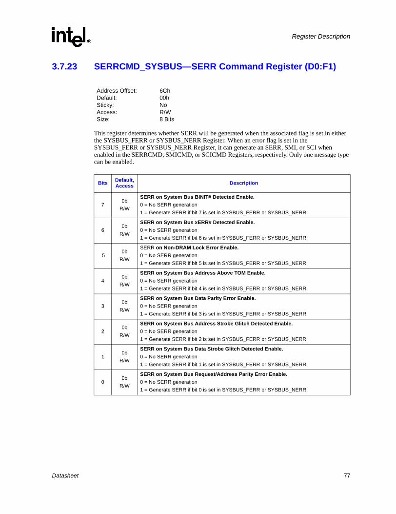
Register Description
3.7.23 SERRCMD_SYSBUS—SERR Command Register (D0:F1)
This register determines whether SERR will be generated when the associated flag is set in either the SYSBUS_FERR or SYSBUS_NERR Register. When an error flag is set in the SYSBUS_FERR or SYSBUS_NERR Register, it can generate an SERR, SMI, or SCI when enabled in the SERRCMD, SMICMD, or SCICMD Registers, respectively. Only one message type can be enabled.
Address Offset: 6ChDefault: 00hSticky: NoAccess: R/WSize: 8 Bits
Bits Default, Access Description
70b
R/W
SERR on System Bus BINIT# Detected Enable.0 = No SERR generation 1 = Generate SERR if bit 7 is set in SYSBUS_FERR or SYSBUS_NERR
60b
R/W
SERR on System Bus xERR# Detected Enable. 0 = No SERR generation 1 = Generate SERR if bit 6 is set in SYSBUS_FERR or SYSBUS_NERR
50b
R/W
SERR on Non-DRAM Lock Error Enable. 0 = No SERR generation 1 = Generate SERR if bit 5 is set in SYSBUS_FERR or SYSBUS_NERR
40b
R/W
SERR on System Bus Address Above TOM Enable. 0 = No SERR generation 1 = Generate SERR if bit 4 is set in SYSBUS_FERR or SYSBUS_NERR
30b
R/W
SERR on System Bus Data Parity Error Enable.0 = No SERR generation1 = Generate SERR if bit 3 is set in SYSBUS_FERR or SYSBUS_NERR
20b
R/W
SERR on System Bus Address Strobe Glitch Detected Enable.0 = No SERR generation 1 = Generate SERR if bit 2 is set in SYSBUS_FERR or SYSBUS_NERR
10b
R/W
SERR on System Bus Data Strobe Glitch Detected Enable. 0 = No SERR generation 1 = Generate SERR if bit 1 is set in SYSBUS_FERR or SYSBUS_NERR
00b
R/W
SERR on System Bus Request/Address Parity Error Enable. 0 = No SERR generation1 = Generate SERR if bit 0 is set in SYSBUS_FERR or SYSBUS_NERR
Datasheet 77

Register Description
3.7.24 DRAM_FERR—DRAM First Error Register (D0:F1)
This register stores the FIRST ECC error on the DRAM interface. Only 1 error bit will be set in this register. Any future errors (NEXT errors) will be set in the DRAM_NERR Register. No further error bits in this register will be set until the existing error bit is cleared.
Note: Software must write a 1 to clear bits that are set.
3.7.25 DRAM_NERR—DRAM Next Error Register (D0:F1)
The FIRST memory ECC error will be stored in the DRAM_FERR Register. This register stores all future memory ECC errors. Multiple bits in this register may be set.
Note: Software must write a 1 to clear bits that are set.
Address Offset: 80hDefault: 00hSticky: YesAccess: R/WCSize: 8 Bits
Bits Default, Access Description
7:2 00h Reserved
10b
R/WC
Uncorrectable Memory Error Detected. 0 = No uncorrectable memory error detected.1 = MCH detected an ECC error on the memory interface that is not correctable.
00b
R/WC
Correctable Memory Error Detected. 0 = No correctable memory error detected.1 = MCH detected and corrected an ECC error on the memory interface.
Address Offset: 82hDefault: 00hSticky: YesAccess: R/WCSize: 8 Bits
Bits Default, Access Description
7:2 00h Reserved
10b
R/WC
Uncorrectable Memory Error Detected. 0 = No uncorrectable memory error detected.1 = The MCH has detected an ECC error on the memory interface that is not correctable.
00b
R/WC
Correctable Memory Error Detected. 0 = No correctable memory error detected.1 = The MCH has detected and corrected an ECC error on the memory interface.
78 Datasheet

Register Description
3.7.26 SCICMD_DRAM—SCI Command Register (D0:F1)
This register determines whether SCI will be generated when the associated flag is set in either the DRAM_FERR or DRAM_NERR Register. When an error flag is set in the DRAM_FERR or DRAM_NERR Register, it can generate an SERR, SMI, or SCI when enabled in the SERRCMD, SMICMD, or SCICMD Registers, respectively. Only one message type can be enabled.
3.7.27 SMICMD_DRAM—SMI Command Register (D0:F1)
This register determines whether SMI will be generated when the associated flag is set in the DRAM_FERR or DRAM_NERR Register. When an error flag is set in the DRAM_FERR or DRAM_NERR Register, it can generate an SERR, SMI, or SCI when enabled in the SERRCMD, SMICMD, or SCICMD Registers, respectively. Only one message type can be enabled.
Address Offset: 88hDefault: 00hSticky: NoAccess: R/WSize: 8 Bits
Bits Default, Access Description
7:2 000000b Reserved
10b
R/W
SCI on Multiple-Bit DRAM ECC Error (DMERR). 0 = Disable.1 = Enable. The MCH generates an SCI when it detects a multiple-bit error reported by
the DRAM controller.
00b
R/W
SCI on Single-Bit DRAM ECC Error (DSERR). 0 = Disable.1 = Enable. The MCH generates an SCI when the DRAM controller detects a single-bit
error.
Address Offset: 8AhDefault: 00hSticky: NoAccess: R/WSize: 8 Bits
Bits Default, Access Description
7:2 000000b Reserved
10b
R/W
SMI on Multiple-Bit DRAM ECC Error (DMERR). 0 = Disable.1 = Enable. The MCH generates an SMI when it detects a multiple-bit error reported by
the DRAM controller.
00b
R/W
SMI on Single-Bit DRAM ECC Error (DSERR). 0 = Disable.1 = Enable. The MCH generates an SMI when the DRAM controller detects a single-bit
error.
Datasheet 79

Register Description
3.7.28 SERRCMD_DRAM—SERR Command Register (D0:F1)
This register determines whether SERR will be generated when the associated flag is set in either the DRAM_FERR or DRAM_NERR Register. When an error flag is set in the DRAM_FERR or DRAM_NERR Register, it can generate an SERR, SMI, or SCI when enabled in the SERRCMD, SMICMD, or SCICMD Registers, respectively. Only one message type can be enabled.
3.7.29 DRAM_CELOG_ADD—DRAM First Correctable Memory Error Address Register (D0:F1)
This register contains the address of the first correctable memory error. This register is locked when bits in either the DRAM_FERR or DRAM_NERR Registers are set. If the bits in both registers are set to 0, the DRAM_CELOG_ADD can be updated; however, if a bit in either register is set to 1, then DRAM_CELOG_ADD will retain its value for logging purposes. This register is only valid if a bit in either the DRAM_FERR or DRAM_NERR Register is set.
Address Offset: 8ChDefault: 00hSticky: NoAccess: R/WSize: 8 Bits
Bits Default, Access Description
7:2 000000b Reserved
10b
R/W
SERR on Multiple-Bit DRAM ECC Error (DMERR). 0 = Disable.1 = Enable. The MCH generates an SERR when it detects a multiple-bit error reported by
the DRAM controller.
00b
R/W
SERR on Single-Bit DRAM ECC Error (DSERR). 0 = Disable.1 = Enable. The MCH generates an SERR when the DRAM controller detects a single-bit
error.
Address Offset: A0–A3hDefault: 0000_0000hSticky: YesAccess: ROSize: 32 Bits
Bits Default, Access Description
31:28 0h Reserved
27:6000000h
ROCE Address. This field contains address bits 33:12 of the first correctable memory error. The address bits are a physical address.
5:0 00h Reserved
80 Datasheet

Register Description
3.7.30 DRAM_UELOG_ADD—DRAM First Uncorrectable Memory Error Address Register (D0:F1)
This register contains the address of the first uncorrectable memory error. When a bit in either the DRAM_FERR or DRAM_NERR Register is set, this register is locked. This register is only valid if a bit in either the DRAM_FERR or DRAM_NERR Register is set.
3.7.31 DRAM_CELOG_SYNDROME—DRAM First Correctable Memory Error Register (D0:F1)
This register contains the syndrome of the first correctable memory error. This register is locked when a bit in either the DRAM_FERR or DRAM_NERR Register is set. If the bits in both registers are set to 0, the DRAM_CELOG_SYNDROME can be updated; however, if a bit in either register is set to 1, then DRAM_CELOG_SYNDROME will retain its value for logging purposes. This register is only valid if a bit in either the DRAM_FERR or DRAM_NERR Register is set.
Address Offset: B0–B3hDefault: 0000_0000hSticky: YesAccess: ROSize: 32 Bits
Bits Default, Access Description
31:28 0h Reserved
27:6000000h
ROUE Address. This field contains address bits 33:12 of the first uncorrectable memory error. The address bits are a physical address.
5:0 00h Reserved
Address Offset: D0–D1hDefault: 0000hSticky: YesAccess: ROSize: 16 Bits
Bits Default, Access Description
15:00000h
ROECC Syndrome for Correctable Errors.
Datasheet 81

Register Description
3.8 HI_B Virtual PCI-to-PCI Bridge Registers (Device 2, Function 0)This section provides the register descriptions for the HI_B virtual PCI-to-PCI bridge (Device 2, Function 0). Table 3-5 provides the register address map for this device, function.
Warning: Address locations that are not listed the table are considered reserved register locations. Writes to “Reserved” registers may cause system failure. Reads to “Reserved” registers may return a non-zero value.
Table 3-5. HI_B Virtual PCI-to-PCI Bridge Register Map (HI_A—D2:F0)
Offset Mnemonic Register Name Default Type
00–01h VID2 Vendor ID 8086h RO
02–03h DID2 Device ID 2543h RO
04–05h PCICMD2 PCI Command 0000h RO, R/W
06–07h PCISTS2 PCI Status 00A0h RO, R/WC
08h RID2 Revision ID 02h RO
0Ah SUBC2 Sub Class Code 04h RO
0Bh BCC2 Base Class Code 06h RO
0Dh MLT2 Master Latency Timer 00h R/W
0Eh HDR2 Header Type 01h or 81h RO
18h PBUSN2 Primary Bus Number 00h RO
19h BUSN2 Secondary Bus Number 00h R/W
1Ah SUBUSN2 Subordinate Bus Number 00h R/W
1Bh SMLT2 Secondary Bus Master Latency Timer 00h Reserved
1Ch IOBASE2 I/O Base Address F0h R/W
1Dh IOLIMIT2 I/O Limit Address 00h R/W
1E–1Fh SEC_STS2 Secondary Status 0160 RO, R/WC
20–21h MBASE2 Memory Base Address FFF0h R/W
22–23h MLIMIT2 Memory Limit Address 0000h R/W
24–25h PMBASE2 Prefetchable Memory Base Address FFF0h RO, R/W
26–27h PMLIMIT2 Prefetchable Memory Limit Address 0000h RO, R/W
3Eh BCTRL2 Bridge Control 00h RO, R/W
82 Datasheet

Register Description
3.8.1 VID2—Vendor Identification Register (D2:F0)
The VID Register contains the vendor identification number. This 16-bit register combined with the Device Identification Register uniquely identify any PCI device.
3.8.2 DID2—Device Identification Register (D2:F0)
This 16-bit register combined with the Vendor Identification register uniquely identifies any PCI device.
Address Offset: 00–01hDefault: 8086hSticky: NoAccess: RO Size: 16 Bits
Bits Default, Access Description
15:0 8086h
ROVendor Identification Device 2 (VID2). This register field contains the PCI standard identification for Intel (VID=8086h).
Address Offset: 02–03hDefault: 2543hSticky: NoAccess: RO Size: 16 Bits
Bits Default, Access Description
15:0 2543h
RODevice Identification Number (DID). This is a 16-bit value assigned to the MCH device 2.
Datasheet 83

Register Description
3.8.3 PCICMD2—PCI Command Register (D2:F0)
Since MCH Device 0 does not physically reside on a physical PCI bus, portions of this register are not implemented.
Address Offset: 04–05hDefault: 0000hSticky: NoAccess: RO R/W Size: 16 Bits
Bits Default, Access Description
15:10 00h Reserved
9 0bRO
Fast Back-to-Back Enable (FB2B). Not Applicable; hardwired to 0.
8 0b
R/W
SERR Message Enable (SERRE). This bit is a global enable bit for Device 2 SERR messaging. The MCH does not have an SERR# signal. The MCH communicates the SERR# condition by sending an SERR message to the ICH3-S. 0 = SERR message is not generated by the MCH for Device 2.1 = The MCH is enabled to generate SERR messages over HI_A for specific Device 2
error conditions.
7 0bRO
Address/Data Stepping (ADSTEP). Not applicable; this bit is hardwired to 0.
6 0bRO
Parity Error Enable (PERRE). Hardwired to 0. Parity checking is not supported on the primary side of this device.
5 0b Reserved
4 0bRO
Memory Write and Invalidate Enable (MWIE). Not applicable; hardwired to 0.
3 0bRO
Special Cycle Enable (SCE). Not applicable; hardwired to 0.
2 0b
R/WBus Master Enable (BME). This bit is not functional. It is a R/W bit for compatibility with compliance testing software.
1 0b
R/W
Memory Access Enable (MAE). 0 = Disable. All of device 2’s memory space is disabled.1 = Enable. This bit must be set to 1 to enable the Memory and Prefetchable memory
address ranges defined in the MBASE2, MLIMIT2, PMBASE2, and PMLIMIT2 Registers.
0 0b
R/W
IO Access Enable (IOAE). 0 = Disable. All of device 2’s I/O space is disabled.1 = Enable. This bit must be set to 1 to enable the I/O address range defined in the
IOBASE2 and IOLIMIT2 Registers.
84 Datasheet
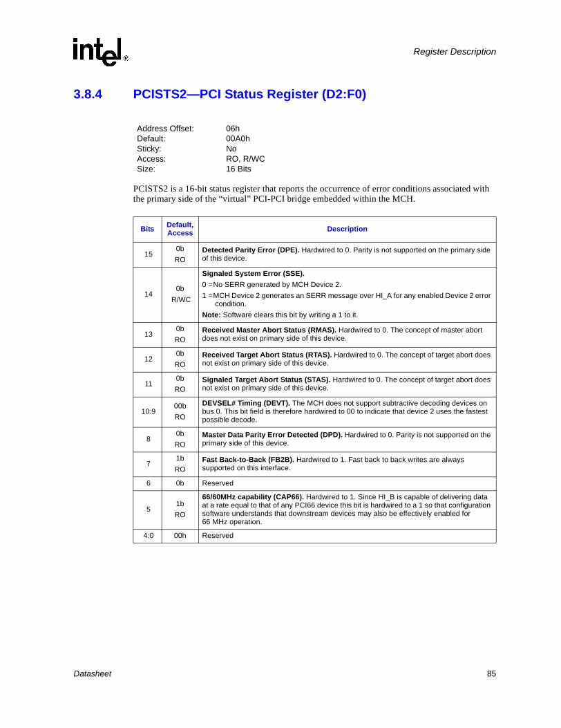
Register Description
3.8.4 PCISTS2—PCI Status Register (D2:F0)
PCISTS2 is a 16-bit status register that reports the occurrence of error conditions associated with the primary side of the “virtual” PCI-PCI bridge embedded within the MCH.
Address Offset: 06hDefault: 00A0hSticky: NoAccess: RO, R/WC Size: 16 Bits
Bits Default, Access Description
15 0bRO
Detected Parity Error (DPE). Hardwired to 0. Parity is not supported on the primary side of this device.
14 0b
R/WC
Signaled System Error (SSE). 0 =No SERR generated by MCH Device 2.1 =MCH Device 2 generates an SERR message over HI_A for any enabled Device 2 error
condition. Note: Software clears this bit by writing a 1 to it.
13 0bRO
Received Master Abort Status (RMAS). Hardwired to 0. The concept of master abort does not exist on primary side of this device.
12 0bRO
Received Target Abort Status (RTAS). Hardwired to 0. The concept of target abort does not exist on primary side of this device.
11 0bRO
Signaled Target Abort Status (STAS). Hardwired to 0. The concept of target abort does not exist on primary side of this device.
10:9 00bRO
DEVSEL# Timing (DEVT). The MCH does not support subtractive decoding devices on bus 0. This bit field is therefore hardwired to 00 to indicate that device 2 uses the fastest possible decode.
8 0bRO
Master Data Parity Error Detected (DPD). Hardwired to 0. Parity is not supported on the primary side of this device.
7 1bRO
Fast Back-to-Back (FB2B). Hardwired to 1. Fast back to back writes are always supported on this interface.
6 0b Reserved
5 1bRO
66/60MHz capability (CAP66). Hardwired to 1. Since HI_B is capable of delivering data at a rate equal to that of any PCI66 device this bit is hardwired to a 1 so that configuration software understands that downstream devices may also be effectively enabled for 66 MHz operation.
4:0 00h Reserved
Datasheet 85
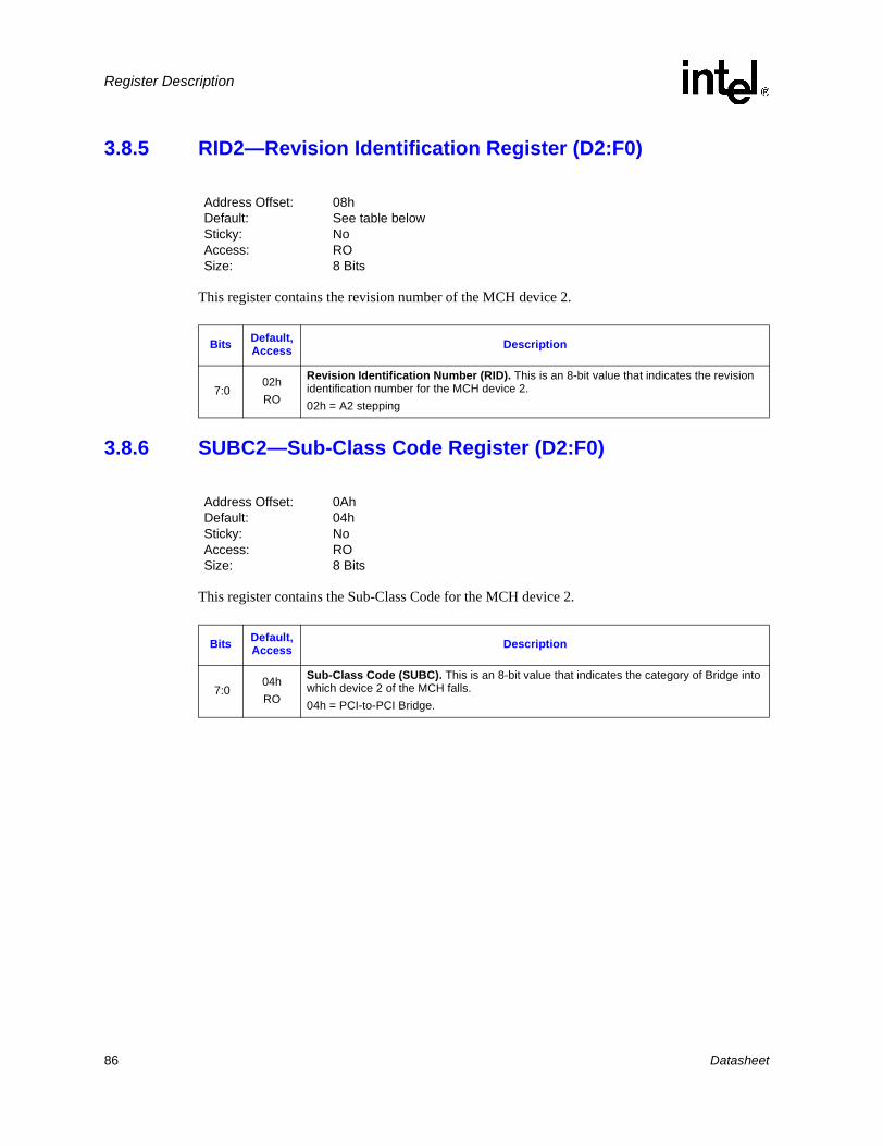
Register Description
3.8.5 RID2—Revision Identification Register (D2:F0)
This register contains the revision number of the MCH device 2.
3.8.6 SUBC2—Sub-Class Code Register (D2:F0)
This register contains the Sub-Class Code for the MCH device 2.
Address Offset: 08hDefault: See table belowSticky: NoAccess: RO Size: 8 Bits
Bits Default, Access Description
7:0 02hRO
Revision Identification Number (RID). This is an 8-bit value that indicates the revision identification number for the MCH device 2. 02h = A2 stepping
Address Offset: 0AhDefault: 04hSticky: NoAccess: RO Size: 8 Bits
Bits Default, Access Description
7:0 04hRO
Sub-Class Code (SUBC). This is an 8-bit value that indicates the category of Bridge into which device 2 of the MCH falls. 04h = PCI-to-PCI Bridge.
86 Datasheet

Register Description
3.8.7 BCC2—Base Class Code Register (D2:F0)
This register contains the Base Class Code of the MCH device 2.
3.8.8 MLT2—Master Latency Timer Register (D2:F0)
This functionality is not applicable. It is described here since these bits should be implemented as read/write to ensue proper execution of standard PCI-to-PCI bridge configuration software.
Address Offset: 0BhDefault: 06hSticky: NoAccess: RO Size 8 Bits
Bits Default, Access Description
7:0 06hRO
Base Class Code (BASEC). This is an 8-bit value that indicates the Base Class Code for the MCH device 2. 06h = Bridge device
Address Offset: 0DhDefault: 00hSticky: NoAccess: R/W Size: 8 Bits
Bits Default, Access Description
7:3 00h
R/WScratchpad MLT (NA7.3). These bits return the value with which they are written; however, they have no internal function and are implemented as a scratchpad.
2:0 000b Reserved
Datasheet 87

Register Description
3.8.9 HDR2—Header Type Register (D2:F0)
This register identifies the header layout of the configuration space.
3.8.10 PBUSN2—Primary Bus Number Register (D2:F0)
This register identifies that “virtual” PCI-PCI bridge is connected to bus 0.
Address Offset: 0EhDefault: 01h or 81hSticky: NoAccess: RO Size: 8 Bits
Bits Default, Access Description
7:0 01h or
81hRO
Header Type Register (HDR). When Function 1 is enabled, this read only field returns 81h to indicate that MCH device 2 is a multi-function device with bridge header layout. When Function 1 is disabled, 01h is returned to indicate that MCH device 2 is a single-function device with bridge layout. Writes to this location have no effect.
Address Offset: 18hDefault: 00hSticky: NoAccess: RO Size: 8 Bits
Bits Default, Access Description
7:0 00hRO
Primary Bus Number (BUSN). Configuration software typically programs this field with the number of the bus on the primary side of the bridge. Since device 2 is an internal device and its primary bus is always 0, these bits are read only and are hardwired to 0.
88 Datasheet

Register Description
3.8.11 BUSN2—Secondary Bus Number Register (D2:F0)
This register identifies the bus number assigned to the second bus side of the “virtual” PCI-PCI bridge (the HI_B connection). This number is programmed by the PCI configuration software to allow mapping of configuration cycles to a second bridge device connected to HI_B.
3.8.12 SUBUSN2—Subordinate Bus Number Register (D2:F0)
This register identifies the subordinate bus (if any) that resides at the level below the secondary HI. This number is programmed by the PCI configuration software to allow mapping of configuration cycles to devices subordinate to the secondary HI.
Address Offset: 19hDefault: 00hSticky: NoAccess: R/W Size: 8 Bits
Bits Default, Access Description
7:0 00hR/W
Secondary Bus Number (BUSN). This field is programmed by configuration software with the lowest bus number of the busses connected to HI_B. Since both bus 0, device 2 and the PCI to PCI bridge on the other end of the HI are considered by configuration software to be PCI bridges, this bus number will always correspond to the bus number assigned to HI_B.
Address Offset: 1AhDefault: 00hSticky: NoAccess: R/W Size: 8 Bits
Bits Default, Access Description
7:0 00hR/W
Subordinate Bus Number (BUSN). This register is programmed by configuration software with the number of the highest subordinate bus that lies behind the device 2 bridge.
Datasheet 89
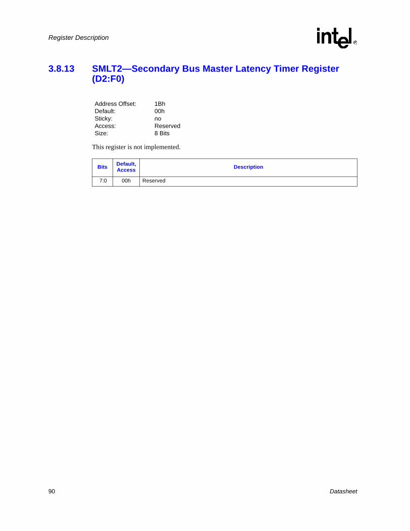
Register Description
3.8.13 SMLT2—Secondary Bus Master Latency Timer Register (D2:F0)
This register is not implemented.
Address Offset: 1BhDefault: 00hSticky: noAccess: ReservedSize: 8 Bits
Bits Default, Access Description
7:0 00h Reserved
90 Datasheet
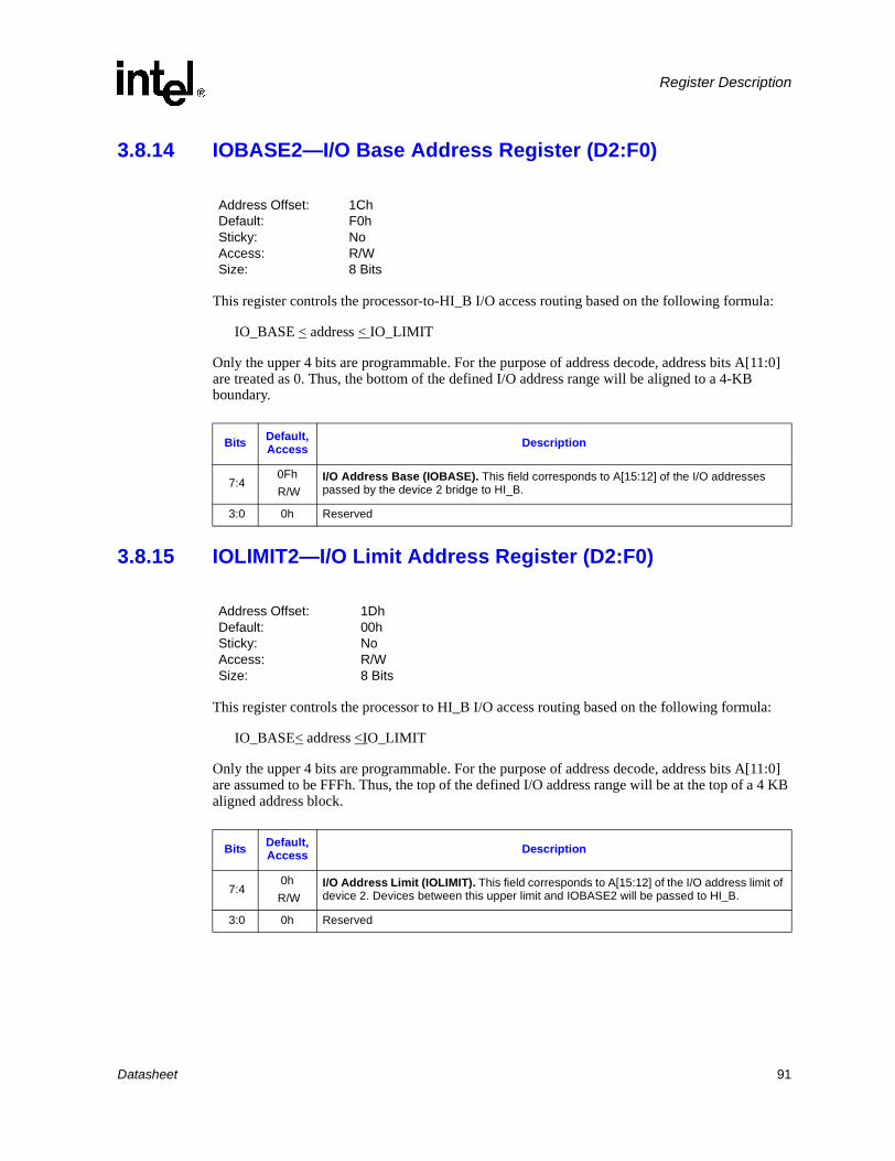
Register Description
3.8.14 IOBASE2—I/O Base Address Register (D2:F0)
This register controls the processor-to-HI_B I/O access routing based on the following formula:
IO_BASE < address < IO_LIMIT
Only the upper 4 bits are programmable. For the purpose of address decode, address bits A[11:0] are treated as 0. Thus, the bottom of the defined I/O address range will be aligned to a 4-KB boundary.
3.8.15 IOLIMIT2—I/O Limit Address Register (D2:F0)
This register controls the processor to HI_B I/O access routing based on the following formula:
IO_BASE< address <IO_LIMIT
Only the upper 4 bits are programmable. For the purpose of address decode, address bits A[11:0] are assumed to be FFFh. Thus, the top of the defined I/O address range will be at the top of a 4 KB aligned address block.
Address Offset: 1ChDefault: F0hSticky: NoAccess: R/W Size: 8 Bits
Bits Default, Access Description
7:4 0Fh R/W
I/O Address Base (IOBASE). This field corresponds to A[15:12] of the I/O addresses passed by the device 2 bridge to HI_B.
3:0 0h Reserved
Address Offset: 1DhDefault: 00hSticky: NoAccess: R/W Size: 8 Bits
Bits Default, Access Description
7:4 0h
R/WI/O Address Limit (IOLIMIT). This field corresponds to A[15:12] of the I/O address limit of device 2. Devices between this upper limit and IOBASE2 will be passed to HI_B.
3:0 0h Reserved
Datasheet 91

Register Description
3.8.16 SEC_STS2—Secondary Status Register (D2:F0)
SSTS2 is a 16-bit status register that reports the occurrence of error conditions associated with secondary side (i.e., HI_B side) of the “virtual” PCI-PCI bridge embedded within the MCH.
Note: Software must write a 1 to clear bits that are set.
Address Offset: 1E–1FhDefault: 0160hSticky: NoAccess: RO, R/WC Size: 16 Bits
Bits Default, Access Description
15 0b
R/WC
Detected Parity Error (2DPE). 0 = No parity error detected. 1 = MCH detected a parity error in the address or data phase of HI_B bus transactions.
14 0b
R/WC
Received System Error (2RSE). 0 = No system error received. 1 = This bit is set to 1 when the MCH receives an SERR message on HI_B.
13 0b
R/WC
Received Master Abort Status (2RMAS). 0 = No Master Abort received. 1 = The MCH received a Master Abort completion packet on HI_B.
12 0b
R/WC
Received Target Abort Status (2RTAS). 0 = No Target Abort received. 1 = The MCH received a Target Abort completion packet on HI_B.
11 0bRO
Signaled Target Abort Status (STAS). Hardwired to 0. The MCH does not generate target aborts on HI_B.
10:9 01bRO
DEVSEL# Timing (DEVT). Hardwired to 01. This concept is not supported on HI_B.
8 0bRO
Master Data Parity Error Detected (DPD). Hardwired to 0. The MCH does not implement PERR messaging on HI_B.
7 1bRO
Fast Back-to-Back (FB2B). Hardwired to 1. This function is not supported on HI_B.
6 0b Reserved
5 1bRO
66/60 MHz capability (CAP66). Hardwired to 1. HI_B is enabled for 66 MHz operation.
4:0 00h Reserved
92 Datasheet

Register Description
3.8.17 MBASE2—Memory Base Address Register (D2:F0)
This register controls the processor to HI_B non-prefetchable memory access routing based on the following formula:
MEMORY_BASE < address < MEMORY_LIMIT
The upper 12 bits of the register are read/write and correspond to the upper 12 address bits A[31:20] of the 32 bit address. The bottom 4 bits of this register are read-only and return 0s when read. This register must be initialized by the configuration software. For the purpose of address decode, address bits A[19:0] are assumed to be 0. The bottom of the defined memory address range will be aligned to a 1-MB boundary.
Address Offset: 20–21hDefault: FFF0hSticky: NoAccess: R/W Size: 16 Bits
Bits Default, Access Description
15:4 FFFhR/W
Memory Address Base (MBASE). This field corresponds to A[31:20] of the lower limit of the memory range that will be passed by the device 2 bridge to HI_B.
3:0 0h Reserved
Datasheet 93

Register Description
3.8.18 MLIMIT2—Memory Limit Address Register (D2:F0)
This register controls the processor to HI_B non-prefetchable memory access routing based on the following formula:
MEMORY_BASE < address < MEMORY_LIMIT
The upper 12 bits of the register are read/write and correspond to the upper 12 address bits A[31:20] of the 32-bit address. The bottom four bits of this register are read-only and return 0s when read. This register must be initialized by the configuration software. For the purpose of address decode, address bits A[19:0] are assumed to be FFFFFh. Thus, the top of the defined memory address range will be at the top of a 1-MB aligned memory block.
Note: The memory range covered by the MBASE and MLIMIT Registers are used to map non-prefetchable HI_B address ranges (typically where control/status memory-mapped I/O data structures of the graphics controller will reside) and PMBASE and PMLIMIT are used to map prefetchable address ranges (typically graphics local memory). This segregation allows application of USWC space attribute to be performed in a true plug-and-play manner to the prefetchable address range for improved HI memory access performance.
Configuration software is responsible for programming all address range registers (prefetchable, non-prefetchable) with the values that provide exclusive address ranges (i.e., prevent overlap with each other and/or with the ranges covered with the main memory). There is no provision in the MCH hardware to enforce prevention of overlap and operations of the system in the case of overlap are not guaranteed.
Address Offset: 22–23hDefault: 0000hSticky: NoAccess: R/W Size: 16 Bits
Bits Default, Access Description
15:4 000hR/W
Memory Address Limit (MILIMIT). This field corresponds to A[31:20] of the memory address that corresponds to the upper limit of the range of memory accesses that will be passed by the device 2 bridge to HI_B
3:0 0h Reserved
94 Datasheet

Register Description
3.8.19 PMBASE2—Prefetchable Memory Base Address Register (D2:F0)
This register controls the processor to HI_B prefetchable memory accesses. See PM64BASE2 for usage. The upper 12 bits of the register are read/write and correspond to the upper 12 address bits A[31:20] of the 36-bit address. For the purpose of address decode, bits A[19:0] are assumed to be 0. Thus, the bottom of the defined memory address range will be aligned to a 1-MB boundary.
3.8.20 PMLIMIT2—Prefetchable Memory Limit Address Register (D2:F0)
This register controls the processor to HI_B prefetchable memory accesses. See PM64BASE2 for usage. The upper 12 bits of the register are read/write and correspond to the upper 12 address bits A[31:20] of the 36-bit address. For the purpose of address decode, bits A[19:0] are assumed to be FFFFh. Thus, the top of the defined memory address range will be at the top of a 1-MB aligned memory block.
Address Offset: 24–25hDefault: FFF0hSticky: NoAccess: RO, R/W Size: 16 Bits
Bits Default, Access Description
15:4 FFFh R/W
Prefetchable Memory Address Base (PMBASE). This field corresponds to A[31:20] of the lower limit of the address range passed by bridge device 2 across HI_B.
3:0 0hRO
64-bit Addressing Support. Hardwired to 0. The MCH does not support Outbound 64-bit addressing.
Address Offset: 26hDefault: 0000hSticky: NoAccess: RO, R/W Size: 16 Bits
Bits Default, Access Description
15:4 000h R/W
Prefetchable Memory Address Limit (PMLIMIT). This field corresponds to A[31:20] of the upper limit of the address range passed by bridge device 2 across HI_B.
3:0 0hRO
64-bit Addressing Support. Hardwired to 0. The MCH does not support Outbound 64-bit addressing.
Datasheet 95
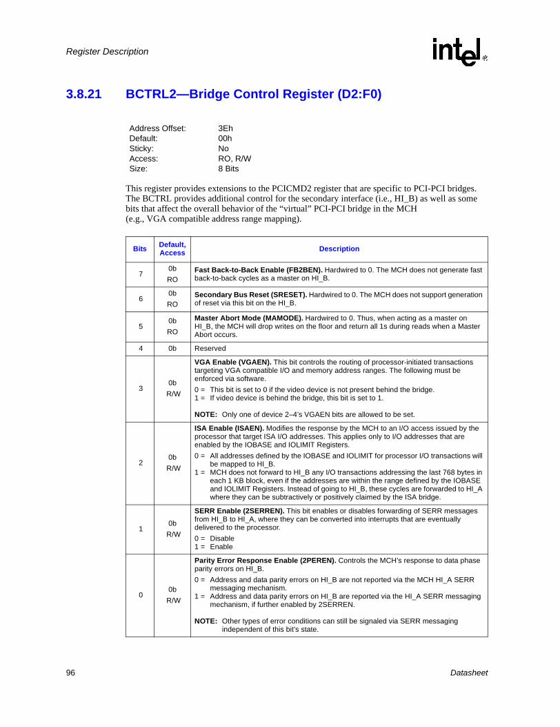
Register Description
3.8.21 BCTRL2—Bridge Control Register (D2:F0)
This register provides extensions to the PCICMD2 register that are specific to PCI-PCI bridges. The BCTRL provides additional control for the secondary interface (i.e., HI_B) as well as some bits that affect the overall behavior of the “virtual” PCI-PCI bridge in the MCH (e.g., VGA compatible address range mapping).
Address Offset: 3EhDefault: 00hSticky: NoAccess: RO, R/W Size: 8 Bits
Bits Default, Access Description
7 0bRO
Fast Back-to-Back Enable (FB2BEN). Hardwired to 0. The MCH does not generate fast back-to-back cycles as a master on HI_B.
6 0bRO
Secondary Bus Reset (SRESET). Hardwired to 0. The MCH does not support generation of reset via this bit on the HI_B.
5 0bRO
Master Abort Mode (MAMODE). Hardwired to 0. Thus, when acting as a master on HI_B, the MCH will drop writes on the floor and return all 1s during reads when a Master Abort occurs.
4 0b Reserved
3 0b
R/W
VGA Enable (VGAEN). This bit controls the routing of processor-initiated transactions targeting VGA compatible I/O and memory address ranges. The following must be enforced via software.0 = This bit is set to 0 if the video device is not present behind the bridge.1 = If video device is behind the bridge, this bit is set to 1.
NOTE: Only one of device 2–4’s VGAEN bits are allowed to be set.
2 0b
R/W
ISA Enable (ISAEN). Modifies the response by the MCH to an I/O access issued by the processor that target ISA I/O addresses. This applies only to I/O addresses that are enabled by the IOBASE and IOLIMIT Registers. 0 = All addresses defined by the IOBASE and IOLIMIT for processor I/O transactions will
be mapped to HI_B.1 = MCH does not forward to HI_B any I/O transactions addressing the last 768 bytes in
each 1 KB block, even if the addresses are within the range defined by the IOBASE and IOLIMIT Registers. Instead of going to HI_B, these cycles are forwarded to HI_A where they can be subtractively or positively claimed by the ISA bridge.
1 0b
R/W
SERR Enable (2SERREN). This bit enables or disables forwarding of SERR messages from HI_B to HI_A, where they can be converted into interrupts that are eventually delivered to the processor.0 = Disable1 = Enable
0 0b
R/W
Parity Error Response Enable (2PEREN). Controls the MCH’s response to data phase parity errors on HI_B. 0 = Address and data parity errors on HI_B are not reported via the MCH HI_A SERR
messaging mechanism. 1 = Address and data parity errors on HI_B are reported via the HI_A SERR messaging
mechanism, if further enabled by 2SERREN.
NOTE: Other types of error conditions can still be signaled via SERR messaging independent of this bit’s state.
96 Datasheet
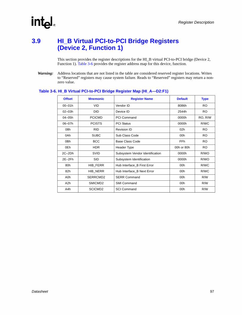
Register Description
3.9 HI_B Virtual PCI-to-PCI Bridge Registers (Device 2, Function 1)This section provides the register descriptions for the HI_B virtual PCI-to-PCI bridge (Device 2, Function 1). Table 3-6 provides the register address map for this device, function.
Warning: Address locations that are not listed in the table are considered reserved register locations. Writes to “Reserved” registers may cause system failure. Reads to “Reserved” registers may return a non-zero value.
Table 3-6. HI_B Virtual PCI-to-PCI Bridge Register Map (HI_A—D2:F1)
Offset Mnemonic Register Name Default Type
00–01h VID Vendor ID 8086h RO
02–03h DID Device ID 2544h RO
04–05h PCICMD PCI Command 0000h RO, R/W
06–07h PCISTS PCI Status 0000h R/WC
08h RID Revision ID 02h RO
0Ah SUBC Sub Class Code 00h RO
0Bh BCC Base Class Code FFh RO
0Eh HDR Header Type 00h or 80h RO
2C–2Dh SVID Subsystem Vendor Identification 0000h R/WO
2E–2Fh SID Subsystem Identification 0000h R/WO
80h HIB_FERR Hub Interface_B First Error 00h R/WC
82h HIB_NERR Hub Interface_B Next Error 00h R/WC
A0h SERRCMD2 SERR Command 00h R/W
A2h SMICMD2 SMI Command 00h R/W
A4h SCICMD2 SCI Command 00h R/W
Datasheet 97

Register Description
3.9.1 VID—Vendor Identification Register (D2:F1)
The VID Register contains the vendor identification number. This 16-bit register combined with the Device Identification Register uniquely identifies any PCI device.
3.9.2 DID—Device Identification Register (D2:F1)
.
Address Offset: 00hDefault: 8086hSticky: NoSMB Shadowed: YesAccess: RO Size: 16 Bits
Bits Default, Access Description
15:0 8086h
ROVendor Identification (VID). This register field contains the PCI standard identification for Intel (VID=8086h).
Address Offset: 02hDefault: 2544hSticky: NoSMB Shadowed: YesAccess: ROSize: 16 Bits
Bits Default, Access Description
15:0 2544h
RODevice Identification Number (DID). This is a 16-bit value assigned to the MCH Host-HI Bridge Function 1. The value is 2544h.
98 Datasheet

Register Description
3.9.3 PCICMD—PCI Command Register (D2:F1)
Since MCH Device 0 does not physically reside on a physical PCI bus portions of this register are not implemented.
3.9.4 PCISTS—PCI Status Register (D2:F1)
PCISTS is a 16-bit status register that reports the occurrence of error events on Device 0’s PCI interface. Bit 14 is read/write clear. All other bits are Read Only. Since MCH Device 0 does not physically reside on PCI_A many of the bits are not implemented.
Address Offset: 04hDefault: 0000hSticky: NoSMB Shadowed: YesAccess: R/WSize: 16 Bits
Bits Default, Access Description
15:9 00h Reserved
8 0b
R/W
SERR Enable (SERRE). This bit is global enable bit for Device 2 SERR messaging. 0 = Disable. SERR is not generated by the MCH for Device 2.1 = Enable. The MCH is enabled to generate SERR over HI_A for specific Device 2 error
conditions that are individually enabled in the ERRCMD register. The error status is reported in the ERRSTAT and PCISTS Registers.
7:0 00h Reserved
Address Offset: 06hDefault: 0000hSticky: NoSMB Shadowed: YesAccess: R/WCSize: 16 Bits
Bits Default, Access Description
15 0b Reserved
14 0b
R/WC
Signaled System Error (SSE). 0 = No signaled system error generated.1 = MCH Device 2 generated an SERR over HI_A for any enabled Device 2 error
condition. Device 2 error conditions are enabled in the PCICMD and ERRCMD Registers. Device 2 error flags are read/reset from the PCISTS or ERRSTAT Registers.
Note: Software sets this bit to 0 by writing a 1 to it.
13:0 000h Reserved
Datasheet 99

Register Description
3.9.5 RID—Revision Identification Register (D2:F1)
This register contains the revision number of the MCH Device 0.
3.9.6 SUBC—Sub-Class Code Register (D2:F1)
This register contains the Sub-Class Code for the MCH Device 0.
Address Offset: 08hDefault: See table belowSticky: NoSMB Shadowed: YesAccess: ROSize: 8 Bits
Bits Default, Access Description
7:0 02hRO
Revision Identification Number (RID). This is an 8-bit value that indicates the revision identification number for the MCH Device 0. This value should always be the same as the RID for device0, function 0.02h = A2 stepping
Address Offset: 0AhDefault: 00hSticky: NoSMB Shadowed: YesAccess: ROSize: 8 Bits
Bits Default, Access Description
7:0 00hRO
Sub-Class Code (SUBC). This is an 8-bit value that indicates the category of undefined. 00h = Undefined device.
100 Datasheet

Register Description
3.9.7 BCC—Base Class Code Register (D2:F1)
This register contains the Base Class Code of the MCH Device 2.
3.9.8 HDR—Header Type Register (D2:F1)
This register identifies the header layout of the configuration space. No physical register exists at this location.
Address Offset: 0BhDefault: FFhSticky: NoSMB Shadowed: YesAccess: ROSize: 8 Bits
Bits Default, Access Description
7:0 FFhRO
Base Class Code (BASEC). This is an 8-bit value that indicates the Base Class Code for the MCH. FFh =Non-defined device. Since this function is used for error conditions, it does not fall
into any other class.
Address Offset: 0EhDefault: 00h or 80h Sticky: NoSMB Shadowed: YesAccess: ROSize: 8 Bits
Bits Default, Access Description
7:0 00h or
80hRO
PCI Header (HDR). This read only field always returns 00h or 80h to indicate that the MCH is a multi-function device with standard header layout.
Datasheet 101

Register Description
3.9.9 SVID—Subsystem Vendor Identification Register (D2:F1)
This value is used to identify the vendor of the subsystem.
3.9.10 SID—Subsystem Identification Register (D2:F1)
This value is used to identify a particular subsystem.
Address Offset: 2C–2DhDefault: 0000hSticky: NoSMB Shadowed: YesAccess: R/WOSize: 16 Bits
Bits Default, Access Description
15:0 0000h R/WO
Subsystem Vendor ID (SUBVID). This field should be programmed during boot-up to indicate the vendor of the system board. After it has been written once, it becomes read only.
Address Offset: 2E–2FhDefault: 0000hSticky: NoSMB Shadowed: YesAccess: R/WOSize: 16 Bits
Bits Default, Access Description
15:0 0000h R/WO
Subsystem ID (SUBID). This field should be programmed during BIOS initialization. After it has been written once, it becomes read only.
102 Datasheet
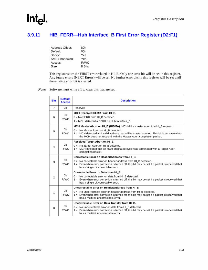
Register Description
3.9.11 HIB_FERR—Hub Interface_B First Error Register (D2:F1)
This register store the FIRST error related to HI_B. Only one error bit will be set in this register. Any future errors (NEXT Errors) will be set. No further error bits in this register will be set until the existing error bit is cleared.
Note: Software must write a 1 to clear bits that are set.
Address Offset: 80hDefault: 00hSticky: YesSMB Shadowed: YesAccess: R/WCSize: 8 Bits
Bits Default, Access Description
7 0b Reserved
60b
R/WC
MCH Received SERR From HI_B. 0 = No SERR from HI_B detected.1 = MCH detected a SERR on Hub Interface_B.
50b
R/WC
MCH Master Abort on HI_B (HIBMA). MCH did a master abort to a HI_B request. 0 = No Master Abort on HI_B detected.1 = MCH detected an invalid address that will be master aborted. This bit is set even when
the MCH does not respond with the Master Abort completion packet.
40b
R/WC
Received Target Abort on HI_B. 0 = No Target Abort on HI_B detected.1 = MCH detected that an MCH originated cycle was terminated with a Target Abort
completion packet.
30b
R/WC
Correctable Error on Header/Address from HI_B. 0 = No correctable error on header/address from HI_B detected.1 = Even when error correction is turned off, this bit may be set if a packet is received that
has a single bit correctable error.
20b
R/WC
Correctable Error on Data from HI_B. 0 = No correctable error on data from HI_B detected.1 = Even when error correction is turned off, this bit may be set if a packet is received that
has a single bit correctable error.
10b
R/WC
Uncorrectable Error on Header/Address from HI_B. 0 = No uncorrectable error on header/address from HI_B detected. 1 = Even when error correction is turned off, this bit may be set if a packet is received that
has a multi-bit uncorrectable error.
00b
R/WC
Uncorrectable Error on Data Transfer from HI_B. 0 = No uncorrectable error on data from HI_B detected.1 = Even when error correction is turned off, this bit may be set if a packet is received that
has a multi-bit uncorrectable error.
Datasheet 103

Register Description
3.9.12 HIB_NERR—Hub Interface_B Next Error Register (D2:F1)
The FIRST error related to HI_B will be stored in the HIB_FERR Register. This register store all future errors related to the HI_B. Multiple bits in this register may be set.
Note: Software must write a 1 to clear bits that are set.
Address Offset: 82hDefault: 00hSticky: YesSMB Shadowed: YesAccess: R/WCSize: 8 Bits
Bits Default, Access Description
7 0b Reserved
60b
R/WC
MCH Received SERR from HI_B. 0 = No SERR from HI_B received.1 = MCH received SERR from HI_B.
50b
R/WC
MCH Master Abort on HI_B (HIBMA). MCH did a Master Abort to a HI_B Request. 0 = No Master Abort on HI_B detected.1 = The MCH detected an invalid address that will be master aborted. This bit is set even
when the MCH does not respond with the Master Abort completion packet.
40b
R/WC
Received Target Abort on HI_B. 0 = No Target Abort detected.1 = The MCH has detected that an MCH originated cycle was terminated with a Target
Abort completion packet.
30b
R/WC
Correctable Error on Header/Address from HI_B. 0 = No correctable error on header/address from HI_B detected.1 = Even when error correction is turned off, this bit may be set if a packet is received
that has a single bit correctable error.
20b
R/WC
Correctable Error on Data from HI_B. 0 = No correctable error on data from HI_B detected.1 = Even when error correction is turned off, this bit may be set if a packet is received
that has a single bit correctable error.
10b
R/WC
Uncorrectable Error on Header/Address from HI_B. 0 = No uncorrectable error on header/address from HI_B detected.1 = Even when error correction is turned off, this bit may be set if a packet is received
that has a multi-bit uncorrectable error.
00b
R/WC
Uncorrectable Error on Data Transfer from HI_B. 0 = No uncorrectable error on data from HI_B detected.1 = Even when error correction is turned off, this bit may be set if a packet is received
that has a multi-bit uncorrectable error.
104 Datasheet

Register Description
3.9.13 SERRCMD2—SERR Command Register (D2:F1)
This register determines whether SERR will be generated when the associated flag is set in the FERR or NERR Register. When an error flag is set in the FERR or NERR Register, it can generate an SERR, SMI, or SCI when enabled in the SERRCMD, SMICMD, or SCICMD Registers, respectively. Only one message type can be enabled.
Address Offset: A0hDefault: 00hSticky: NoAccess: R/W Size: 8 Bits
Bits Default, Access Description
7:6 00b Reserved
50b
R/W
SERR on MCH Master Abort to a HI_B Request Enable. 0 = No SERR generation 1 = Generate SERR if bit 5 is set in HIB_FERR or HIB_NERR
40b
R/W
SERR on Received Target Abort on HI_B Enable. 0 = No SERR generation 1 = Generate SERR if bit 4 is set in HIB_FERR or HIB_NERR
30b
R/W
SERR on Correctable Error on Header/Address from HI_B Enable.0 = No SERR generation 1 = Generate SERR if bit 3 is set in HIB_FERR or HIB_NERR
20b
R/W
SERR on Correctable Error on Data from HI_B Enable.0 = No SERR generation 1 = Generate SERR if bit 2 is set in HIB_FERR or HIB_NERR
10b
R/W
SERR on Uncorrectable Error on Header/Address from HI_B Enable. 0 = No SERR generation 1 = Generate SERR if bit 1is set in HIB_FERR or HIB_NERR
00b
R/W
SERR on Uncorrectable Error on Data Transfer from HI_B Enable.0 = No SERR generation 1 = Generate SERR if bit 0 is set in HIB_FERR or HIB_NERR
Datasheet 105
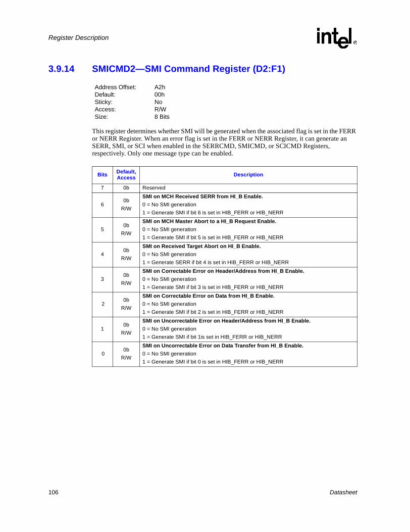
Register Description
3.9.14 SMICMD2—SMI Command Register (D2:F1)
This register determines whether SMI will be generated when the associated flag is set in the FERR or NERR Register. When an error flag is set in the FERR or NERR Register, it can generate an SERR, SMI, or SCI when enabled in the SERRCMD, SMICMD, or SCICMD Registers, respectively. Only one message type can be enabled.
Address Offset: A2hDefault: 00hSticky: NoAccess: R/WSize: 8 Bits
Bits Default, Access Description
7 0b Reserved
60b
R/W
SMI on MCH Received SERR from HI_B Enable. 0 = No SMI generation 1 = Generate SMI if bit 6 is set in HIB_FERR or HIB_NERR
50b
R/W
SMI on MCH Master Abort to a HI_B Request Enable. 0 = No SMI generation 1 = Generate SMI if bit 5 is set in HIB_FERR or HIB_NERR
40b
R/W
SMI on Received Target Abort on HI_B Enable. 0 = No SMI generation 1 = Generate SERR if bit 4 is set in HIB_FERR or HIB_NERR
30b
R/W
SMI on Correctable Error on Header/Address from HI_B Enable.0 = No SMI generation 1 = Generate SMI if bit 3 is set in HIB_FERR or HIB_NERR
20b
R/W
SMI on Correctable Error on Data from HI_B Enable.0 = No SMI generation 1 = Generate SMI if bit 2 is set in HIB_FERR or HIB_NERR
10b
R/W
SMI on Uncorrectable Error on Header/Address from HI_B Enable. 0 = No SMI generation 1 = Generate SMI if bit 1is set in HIB_FERR or HIB_NERR
00b
R/W
SMI on Uncorrectable Error on Data Transfer from HI_B Enable.0 = No SMI generation 1 = Generate SMI if bit 0 is set in HIB_FERR or HIB_NERR
106 Datasheet

Register Description
3.9.15 SCICMD2—SCI Command Register (D2:F1)
This register determines whether SCI will be generated when the associated flag is set in the FERR or NERR Register. When an error flag is set in the FERR or NERR Register, it can generate an SERR, SMI, or SCI when enabled in the ERRCMD, SMICMD, or SCICMD Registers, respectively. Only one message type can be enabled.
Address Offset: A4hDefault: 00hSticky: YesAccess: R/WSize: 8 Bits
Bits Default, Access Description
7 0b Reserved
60b
R/W
SCI on MCH Received SERR from HI_B Enable. 0 = No SCI generation 1 = Generate SCI if bit 6 is set in HIB_FERR or HIB_NERR
50b
R/W
SCI on MCH Master Abort to a HI_B Request Enable.0 = No SCI generation 1 = Generate SCI if bit 5 is set in HIB_FERR or HIB_NERR
40b
R/W
SCI on Received Target Abort on HI_B Enable.0 = No SCI generation 1 = Generate SCI if bit 4 is set in HIB_FERR or HIB_NERR
30b
R/W
SCI on Correctable Error on Header/Address from HI_B Enable.0 = No SCI generation 1 = Generate SCI if bit 3 is set in HIB_FERR or HIB_NERR
20b
R/W
SCI on Correctable Error on Data from HI_B Enable.0 = No SCI generation 1 = Generate SCI if bit 2 is set in HIB_FERR or HIB_NERR
10b
R/W
SCI on Uncorrectable Error on Header/Address from HI_B Enable. 0 = No SCI generation 1 = Generate SCI if bit 1is set in HIB_FERR or HIB_NERR
00b
R/W
SCI on Uncorrectable Error on Data Transfer from HI_B Enable.0 = No SCI generation 1 = Generate SCI if bit 0 is set in HIB_FERR or HIB_NERR
Datasheet 107
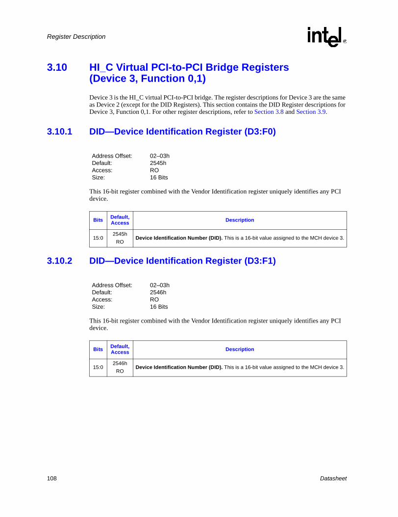
Register Description
3.10 HI_C Virtual PCI-to-PCI Bridge Registers (Device 3, Function 0,1)Device 3 is the HI_C virtual PCI-to-PCI bridge. The register descriptions for Device 3 are the same as Device 2 (except for the DID Registers). This section contains the DID Register descriptions for Device 3, Function 0,1. For other register descriptions, refer to Section 3.8 and Section 3.9.
3.10.1 DID—Device Identification Register (D3:F0)
This 16-bit register combined with the Vendor Identification register uniquely identifies any PCI device.
3.10.2 DID—Device Identification Register (D3:F1)
This 16-bit register combined with the Vendor Identification register uniquely identifies any PCI device.
Address Offset: 02–03hDefault: 2545hAccess: RO Size: 16 Bits
Bits Default, Access Description
15:02545h
RODevice Identification Number (DID). This is a 16-bit value assigned to the MCH device 3.
Address Offset: 02–03hDefault: 2546hAccess: RO Size: 16 Bits
Bits Default, Access Description
15:02546h
RODevice Identification Number (DID). This is a 16-bit value assigned to the MCH device 3.
108 Datasheet

Register Description
3.11 HI_D Virtual PCI-to-PCI Bridge Registers (Device 4, Function 0,1)Device 4 is the HI_D virtual PCI-to-PCI bridge. The register descriptions for Device 4 are the same as Device 2 (except for the DID Registers). This section contains the DID Register descriptions for Device 4, Function 0,1. For other register descriptions, refer to Section 3.8 and Section 3.9.
3.11.1 DID—Device Identification Register (D4:F0)
This 16-bit register combined with the Vendor Identification Register uniquely identifies any PCI device.
3.11.2 DID—Device Identification Register (D4:F1)
This 16-bit register combined with the Vendor Identification Register uniquely identifies any PCI device. Writes to this register have no effect.
Address Offset: 02–03hDefault: 2547hAccess: RO Size: 16 Bits
Bits Default, Access Description
15:02547h
RODevice Identification Number (DID). This is a 16-bit value assigned to the MCH device 4.
Address Offset: 02–03hDefault: 2548hAccess: RO Size: 16 Bits
Bits Default, Access Description
15:02548h
RODevice Identification Number (DID). This is a 16-bit value assigned to the MCH device 4.
Datasheet 109

Register Description
This page is intentionally left blank.
110 Datasheet

System Address Map
System Address Map 4
A system based on the E7500 chipset supports 16 GB of host-addressable memory space and 64 KB + 3 bytes of host-addressable I/O space. The I/O and memory spaces are divided by system configuration software into regions. The memory ranges are useful either as system memory or as specialized memory, while the I/O regions are used solely to control the operation of devices in the system.
4.1 System Memory SpacesThere are four basic regions of memory in the system:
• High Memory Range. Memory above 4 GB. This memory range is for additional main memory (1_0000_0000h to 3_FFFF_FFFFh).
• Memory between 1 MB and the Top of Low Memory (TOLM) Register. This is a main memory address range (0_0100_0000h to TOLM).
• Memory between the TOLM Register and 4 GB. This range is used for mapping APIC and Hub Interface_A–D. Programmable non-overlapping I/O windows can be mapped to this area.
• DOS Compatible memory area. Memory below 1 MB (0_0000_0000h to 0_0009_FFFFh).
Figure 4-1. System Address Map
These address ranges are always mapped to system memory, regardless of the system configuration. Memory may be allocated from the main memory segment 0_0100_0000h to TOLM for use by System Management Mode (SMM) hardware and software. The top of main memory is defined by the Top of Low Memory (TOLM) Register. Note that the address of the highest 64 MB quantity of valid memory in the system is placed into the DRB7 Register. For systems with a total DRAM space and PCI memory-mapped space of less than 4 GB, this value will be the same as the one programmed into the TOLM Register. For other memory configurations, the two are unlikely to be the same, since the PCI configuration portion of the BIOS software will program the TOLM
DOS Legacy AddressRange
Main MemoryAddress Range
PCI Memory AddressRange
Top of LowMemory
1 MB
4 GB
Hub Interface_A–D I/OAperture
APICs
Independently ProgrammableNon-overlapping Windows
Additional MainMemory Address
Range
16 GB
Datasheet 111

System Address Map
Register to the maximum value that is less than 4 GB and also allows enough room for all populated PCI devices. Figure 4-2 shows the segments within the extended memory segment (1 MB to 4 GB).
Figure 4-2. Detailed Extended Memory Range Address Map
= Main Memory Region
= Optional Main Memory Region
1_0000_0000 (4 GB)
FEF0_0000
FEE0_0000
FED0_0000
Top of Low Memory (TOLM)
FEC0_0000
FEC8_0000
FF00_0000
100A_0000
100C_0000
00F0_0000 (15 MB)
0100_0000 (16 MB)
0010_0000 (1 MB)
TEM - TSEG
High BIOS, Optionalextended SMRAM
dd 3
ISA Hole (optional)
Extended SMRAMSpace
Local APIC Space
Hub Interface_B–D,I/O APIC Space
Hub interface_A,I/O APIC Space
Hub Interface_B–DWindows
Hub Interface_A(always)
Hub Interface_A(always)
112 Datasheet

System Address Map
4.1.1 VGA and MDA Memory SpacesVideo cards use these legacy address ranges to map a frame buffer or a character-based video buffer. The address ranges in this memory space are:
• VGAA 0_000A_0000h to 0_000A_FFFFh
• MDA 0_000B_0000h to 0_000B_7FFFh
• VGAB 0_000B_8000h to 0_000B_FFFFh
By default, accesses to these ranges are forwarded to Hub Interface_A. However, if the VGA_EN bit is set in the BCTRL 2–4 configuration registers, then transactions within the VGA and MDA spaces are sent to Hub Interface_B, C, D, respectively.
Note: The VGA_EN bit may be set in one and only one of the BCTRL Registers. Software must not set more than one of the VGA_EN bits.
If the configuration bit MCHCFG.MDAP is set, accesses that fall within the MDA range will be sent to Hub Interface_A without regard for the VGAEN bits. Legacy support requires the ability to have a second graphics controller (monochrome) in the system. In a E7500 chipset system, accesses in the standard VGA range are forwarded to Hub Interface_B, C, D (depending on configuration bits). Since the monochrome adapter may be on the HI_A/PCI (or ISA) bus, the MCH must decode cycles in the MDA range and forward them to Hub Interface_A. This capability is controlled by a configuration bit (MDAP bit). In addition to the memory range B0000h to B7FFFh, the MCH decodes I/O cycles at 3B4h, 3B5h, 3B8h, 3B9h, 3BAh and 3BFh and forwards them to Hub Interface_A.
An optimization allows the system to reclaim the memory displaced by these regions. When SMM memory space is enabled by SMRAM.G_SMRAME and either the SMRAM.D_OPEN bit is set or the system bus receives an SMM-encoded request for code (not data), the transaction is steered to system memory rather than HI_A. Under these conditions, both of the VGAEN bits and the MDAP bit are ignored.
Datasheet 113

System Address Map
4.1.2 PAM Memory SpacesThe address ranges in this space are:
• PAMC0 0_000C_0000 to 0_000C_3FFF
• PAMC4 0_000C_4000 to 0_000C_7FFF
• PAMC8 0_000C_8000 to 0_000C_BFFF
• PAMCC 0_000C_C000 to 0_000C_FFFF
• PAMD0 0_000D_0000 to 0_000D_3FFF
• PAMD4 0_000D_4000 to 0_000D_7FFF
• PAMD8 0_000D_8000 to 0_000D_BFFF
• PAMDC 0_000D_C000 to 0_000D_FFFF
• PAME0 0_000E_0000 to 0_000E_3FFF
• PAME4 0_000E_4000 to 0_000E_7FFF
• PAME8 0_000E_8000 to 0_000E_BFFF
• PAMEC 0_000E_C000 to 0_000E_FFFF
• PAMF0 0_000F_0000 to 0_000F_FFFF
The 256 KB PAM region is divided into three parts:
• ISA expansion region: 128 KB area between 0_000C_0000h and 0_000D_FFFFh
• Extended BIOS region: 64 KB area between 0_000E_0000h and 0_000E_FFFFh,
• System BIOS region: 64 KB area between 0_000F_0000h and 0_000F_FFFFh.
The ISA expansion region is divided into eight, 16-KB segments. Each segment can be assigned one of four read/write states: read-only, write-only, read/write, or disabled. Typically, these blocks are mapped through the MCH and are subtractively decoded to ISA space.
The extended system BIOS region is divided into four, 16-KB segments. Each segment can be assigned independent read and write attributes so it can be mapped either to main memory or to Hub Interface_A. Typically, this area is used for RAM or ROM.
The system BIOS region is a single, 64-KB segment. This segment can be assigned read and write attributes. It is by default (after reset) read/write disabled and cycles are forwarded to Hub Interface_A. By manipulating the read/write attributes, the MCH can shadow BIOS into the main memory.
Note that the PAM region can be accessed by Hub Interface_A–D. All reads or writes from any Hub Interface that hits the PAM area is sent to main memory. If the system is setup so that there are Hub Interface accesses to the PAM regions, then the PAM region being accessed must be programmed to be both readable and writable by the processor. If the accessed PAM region is programmed for either reads or writes to be forwarded to Hub Interface_A, and there are Hub Interface accesses to that PAM, the system may fault.
114 Datasheet

System Address Map
4.1.3 ISA Hole Memory Space
BIOS software may optionally open a “window” between 15 MB and 16 MB (0_00F0_0000 to 0_00FF_FFFF) that relays transactions to Hub Interface_A instead of completing them with a system memory access. This window is opened with the FDHC.HEN configuration field.
4.1.4 I/O APIC Memory SpaceThe I/O APIC spaces are used to communicate with I/O APIC interrupt controllers that may be populated on Hub Interface_A through Hub Interface_D. Since it is difficult to relocate an interrupt controller using plug-and-play software, fixed address decode regions have been allocated for them. The address ranges are:
• I/OAPIC0 (HI_A) 0_FEC0_0000h to 0_FEC7_FFFFh
• I/OAPIC1 (HI_B) 0_FEC8_0000h to 0_FEC8_0FFFh
• I/OAPIC2 (HI_C) 0_FEC8_1000h to 0_FEC8_1FFFh
• I/OAPIC3 (HI_D) 0_FEC8_2000h to 0_FEC8_2FFFh
Processor accesses to the I/OAPIC0 region are always sent to Hub Interface_A. Processor accesses to the I/OAPIC1 region are always sent to Hub Interface_B and so on.
4.1.5 System Bus Interrupt Memory SpaceThe system bus interrupt space (0_FEE0_0000h to 0_FEEF_FFFFh) is the address used to deliver interrupts to the system bus. Any device on Hub Interface_A–D may issue a double-word memory write to 0FEEx_xxxxh. The MCH will forward this memory write along with the data to the system bus as an Interrupt Message Transaction. The MCH terminates the system bus transaction by providing the response and asserting TRDY#. This memory write cycle does not go to DRAM.
The processors may also use this region to send inter-processor interrupts (IPI) from one processor to another.
4.1.6 Device 2 Memory and Prefetchable MemoryPlug-and-play software configures the HI_B memory window to provide enough memory space for the devices behind this PCI-to-PCI Bridge. Accesses that have addresses that fall within this window are decoded and forwarded to Hub Interface_B for completion. The address ranges are:
• M2 MBASE2 to MLIMIT2
• PM2 PMBASE2 to PMLIMIT2
Note that these registers must be programmed with values that place the Hub Interface_B memory space window between the value in the TOLM Register and 4 GB. In addition, neither region should overlap with any other fixed or relocatable area of memory.
Datasheet 115

System Address Map
4.1.7 Device 3 Memory and Prefetchable MemoryPlug-and-play software configures the Hub Interface_C memory window to provide enough memory space for the devices behind this PCI-to-PCI Bridge. Accesses that have addresses that fall within this window are decoded and forwarded to Hub Interface_C for completion.
• M3 MBASE3 to MLIMIT3
• PM3 PMBASE3 to PMLIMIT3
Note that these registers must be programmed with values that place the Hub Interface_C memory space window between the value in the TOLM Register and 4 GB. In addition, neither region should overlap with any other fixed or relocatable area of memory.
4.1.8 Device 4 Memory and Prefetchable MemoryPlug-and-play software configures the Hub Interface_D memory window to provide enough memory space for the devices behind this PCI-to-PCI Bridge. Accesses that have addresses that fall within this window are decoded and forwarded to Hub Interface_D for completion.
• M4 MBASE4 to MLIMIT4
• PM4 PMBASE4 to PMLIMIT4
Note that these registers must be programmed with values that place the Hub Interface_D memory space window between the value in the TOLM Register and 4 GB. In addition, neither region should overlap with any other fixed or relocatable area of memory.
4.1.9 HI_A Subtractive DecodeAll accesses that fall between the value programmed into the TOLM Register and 4 GB (i.e., TOLM and 4 GB) are subtractively decoded and forwarded to Hub Interface_A if they do not decode to a space that corresponds to another device.
4.1.10 Main Memory AddressesThe high memory and extended memory address regions are together called main memory. Main memory is composed of address segments that refer to SDRAM system memory. Main memory addresses are mapped to SDRAM channels, devices, banks, rows, and columns in different ways depending upon the type of memory being used and the density or organization of the memory. Refer to Section 1.4.2 for supported DIMM configurations.
116 Datasheet

System Address Map
4.2 I/O Address SpaceThe MCH does not support the existence of any other I/O devices on the system bus. The MCH generates Hub Interface_A–D bus cycles for all processor I/O accesses. The MCH contains two internal registers in the processor I/O space, Configuration Address Register (CONF_ADDR) and the Configuration Data Register (CONF_DATA). These locations are used to implement the configuration space access mechanism and are described in Device Configuration Registers section.
The processor allows 64 KB + 3 bytes to be addressed within the I/O space. The MCH propagates the processor I/O address without any translation to the targeted destination bus. Note that the upper three locations can be accessed only during I/O address wrap-around when signal A16# is asserted on the system bus. A16# is asserted on the system bus whenever a DWord I/O access is made from address 0FFFDh, 0FFFEh, or 0FFFFh. In addition, A16# is asserted when software attempts a two bytes I/O access from address 0FFFFh.
The I/O accesses (other than ones used for configuration space access) are forwarded normally to Hub Interface_A–D. All I/O cycles receive a Defer Response. The MCH never posts an I/O write.
The MCH never responds to I/O or configuration cycles initiated on any of the hub interfaces. Hub interface transactions requiring completion are terminated with “master abort” completion packets on the hub interfaces. Hub interface I/O write transactions not requiring completion are dropped.
4.3 SMM Space
4.3.1 System Management Mode (SMM) Memory Range The E7500 chipset supports the use of main memory as System Management RAM (SMM RAM), which enables the use of System Management Mode. The MCH supports three SMM options:
• Compatible SMRAM (C_SMRAM)
• High Segment (HSEG)
• Top of Memory Segment (TSEG).
System Management RAM space provides a memory area that is available for the SMI handlers and code and data storage. This memory resource is normally hidden from the system operating system so the processor has immediate access to this memory space upon entry to SMM. The MCH provides three SMRAM options:
• Below 1-MB option that supports compatible SMI handlers.
• Above 1-MB option that allows new SMI handlers to execute with write-back cacheable SMRAM.
• Optional larger write-back cacheable TSEG area from 128 KB to 1 MB in size above 1 MB that is reserved below the 4 GB in system DRAM memory space. The above 1-MB solutions require changes to compatible SMRAM handler code to properly execute above 1 MB.
Datasheet 117

System Address Map
4.3.2 TSEG SMM Memory Space
The TSEG SMM space (TOLM – TSEG to TOLM) allows system management software to partition a region of main memory just below the top of low memory (TOLM) that is accessible only by system management software. This region may be 128 KB, 256 KB, 512 KB, or 1 MB in size, depending upon the ESMRAMC.TSEG_SZ field. This space must be below 4 GB, so it is below TOLM and not the top of physical memory, SMM memory is globally enabled by SMRAM.G_SMRAME. Requests may access SMM system memory when either SMM space is open (SMRAM.D_OPEN) or the MCH receives an SMM code request on its system bus. To access the TSEG SMM space, TSEG must be enabled by ESMRAMC.T_EN. When all of these conditions are met, a system bus access to the TSEG space (between TOLM–TSEG and TOLM) is sent to system memory. When the high SMRAM is not enabled or if the TSEG is not enabled, memory requests from all interfaces are forwarded to system memory. When the TSEG SMM space is enabled, and an agent attempts a non-SMM access to TSEG space, then the transaction is specially terminated.
Hub interface originated accesses are not allowed to SMM space.
4.3.3 High SMM Memory SpaceThe HIGHSMM space (0_FEDA_0000h to 0_FEDB_FFFFh) allows cacheable access to the compatible SMM space by remapping valid SMM accesses between 0_FEDA_0000h and 0_FEDB_FFFFh to accesses between 0_000A_0000h and 0_000B_FFFFh. The accesses are remapped when SMRAM space is enabled; an appropriate access is detected on the system bus, and when ESMRAMC.H_SMRAME allows access to high SMRAM space. SMM memory accesses from any hub interface are specially terminated: reads are provided with the value from address 0 while writes are ignored entirely.
4.3.4 SMM Space RestrictionsWhen any of the following conditions are violated, the results of SMM accesses are unpredictable and may cause undesirable system behavior:
1. The Compatible SMM space must not be setup as cacheable.
2. Both D_OPEN and D_CLOSE must not be set to 1 at the same time.
3. When TSEG SMM space is enabled, the TSEG space must not be reported to the operating system as available DRAM. This is a BIOS responsibility.
118 Datasheet

System Address Map
4.3.5 SMM Space DefinitionSMM space is defined by its addressed SMM space and its DRAM SMM space. The addressed SMM space is defined as the range of bus addresses used by the processor to access SMM space. DRAM SMM space is defined as the range of physical DRAM memory locations containing the SMM code. SMM space can be accessed at one of three transaction address ranges: Compatible, High, and TSEG. The Compatible and TSEG SMM space is not remapped and, therefore, the addressed and DRAM SMM space is the same address range. Since the High SMM space is remapped, the addressed and DRAM SMM space is a different address range. Note that the High DRAM space is the same as the Compatible Transaction Address space. Table 4-1 describes three unique address ranges:
• Compatible Transaction Address
• High Transaction Address
• TSEG Transaction Address
Table 4-1. SMM Address Range
NOTES:1. High SMM: This is different than in previous chipsets. In previous chipsets the High segment was the 384 KB
region from A_0000h to F_FFFFh. However, C_0000h to F_FFFFh was not practically useful so it is deleted in the MCH.
2. TSEG SMM: This is different than in previous chipsets. In previous chipsets the TSEG address space was offset by 256 MB to allow for simpler decoding and the TSEG was remapped to just under the TOLM. In the MCH the TSEG region is not offset by 256 MB and it is not remapped.
SMM Space Enabled Transaction Address Space DRAM Space
Compatible A0000h to BFFFFh A0000h to BFFFFh
High 0FEDA0000h to 0FEDBFFFFh A0000h to BFFFFh
TSEG (TOLM–TSEG_SZ) to TOLM (TOLM–TSEG_SZ) to TOLM
Datasheet 119

System Address Map
4.4 Memory Reclaim BackgroundThe following memory-mapped I/O devices are typically located below 4 GB:
• High BIOS
• HSEG
• XAPIC
• Local APIC
• System Bus Interrupts
• HI_B, HI_C, HI_D BARs
In previous generation MCHs, the physical main memory overlapped by the logical address space allocated to these memory-mapped I/O devices was unusable. In server systems the memory allocated to memory-mapped I/O devices could easily exceed 1 GB. The result is that a large amount of physical memory would not be usable.
The MCH provides the capability to re-claim the physical memory overlapped by the memory mapped I/O logical address space. The MCH re-maps physical memory from the Top of Low Memory (TOLM) boundary up to the 4 GB boundary (or DRB7 if less than 4 GB) to an equivalent sized logical address range located just above the top of physical memory
4.4.1 Memory Re-MappingAn incoming address (referred to as a logical address) is checked to see if it falls in the memory re-map window. The bottom of the re-map window is defined by the value in the REMAPBASE Register. The top of the re-map window is defined by the value in the REMAPLIMIT Register. An address that falls within this window is remapped to the physical memory starting at the address defined by the TOLM Register.
120 Datasheet

Reliability, Availability, Serviceability, Usability, and Manageability (RASUM)
Reliability, Availability, Serviceability, Usability, and Manageability (RASUM) 5
The E7500 chipset-based platforms provide the RASUM (Reliability, Availability, Serviceability, Usability, and Manageability) features required for entry-level and mid-range servers. These features include: Chipkill technology ECC for memory, ECC for all high-performance I/O, out-of-band manageability through SMBus target interfaces on all major components, memory scrubbing and auto-initialization, processor thermal monitoring, and hot-plug PCI.
5.1 DRAM ECCThe ECC used for DRAM provides chipkill technology protection for x4 SDRAMs. DRAMS that are x8 use the same algorithm but will not have chipkill technology protection, since at most only four bits can be corrected with this ECC.
5.2 DRAM ScrubbingA special DRAM scrub algorithm will walk through all of main memory doing reads followed by writes back to the same location. Correctable errors found by the read are corrected and then the good data is written back to DRAM. A write is done in all cases, whether there were errors or not. This looks like a read-modify-write of 0 bytes to the system. The scrub unit starts at address 0 upon reset. Periodically, the unit will scrub one line and then increment the address counter by 64 bytes or one line. A 16-GB memory array would be completely scrubbed in approximately one day.
5.3 DRAM Auto-InitializationThe DRAM Auto-initialization algorithms initialize memory at reset to ensure that all lines have valid ECC.
5.4 SMBus AccessThe processor will be able to access all configuration registers through host configuration cycles. Access via SMBus will be R/W to a shadowed set of the RASUM registers in the MCH, and read-only to all non-RASUM registers in the MCH. The SMBus can not use the MCH’s SM-port to access any registers outside the MCH. The P64H2 and ICH3-S each have their own SMBus target port. A test mode will be provided to allow the processor to access the shadowed register set. Shadowing the RASUM registers ensures that BIOS code and system management ASIC firmware code can execute independently, without interference or synchronization efforts. PCI legacy registers associated with error reporting will not deviate from prior implementations. SMBus will have read-only access to the PCI legacy registers.
Datasheet 121

Reliability, Availability, Serviceability, Usability, and Manageability (RASUM)
This page is intentionally left blank.
122 Datasheet

Electrical Characteristics
Electrical Characteristics 6
This chapter provides the absolute maximum ratings, thermal characteristics, and DC characteristics for the MCH.
6.1 Absolute Maximum Ratings
Warning: Stressing the device beyond the “Absolute Maximum Ratings” may cause permanent damage. These are stress ratings only. Operating beyond the “operating conditions” is not recommended and extended exposure beyond “operating conditions” may affect reliability.
6.2 Thermal CharacteristicsThe MCH is designed for operation at die temperatures between 0 °C and 110 °C. The thermal resistance of the package is given in Table 6-2.
NOTES:1. Typical value measured in accordance with EIA/JESD 51-2 testing standard.2. 1 meter/second is equivalent to 196.9 linear feet/minute
Table 6-1. Absolute Maximum Ratings
Symbol Parameter Min Max Unit Notes
Tstorage Storage Temperature -55 150 °C
VCC_MCH 1.2 V Supply Voltage with respect to VSS -0.38 2.1 V
VTT_AGTL Supply Voltage input with respect to VSS -0.38 2.1 V
VDD_DDR DDR Buffer Supply Voltage 2 3 V
Table 6-2. MCH Package Thermal Resistance
ParameterAir Flow
No Air Flow (0 Meter/Second) 1.0 Meter/Second 2
Psijt (°C/Watt) 1 0.5 1.0
Thetaja (°C/Watt) 1 13.0 11.2
Datasheet 123

Electrical Characteristics
6.3 Power Characteristics
NOTES:1. TDP Typ is the Thermal Design Power (11.6 W) and it is the estimated maximum possible expected power
generated in a component by a realistic application. It is based on extrapolations in both hardware and software technology over the life of the component. It does not represent the expected power generated by a power virus. Studies by Intel indicate that no useful application will cause thermally significant power dissipation exceeding the TDP Typ specification, although it is possible to concoct higher power synthetic workloads as reflected in the TDP Max specification.
Table 6-3. Thermal Power Dissipation (VCC1_2 = 1.2 V ±5%)
Symbol Parameter Min Typ Max Unit Notes
PMCH Thermal Power Dissipation for MCH 11.6 15.6 W 1
Table 6-4. DC Characteristics Functional Operating Range (VCC1_2 = 1.2 V ±5%)
Symbol Parameter Min Typ Max Unit Notes
ICC 1.2 V Plumas Core and HI 3.1 A
IVTT 1.55 V AGTL 2.0 A
Idd_DDR 2.5 V VDD DDR (2 channel) 7 A
124 Datasheet

Electrical Characteristics
6.4 I/O Interface Signal GroupingsThe signal description includes the type of buffer used for the particular signal:
• AGTL+ Open Drain AGTL+ interface signal. Refer to the AGTL+ I/O Specification for complete details. The MCH integrates AGTL+ termination resistors.
• CMOS 1.2 V CMOS buffers.
• DDR DDR SDRAM signaling Interface
NOTES:1. x = A, B DDR channel
Table 6-5. Signal Groups System Bus Interface
Signal Group Signal Type Signals Notes
(a) AGTL+ I/O
AP[1:0]#, ADS#, BNR#, DBSY#, DP[3:0]#, DRDY#, HA[35:3]#, HADSTB[1:0] #, HD[63:0] #, HDSTBP[3:0]#, HDSTBN[3:0]#, HIT#, HITM#, HREQ[4:0]#, BREQ0#, DBI[3;0]#
(b) AGTL+ Output BPRI#, CPURST#, DEFER#, HTRDY#, RS [2:0]#, RSP#
(c) AGTL+ Input HLOCK#, XERR#
(d) Host Reference Voltage HDVREF[3:0], HAVREF[1:0], HCCVREF
(e) Host Voltage Swing HXSWING, HYSWING
(f) Host Compensation HXRCOMP, HYRCOMP
(g) CLK Inputs HCLKINN, HCLKINP
(h) AGTL + Termination Voltage VTT
Table 6-6. Signal Groups DDR Interface
Signal Group Signal Type Signals Notes
(i) DDR I/O DQ_x [63:0], CB_x [7:0], DQS_x [17:0] 1
(j) DDR OutputCMDCLK_x [3:0], CMDCLK_x#[3:0], MA_x [12:0], BA_x [1:0], RAS_x#, CAS_x#, WE_x#, CS_x [7:0]#, CKE_x, RCVENOUT_x#
1
(k) DDR Input RCVENIN_x# 1
(l) DDR Compensation CMOS I/O DDRCOMP_x 1
(m) DDR Compensation for impedance control DDRCVOH_x, DDRCVOL_x 1
(n) DDR Reference Voltage DDRVREF_x [5:0] 1
Datasheet 125

Electrical Characteristics
NOTES:1. x = B, C, D (referencing Hub Interface_B–D). 2. CLK66 is shared on HI 1.5 and HI 2.0
NOTES: 1. CLK66 is shared on HI 1.5 and HI 2.0
Table 6-7. Signal Groups Hub Interface 2.0 (HI_B–D)Signal Group Signal Type Signals Notes
(o) Hub Interface CMOS I/O HI_x [21:0], PSTRBF_x, PSTRBS_x 1
(p) Hub Interface CMOS Input Clock CLK66 2
(q) Hub Interface Reference Voltage Input HIVREF_x 1
(r) Hub Interface Voltage Swing HISWNG_x 1
(s) Hub Interface Compensation CMOS I/O HIRCOMP_x 1
Table 6-8. Signal Groups Hub Interface 1.5 (HI_A)Signal Group Signal Type Signals Notes
(t) Hub Interface CMOS I/O HI_A [11:0], HI_STBF, HI_STBS
(u) Hub Interface CMOS Input Clock CLK66 1
(v) Hub Interface Reference Voltage Input HIVREF_A
(w) Hub Interface Voltage Swing HISWNG_A
(x) Hub Interface Compensation CMOS I/O HIRCOMP_A
Table 6-9. Signal Groups SMBusSignal Group Signal Type Signals Notes
(y) SMBus I/O Buffer SMB_CLK, SMB_DATA
Table 6-10. Signal Groups Reset and MiscellaneousSignal Group Signal Type Signals Notes
(z) Miscellaneous CMOS Input RSTIN#, PWRGOOD, XORMODE#
126 Datasheet

Electrical Characteristics
6.5 DC Characteristics
Table 6-11. Operating Condition Supply Voltage (VCC1_2 = 1.2 V ±5%)
Symbol Signal Group Parameter Min Nom Max Unit Notes
VTT (h) Host AGTL+ Termination Voltage 1.15 1.3 1.45 V
VDD_DDR DDR Buffer Voltage 2.3 2.5 2.7 V
VCC_MCH 1.2 V Supply voltage 1.14 1.2 1.26 V
Table 6-12. System Bus Interface (VCC1_2 = 1.2 V ±5%)
Symbol Signal Group Parameter Min Nom Max Unit Notes
VIL_H (a), (c) Host AGTL+ Input Low Voltage (2/3 x VTT) – 0.1GTLREF
V
VIH_H (a), (c) Host AGTL+ Input High Voltage (2/3 x VTT) + 0.1GTLREF V
VOL_H (a), (b) Host AGTL+ Output Low Voltage 1/3 x VTT (1/3 x VTT) + 0.1GTLREF V
VOH_H (a), (b) Host AGTL+ Output High Voltage VTT–0.1 VTT V
RTT Host termination Resistance 46 50 54 W
IOL_H (a), (b) Host AGTL+ Output Low Leakage (2/3 x VTTmax) / RTT min A
IL_H (a), (c) Host AGTL+ Input Leakage Current 10 µA
CPAD (a), (c) Host AGTL+ Input Capacitance 1 3.5 pF
CCVREF (d) Host Common clock Reference Voltage 2/3 x VTT V
HxVREF (d) Host Address and Data Reference Voltage 2/3 x VTT V
HXSWNG, HYSWNG (e) Host Compensation Reference
Voltage 1/3 x VTT V
Datasheet 127
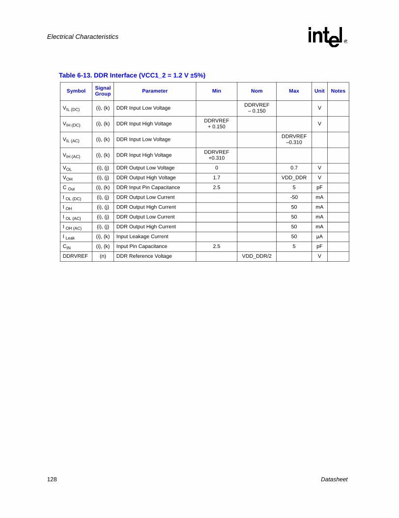
Electrical Characteristics
Table 6-13. DDR Interface (VCC1_2 = 1.2 V ±5%)
Symbol Signal Group Parameter Min Nom Max Unit Notes
VIL (DC) (i), (k) DDR Input Low Voltage DDRVREF – 0.150 V
VIH (DC) (i), (k) DDR Input High Voltage DDRVREF + 0.150 V
VIL (AC) (i), (k) DDR Input Low Voltage DDRVREF–0.310
VIH (AC) (i), (k) DDR Input High Voltage DDRVREF +0.310
VOL (i), (j) DDR Output Low Voltage 0 0.7 V
VOH (i), (j) DDR Output High Voltage 1.7 VDD_DDR V
C Out (i), (k) DDR Input Pin Capacitance 2.5 5 pF
I OL (DC) (i), (j) DDR Output Low Current -50 mA
I OH (i), (j) DDR Output High Current 50 mA
I OL (AC) (i), (j) DDR Output Low Current 50 mA
I OH (AC) (i), (j) DDR Output High Current 50 mA
I Leak (i), (k) Input Leakage Current 50 µA
CIN (i), (k) Input Pin Capacitance 2.5 5 pF
DDRVREF (n) DDR Reference Voltage VDD_DDR/2 V
128 Datasheet
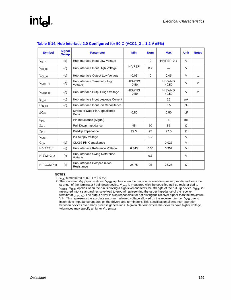
Electrical Characteristics
NOTES:1. VOL is measured at IOUT = 1.0 mA2. There are two VOH specifications. VOHT applies when the pin is in receive (terminating) mode and tests the
strength of the terminator / pull-down device. VOHT is measured with the specified pull-up resistor tied to VDDHI. VOHD applies when the pin is driving a high level and tests the strength of the pull-up device. VOHD is measured into a standard resistive load to ground representing the target impedance of the receiver terminator (ZTARG). The output driver is also responsible for not driving the receiver higher than the maximum VIH. This represents the absolute maximum allowed voltage allowed on the receiver pin (i.e., VOH due to incomplete impedance updates on the drivers and terminator). This specification allows inter-operation between devices over many process generations. A given platform where the devices have higher voltage tolerances may specify a higher VIH (max).
Table 6-14. Hub Interface 2.0 Configured for 50 Ω (VCC1_2 = 1.2 V ±5%)
Symbol Signal Group Parameter Min Nom Max Unit Notes
VIL_HI (o) Hub Interface Input Low Voltage 0 HIVREF–0.1 V
VIH_HI (o) Hub Interface Input High Voltage HIVREF+0.1 0.7 — V
VOL_HI (o) Hub Interface Output Low Voltage -0.03 0 0.05 V 1
VOHT_HI (o) Hub Interface Terminator High Voltage
HISWNG–0.50
HISWNG+0.50 V 2
VOHD_HI (o) Hub Interface Output High Voltage HISWNG–0.50
HISWNG+0.50 V 2
IIL_HI (o) Hub Interface Input Leakage Current 25 µA
CIN_HI (o) Hub Interface Input Pin Capacitance 3.5 pF
∆CINStrobe to Data Pin Capacitance Delta -0.50 0.50 pF
LPIN Pin Inductance (Signal) 5 nH
ZPD Pull-Down Impedance 45 50 55 Ω
ZPU Pull-Up Impedance 22.5 25 27.5 Ω
VCCP I/O Supply Voltage 1.2 V
CClk (p) CLK66 Pin Capacitance 0.025 V
HIVREF_x (q) Hub Interface Reference Voltage 0.343 0.35 0.357 V
HISWNG_x (r) Hub Interface Swing Reference Voltage 0.8 V
HIRCOMP_x (s) Hub Interface Compensation Resistance 24.75 25 25.25 Ω
Datasheet 129

Electrical Characteristics
NOTES:1. VOL is measured at IOUT = 1.0 mA2. There are two VOH specifications. VOHT applies when the pin is in receive (terminating) mode and tests the
strength of the terminator / pull-down device. VOHT is measured with the specified pull-up resistor tied to VDDHI. VOHD applies when the pin is driving a high level and tests the strength of the pull-up device. VOHD is measured into a standard resistive load to ground representing the target impedance of the receiver terminator (ZTARG). The output driver is also responsible for not driving the receiver higher than the maximum VIH. This represents the absolute maximum allowed voltage allowed on the receiver pin (i.e., VOH due to incomplete impedance updates on the drivers and terminator). This specification allows inter-operation between devices over many process generations. A given platform where the devices have higher voltage tolerances may specify a higher VIH (max).
3. For Hub Interface 1.5, a HISWNG of 0.8 V is recommended, but a value of 0.7 V is allowed as long as system validation is performed.
Table 6-15. Hub Interface 1.5 with Parallel Buffer Mode Configured for 50 Ω (VCC1_2 = 1.2 V ±5%)
Symbol Signal Group Parameter Min Nom Max Unit Notes
VIL_HI (t) Hub Interface Input Low Voltage 0 HIVREF–0.1 V
VIH_HI (t) Hub Interface Input High Voltage HIVREF+0.1 0.7 — V
VOL_HI (t) Hub Interface Output Low Voltage -0.03 0 0.05 V 1
VOHT_HI (t) Hub Interface Terminator Voltage HISWNG–0.50 HISWNG+0.50 V 2
VOHD_HI (t) Hub Interface Output High Voltage HISWNG–0.50 HISWNG+0.50 V 2
IIL_HI (t) Hub Interface Input Leakage Current 25 µA
CIN_HI (t) Hub Interface Input Pin Capacitance 3.5 pF
∆CINStrobe to Data Pin Capacitance delta -0.50 0.50 pF
LPIN Pin Inductance (Signal) 5 nH
ZPD Pull-down Impedance 45 50 55 Ω
ZPU Pull-up Impedance 22.5 25 27.5 Ω
VCCP I/O Supply Voltage 1.2 V
CClk (u) CLK66 Pin Capacitance 0.025 V
HIVREF_A (v) Hub Interface Reference Voltage 0.343 0.35 0.357 V
HISWNG_A (w) Hub Interface Swing Reference Voltage 0.8 V 3
HIRCOMP_A (x) Hub Interface Compensation Resistance 24.75 25 25.25 Ω
130 Datasheet

Ballout and Package Specifications
Ballout and Package Specifications 7
This chapter provides the ballout and package dimensions for the E7500 MCH. In addition, internal component package trace lengths to enable trace length compensation are listed.
7.1 Ballout Figure 7-1 shows a top view of the ballout footprint. Figure 7-2 and Figure 7-3 expand the detail of the ballout footprint to list the signal names for each ball. Table 7-1 lists the MCH ballout with the listing organized alphabetically by signal name.
Figure 7-1. Intel® E7500 MCH Ballout (Top View)
AN
AM
AL
AK
AJ
AH
AG
AF
AE
AD
AC
AB
AA
Y
W
V
U
T
R
P
N
M
L
K
J
H
G
F
E
E
C
B
A
101620 357911131517194618 8121422 2124 2326
2528 2730 2931 23233 1
Datasheet 131

Ballout and Package Specifications
Figure 7-2. Intel® E7500 MCH Ballout (Left Half of Top View)33 32 31 30 29 28 27 26 25 24 23 22 21 20 19 18 17
AN VSS VCC2_5 DQ4_A DQ1_A VSS VCC2_5 DQ8_A RAS_A# VSS VCC2_5 DQ30_A DQ20_A VSS VCC2_5 DQ18_A
AM VCC2_5 MA12_A MA9_A VSS DQ5_A DQS0_A VSS DQ12_A DQ9_A VSS RCVENIN_A# DQ26_A VSS DQ21_A Reserved VSS
AL VSS DQ60_B BA0_A VSS MA7_A MA6_A VSS DQ6_A DQ7_A VCC2_5 DQS1_A DQ14_A VSS DQ27_A DQ17_A VSS DQ22_A
AK VCC2_5 CS1_B# VSS MA11_A MA8_A VSS DDRVREF4_A MA1_A VSS DQ13_A DQS10_A VSS DDRV
REF3_A DQS12_A DQ16_A DQS11_A DDRCVOH_A
AJ VSS VSS DQ61_B DQ56_B VCC2_5 DDRVREF5_A MA3_A VCC2_5 CMDCLK1
_A MA10_A VCC2_5 DQ15_A DQ29_A VCC2_5 DQ31_A DQ23_A VCC2_5
AH DQ55_B DQ50_B DQ51_B VSS CS0_B# MA5_A VSS MA2_A CMDCLK1_A# VSS BA1_A DQ3_A VSS DQ28_A DQ25_A VSS DDRCOM
P_A
AG DQ38_B DDRVREF1_B VSS DQ54_B DQ57_B VCC2_5 MA4_A CMDCLK2
_A VSS CMDCLK0_A
CMDCLK0_A# VCC2_5 DQ10_A RCVEN
OUT_A# VCC2_5 DQS2_A CB5_A
AF VCC2_5 VSS DQ34_B CS2_B# VSS DQS16_B CS3_B# VSS CMDCLK2_A# MA0_A VCC2_5 DQ0_A DQS9_A VSS DQ24_A DQ19_A VSS
AE DQ33_B DQS4_B CS4_B# VCC2_5 VSS DQS6_B DQS7_B CS5_B# CMDCLK3_A
CMDCLK3_A# WE_A# CAS_A# DQ2_A DQ11_A CKE_A DQS3_A CB4_A
AD VCC2_5 DQ37_B DQ43_B VSS VCC2_5 CS6_B# DQS15_B VSS VCC2_5 VCC2_5 VSS VCC2_5 VSS VCC2_5 VSS VCC2_5 VSS
AC VSS VSS DQS5_B DQS13_B VSS DQ52_B DQ62_B VSS DDRVREF0_B VSS VCC2_5 VSS VCC2_5 VSS VCC2_5 VSS VCC2_5
AB DQ41_B DQ45_B VCC2_5 DQS14_B DQ46_B VSS DQ49_B DQ63_ B DQ58_B VCC2_5 VSS
AA CB3_B CB7_B CB6_B VSS DQ40_B DQ36_B VCC2_5 DQ53_B DQ59_B VSS VCC2_5
Y VCC2_5 VSS CB2_B DQS17_B VCC2_5 DQ44_B CS7_B# VSS DQ48_B VCC2_5 VSS VCCA1_2 VSS VCCA1_2 VSS
W VSS DDRCVOH_B VSS DDR
COMP_B DQS8_B VSS DQ32_B DQ39_B DQ35_B VSS VCC2_5 VSS VCC1_2 VSS VCC1_2
V DQ22_B RAS_B# DQ23_B VSS DDRCVOL_B CB0_B VSS DQ42_B DQ47_B VCC2_5 VSS VCCA1_2 VSS VCC1_2 VSS
U DQS2_B VSS DQS11_B DQ18_B VCC2_5 CB4_B CB5_B DDRVREF2_B CB1_B VSS VCC2_5 VSS VCC1_2 VSS VCC1_2
T VCC2_5 DQ27_B VCC2_5 DQ17_B DQ16_B VSS DQ21_B DQ19_B DQ31_B VCC2_5 VSS VCCA1_2 VSS VCC1_2 VSS
R VSS DQ20_B DQS12_B VSS DQS3_B DQ30_B VSS DQ26_B RCVENOUT_B# VSS VCC2_5 VSS VCC1_2 VSS VCC1_2
P DQ25_B VSS DQ29_B DQ24_B VCC2_5 DQ15_B DQ10_B DQ14_B DQ11_B VCC2_5 VSS VCCA1_2 VSS VCC1_2 VSS
N DDRVREF3_B DQ28_B VSS RCVENIN
_B# DQS10_B VSS DQ4_B DQ7_B DQ3_B VSS VCC2_5
M VCC2_5 CKE_B DQS1_B VSS DQ6_B CMDCLK1_B# VSS MA0_B DDR
VREF4_B VCC2_5 VSS
L VSS VSS DQ13_B DQS0_B VCC2_5 CMDCLK1_B
CMDCLK3_B# VCC2_5 MA10_B VSS VCC2_5 VCC1_2 VSS VCC1_2 VSS VCC1_2 VSS
K Reserved DQ9_B VCC2_5 DQ1_B MA1_B VSS CMDCLK3_B BA0_B CMDCLK2
_B# VCC2_5 VCC1_2 VSS VCC1_2 VSS VCC1_2 VSS VCC1_2
J DQ8_B DQ2_B DQ12_B VSS CMDCLK0_B
CMDCLK0_B# VSS CMDCLK2
_B SMB_CLK VSS VSS HIVREF_D VSS VSS VSS VSS VSS
H VCC2_5 VSS DQS9_B MA2_B VCC2_5 CAS_B# BA1_B VSS HI17_D HI6_D HI16_D VSS HI21_D VCC1_2 VCC1_2 HI20_C HISWNG_C
G VSS DQ5_B VSS MA3_B MA5_B VSS VCC2_5 HI2_D HI1_D HI4_D VSS HI8_D HIRCOMP_D VSS VSS HI2_C VSS
F DQ0_B MA4_B MA6_B VSS MA9_B VSS VSS HI3_D HI18_D HISWNG_D HI14_D HI15_D VSS HI18_C HI5_C VSS HI15_C
E MA7_B VSS MA8_B DDRVREF5_B VCC2_5 RSTIN# HI20_D VCC1_2 VSS HI9_D HI13_D VCC1_2 HI7_C HI4_C VCC1_2 HI14_C PUSTRBS
_C
D VCC2_5 WE_B# VSS VSS Reserved HI0_D PSTRBF_D
PSTRBS_D VSS HI11_D VSS HI0_C HI6_C VSS HI8_C PUSTRBF
_C VSS
C VSS MA12_B MA11_B VSS XORMODE# VSS VSS HI7_D PUSTRBS
_D HI17_C PSTRBF_C HI3_C VSS HIRCOMP
_C HI11_C HI13_C HI2_B
B VCC2_5 SMB_DATA Reserved VSS VCC1_2 VSS VSS PUSTRBF
_D HI1_C PSTRBS_C VSS HI16_C HI10_C VSS HI12_C HI17_B
A VSS VCC1_2 VSS PWRGOOD HI5_D VCC1_2 HI10_D HI12_D VSS VCC1_2 HIVREF
_C HI9_C VSS VCC1_2 HI4_B
33 32 31 30 29 28 27 26 25 24 23 22 21 20 19 18 17
132 Datasheet

Ballout and Package Specifications
Figure 7-3. Intel® E7500 MCH Ballout (Right Half of Top View)16 15 14 13 12 11 10 9 8 7 6 5 4 3 2 1
DDRCVOL_A VSS VCC2_5 DQ37_A DQ42_A VSS VCC2_5 VSS CS4_A# VCC2_5 VSS DQ51_A VCC2_5 VSS AN
DDRVREF2_A CB6_A VSS DQ33_A DQS5_A VSS DQ47_A DQ54_A VSS DQS15_A DQ55_A VSS DQ63_A DQ58_A DQ59_A AM
CB2_A VCC2_5 DQ32_A DQS4_A VSS DQ43_A CS2_A# DDRVREF1_A DQS6_A VSS DQS7_A DQ62_A VSS CS6_A# CS7_A# VCC2_5 AL
VSS CB3_A DQ36_A VSS DQS14_A CS1_A# VCC2_5 VSS VCC2_5 CS5_A# VSS AP1# RSP# VSS xERR# VSS AK
DQS8_A DQ34_A VCC2_5 DQS13_A DQ46_A VCC2_5 VSS DQ57_A VSS DDRVREF0_A AP0# VCC_CPU HA27# HAVREF1 VSS HA34# AJ
CB1_A VSS DQ38_A DQ41_A VSS DQ49_A DQ60_A DQS16_A CS3_A# VSS HA33# HA31# VSS HA21# HA20# VCC_CPU AH
VSS CB7_A DQ39_A VCC2_5 DQ52_A DQ50_A DQ56_A VSS BINIT# HA32# VSS HA35# HA26# VCC_CPU HA22# VSS AG
DQS17_A DQ35_A VSS DQ45_A DQ53_A VSS VSS BREQ0# VSS HA30# HA23# VCC_CPU HAVREF0 HA29# VSS HA25# AF
CB0_A DQ44_A DQ40_A CS0_A# DQ48_A DQ61_A VCC2_5 VSS HA28# VCC_CPU HA14# HA10# VSS HA15# HA11# HADSTB0# AE
VCC2_5 VSS VCC2_5 VSS VCC2_5 VSS VSS VSS HA24# HADSTB1# VSS HA16# HA9# VSS HA6# VCC_CPU AD
VSS VCC2_5 VSS VCC2_5 VSS VSS VCC_CPU HA19# VSS HA18# HA12# VCC_CPU HA8# HA5# VSS VSS AC
VCC_CPU VSS HA13# HA17# VSS HA7# VSS VSS HREQ3# HREQ0# HA4# AB
VSS VCC_CPU VSS HA3# HREQ2# VSS DP2# DP3# VSS DP1# HREQ1# AA
VCCA1_2 VSS VCCA1_2 VCC_CPU VSS HREQ4# VSS ADS# HCCVREF VCC_CPU DP0# DRDY# VSS VCC_CPU Y
VSS VCC1_2 VSS VSS VCC_CPU CPURST# DEFER# VCC_CPU DBSY# HITM# VSS HTRDY# VSS VSS W
VCC1_2 VSS VCC1_2 VCC_CPU VSS VSS HXSWING HLOCK# VSS RS1# HXRCOMP VSS RS0# BNR# V
VSS VCCACPU1_2 VSS VSS VCC_CPU VSS VSS HD59# BPRI# VCC_CPU RS2# HCLKINN VSS HIT# U
VCC1_2 VSS VCC1_2 VCC_CPU VSS HD60# HD63# HDVREF3 HD57# HD61# VSS HD58# HCLKINP VCC_CPU T
VSS VCC1_2 VSS VSS VCC_CPU VSS HD47# HD46# VSS HD62# HDSTBN3# VCC_CPU HD56# VSS R
VCCAHI1_2 VSS VCC1_2 VCC_CPU VSS HD42# VSS HD44# HDVREF2 VCC_CPU HD50# HDSTBP3# VSS DBI3# P
VSS VCC_CPU VSS HDVREF1 HD45# HD40# VSS HD49# HD54# HD53# HD55# N
VCC_CPU VSS VSS HD24# HD31# VSS VSS HD43# VSS HD51# VCC_CPU M
VCC1_2 VSS VCC1_2 VSS VCC1_2 VSS VCC_CPU VSS VSS HD17# HD18# VCC_CPU DBI2# HD48# HD52# VSS L
VSS VCC1_2 VSS VCC1_2 VSS VCC1_2 VSS VCC_CPU VSS VCC_CPU HDSTBN1# HYSWING VSS HD35# HD38# HD39# K
CLK66 VSS HI15_B HI8_A VSS HI6_A HI9_A VSS HD14# HD15# VSS HD41# HDSTBP2# VSS HDSTBN2# HD37# J
VSS PSTRBS_B HI16_B VSS HISWNG_A
HIRCOMP_A VSS HI7_A VSS HD12# HDSTBP1# VCC_CPU HD32# HD33# VSS VCC_CPU H
HI1_B PSTRBF_B VSS HI21_B HI11_A VSS HI2_A HIVREF_A VSS VSS HD20# HYRCOMP VSS HD36# HD34# VSS G
HI21_C VSS HI20_B HI9_B VSS HI10_A HI3_A VSS DBI0# HD16# VSS HD22# HD26# VCC_CPU HD28# HD30# F
VCC1_2 HIRCOMP_B HI18_B VCC1_2 HI13_B HI0_A VCC1_2 HI5_A HD4# VCC_CPU HD19# VSS HD23# HD29# VSS HD25# E
HI0_B HI7_B VSS HIVREF_B HI12_B VSS HI_STBS HI4_A VSS HD11# HD21# VCC_CPU VSS HD27# DBI1# VCC_CPU D
HI3_B VSS HI8_B HI11_B VSS HI14_B HI_STBF VSS HD7# HD10# VSS HDVREF0 HD9# VCC_CPU HD13# VSS C
VSS HISWNG_B HI6_B VSS PUSTRBS
_B HI1_A VSS HD0# HDSTBP0# VSS HDSTBN0# HD3# VSS HD5# VSS B
HI5_B VSS VCC1_2 HI10_B PUSTRBF_B VSS VCC1_2 HD1# HD8# VSS VCC_CPU HD6# HD2# VSS A
16 15 14 13 12 11 10 9 8 7 6 5 4 3 2 1
Datasheet 133
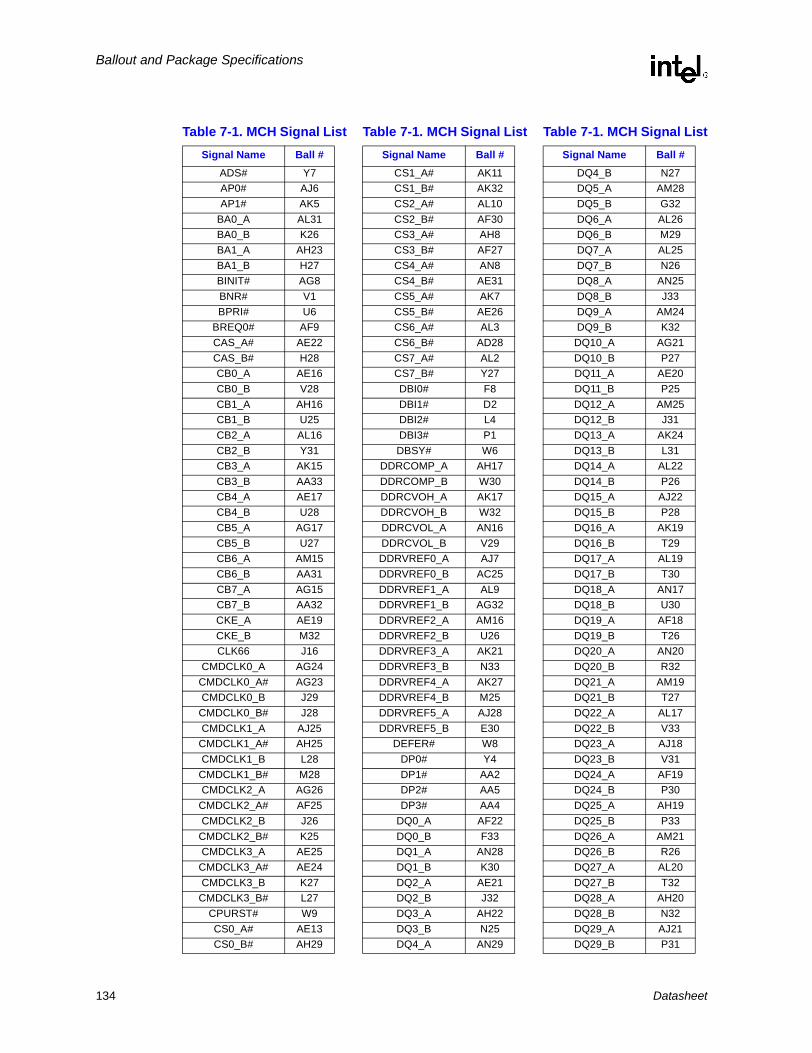
Ballout and Package Specifications
Table 7-1. MCH Signal ListSignal Name Ball #
ADS# Y7AP0# AJ6AP1# AK5
BA0_A AL31BA0_B K26BA1_A AH23BA1_B H27BINIT# AG8BNR# V1BPRI# U6
BREQ0# AF9CAS_A# AE22CAS_B# H28CB0_A AE16CB0_B V28CB1_A AH16CB1_B U25CB2_A AL16CB2_B Y31CB3_A AK15CB3_B AA33CB4_A AE17CB4_B U28CB5_A AG17CB5_B U27CB6_A AM15CB6_B AA31CB7_A AG15CB7_B AA32CKE_A AE19CKE_B M32CLK66 J16
CMDCLK0_A AG24CMDCLK0_A# AG23CMDCLK0_B J29
CMDCLK0_B# J28CMDCLK1_A AJ25
CMDCLK1_A# AH25CMDCLK1_B L28
CMDCLK1_B# M28CMDCLK2_A AG26
CMDCLK2_A# AF25CMDCLK2_B J26
CMDCLK2_B# K25CMDCLK3_A AE25
CMDCLK3_A# AE24CMDCLK3_B K27
CMDCLK3_B# L27CPURST# W9CS0_A# AE13CS0_B# AH29
CS1_A# AK11CS1_B# AK32CS2_A# AL10CS2_B# AF30CS3_A# AH8CS3_B# AF27CS4_A# AN8CS4_B# AE31CS5_A# AK7CS5_B# AE26CS6_A# AL3CS6_B# AD28CS7_A# AL2CS7_B# Y27DBI0# F8DBI1# D2DBI2# L4DBI3# P1DBSY# W6
DDRCOMP_A AH17DDRCOMP_B W30DDRCVOH_A AK17DDRCVOH_B W32DDRCVOL_A AN16DDRCVOL_B V29DDRVREF0_A AJ7DDRVREF0_B AC25DDRVREF1_A AL9DDRVREF1_B AG32DDRVREF2_A AM16DDRVREF2_B U26DDRVREF3_A AK21DDRVREF3_B N33DDRVREF4_A AK27DDRVREF4_B M25DDRVREF5_A AJ28DDRVREF5_B E30
DEFER# W8DP0# Y4DP1# AA2DP2# AA5DP3# AA4
DQ0_A AF22DQ0_B F33DQ1_A AN28DQ1_B K30DQ2_A AE21DQ2_B J32DQ3_A AH22DQ3_B N25DQ4_A AN29
Table 7-1. MCH Signal ListSignal Name Ball #
DQ4_B N27DQ5_A AM28DQ5_B G32DQ6_A AL26DQ6_B M29DQ7_A AL25DQ7_B N26DQ8_A AN25DQ8_B J33DQ9_A AM24DQ9_B K32DQ10_A AG21DQ10_B P27DQ11_A AE20DQ11_B P25DQ12_A AM25DQ12_B J31DQ13_A AK24DQ13_B L31DQ14_A AL22DQ14_B P26DQ15_A AJ22DQ15_B P28DQ16_A AK19DQ16_B T29DQ17_A AL19DQ17_B T30DQ18_A AN17DQ18_B U30DQ19_A AF18DQ19_B T26DQ20_A AN20DQ20_B R32DQ21_A AM19DQ21_B T27DQ22_A AL17DQ22_B V33DQ23_A AJ18DQ23_B V31DQ24_A AF19DQ24_B P30DQ25_A AH19DQ25_B P33DQ26_A AM21DQ26_B R26DQ27_A AL20DQ27_B T32DQ28_A AH20DQ28_B N32DQ29_A AJ21DQ29_B P31
Table 7-1. MCH Signal ListSignal Name Ball #
134 Datasheet

Ballout and Package Specifications
DQ30_A AN21DQ30_B R28DQ31_A AJ19DQ31_B T25DQ32_A AL14DQ32_B W27DQ33_A AM13DQ33_B AE33DQ34_A AJ15DQ34_B AF31DQ35_A AF15DQ35_B W25DQ36_A AK14DQ36_B AA28DQ37_A AN13DQ37_B AD32DQ38_A AH14DQ38_B AG33DQ39_A AG14DQ39_B W26DQ40_A AE14DQ40_B AA29DQ41_A AH13DQ41_B AB33DQ42_A AN12DQ42_B V26DQ43_A AL11DQ43_B AD31DQ44_A AE15DQ44_B Y28DQ45_A AF13DQ45_B AB32DQ46_A AJ12DQ46_B AB29DQ47_A AM10DQ47_B V25DQ48_A AE12DQ48_B Y25DQ49_A AH11DQ49_B AB27DQ50_A AG11DQ50_B AH32DQ51_A AN5DQ51_B AH31DQ52_A AG12DQ52_B AC28DQ53_A AF12DQ53_B AA26DQ54_A AM9DQ54_B AG30DQ55_A AM6
Table 7-1. MCH Signal ListSignal Name Ball #
DQ55_B AH33DQ56_A AG10DQ56_B AJ30DQ57_A AJ9DQ57_B AG29DQ58_A AM3DQ58_B AB25DQ59_A AM2DQ59_B AA25DQ60_A AH10DQ60_B AL32DQ61_A AE11DQ61_B AJ31DQ62_A AL5DQ62_B AC27DQ63_A AM4DQ63_B AB26DQS0_A AM27DQS0_B L30DQS1_A AL23DQS1_B M31DQS2_A AG18DQS2_B U33DQS3_A AE18DQS3_B R29DQS4_A AL13DQS4_B AE32DQS5_A AM12DQS5_B AC31DQS6_A AL8DQS6_B AE28DQS7_A AL6DQS7_B AE27DQS8_A AJ16DQS8_B W29DQS9_A AF21DQS9_B H31DQS10_A AK23DQS10_B N29DQS11_A AK18DQS11_B U31DQS12_A AK20DQS12_B R31DQS13_A AJ13DQS13_B AC30DQS14_A AK12DQS14_B AB30DQS15_A AM7DQS15_B AD27DQS16_A AH9DQS16_B AF28
Table 7-1. MCH Signal ListSignal Name Ball #
DQS17_A AF16DQS17_B Y30
DRDY# Y3HA3# AA8HA4# AB1HA5# AC3HA6# AD2HA7# AB6HA8# AC4HA9# AD4HA10# AE5HA11# AE2HA12# AC6HA13# AB9HA14# AE6HA15# AE3HA16# AD5HA17# AB8HA18# AC7HA19# AC9HA20# AH2HA21# AH3HA22# AG2HA23# AF6HA24# AD8HA25# AF1HA26# AG4HA27# AJ4HA28# AE8HA29# AF3HA30# AF7HA31# AH5HA32# AG7HA33# AH6HA34# AJ1HA35# AG5
HADSTB0# AE1HADSTB1# AD7HAVREF0 AF4HAVREF1 AJ3HCCVREF Y6HCLKINN U3HCLKINP T2
HD0# B9HD1# A9HD2# A4HD3# B5HD4# E8HD5# B3HD6# A5HD7# C8
Table 7-1. MCH Signal ListSignal Name Ball #
Datasheet 135

Ballout and Package Specifications
HD8# A8HD9# C4
HD10# C7HD11# D7HD12# H7HD13# C2HD14# J8HD15# J7HD16# F7HD17# L7HD18# L6HD19# E6HD20# G6HD21# D6HD22# F5HD23# E4HD24# M8HD25# E1HD26# F4HD27# D3HD28# F2HD29# E3HD30# F1HD31# M7HD32# H4HD33# H3HD34# G2HD35# K3HD36# G3HD37# J1HD38# K2HD39# K1HD40# N6HD41# J5HD42# P9HD43# M4HD44# P7HD45# N7HD46# R7HD47# R8HD48# L3HD49# N4HD50# P4HD51# M2HD52# L2HD53# N2HD54# N3HD55# N1HD56# R2HD57# T6HD58# T3
Table 7-1. MCH Signal ListSignal Name Ball #
HD59# U7HD60# T9HD61# T5HD62# R5HD63# T8
HDSTBN0# B6HDSTBN1# K6HDSTBN2# J2HDSTBN3# R4HDSTBP0# B8HDSTBP1# H6HDSTBP2# J4HDSTBP3# P3HDVREF0 C5HDVREF1 N8HDVREF2 P6HDVREF3 T7HI_STBF C10HI_STBS D10
HI0_A E11HI0_B D16HI0_C D22HI0_D D28HI1_A B11HI1_B G16HI1_C B24HI1_D G25HI2_A G10HI2_B C17HI2_C G18HI2_D G26HI3_A F10HI3_B C16HI3_C C22HI3_D F26HI4_A D9HI4_B A17HI4_C E20HI4_D G24HI5_A E9HI5_B A16HI5_C F19HI5_D A27HI6_A J11HI6_B B14HI6_C D21HI6_D H24HI7_A H9HI7_B D15HI7_C E21HI7_D C26
Table 7-1. MCH Signal ListSignal Name Ball #
HI8_A J13HI8_B C14HI8_C D19HI8_D G22HI9_A J10HI9_B F13HI9_C A20HI9_D E24HI10_A F11HI10_B A13HI10_C B20HI10_D A25HI11_A G12HI11_B C13HI11_C C19HI11_D D24HI12_B D12HI12_C B18HI12_D A24HI13_B E12HI13_C C18HI13_D E23HI14_B C11HI14_C E18HI14_D F23HI15_B J14HI15_C F17HI15_D F22HI16_B H14HI16_C B21HI16_D H23HI17_B B17HI17_C C24HI17_D H25HI18_B E14HI18_C F20HI18_D F25HI20_B F14HI20_C H18HI20_D E27HI21_B G13HI21_C F16HI21_D H21
HIRCOMP_A H11HIRCOMP_B E15HIRCOMP_C C20HIRCOMP_D G21HISWNG_A H12HISWNG_B B15HISWNG_C H17HISWNG_D F24
Table 7-1. MCH Signal ListSignal Name Ball #
136 Datasheet

Ballout and Package Specifications
HIT# U1HITM# W5
HIVREF_A G9HIVREF_B D13HIVREF_C A21HIVREF_D J22HLOCK# V7HREQ0# AB2HREQ1# AA1HREQ2# AA7HREQ3# AB3HREQ4# Y9HTRDY# W3
HXRCOMP V4HXSWING V8HYRCOMP G5HYSWING K5
MA0_A AF24MA0_B M26MA1_A AK26MA1_B K29MA2_A AH26MA2_B H30MA3_A AJ27MA3_B G30MA4_A AG27MA4_B F32MA5_A AH28MA5_B G29MA6_A AL28MA6_B F31MA7_A AL29MA7_B E33MA8_A AK29MA8_B E31MA9_A AM30MA9_B F29
MA10_A AJ24MA10_B L25MA11_A AK30MA11_B C31MA12_A AM31MA12_B C32
PSTRBF_B G15PSTRBF_C C23PSTRBF_D D27PSTRBS_B H15PSTRBS_C B23PSTRBS_D D26
PUSTRBF_B A12PUSTRBF_C D18
Table 7-1. MCH Signal ListSignal Name Ball #
PUSTRBF_D B25PUSTRBS_B B12PUSTRBS_C E17PUSTRBS_D C25PWRGOOD A28
RAS_A# AN24RAS_B# V32
RCVENIN_A# AM22RCVENIN_B# N30
RCVENOUT_A# AG20RCVENOUT_B# R25
Reserved B30Reserved AM18Reserved K33Reserved D29
RS0# V2RS1# V5RS2# U4RSP# AK4
RSTIN# E28SMB_CLK J25
SMB_DATA B31VCC_CPU AC5VCC_CPU AG3VCC_CPU AJ5VCC_CPU AF5VCC_CPU AH1VCC_CPU K7VCC_CPU F3VCC_CPU P5VCC_CPU R3VCC_CPU W7VCC_CPU H5VCC_CPU L5VCC_CPU U5VCC_CPU Y5VCC_CPU AE7VCC_CPU K9VCC_CPU AD1VCC_CPU D1VCC_CPU H1VCC_CPU M1VCC_CPU T1VCC_CPU Y1VCC_CPU A6VCC_CPU E7VCC_CPU AA10VCC_CPU AB11VCC_CPU AC10VCC_CPU C3VCC_CPU D5
Table 7-1. MCH Signal ListSignal Name Ball #
VCC_CPU L10VCC_CPU M11VCC_CPU N10VCC_CPU P11VCC_CPU R10VCC_CPU T11VCC_CPU U10VCC_CPU V11VCC_CPU W10VCC_CPU Y11VCC1_2 L18VCC1_2 L20VCC1_2 L22VCC1_2 B28VCC1_2 H20VCC1_2 A10VCC1_2 A14VCC1_2 A18VCC1_2 A22VCC1_2 E10VCC1_2 E13VCC1_2 E16VCC1_2 E19VCC1_2 E22VCC1_2 K13VCC1_2 K15VCC1_2 K17VCC1_2 K19VCC1_2 K21VCC1_2 K23VCC1_2 P14VCC1_2 P18VCC1_2 R17VCC1_2 R19VCC1_2 T14VCC1_2 T16VCC1_2 T18VCC1_2 U17VCC1_2 U19VCC1_2 V16VCC1_2 V18VCC1_2 W15VCC1_2 W17VCC1_2 W19VCC1_2 A26VCC1_2 A30VCC1_2 R15VCC1_2 V14VCC1_2 E26VCC1_2 H19VCC1_2 K11
Table 7-1. MCH Signal ListSignal Name Ball #
Datasheet 137

Ballout and Package Specifications
VCC1_2 L12VCC1_2 L14VCC1_2 L16VCC2_5 R23VCC2_5 AN4VCC2_5 AN7VCC2_5 AA23VCC2_5 AC13VCC2_5 AC15VCC2_5 AC17VCC2_5 AC19VCC2_5 U23VCC2_5 W23VCC2_5 AB24VCC2_5 AD12VCC2_5 AD14VCC2_5 AD16VCC2_5 AD18VCC2_5 AD20VCC2_5 AD25VCC2_5 AD29VCC2_5 AD33VCC2_5 AE10VCC2_5 AE30VCC2_5 AF33VCC2_5 AJ11VCC2_5 AJ14VCC2_5 AJ17VCC2_5 AJ20VCC2_5 AJ23VCC2_5 AK33VCC2_5 AN10VCC2_5 AN14VCC2_5 AN18VCC2_5 AN22VCC2_5 AN26VCC2_5 H33VCC2_5 L29VCC2_5 M33VCC2_5 P24VCC2_5 P29VCC2_5 T24VCC2_5 T33VCC2_5 U29VCC2_5 V24VCC2_5 Y24VCC2_5 Y29VCC2_5 Y33VCC2_5 AA27VCC2_5 AG13VCC2_5 AG19
Table 7-1. MCH Signal ListSignal Name Ball #
VCC2_5 AG22VCC2_5 AK10VCC2_5 AK8VCC2_5 AL1VCC2_5 AL15VCC2_5 AL24VCC2_5 G27VCC2_5 AC21VCC2_5 AC23VCC2_5 L23VCC2_5 N23VCC2_5 AD22VCC2_5 AD24VCC2_5 AJ26VCC2_5 AJ29VCC2_5 AN30VCC2_5 D33VCC2_5 E29VCC2_5 H29VCC2_5 K24VCC2_5 M24VCC2_5 AF23VCC2_5 AG28VCC2_5 AM32VCC2_5 B32VCC2_5 L26VCC2_5 AB31VCC2_5 K31VCC2_5 T31
VCCA1_2 P20VCCA1_2 T20VCCA1_2 V20VCCA1_2 Y14VCCA1_2 Y16VCCA1_2 Y18VCCA1_2 Y20
VCCACPU1_2 U15VCCAHI1_2 P16
VSS AD11VSS AD13VSS AD15VSS AD17VSS AD19VSS AD21VSS AD23VSS AD26VSS AD30VSS AE29VSS AE9VSS AF10VSS AF11
Table 7-1. MCH Signal ListSignal Name Ball #
VSS AF14VSS AF17VSS AF20VSS AF26VSS AF29VSS AF32VSS AG16VSS AG25VSS AG31VSS AH12VSS AH15VSS AH18VSS AH21VSS AH24VSS AH27VSS AH30VSS AJ32VSS AJ33VSS AK13VSS AK16VSS AK22VSS AK25VSS AK28VSS AK31VSS AL12VSS AL18VSS AL21VSS AL27VSS AL30VSS AL33VSS AM11VSS AM14VSS AM17VSS AM20VSS AM23VSS AM26VSS AM29VSS AN11VSS AK9VSS AM8VSS AC8VSS G7VSS D30VSS AF8VSS AA9VSS J6VSS V3VSS F28VSS AG6VSS AH7VSS AH4
Table 7-1. MCH Signal ListSignal Name Ball #
138 Datasheet

Ballout and Package Specifications
VSS AN15VSS AN19VSS AN23VSS AN27VSS AN3VSS AN31VSS AN6VSS B10VSS B13VSS B16VSS B19VSS B22VSS B26VSS B29VSS B4VSS B7VSS C1VSS C12VSS C15VSS C21VSS C27VSS C30VSS C33VSS C6VSS C9VSS D11VSS D14VSS D17VSS D20VSS D23VSS D31VSS D8VSS E25VSS E32VSS F12VSS F15VSS F18VSS F21VSS F27VSS F30VSS F6VSS F9VSS G1VSS G11VSS G14VSS G17VSS G20VSS G23VSS G28VSS G31VSS G33
Table 7-1. MCH Signal ListSignal Name Ball #
VSS AL4VSS AJ2VSS AK3VSS AD6VSS AK6VSS AL7VSS AM5VSS AF2VSS AD3VSS AG1VSS AK1VSS U9VSS E2VSS H2VSS K4VSS J3VSS K8VSS L8VSS G4VSS M6VSS P2VSS M3VSS M9VSS P8VSS N9VSS U2VSS R6VSS T4VSS V6VSS W4VSS W2VSS Y2VSS AA3VSS AA6VSS Y8VSS J19VSS J20VSS G19VSS E5VSS J23VSS AB5VSS D4VSS AE4VSS AC2VSS AG9VSS L9VSS C28VSS B27VSS AB4VSS AB7VSS AD9
Table 7-1. MCH Signal ListSignal Name Ball #
VSS G8VSS H10VSS H13VSS H16VSS H22VSS H26VSS H32VSS H8VSS J12VSS J15VSS J18VSS J21VSS J24VSS J27VSS J30VSS J9VSS K12VSS K14VSS K16VSS K18VSS K20VSS K22VSS K28VSS L1VSS L24VSS L32VSS L33VSS M23VSS M27VSS M30VSS N5VSS N24VSS N28VSS N31VSS P15VSS P17VSS P19VSS P23VSS P32VSS R1VSS R14VSS R18VSS R20VSS R24VSS R27VSS R30VSS R33VSS R9VSS T15VSS T17VSS T19
Table 7-1. MCH Signal ListSignal Name Ball #
Datasheet 139
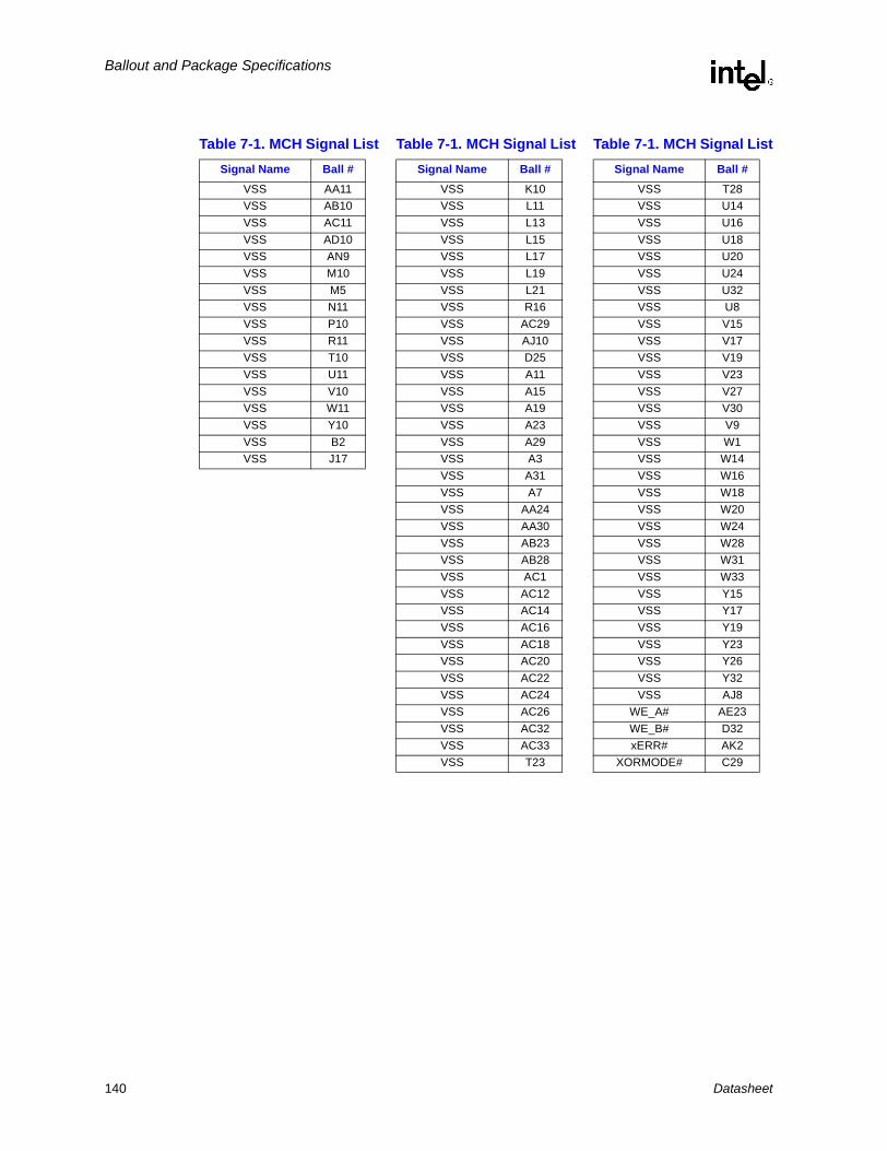
Ballout and Package Specifications
VSS AA11VSS AB10VSS AC11VSS AD10VSS AN9VSS M10VSS M5VSS N11VSS P10VSS R11VSS T10VSS U11VSS V10VSS W11VSS Y10VSS B2VSS J17
Table 7-1. MCH Signal ListSignal Name Ball #
VSS K10VSS L11VSS L13VSS L15VSS L17VSS L19VSS L21VSS R16VSS AC29VSS AJ10VSS D25VSS A11VSS A15VSS A19VSS A23VSS A29VSS A3VSS A31VSS A7VSS AA24VSS AA30VSS AB23VSS AB28VSS AC1VSS AC12VSS AC14VSS AC16VSS AC18VSS AC20VSS AC22VSS AC24VSS AC26VSS AC32VSS AC33VSS T23
Table 7-1. MCH Signal ListSignal Name Ball #
VSS T28VSS U14VSS U16VSS U18VSS U20VSS U24VSS U32VSS U8VSS V15VSS V17VSS V19VSS V23VSS V27VSS V30VSS V9VSS W1VSS W14VSS W16VSS W18VSS W20VSS W24VSS W28VSS W31VSS W33VSS Y15VSS Y17VSS Y19VSS Y23VSS Y26VSS Y32VSS AJ8
WE_A# AE23WE_B# D32xERR# AK2
XORMODE# C29
Table 7-1. MCH Signal ListSignal Name Ball #
140 Datasheet

Ballout and Package Specifications
7.2 Package SpecificationsFigure 7-4 and Figure 7-5 provide the package specifications for the MCH.
NOTE:1. All dimensions are in millimeters.2. All dimensions and tolerances conform to ANSI Y14.5M-1982.
Figure 7-4. MCH Package Dimensions (Top View)
AN
AM
AL
AK
AJ
AH
AG
AF
AE
AD
AC
AB
AA
Y
W
V
U
T
R
P
N
M
L
K
J
H
G
F
E
E
C
B
A
101620 3579111315194618 8121422 2124 2326
2528 2730 293132
(n)x 0.025 Min
Metal Edge(n)x ∅ 0.790 ± 0.025
Solder Resist Opening(n)x 0.650 ± 0.040Detail A
∅∅∅∅ 00.071 L C
∅∅∅∅ 00.200 L C A S B
33 12
1.270
20.320
40.640
2x 42.500 ±0.1000.200 A B
1.270
21.250
Detail A
17
Datasheet 141
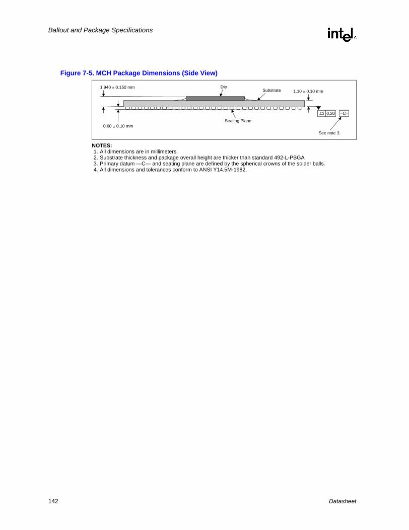
Ballout and Package Specifications
NOTES:1. All dimensions are in millimeters.2. Substrate thickness and package overall height are thicker than standard 492-L-PBGA3. Primary datum —C— and seating plane are defined by the spherical crowns of the solder balls.4. All dimensions and tolerances conform to ANSI Y14.5M-1982.
Figure 7-5. MCH Package Dimensions (Side View)
1.10 ± 0.10 mmDie
Substrate
0.60 ± 0.10 mmSeating Plane
1.940 ± 0.150 mm
0.20 –C–
See note 3.
142 Datasheet

Ballout and Package Specifications
7.3 Chipset Interface Trace Length CompensationIn this section, detailed information is given about the internal component package trace lengths to enable trace length compensation. Trace length compensation is required for platform design. These lengths must be considered when matching trace lengths as described in the Intel® Xeon™ Processor with 512-KB L2 Cache and Intel® E7500 Chipset Platform Design Guide. Note that these lengths represent the actual lengths from pad to ball.
The data given can be normalized from a particular reference ball to simplify routing. If the longest trace is used as the reference for normalization, use Equation 7-1.
Equation 7-1.
LREF is the nominal package length of the reference signal used for normalization.
∆LPKG is the nominal ∆ package trace length of the MCH from the reference trace.
To calculate the ∆LPCB for signals from the MCH to the device, use Equation 7-2.
Equation 7-2.
∆LPCB is the nominal ∆ PCB trace length to be added on the PCB.
∆LPKG is the nominal ∆ package trace length of the MCH (refer to Equation 1).
VPKG is the MCH package trace delay due to signal velocity. The nominal value is 150 ps/in.
VPCB is the PCB trace delay due to signal velocity. The nominal value is 175 ps/in on the recommended stackup.
Note: Use care when converting delays and velocities (x ps/in is a delay, y in/ps is a velocity).
Table 7-2 shows example values when signal MEMORY1 trace length is used for normalization.
PKGREFPKG LLL −=∆
PCB
PKGPKGPCB
VVLL ×∆=∆
Table 7-2. Example Normalization Table
LPKG (mils) ∆LPKG (mils) ∆LPCB (mils) Target LPCB (mils)
MEMORY1 175.984 0.000 0.000 3500.000
MEMORY2 152.364 23.620 20.246 3520.246
MEMORY3 130.315 45.669 39.145 3539.145
MEMORY4 118.897 57.087 48.932 3548.932
•••
•••
•••
•••
•••
MEMORYN 102.756 73.228 62.767 3562.767
Datasheet 143

Ballout and Package Specifications
7.3.1 MCH System Bus Signal Package Trace Length DataTable 7-3 is the MCH package trace length information for the system bus.
Table 7-3. MCH LPKG Data for the System Bus (Sheet 1 of 2)Signal Ball No. LPKG (mils) Signal Ball No. LPKG (mils)
HADSTB0# AE1 797.99 HDSTBN0# B6 842.99HA3# AA8 296.14 HDSTBP0# B8 739.72HA4# AB1 692.09 HD0# B9 682.48HA5# AC3 602.24 HD1# A9 775.98HA6# AD2 761.50 HD2# A4 955.20HA7# AB6 469.09 HD3# B5 933.07HA8# AC4 569.02 HD4# E8 648.77HA9# AD4 631.65 HD5# B3 1044.33HA10# AE5 612.17 HD6# A5 930.87HA11# AE2 781.97 HD7# C8 732.77HA12# AC6 469.44 HD8# A8 763.54HA13# AB9 578.15 HD9# C4 909.13HA14# AE6 576.69 HD10# C7 779.65HA15# AE3 702.60 HD11# D7 765.00HA16# AD5 512.91 HD12# H7 535.59
HREQ0# AB2 665.47 HD13# C2 1059.96HREQ1# AA1 684.80 HD14# J8 398.46HREQ2# AA7 397.91 HD15# J7 457.64HREQ3# AB3 591.46 DBI0# F8 596.13HREQ4# Y9 308.86
HDSTBN1# K6 480.24HADSTB1# AD7 430.11 HDSTBP1# H6 562.32
HA17# AB8 334.72 HD16# F7 617.72HA18# AC7 390.55 HD17# L7 378.98HA19# AC9 379.57 HD18# L6 450.04HA20# AH2 860.71 HD19# E6 762.64HA21# AH3 732.09 HD20# G6 680.20HA22# AG2 772.17 HD21# D6 771.73HA23# AF6 567.76 HD22# F5 809.84HA24# AD8 403.50 HD23# E4 859.72HA25# AF1 798.46 HD24# M8 334.68HA26# AG4 690.75 HD25# E1 1030.20HA27# AJ4 695.39 HD26# F4 851.54HA28# AE8 413.27 HD27# D3 892.64HA29# AF3 736.10 HD28# F2 945.08HA30# AF7 521.58 HD29# E3 905.20HA31# AH5 619.72 HD30# F1 1031.89HA32# AG7 497.28 HD31# M7 400.67HA33# AH6 601.73 DBI1# D2 981.89HA34# AJ1 877.87HA35# AG5 611.77
HCLKINN U3 639.53HCLKINP T2 639.61
144 Datasheet

Ballout and Package Specifications
7.3.1.1 MCH DDR Channel A Signal Package Trace Length Data
Table 7-4 is the MCH package trace length information for channel A of the DDR memory interface.
HDSTBN2# J2 783.19 HDSTBN3# R4 529.41HDSTBP2# J4 726.26 HDSTBP3# P3 605.71
HD32# H4 715.47 HD48# L3 669.41HD33# H3 803.03 HD49# N4 596.42HD34# G2 865.59 HD50# P4 584.80HD35# K3 723.94 HD51# M2 723.07HD36# G3 818.54 HD52# L2 729.17HD37# J1 803.50 HD53# N2 707.44HD38# K2 740.32 HD54# N3 605.91HD39# K1 821.65 HD55# N1 760.00HD40# N6 419.37 HD56# R2 613.43HD41# J5 720.87 HD57# T6 534.25HD42# P9 315.91 HD58# T3 580.20HD43# M4 622.60 HD59# U7 367.72HD44# P7 373.34 HD60# T9 271.46HD45# N7 351.31 HD61# T5 479.33HD46# R7 332.80 HD62# R5 451.46HD47# R8 306.89 HD63# T8 312.87DBI2# L4 649.69 DBI3# P1 686.77
Table 7-3. MCH LPKG Data for the System Bus (Sheet 2 of 2)Signal Ball No. LPKG (mils) Signal Ball No. LPKG (mils)
Table 7-4. MCH LPKG Data for DDR Channel A (Sheet 1 of 3)Signal Ball No. LPKG (mils) Signal Ball No. LPKG (mils)
DQS0_A AM27 760.59 DQS2_A AG18 338.67DQS9_A AF21 291.45 DQS11_A AK18 477.64DQ0_A AF22 345.91 DQ16_A AK19 499.02DQ1_A AN28 853.78 DQ17_A AL19 583.11DQ2_A AE21 284.59 DQ18_A AN17 674.17DQ3_A AH22 447.83 DQ19_A AF18 297.50DQ4_A AN29 867.36 DQ20_A AN20 697.09DQ5_A AM28 817.76 DQ21_A AM19 630.75DQ6_A AL26 707.24 DQ22_A AL17 534.80DQ7_A AL25 642.13 DQ23_A AJ18 455.77
DQS1_A AL23 602.87 DQS3_A AE18 226.03DQS10_A AK23 552.99 DQS12_A AK20 500.71
DQ8_A AN25 761.06 DQ24_A AF19 300.32DQ9_A AM24 712.95 DQ25_A AH19 423.19
DQ10_A AG21 371.89 DQ26_A AM21 625.04DQ11_A AE20 273.13 DQ27_A AL20 578.15DQ12_A AM25 737.68 DQ28_A AH20 440.20DQ13_A AK24 607.13 DQ29_A AJ21 503.66DQ14_A AL22 578.43 DQ30_A AN21 703.07DQ15_A AJ22 475.71 DQ31_A AJ19 438.58
Datasheet 145

Ballout and Package Specifications
DQS4_A AL13 595.67 DQS7_A AL6 733.15DQS13_A AJ13 473.62 DQS16_A AH9 483.27DQ32_A AL14 586.58 DQ56_A AG10 446.54DQ33_A AM13 662.60 DQ57_A AJ9 572.13DQ34_A AJ15 512.60 DQ58_A AM3 957.28DQ35_A AF15 350.43 DQ59_A AM2 990.51DQ36_A AK14 516.50 DQ60_A AH10 527.88DQ37_A AN13 730.83 DQ61_A AE11 337.46DQ38_A AH14 447.76 DQ62_A AL5 779.02DQ39_A AG14 358.19 DQ63_A AM4 882.36
DQS5_A AM12 693.27 DQS8_A AJ16 432.48DQS14_A AK12 531.46 DQS17_A AF16 281.57DQ40_A AE14 402.72 CB0_A AE16 256.61DQ41_A AH13 453.46 CB1_A AH16 412.22DQ42_A AN12 704.45 CB2_A AL16 559.57DQ43_A AL11 666.30 CB3_A AK15 560.08DQ44_A AE15 270.32 CB4_A AE17 375.28DQ45_A AF13 344.49 CB5_A AG17 359.80DQ46_A AJ12 506.22 CB6_A AM15 656.14DQ47_A AM10 703.35 CB7_A AG15 371.50
DQS6_A AL8 676.58DQS15_A AM7 755.79DQ48_A AE12 278.66DQ49_A AH11 463.74DQ50_A AG11 441.73DQ51_A AN5 898.50DQ52_A AG12 412.05DQ53_A AF12 377.68DQ54_A AM9 742.17DQ55_A AM6 855.47
Table 7-4. MCH LPKG Data for DDR Channel A (Sheet 2 of 3)Signal Ball No. LPKG (mils) Signal Ball No. LPKG (mils)
146 Datasheet

Ballout and Package Specifications
CMDCLK0_A AG24 447.35 CMDCLK2_A AG26 459.06CMDCLK0_A# AG23 405.28 CMDCLK2_A# AF25 367.24
BA0_A AL31 789.29 BA0_A AL31 789.29BA1_A AH23 427.72 BA1_A AH23 427.72
CAS_A# AE22 411.22 CAS_A# AE22 411.22CKE_A AE19 249.80 CKE_A AE19 249.80CS0_A# AE13 434.96 CS4_A# AN8 805.28CS1_A# AK11 594.41 CS5_A# AK7 716.34MA0_A AF24 340.16 MA0_A AF24 340.16MA1_A AK26 640.55 MA1_A AK26 640.55MA2_A AH26 512.01 MA2_A AH26 512.01MA3_A AJ27 568.58 MA3_A AJ27 568.58MA4_A AG27 466.97 MA4_A AG27 466.97MA5_A AH28 595.79 MA5_A AH28 595.79MA6_A AL28 791.89 MA6_A AL28 791.89MA7_A AL29 735.71 MA7_A AL29 735.71MA8_A AK29 698.35 MA8_A AK29 698.35MA9_A AM30 827.80 MA9_A AM30 827.80
MA10_A AJ24 572.17 MA10_A AJ24 572.17MA11_A AK30 712.64 MA11_A AK30 712.64MA12_A AM31 865.00 MA12_A AM31 865.00RAS_A# AN24 757.84 RAS_A# AN24 757.84WE_A# AE23 298.19 WE_A# AE23 298.19
CMDCLK1_A AJ25 544.88 CMDCLK3_A AE25 359.80CMDCLK1_A# AH25 473.52 CMDCLK3_A# AE24 322.68
BA0_A AL31 789.29 BA0_A AL31 789.29BA1_A AH23 427.72 BA1_A AH23 427.72
CAS_A# AE22 411.22 CAS_A# AE22 411.22CKE_A AE19 249.80 CKE_A AE19 249.80CS2_A# AL10 641.10 CS6_A# AL3 892.80CS3_A# AH8 622.17 CS7_A# AL2 917.36MA0_A AF24 340.16 MA0_A AF24 340.16MA1_A AK26 640.55 MA1_A AK26 640.55MA2_A AH26 512.01 MA2_A AH26 512.01MA3_A AJ27 568.58 MA3_A AJ27 568.58MA4_A AG27 466.97 MA4_A AG27 466.97MA5_A AH28 595.79 MA5_A AH28 595.79MA6_A AL28 791.89 MA6_A AL28 791.89MA7_A AL29 735.71 MA7_A AL29 735.71MA8_A AK29 698.35 MA8_A AK29 698.35MA9_A AM30 827.80 MA9_A AM30 827.80
MA10_A AJ24 572.17 MA10_A AJ24 572.17MA11_A AK30 712.64 MA11_A AK30 712.64MA12_A AM31 865.00 MA12_A AM31 865.00RAS_A# AN24 757.84 RAS_A# AN24 757.84WE_A# AE23 298.19 WE_A# AE23 298.19
Table 7-4. MCH LPKG Data for DDR Channel A (Sheet 3 of 3)Signal Ball No. LPKG (mils) Signal Ball No. LPKG (mils)
Datasheet 147

Ballout and Package Specifications
7.3.1.2 MCH DDR Channel B Signal Package Trace Length Data
Table 7-5 is the MCH package trace length information for channel B of the DDR memory interface.
f
Table 7-5. MCH LPKG Data for DDR Channel B (Sheet 1 of 3)Signal Ball No. LPKG (mils) Signal Ball No. LPKG (mils)
DQS0_B L30 545.94 DQS3_B R29 445.98DQS9_B H31 698.39 DQS12_B R31 541.50DQ0_B F33 870.43 DQ24_B P30 523.82DQ1_B K30 639.33 DQ25_B P33 694.80DQ2_B J32 695.67 DQ26_B R26 287.40DQ3_B N25 275.85 DQ27_B T32 586.46DQ4_B N27 344.82 DQ28_B N32 655.83DQ5_B G32 796.61 DQ29_B P31 587.64DQ6_B M29 488.98 DQ30_B R28 415.72DQ7_B N26 329.65 DQ31_B T25 307.72
DQS1_B M31 586.65 DQS4_B AE32 756.46DQS10_B N29 459.05 DQS13_B AC30 609.57
DQ8_B J33 765.35 DQ32_B W27 375.75DQ9_B K32 724.84 DQ33_B AE33 825.12
DQ10_B P27 361.38 DQ34_B AF31 780.55DQ11_B P25 246.21 DQ35_B W25 627.56DQ12_B J31 710.35 DQ36_B AA28 499.10DQ13_B L31 635.83 DQ37_B AD32 766.85DQ14_B P26 322.21 DQ38_B AG33 863.70DQ15_B P28 423.86 DQ39_B W26 328.87
DQS2_B U33 660.43 DQS5_B AC31 692.56DQS11_B U31 545.16 DQS14_B AB30 598.03DQ16_B T29 441.22 DQ40_B AA29 567.36DQ17_B T30 511.14 DQ41_B AB33 769.02DQ18_B U30 523.03 DQ42_B V26 288.03DQ19_B T26 318.23 DQ43_B AD31 746.26DQ20_B R32 631.77 DQ44_B Y28 421.18DQ21_B T27 366.58 DQ45_B AB32 743.46DQ22_B V33 697.36 DQ46_B AB29 590.71DQ23_B V31 556.89 DQ47_B V25 633.50
148 Datasheet

Ballout and Package Specifications
DQS6_B AE28 569.17 DQS8_B W29 470.79DQS15_B AD27 502.05 DQS17_B Y30 551.26DQ48_B Y25 247.68 CB0_B V28 422.40DQ49_B AB27 417.01 CB1_B U25 262.04DQ50_B AH32 865.47 CB2_B Y31 639.37DQ51_B AH31 860.08 CB3_B AA33 724.06DQ52_B AC28 547.40 CB4_B U28 421.42DQ53_B AA26 339.80 CB5_B U27 356.31DQ54_B AG30 780.12 CB6_B AA31 605.00DQ55_B AH33 946.54 CB7_B AA32 701.69
DQS7_B AE27 488.39DQS16_B AF28 548.74DQ56_B AJ30 741.93DQ57_B AG29 692.99DQ58_B AB25 480.35DQ59_B AA25 260.73DQ60_B AL32 924.06DQ61_B AJ31 816.65DQ62_B AC27 478.39DQ63_B AB26 360.59
Table 7-5. MCH LPKG Data for DDR Channel B (Sheet 2 of 3)Signal Ball No. LPKG (mils) Signal Ball No. LPKG (mils)
Datasheet 149

Ballout and Package Specifications
CMDCLK0_B J29 595.43 CMDCLK2_B J26 397.24CMDCLK0_B# J28 539.65 CMDCLK2_B# K25 313.50
BA0_B K26 370.75 BA0_B K26 370.75BA1_B H27 430.16 BA1_B H27 430.16
CAS_B# H28 542.21 CAS_B# H28 542.21CKE_B M32 660.59 CKE_B M32 660.59CS0_B# AH29 693.82 CS4_B# AE31 739.72CS1_B# AK32 899.92 CS5_B# AE26 463.94MA0_B M26 333.74 MA0_B M26 333.74MA1_B K29 540.43 MA1_B K29 540.43MA2_B H30 659.69 MA2_B H30 659.69MA3_B G30 705.39 MA3_B G30 705.39MA4_B F32 793.19 MA4_B F32 793.19MA5_B G29 612.68 MA5_B G29 612.68MA6_B F31 747.72 MA6_B F31 747.72MA7_B E33 892.05 MA7_B E33 892.05MA8_B E31 728.54 MA8_B E31 728.54MA9_B F29 603.94 MA9_B F29 603.94
MA10_B L25 435.71 MA10_B L25 435.71MA11_B C31 794.25 MA11_B C31 794.25MA12_B C32 813.07 MA12_B C32 813.07RAS_B# V32 651.06 RAS_B# V32 651.06WE_B# D32 818.43 WE_B# D32 818.43
CMDCLK1_B L28 417.28 CMDCLK3_B K27 423.70CMDCLK1_B# M28 405.28 CMDCLK3_B# L27 400.43
BA0_B K26 370.75 BA0_B K26 370.75BA1_B H27 430.16 BA1_B H27 430.16
CAS_B# H28 542.21 CAS_B# H28 542.21CKE_B M32 660.59 CKE_B M32 660.59CS2_B# AF30 739.06 CS6_B# AD28 575.79CS3_B# AF27 515.04 CS7_B# Y27 353.35MA0_B M26 333.74 MA0_B M26 333.74MA1_B K29 540.43 MA1_B K29 540.43MA2_B H30 659.69 MA2_B H30 659.69MA3_B G30 705.39 MA3_B G30 705.39MA4_B F32 793.19 MA4_B F32 793.19MA5_B G29 612.68 MA5_B G29 612.68MA6_B F31 747.72 MA6_B F31 747.72MA7_B E33 892.05 MA7_B E33 892.05MA8_B E31 728.54 MA8_B E31 728.54MA9_B F29 603.94 MA9_B F29 603.94
MA10_B L25 435.71 MA10_B L25 435.71MA11_B C31 794.25 MA11_B C31 794.25MA12_B C32 813.07 MA12_B C32 813.07RAS_B# V32 651.06 RAS_B# V32 651.06WE_B# D32 818.43 WE_B# D32 818.43
Table 7-5. MCH LPKG Data for DDR Channel B (Sheet 3 of 3)Signal Ball No. LPKG (mils) Signal Ball No. LPKG (mils)
150 Datasheet

Ballout and Package Specifications
7.3.1.3 MCH Hub Interface_A Signal Package Trace Length Data
Table 7-6 is the MCH package trace length information for Hub Interface_A.
7.3.1.4 MCH Hub Interface_B Signal Package Trace Length Data
Table 7-7 is the MCH package trace length information for Hub Interface_B.
Table 7-6. MCH LPKG Data for Hub Interface_A
Signal Ball No. LPKG (mils)
HI_STBF C10 659.09HI_STBS D10 623.43
HI0_A E11 519.92HI1_A B11 743.78HI2_A G10 468.03HI3_A F10 501.54HI4_A D9 633.62HI5_A E9 543.11HI6_A J11 317.83HI7_A H9 426.55
Table 7-7. MCH LPKG Data for Hub Interface_BSignal Ball No. LPKG (mils) Signal Ball No. LPKG (mils)
PSTRBF_B G15 333.78 PUSTRBF_B A12 678.70PSTRBS_B H15 300.32 PUSTRBS_B B12 645.75
HI0_B D16 482.83 HI8_B C14 591.54HI1_B G16 478.27 HI9_B F13 433.19HI2_B C17 544.45 HI10_B A13 702.76HI3_B C16 571.54 HI11_B C13 568.78HI4_B A17 677.56 HI12_B D12 518.46HI5_B A16 679.33 HI13_B E12 504.53HI6_B B14 597.40 HI14_B C11 611.77HI7_B D15 531.18 HI15_B J14 272.14HI20_B F14 414.53 HI21_B G13 386.58
Datasheet 151

Ballout and Package Specifications
7.3.1.5 MCH Hub Interface_C Signal Package Trace Length Data
Table 7-8 is the MCH package trace length information for Hub Interface_C.
7.3.1.6 MCH Hub Interface_D Signal Package Trace Length Data
Table 7-9 is the MCH package trace length information for Hub Interface_D.
Table 7-8. MCH LPKG Data for Hub Interface_C
Signal Ball No. LPKG (mils) Signal Ball No. LPKG (mils)
PSTRBF_C C23 681.10 PUSTRBF_C D18 514.80PSTRBS_C B23 732.52 PUSTRBS_C E17 464.80
HI0_C D22 635.32 HI8_C D19 557.40HI1_C B24 757.96 HI9_C A20 728.98HI2_C G18 360.95 HI10_C B20 665.71HI3_C C22 696.42 HI11_C C19 616.69HI4_C E20 495.43 HI12_C B18 650.47HI5_C F19 394.84 HI13_C C18 561.77HI6_C D21 609.57 HI14_C E18 453.94HI7_C E21 516.69 HI15_C F17 379.61
HI20_C H18 294.76 HI21_C F16 416.61
Table 7-9. MCH LPKG Data for Hub Interface_DSignal Ball No. LPKG (mils) Signal Ball No. LPKG (mils)
PSTRBF_D D27 720.08 PUSTRBF_D B25 760.04PSTRBS_D D26 731.54 PUSTRBS_D C25 716.14
HI0_D D28 772.84 HI8_D G22 496.18HI1_D G25 565.51 HI9_D E24 588.62HI2_D G26 538.23 HI10_D A25 816.22HI3_D F26 592.94 HI11_D D24 618.90HI4_D G24 517.40 HI12_D A24 808.66HI5_D A27 902.48 HI13_D E23 526.58HI6_D H24 416.58 HI14_D F23 494.53HI7_D C26 745.28 HI15_D F22 497.05HI20_D E27 700.00 HI21_D H21 502.40
152 Datasheet

Testability
Testability 8
In the MCH, the ability for Automated Test Equipment (ATE) board-level testing has been implemented as an XOR chain. An XOR chain is a chain of XOR gates, each with one input pin connected to it.
The MCH uses the XORMODE# pin to activate the XOR test mode. The method to put the MCH in XOR test is to assert the XORMODE# signal. When the following conditions are met, the chip will be in XOR test mode. If any of the following are not met, then XOR test will not be enabled.
1. Assert PWRGOOD
2. Assert RSTIN# for 128 clocks beyond the assertion of PWRGOOD (RSTIN# may be held asserted before PWRGOOD is asserted).
3. Deassert RSTIN#
4. Assert XORMODE# and hold asserted.
5. The clocks may be held at the 0 or 1 state; or be fully running. Since HCLKINP/HCLKINN is a differential pair, the 2 clock inputs should be held in opposite states.
6. As long as XORMODE# is asserted the MCH is in XOR test. As soon as XORMODE# is asserted and 2 HCLKINP/HCLKINN cycles have occurred, all the XOR chains are functional.
7. After deasserting XORMODE#, the MCH should be reset before any other testing is done.
There are eight chains of XORs divided up functionally.
Note: For all test modes except Asynchronous XOR mode, input pin XORMODE# should be driven high.
Datasheet 153
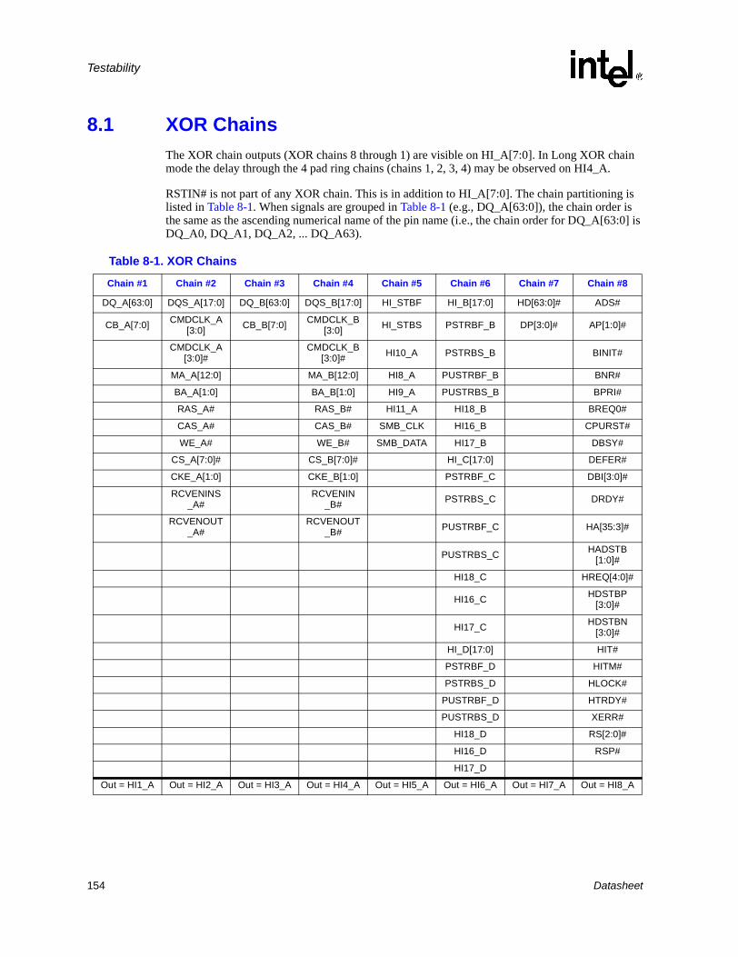
Testability
8.1 XOR ChainsThe XOR chain outputs (XOR chains 8 through 1) are visible on HI_A[7:0]. In Long XOR chain mode the delay through the 4 pad ring chains (chains 1, 2, 3, 4) may be observed on HI4_A.
RSTIN# is not part of any XOR chain. This is in addition to HI_A[7:0]. The chain partitioning is listed in Table 8-1. When signals are grouped in Table 8-1 (e.g., DQ_A[63:0]), the chain order is the same as the ascending numerical name of the pin name (i.e., the chain order for DQ_A[63:0] is DQ_A0, DQ_A1, DQ_A2, ... DQ_A63).
Table 8-1. XOR Chains
Chain #1 Chain #2 Chain #3 Chain #4 Chain #5 Chain #6 Chain #7 Chain #8
DQ_A[63:0] DQS_A[17:0] DQ_B[63:0] DQS_B[17:0] HI_STBF HI_B[17:0] HD[63:0]# ADS#
CB_A[7:0] CMDCLK_A[3:0] CB_B[7:0] CMDCLK_B
[3:0] HI_STBS PSTRBF_B DP[3:0]# AP[1:0]#
CMDCLK_A[3:0]#
CMDCLK_B[3:0]# HI10_A PSTRBS_B BINIT#
MA_A[12:0] MA_B[12:0] HI8_A PUSTRBF_B BNR#
BA_A[1:0] BA_B[1:0] HI9_A PUSTRBS_B BPRI#
RAS_A# RAS_B# HI11_A HI18_B BREQ0#
CAS_A# CAS_B# SMB_CLK HI16_B CPURST#
WE_A# WE_B# SMB_DATA HI17_B DBSY#
CS_A[7:0]# CS_B[7:0]# HI_C[17:0] DEFER#
CKE_A[1:0] CKE_B[1:0] PSTRBF_C DBI[3:0]#
RCVENINS_A#
RCVENIN_B# PSTRBS_C DRDY#
RCVENOUT_A#
RCVENOUT_B# PUSTRBF_C HA[35:3]#
PUSTRBS_C HADSTB[1:0]#
HI18_C HREQ[4:0]#
HI16_C HDSTBP[3:0]#
HI17_C HDSTBN[3:0]#
HI_D[17:0] HIT#
PSTRBF_D HITM#
PSTRBS_D HLOCK#
PUSTRBF_D HTRDY#
PUSTRBS_D XERR#
HI18_D RS[2:0]#
HI16_D RSP#
HI17_D
Out = HI1_A Out = HI2_A Out = HI3_A Out = HI4_A Out = HI5_A Out = HI6_A Out = HI7_A Out = HI8_A
154 Datasheet