Embed Size (px)
Citation preview

Integrated silicon carbide modulator for CMOS 1
photonics 2 3
Keith Powell1,2, Liwei Li1, Amirhassan Shams-Ansari2, Jianfu Wang1, Debin Meng1, Neil Sinclair2,3, Jiangdong Deng4, 4 Marko Lončar2* & Xiaoke Yi1* 5 6 Author affiliations. 1School of Electrical and Information Engineering, the University of Sydney, NSW 2006, Australia. 7 2John A. Paulson School of Engineering and Applied Sciences, Harvard University, Cambridge, MA 02138, USA. 3Division 8 of Physics, Mathematics and Astronomy, and Alliance for Quantum Technologies (AQT), California Institute of 9 Technology, 1200 E. California Boulevard, Pasadena, CA 91125, USA. 4Center for Nanoscale Systems, Harvard University, 10 Cambridge, MA 02138, USA. 11 *E-mail: [email protected]; [email protected] 12 13
14 The electro-optic modulator encodes electrical signals onto an optical carrier, and is essential 15
for the operation of global communication systems and data centers that society demands1. An 16
ideal modulator results from scalable semiconductor fabrication and is integratable with 17
electronics. Accordingly, it is compatible with complimentary metal-oxide semiconductor (CMOS) 18
fabrication processes. Moreover, modulators using the Pockels effect enables low loss, ultrafast and 19
wide-bandwidth data transmission. Although strained silicon-based modulators could satisfy these 20
criteria, fundamental limitations such as two-photon absorption, poor thermal stability and a 21
narrow transparency window hinder their performance. On the other hand, as a wide bandgap 22
semiconductor matrial, silicon carbide is CMOS compatible and does not suffer from these 23
limitations. Due to its combination of color centers, high breakdown voltage, and strong thermal 24
conductivity, silicon carbide is a promising material for CMOS electronics and photonics with 25
applications ranging from sensors to quantum and nonlinear photonics2-4. Importantly, silicon 26
carbide exhibits the Pockels effect, but a modulator has not been realized since the discovery of this 27
effect more than three decades ago. Here we design, fabricate, and demonstrate the first Pockels 28
modulator in silicon carbide. Specifically, we realize a waveguide-integrated, small form-factor, 29
gigahertz-bandwidth modulator that can operate using CMOS-level drive voltages on a thin film 30
of silicon carbide on insulator. Furthermore, the device features no signal degredation and stable 31
operation at high optical intensities (913 kW/mm2), allowing for high optical signal-to-noise ratios 32

for long distance communications. Our work unites Pockels electro-optics with a CMOS platform 33
to pave the way for foundry-compatible integrated photonics. 34
The convergence of photonics and CMOS electronics empowers photonic integrated circuits to meet 35
the ever-increasing demand for data throughput in information systems5,6. In particular, the electro-optic 36
(EO) modulator is at the center of this convergence as a critical component for encoding electrical signals 37
onto light for applications in datacenters, telecommunication networks and microwave photonic systems. 38
State-of-the-art modulators based on silicon, the workhorse material of electronics, rely on the free carrier 39
plasma dispersion effect. This effect is intrinsically absorptive and nonlinear as it causes coupled phase 40
and amplitude modulation, which distorts the signal modulation amplitude and restrict usage of advanced 41
modulation formats7. Alternatively, EO modulators based on the Pockels effect i.e. linear EO effect, 42
which exists in non-centrosymmetric crystals, allows the refractive index to vary linearly and rapidly in 43
proportion to an applied electric field. Consequently, Pockels modulators are exploited to achieve high 44
data rates and conversion efficiencies without the addition of optical loss8. The Pockels effect is not 45
present in most materials in the CMOS family, including silicon and silicon nitride. Aluminum nitride 46
(AlN) exhibits the Pockels effect with non-equal EO tensors, and has relatively low refractive index, 47
which increases the complexity in dense optoelectronic integration9. Modifications to the crystal 48
symmetry of CMOS materials by strain have been proposed to realize EO modulators10-12, but suffer from 49
trade-offs fabrication complexity. For example, strained silicon11,12 suffers from two-photon optical 50
absorption and poor thermal stability that is inherent to silicon. Furthermore, the relatively small indirect 51
bandgap of silicon prevents the usage of silicon waveguide in the visible spectrum range, which is of 52
great interest for applications in sensing and quantum optics13,14. Commonly-used lithium niobate 53
(LiNbO3) Pockels modulators have a strong EO coefficient15. However, they suffer from signal-distortion 54
induced by photorefraction that worsens with increasing optical powers16, and is avoided by post-55
modulation amplification in applications. Moreover, low costs and high yields on chip are required, as 56
permitted by the integration via CMOS compatible fabrication17. 57
One CMOS-compatible material that exhibits the Pockels effect is silicon carbide (SiC)18. In 58
particular, the cubic (3C) polytype of SiC has the largest measured EO coefficient (~ 2.7 pm/V at 633 59
nm) of all SiC polytypes and has equal elements of the EO tensor19, which simplifies optoelectronic 60
integration. Moreover, the wide bandgap of SiC allows broadband optical transparency from ultraviolet 61
to infrared. Despite this, a SiC-based Pockels modulator has not been experimentally demonstrated due 62
to poor crystal quality and difficulty obtaining low-loss waveguides20–23. Although 3C-SiC can be grown 63
directly onto a silicon substrate, it has been difficult to realize high-quality thin films, due to crystal 64
defects associated with this approach23,24. Wafer bonding techniques25 and annealing processes26 have 65
been explored to address these problems. Yet, the former demonstrates multimode waveguides while the 66
latter still results in a high (7 dB/cm) optical loss. These issues undermine a 3C-SiC Pockels modulator, 67
specifically one that features single-mode waveguides for stable and high extinction-ratio ring modulators 68
or quantum applications27. 69
Moreover, due to its high electron mobility, as well as robust properties27-30, SiC is a compelling 70
semiconductor material for next-generation CMOS electronics and a contender for realizing monolithic 71
integration of quantum and nonlinear photonics2,3,27,31,32. By taking the advantage of its high thermal 72
conductivity33, wide band-gap, low thermo-optic coefficient26 and high refractive index (~2.57)34, SiC 73
offers the possibility of densely integrated and robust photonic devices with low fabrication costs via 74
CMOS-compatible nanofabrication35 and the potential for integration with electronics. 75
Here we present the first SiC EO modulator. Optical modulation is achieved by electrically driving a 76
microring resonator in sub-micron-wide 3C-SiC on insulator waveguides via the Pockels effect. A 77
microring is chosen to enable a compact device footprint (90 µm2), while maintaining high modulation 78
performance at low voltage. The modulator is fabricated with a CMOS-compatible process and operates 79
at a transmission rate of up to 15 gigabits per second using CMOS-level drive voltages. Importantly, we 80
reduce the impact of polycrystal grains and waveguide surface roughness to demonstrate ~5.4 dB/cm 81
optical loss using a single-mode waveguide. As a result of our work, we measure the Pockels coefficient 82

(1.5 pm/V) of 3C-SiC at an infrared wavelength for the first time. Moreover, the modulator is able to 83
operate continuously with high optical intensities of up to 913 kW/mm2 without signal degradation, 84
facilitating low-noise microwave photonics36 or parametric conversion of single photons37. 85
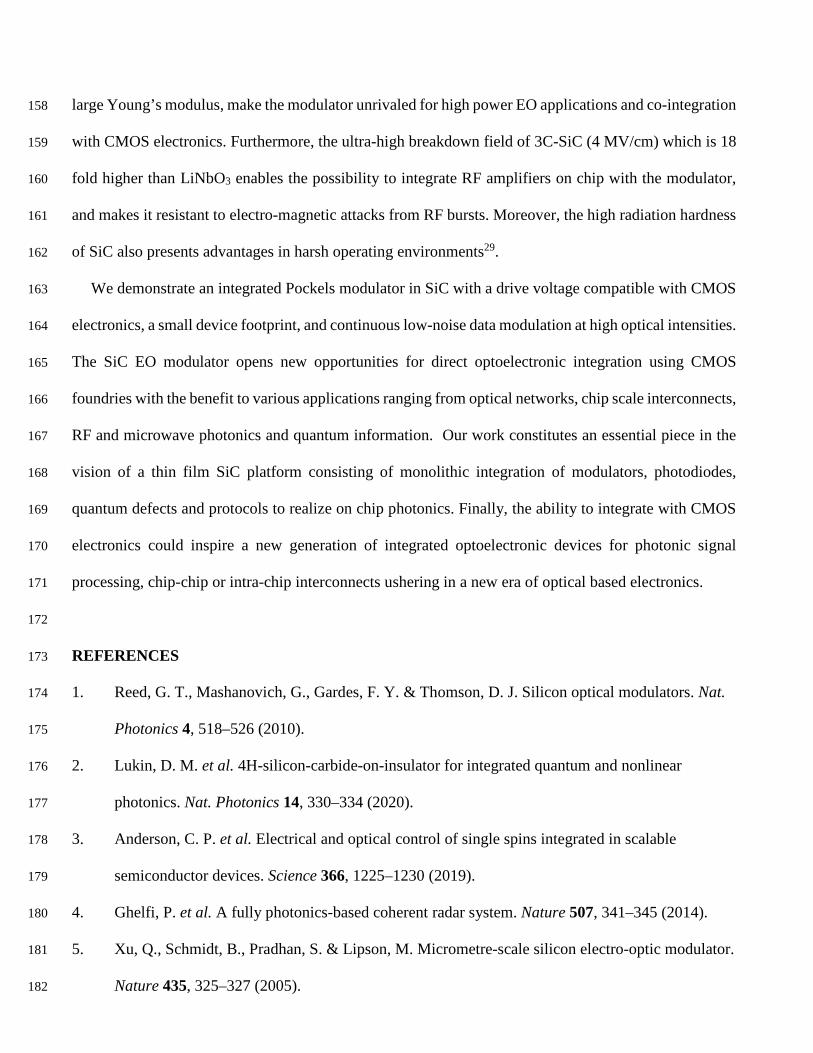
The fabrication of the integrated 3C-SiC modulator begins with the 530 nm-thick SiC layer with a low 86
crystal defect density (see Methods) to reduce the scattering or absorption losses and increase EO 87
interaction. Figure 1a shows an optical micrograph of a fabricated modulator capable of operating using 88
a CMOS digital to analog converter (DAC). The modulator consists of a pair of 3C-SiC vertical grating 89
couplers (VGCs) as optical input and output ports, an optical waveguide ring resonator with a loaded 90
quality (QL) factor of 34,310 to balance modulation efficiency and bandwidth38, and microwave strip line 91
electrodes to deliver electrical signals. The waveguides and the VGCs are structured by electron beam 92
lithography (EBL) (see Methods), in which a typical waveguide width of 800 nm is chosen to maintain 93
single mode operation with high optical mode confinement. The electrodes consist of a pair of ground 94
electrodes placed next to the sides of the waveguide and a signal electrode above the waveguide (Fig.1b). 95
A 1-μm-thick top cladding SiO2 layer is deposited to separate the electrode to the waveguide, which 96
prevents optical loss from mode interaction with the metal. Figure 1c shows a cross sectional scanning 97
electron micrograph (SEM) of the modulator to illustrate the geometries of the waveguide and electrodes. 98
The electrode thickness (~500 nm) is chosen to reduce radio frequency (RF) loss due to the skin effect. 99
As depicted in Fig. 1d, when a voltage is applied across the signal and ground electrodes, a vertical 100
electric field is induced predominantly in the vertical direction overlapping with the optical mode to probe 101
the Pockels effect. The ring cavity enables the phase change to be translated into an intensity modulated 102
output, where the resonant enhancement of the modulator allows for a small device footprint and low 103
drive voltage operation. Figure 1e shows a SEM of our etched waveguide, which can achieve a root-104
mean-squared sidewall roughness less than 2.4 nm26 facilitating absorption limited optical loss. To 105
qualify the optical loss, the optical spectrum of the microring resonator with critically coupled resonances 106
operating at the telecommunication wavelengths (1569 nm - 1600 nm) is measured to reveal single mode 107

operation (Fig. 1f) with a resonance linewidth of 36.9 pm (Fig. 1g). The obtained intrinsic Q (QI) is 108
86,000 corresponding to a linear propagation loss of ~5.4 dB/cm. 109
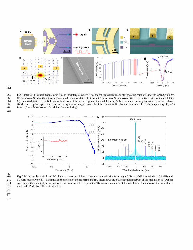
To characterize the maximum operational bandwidth of our fabricated modulator, we examine the EO 110
response at an optical input power of 6.8 mW (see Methods), which shows a 3 dB bandwidth of 7.1 GHz 111
(Fig. 2a). The bandwidth is limited by the cavity photon lifetime of 28 ps, calculated based on the 112
measured cavity linewidth (45 pm), that corresponds to the modulation bandwidth of around 5.7 GHz. 113
The electrode circuit of the modulator has much broader spectral response exceeding 30 GHz, as 114
indicated in the inset of Fig. 2a. Therefore, higher bandwidths could be achieved via reducing the cavity 115
Q factor, however this will result in a lower modulation index with the same RF signal strength38. 116
To determine the EO performance of the modulator, we use light of 1544.1 nm wavelength and drive 117
the modulator with frequencies between 2.5 GHz and 17.5 GHz with a peak to peak drive voltage (Vpp) 118
of 1V (see Methods). The generation of double sidebands seen in the optical spectrum explicitly 119
demonstrates the resultant intensity modulation (Fig. 2b). For increasing frequency, a reduction in 120
sideband power is observed, consistent with the roll off induced by the resonant linewidth. For the 121
modulation frequency less than the resonator linewidth e.g. 2.5 GHz, the modulator can achieve an 122
extinction ratio of 3dB with Vpp = 8V. Using the measured optical spectrum and determining the electric 123
field strength inside the waveguide, we are able to extract the Pockels coefficient as 1.5 pm/V (see 124
Methods) which is higher than AlN (1pm/V)9 . The combination with a low permittivity (~9.7)39 and high 125
refractive index34 also allows for more efficient utilization of the linear EO effect in 3C-SiC over other 126
materials, e.g. LiNbO3. With direct current (DC) voltages, a resonance shift of 0.11 pm/V (see Methods) 127
is measured which is lower than the measured RF shift likely due to shielding caused by trapped charges 128
in the silicon rich SiOx layer. This could be avoided by annealing or using higher purity thermal oxide. 129
To quantify the performance of our modulator for data transmission, we demonstrate low voltage 130
operation with digital modulation (see Methods). Using a non-return-to-zero (NRZ) pseudo random bit 131
sequence (PRBS) of 27 bits, we drive the modulator directly from a CMOS DAC operating with a Vpp 132

ranging from 0.2 V to 2 V (Fig. 3a). Figure 3b shows the measured binary data over a period of 5 ns at a 133
data rate of 5 Gb/s, with an optical input power of 6.8mW using drive voltages of 2 Vpp and 1.2 Vpp, 134
showing that the modulator correctly modulates the light intensity according to the applied digital 135
sequence. Figure 3c shows the modulator operates at low drive voltages and an optical input power of 136
6.8 mW across a range of modulation speeds, with the eye-diagram quality (QE) factors greater than 2.7, 137
which lead to bit-error ratios (BERs) below the hard-decision forward error correction (HD-FEC) limit 138
(3.8×10⁻³)40,41. While the drive voltage is reduced from Vpp=2V to 1.2V, the modulator still maintains 139
an open 5Gb/s NRZ eye diagram, allowing for successful data transmission and detection. With Vpp = 2 140
V and an optical input power of 6.8 mW, the modulator supports bit rates up to 10 Gb/s, limited by the 141
cavity photon lifetime bandwidth (5.7 GHz). 142
The ability for modulator to handle high optical powers is important for enhancing signal to noise 143
ratio in the growing field of microwave photonic applications4,36, as well as for quantum transduction37 144
and nonlinear photonics27. To quantify the operation at high and continuous optical intensities, we 145
measure the EO responses of the modulator with varied optical input power. The results are shown in 146
Fig. 4a, in which the optical intensity within the waveguide at the resonance wavelength is calculated 147
from the peak circulating power within the ring resonator42. It shows by increasing the optical intensity 148
from 254 kW/mm2 to 913 kW/mm2, the EO response is enhanced by 10.2 dB without evidence of signal 149
distortion. The observed eye diagrams (Fig. 4b) also exhibit enlarged openings at 15 Gb/s with increased 150
optical intensities, which shows improved modulation performance for digital signals and the ability to 151
reach larger bandwidths. Moreover, Fig. 4c shows at an optical intensity of 913 kW/mm2, the QE factors 152
extracted from the measured eye diagrams for all data rates at Vpp = 2 V are over 2.7, confirming the 153
operation of the modulator at high optical intensities. 154
To distinguish SiC for optical and electrical integration, we compare the material parameters of several 155
EO modulator platform (Fig. 4d). The large thermal conductivity of 3C-SiC (490 W/(m·K)) that is almost 156
double that of AlN and more than 12 fold larger than LiNbO3, together with the high Moh’s hardness and 157
large Young’s modulus, make the modulator unrivaled for high power EO applications and co-integration 158
with CMOS electronics. Furthermore, the ultra-high breakdown field of 3C-SiC (4 MV/cm) which is 18 159
fold higher than LiNbO3 enables the possibility to integrate RF amplifiers on chip with the modulator, 160
and makes it resistant to electro-magnetic attacks from RF bursts. Moreover, the high radiation hardness 161
of SiC also presents advantages in harsh operating environments29. 162
We demonstrate an integrated Pockels modulator in SiC with a drive voltage compatible with CMOS 163
electronics, a small device footprint, and continuous low-noise data modulation at high optical intensities. 164
The SiC EO modulator opens new opportunities for direct optoelectronic integration using CMOS 165
foundries with the benefit to various applications ranging from optical networks, chip scale interconnects, 166
RF and microwave photonics and quantum information. Our work constitutes an essential piece in the 167
vision of a thin film SiC platform consisting of monolithic integration of modulators, photodiodes, 168
quantum defects and protocols to realize on chip photonics. Finally, the ability to integrate with CMOS 169
electronics could inspire a new generation of integrated optoelectronic devices for photonic signal 170
processing, chip-chip or intra-chip interconnects ushering in a new era of optical based electronics. 171
172
REFERENCES 173
1. Reed, G. T., Mashanovich, G., Gardes, F. Y. & Thomson, D. J. Silicon optical modulators. Nat. 174
Photonics 4, 518–526 (2010). 175
2. Lukin, D. M. et al. 4H-silicon-carbide-on-insulator for integrated quantum and nonlinear 176
photonics. Nat. Photonics 14, 330–334 (2020). 177
3. Anderson, C. P. et al. Electrical and optical control of single spins integrated in scalable 178
semiconductor devices. Science 366, 1225–1230 (2019). 179
4. Ghelfi, P. et al. A fully photonics-based coherent radar system. Nature 507, 341–345 (2014). 180
5. Xu, Q., Schmidt, B., Pradhan, S. & Lipson, M. Micrometre-scale silicon electro-optic modulator. 181
Nature 435, 325–327 (2005). 182

6. Towards systems-on-a-chip. Nat. Photonics 12, 311 (2018). 183
7. Reed, G. T. et al. Recent breakthroughs in carrier depletion based silicon optical modulators. 184
Nanophotonics 3, 229–245 (2014). 185
8. Boyd, R. W. Nonlinear Optics. (Academic, Cambridge, 2003). 186
9. Xiong, C., Pernice, W. H. P. & Tang, H. X. Low-loss, silicon integrated, aluminum nitride 187
photonic circuits and their use for electro-optic signal processing. Nano Lett. 12, 3562–3568 188
(2012). 189
10. Alexander, K. et al. Nanophotonic Pockels modulators on a silicon nitride platform. Nat. 190
Commun. 9, 1–6 (2018). 191
11. Jacobsen, R. S. et al. Strained silicon as a new electro-optic material. Nature 441, 199–202 192
(2006). 193
12. Berciano, M. et al. Fast linear electro-optic effect in a centrosymmetric semiconductor. 194
Commun. Phys. 1, 1–9 (2018). 195
13. Awschalom, D.D., Hanson, R., Wrachtrup, J. et al. Quantum technologies with optically 196
interfaced solid-state spins. Nat. Photonics 12, 516–527 (2018). 197
14. Aharonovich, I., Englund, D. & Toth, M. Solid-state single-photon emitters. Nat. 198
Photonics 10, 631–641 (2016). 199
15. Wang, C. et al. Integrated lithium niobate electro-optic modulators operating at CMOS-200
compatible voltages. Nature 562, 101–104 (2018). 201
16. Jiang, H. et al. Fast response of photorefraction in lithium niobate microresonators. Opt. Lett. 42, 202
3267–3270 (2017). 203
17. Safian, R., Teng, M., Zhuang, L. & Chakravarty, S. Foundry-compatible thin film lithium 204
niobate modulator with RF electrodes buried inside the silicon oxide layer of the SOI wafer. Opt. 205
Express 28, 25843–25857 (2020). 206
18. Tang, X., Irvine, K. G., Zhang, D. & Spencer, M. G. Linear electro-optic effect in cubic silicon 207

carbide. Appl. Phys. Lett. 59, 1938–1939 (1991). 208
19. Barrios, C. A., Thomas, C. I., Spencer, M. & Lipson, M. 3C-SiC modulator for high-speed 209
integrated photonics. Materials Research Society Symposium - Proceedings 799, 158–162 210
(2003). 211
20. Vonsovici, A., Reed, G. T. & Evans, A. G. R. β-SiC-on insulator waveguide structures for 212
modulators and sensor systems. Mater. Sci. Semicond. Process. 3, 367–374 (2000). 213
21. Liu, Y. M. & Prucnal, P. R. Low-loss silicon carbide optical waveguides for silicon-based 214
optoelectronic devices. IEEE Photonics Technol. Lett. 5, 704–707 (1993). 215
22. Reed, G. T. et al. Fabrication and evaluation of SiC optical modulators. Silicon-based Hybrid 216
Optoelectron. IV 4654, 145–156 (2002). 217
23. Cardenas, J. et al. High Q SiC microresonators. Opt. Express 21, 16882–16887 (2013). 218
24. Lu, X., Lee, J. Y., Feng, P. X.-L. & Lin, Q. High Q silicon carbide microdisk resonator. Appl. 219
Phys. Lett. 104, 181103 (2014). 220
25. Fan, T., Moradinejad, H., Wu, X., Eftekhar, A. A. & Adibi, A. High-Q integrated photonic 221
microresonators on 3C-SiC-on-insulator (SiCOI) platform. Opt. Express 26, 25814–25826 222
(2018). 223
26. Powell, K. et al. High-Q suspended optical resonators in 3C silicon carbide obtained by thermal 224
annealing. Opt. Express 28, 4938–4949 (2020). 225
27. Lukin, D. M., Guidry, M. A. & Vučković, J. Integrated quantum photonics with silicon carbide: 226
challenges and prospects. PRX Quantum 1, 020102 (2020). 227
28. Atatüre, M., Englund, D., Vamivakas, N., Lee, S. Y. & Wrachtrup, J. Material platforms for 228
spin-based photonic quantum technologies. Nat. Rev. Mater. 3, 38–51 (2018). 229
29. Lee, T. H., Bhunia, S. & Mehregany, M. Electromechanical computing at 500°C with silicon 230
carbide. Science 329, 1316–1318 (2010). 231
30. Nakamura, D. et al. Ultrahigh-quality silicon carbide single crystals. Nature 430, 1009–1012 232

(2004). 233
31 Gordon, L., Janotti, A. & Van de Walle, C.G. Defects as qubits in 3C- and 4H-SiC. Physical 234
Review B 92, 045208 (2015). 235
32. Whiteley, S. J. et al. Spin–phonon interactions in silicon carbide addressed by Gaussian 236
acoustics. Nat. Phys. 15, 490–495 (2019). 237
33. Yamaoka, S. et al. Directly modulated membrane lasers with 108 GHz bandwidth on a high-238
thermal-conductivity silicon carbide substrate. Nat. Photonics 15, 28–35 (2021). 239
34. Tropf, W. J., Thomas, M. E. & Linevsky, M. J. Infrared refractive indices and thermo-optic 240
coefficients for several materials. Optical Diagnostic Methods for Inorganic Transmissive 241
Materials 3425, 160–171 (1998). 242
35. Nabki, F., Dusatko, T. A., Vengallatore, S. & El-Gamal, M. N. Low-stress CMOS-compatible 243
silicon carbide surface-micromachining technology-part I: Process development and 244
characterization. J. Microelectromechanical Syst. 20, 720–729 (2011). 245
36. Marpaung, D., Yao, J. & Capmany, J. Integrated microwave photonics. Nat. Photonics 13, 80–246
90 (2019). 247
37. Holzgrafe, J. et al. Cavity electro-optics in thin-film lithium niobate for efficient microwave-to-248
optical transduction. Optica 7, 1714–1720 (2020). 249
38. Yu, H. et al. Trade-off between optical modulation amplitude and modulation bandwidth of 250
silicon micro-ring modulators. Opt. Express 22, 15178–15189 (2014). 251
39. Patrick, L. & Choyke, W. J. Static dielectric constant of SiC. Physical Review B 2, 2255–2256 252
(1970). 253
40. Cho, J., Xie, C. & Winzer, P.J. Analysis of soft-decision FEC on non-AWGN channels. Opt. 254
Express 20, 7915–7928 (2012). 255
41. Asif, R. Advanced and flexible multi-carrier receiver architecture for high-count multi-core fiber 256
based space division multiplexed applications. Sci. Rep. 6, 27465 (2016). 257

42. Ikeda, K., Saperstein, R. E., Alic, N. & Fainman, Y. Thermal and Kerr nonlinear properties of 258
plasma-deposited silicon nitride/ silicon dioxide waveguides. Opt. Express 16, 12987–12994 259
(2008). 260
261
Fig. 1 Integrated Pockels modulator in SiC on insulator. (a) Overview of the fabricated ring modulator showing compatibility with CMOS voltages. 262 (b) False color SEM of the microring waveguide and modulator electrodes. (c) False color SEM cross-section of the active region of the modulator. 263 (d) Simulated static electric field and optical mode of the active region of the modulator. (e) SEM of an etched waveguide with the sidewall shown. 264 (f) Measured optical spectrum of the microring resonator. (g) Lorentz fit of the resonance lineshape to determine the intrinsic optical quality (QI) 265 factor. (Cross: Measurement; Solid line: Lorentz fitting) 266 267
268 Fig. 2 Modulator bandwidth and EO characterization. (a) RF s-parameter characterization featuring a -3dB and -6dB bandwidths of 7.1 GHz and 269 9.9 GHz respectively. S21,transmission coefficient of the scattering matrix. Inset shows the S11, reflection spectrum of the modulator. (b) Optical 270 spectrum at the output of the modulator for various input RF frequencies. The measurement at 2.5GHz which is within the resonator linewidth is 271 used in the Pockels coefficient extraction. 272 273 274 275
G SG
b
2 µm
a
Au
SiO2
SiC
c
1 µm
e
1 µm
GGS
Optical mode
d
SiO2
SiO2
Air
3C-SiC
Light out
Light in~0.8 V
CMOS DAC
80 µm
S
G
G
g
1570 1575 1580 1585 1590 1595 1600Wavelength (nm)
-30
-25
-20
-15
-10
-5
f
Tran
smis
sion
(dB)
Wavelength (nm)
QI = 86,000
36.9 pm
Detuning (pm)
1
0.5
0-100 0 100-50 50
Tran
smis
sion
(a.u
.)
-3 dB
-6 dB
b1544.1 nm
2.5
GH
z
5 G
Hz
7.5
GH
z
10 G
Hz
12.5
GH
z
15 G
Hz
17.5
GH
z
Linewidth = 45 pm
Opt
ical
tran
smis
sion
(dBm
)
Wavelength detuning (pm)
-10
-20
-30
-40
-50
-60
-70
-80
-90-150 -100 -50 0 50 100 150
a
Elec
tro-o
ptic
S21
(dB)
2
0
-2
-4
-6
-8
-10
-12
-14
-16
-18
-200.01 0.1 1 10
S 11
(dB)
0 10 20 30
0
-2
-4
Frequency (GHz)
Frequency (GHz)

276 277
Fig 3. Digital CMOS level electro-optic modulation with NRZ PRBS of 27 bits. (a) Setup configuration using a CMOS DAC to drive the ground-278 signal-ground (GSG) electrodes of the modulator. (b) Time domain waveforms measured at the output of the modulator at 5 Gb/s for drive voltages 279 of 2 Vpp and 1.2 Vpp respectively. (c) Drive-voltage-dependent eye-diagram quality (QE) factors for increasing bit rat. The QE factor greater than 280 2.7 corresponds to BER below the HD-FEC limit. Scale bars, 33 picoseconds. 281
282 283
284 Fig 4. High power operation. (a) Electro-optic s-parameter characterization at high optical intensities showing an improvement in RF responses. (b) 285 Measured eye diagrams at 15 Gb/s confirming the operation of the modulator at high optical intensities. (c) QE factors as a function of optical 286 intensity for bit rates of 10 Gb/s, 12 Gb/s and 15 Gb/s showing an improved modulation performance for higher input intensity. (d) Material 287 parameter comparison of 3C-SiC with widely used optical materials showing the distinct advantages of SiC for high power handling. Scale bars, 33 288 picoseconds. 289
290
291
292
293
294
200 300 400 500 600 700 800 900 1000
Optical intensity (kW/mm2
)
1
2
3
4
5
6
Q fa
ctor
10 Gb/s
12 Gb/s
15 Gb/s
913 kW/mm2
15 Gb/sb
c d
Optical intensity (kW/mm2)300 400 500 600 700 800 900 1000
571 kW/mm2
0
100
200
300
400
500
0
100
200
300
400
500
0
1
2
10 6
3
4
0
2
4
6
8
10
Ther
mal
con
duct
ivity
(W/(m
·K))
Brea
kdow
n fie
ld (M
V/cm
)
Youn
g’s
mod
ulus
(GPa
)
Moh
’s h
ardn
ess
2
3
4
5
6
QE
fact
or
2001
+10.
2dB
+8.8
dB
+6.5
dB
+2.9
dB
a
REF
0.010.1
110
-251000
-20
-15
800
-10
-5
600
0
400
Elec
tro-o
ptic
S21
(dB)

Acknowledgements. We thank S. Desai for discussions on device simulation, and C. Yu for feedback 295
on the manuscript. Device fabrication and characterization were carried out in part at the Harvard 296
University Center for Nanoscale Systems (CNS), a member of the National Technology Coordinated 297
Infrastructure Network, and the University of Sydney. This work was supported by Sydney Research 298
Accelerator Fellowship and Harvard University Mobility Scheme. J. W. and D. M. acknowledge the 299
support of Research Training Program Scholarships from the University of Sydney. N. S. acknowledges 300
the support of the Natural Sciences and Engineering Research Council of Canada (NSERC), and NSF 301
STC "Center for Integrated Quantum Materials" under Cooperative Agreement No. DMR-1231319. M. 302
L. acknowledges support from Airforce Office of Scientific Research (AFOSR) under grant FA9550-19-303
1-0376. 304
305
Author contributions. K. P., M. L. and X. Y. conceived the experiment. K. P., L. L., A. S. and J. D. 306
fabricated the devices. J. W. and D. M. performed numerical simulations. K. P., L. L., J. D. and N. S. 307
carried out the device characterization. K. P., N.S. and X. Y. wrote the manuscript with contribution from 308
all authors. M. L. and X. Y. supervised the project. 309
310
Competing interests. None. 311
312
Correspondence and requests for materials should be addressed to X. Y. 313
314

METHODS 315
Device fabrication. Devices are fabricated from a commercially available 3C-SiC on silicon wafer with 316
3.5 μm of SiC epitaxially grown on a silicon substrate supplied by NOVASiC. A 2 μm thick low pressure 317
chemical vapor deposition (LPCVD) SiO2 is deposited onto the SiC thin film, and the resultant stack is 318
Van der Waals bonded to a thermal SiO2 on silicon wafer before thinning down SiC via an inductive 319
coupled plasma reactive ion etching (ICP-RIE) process. The device consists of a thin 3C-SiC layer, 320
LPCVD SiO2 and a silicon substrate for the handle. The waveguides and grating couplers are patterned 321
on 2 μm of hydrogen silsesquioxane (FOX-16) resist using EBL. They are subsequently etched into the 322
SiC layer using an ICP-RIE process consisting of the CMOS foundry compatible gases SF6 and C4F826. 323
The built-up polymer due to C4F8 etch gas is removed using a two-step wet cleaning process. First, a 324
solution of hydrogen peroxide and ammonium hydroxide is used to remove the polymer. Second, a 325
solution of hydrogen peroxide and hydrochloric acid is used to remove the metal ions from the surface 326
of the etched waveguides. Plasma enhanced chemical vapor deposition (PECVD) process is used to 327
deposit a 1 μm layer of SiO2 onto the fabricated devices to act as an insulation layer between the 328
electrodes and the device, which is sufficiently thick to minimize excess absorption due to the metal 329
electrodes. Device electrodes fabrication involves EBL patterning on Polymethyl methacrylate resist, 330
developed with a mixed solution of 1 part Methyl isobutyl ketone and 3 parts Isopropyl alcohol. Metal 331
layers consisting of 5 nm titanium and 500 nm of gold are deposited using electron beam evaporation 332
followed by lift-off using a solution of N-Methyl-2-pyrrolidone. 333
Electro-optic characterization and transmission spectrum measurement. Laser light (Keysight 334
81960A) around 1550 nm is amplified using an erbium doped fiber amplifier (EDFA) followed by an 335
optical bandpass filter to reduce amplified spontaneous emission (ASE) noise. The resultant light is 336
launched into the ring modulator (Extended Data Fig. 1a). The laser is tuned to a wavelength that matches 337

the most linear edge of a resonance to ensure minimal distortion in the modulated signal. A second EDFA 338
is placed after the modulator to compensate for optical loss before the optical to electrical conversion via 339
a 20 GHz photodetector (Discovery). A high-speed microwave probe (GGB) is used to deliver the 340
modulation signal to the input port of the transmission line. To measure the EO response, the sinusoidal 341
signal with sweeping frequency from a signal generator of a vector network analyzer (VNA, Keysight 342
N5234A) is used to drive the modulator via the microwave probe, while the photodetector output is 343
connected with the VNA receiver. EO response is obtained from the s-parameter of the VNA, where RF 344
cable losses are calibrated out of the measured frequency responses. To measure the high-speed data 345
modulation, electrical PRBS signals of voltage varied from 0.2 Vpp to 2 Vpp are generated from a 65 346
GS/s arbitrary waveform generator (AWG, Keysight M8195A) and then connected with the microwave 347
probe (Extended Data Fig. 1b). A real-time digital sampling oscilloscope with an analogue bandwidth of 348
110 GHz (Keysight UXR series) is used to capture the received signal from the photodetector. The 349
oscilloscope acts as the receiver for the PRBS, where a second-order phase locked loop is used for clock 350
recovery to generate an eye diagram of the received data. The eye QE factor was measured directly from 351
the oscilloscope using persistence mode for a fixed number of waveforms. 352
By scanning the wavelength of the tunable laser and detecting the optical power (Keysight N7744A) at 353
the optical output of the modulator, the transmission spectra for different DC voltages are obtained. DC 354
bias voltages from -20V to +20V are applied on the modulator ground-signal-ground electrodes, and the 355
results are shown in Extended Data Fig. 2. 356
Pockels coefficient extraction. Finite element method solver (COMSOL Multiphysics) is used to 357
simulate the optical mode profile and the electric field distribution inside the SiC waveguide. The electro-358
optic overlap integral is numerically calculated to evaluate the interaction of optical and electric fields43. 359
The modulation index is determined using the Jacobi-anger expansion method which is obtained from 360
the optical power ratio of the modulated sideband and the optical carrier. The voltage induced effective 361
index change of the fundamental transverse electric mode is calculated from the measured resonance 362
shift, and then the EO coefficient of the 3C-SiC waveguide at the operating wavelength is derived 363
correspondingly38,44. 364
Material parameter comparison. Extended Data Table 1 lists the comparison of common photonic 365
integration materials with 3C-SiC, specifically parameters related to power handling of the modulator. 366
The Young’s modulus and Moh’s hardness are useful parameters for a broad range of applications. 367
Moreover, the refractive index and electrical permittivity are also listed. Low electrical permittivity 368
combined with a higher refractive index are favorable for a larger modulation efficiency at a given EO 369
coefficient. 370
Data availability. The data sets generated and/or analysed during the current study are available from the 371
corresponding authors on reasonable request. 372
43. Rao, A. & Fathpour, S. Compact lithium niobate electrooptic modulators. IEEE Journal of 373
Selected Topics in Quantum Electronics 24, 1-14 (2017). 374
44. Tazawa, H. et al. Ring resonator-based electrooptic polymer traveling-wave modulator. J. Light. 375
Technol. 24, 3514-3519 (2006). 376
45. Bhatnagar, M. & Baliga, B. J. Comparison of 6H-SiC, 3C-SiC, and Si for power devices. IEEE 377
Trans. Electron Devices 40, 645–655 (1993). 378
46. Guarino, A., Poberaj, G., Rezzonico, D., Degl’Innocenti, R. & Günter, P. Electro-optically 379
tunable microring resonators in lithium niobate. Nat. Photonics 1, 407–410 (2007). 380
47. Zhu, S. & Lo, G.-Q. Aluminum nitride electro-optic phase shifter for backend integration on 381
silicon. Opt. Express 24, 12501–12506 (2016). 382
48. Gao, Y., Tao, L., Tsang, H. K. & Shu, C. Graphene-on-silicon nitride waveguide photodetector 383
with interdigital contacts. Appl. Phys. Lett. 112, 211107 (2018). 384

49. Lee, Y. S. et al. Hybrid Si-LiNbO3 microring electro-optically tunable resonators for active 385
photonic devices. Opt. Lett. 36, 1119–1121 (2011). 386
50. Li, H. H. Refractive index of silicon and germanium and its wavelength and temperature 387
derivatives. J. Phys. Chem. Ref. Data 9, 561–658 (1980). 388
51. Arbabi, A. & Goddard, L. L. Measurements of the refractive indices and thermo-optic 389
coefficients of Si3N4 and SiOx using microring resonances. Opt. Lett. 38, 3878–3881 (2013). 390
52. Goel, S., Luo, X., Reuben, R. L. & Rashid, W. Bin. Atomistic aspects of ductile responses of 391
cubic silicon carbide during nanometric cutting. Nanoscale Res. Lett. 6, 589 (2011). 392
53. Arizmendi, L. Photonic applications of lithium niobate crystals. Physica Status Solidi (A) 393
Applied Research 201, 253–283 (2004). 394
54. Yushkov, Y., Oks, E., Zolotukhin, D. & Tyunkov, A. Properties of Thermo-Conductive 395
Ceramic-Based Coatings Deposited Using Fore-Vacuum Plasma-Cathode Electron Source. 7th 396
International Congress on Energy Fluxes and Radiation Effects (EFRE), 844–847 (IEEE, 2020). 397
55. Wang, D., Wang, Z., Wang, Z., Qian, G. & Gong, X. Study on hydrocyclone separation 398
enhancement of micro Si/SiC from silicon-sawing waste by selective comminution. Sep. Sci. 399
Technol. 1–9 (2020). 400
56. Moskalewicz, T. et al. Electrophoretic deposition and microstructure development of 401
Si3N4/polyetheretherketone coatings on titanium alloy. Surf. Coatings Technol. 350, 633–647 402
(2018). 403
57. Weitzel, C. E. et al. Silicon carbide high-power devices. IEEE Trans. Electron Devices 43, 404
1732–1741 (1996). 405
58. Stanicki, B. J. et al. Surface domain engineering in lithium niobate. OSA Contin. 3, 345–358 406
(2020). 407
59. Lu, X., Moille, G., Rao, A., Westly, D. A. & Srinivasan, K. Efficient photoinduced second-408
harmonic generation in silicon nitride photonics. Nat. Photonics (2020). 409
60. Liu, X. et al. Highly efficient Thermo-optic Tunable Micro-ring Resonator based on thin film 410
lithium niobate platform. Opt. Lett. 45, 6318–6321 (2020). 411
61. Qiu, C. et al. All-optical control of light on a graphene-on-silicon nitride chip using thermo-optic 412
effect. Sci. Rep. 7, 1–7 (2017). 413
62. Wang, C., Zhang, M., Stern, B., Lipson, M. & Lončar, M. Nanophotonic lithium niobate electro-414
optic modulators. Opt. Express 26, 1547–1555 (2018). 415
63. Watanabe, N., Kimoto, T. & Suda, J. The temperature dependence of the refractive indices of 416
GaN and AlN from room temperature up to 515 °c. J. Appl. Phys. 104, 106101 (2008). 417
64. Komma, J., Schwarz, C., Hofmann, G., Heinert, D. & Nawrodt, R. Thermo-optic coefficient of 418
silicon at 1550 nm and cryogenic temperatures. Appl. Phys. Lett. 101, 041905 (2012). 419
65. Jackson, K. M., Dunning, J., Zorman, C. A., Mehregany, M. & Sharpe, W. N. Mechanical 420
properties of epitaxial 3C silicon carbide thin films. J. Microelectromechanical Syst. 14, 664–421
672 (2005). 422
66. Jiang, W. C. & Lin, Q. Chip-scale cavity optomechanics in lithium niobate. Sci. Rep. 6, 36920 423
(2016). 424
67. Xiong, C. et al. Aluminum nitride as a new material for chip-scale optomechanics and nonlinear 425
optics. New J. Phys. 14, 095014 (2012). 426
68. Han, S., Seok, T. J., Quack, N., Yoo, B. W. & Wu, M. C. Large-scale silicon photonic switches 427
with movable directional couplers. Optica 2, 370–375 (2015). 428
69. Xiong, W. et al. SiNx films and membranes for photonic and MEMS applications. J. Mater. Sci. 429
Mater. Electron. 31, 90–97 (2020). 430

Extended Data 431 432 433
434 Extended Data Fig. 1 High speed measurement setups (a) Setup for measuring the EO response of the SiC modulator (b) Setup for testing the 435 digital communications operation of the SiC modulator. EDFA, erbium doped amplifier; BPF, bandpass filter; DUT, device under test; VOA, 436 variable optical attenuator; PD, photodiode; VNA, vector network analyzer. 437
438
439 440 Extended Data Fig. 2. Optical characterization of the electro-optic ring modulator (a) optical transmission spectrum showing single mode operation 441 (b) Measured DC electro-optic resonance detuning and the loaded quality (QL) factor of the modulator ring resonator over a DC voltage range of 442 +/- 20 V. FWHM, full-width-half-maximum. 443
a
Nor
mal
ized
opt
ical
tran
smis
sion
(dB)
Wavelength (nm)
10
0
-10
-20
-30
-401530 1540 1550 1560 1570
b
Tran
smis
sion
(a.u
.)
+/- 20 V
4.51 pm
QL = 34,310
FWHM = 45 pm
Resonance detuning (pm)
1
0.8
0.6
0.4
0.2
0
-0.2-80 -60 -40 -20 0 20 40 60 80
Laser BPF
EDFA DUT
VNA
EDFA PD
VOA
Laser BPF
EDFA DUT
CMOS DAC
EDFA PD
0.2 Vpp - 2 Vpp
Oscilloscope
RF cableOptical fiber
a
b

Extended Data Table 1 | Comparison of photonic integration platforms for power handling and robustness 444 445 446
3C-SiC LiNbO3 AlN Si Si3N4
Relative permittivity
9.66 45 28 46 10 47 11.8 45 5.5 48
Refractive Index @ 1550 nm
2.57 34 no = 2.21 49 ne = 2.14
2.12 9 3.48 50 1.98 51
Moh’s Hardness 9.5 52 5 53 8 54 7 55 9 56
Breakdown field 4 MV/cm 57 220 kV/cm 58 1 MV/cm 9 200 kV/cm 45 3 MV/cm 59
Thermal conductivity
490 W/(m·K) 45 38 W/(m·K) 60 285 W/(m·K) 9 130 W/(m·K) 9 30 W/(m·K) 61
Thermo-optic coefficient
5.8×10⁻⁵ K-1 26 3.9×10⁻⁵ K-1 62 2.3×10⁻⁵ K-1 63 1.8×10⁻⁴ K-1 64 2.5×10⁻⁵ K-1 61
Mechanical elastic/Young’s modulus
424 GPa 65 181 GPa 66 330 GPa 67 150 GPa 68 210 GPa 69
447 448 449 450 451 452


![Ultralinear heterogeneously integrated ring-assisted Mach ... · 10/4/2016 · ) MZI modulators used in RF photonics systems [5,6]. The best published result for an all-Si MZI modulator](https://img.dokumen.tips/doc/110x75/5f756e0b8813075ef6637494/ultralinear-heterogeneously-integrated-ring-assisted-mach-1042016-mzi.jpg)