Embed Size (px)
Citation preview

i
Integrated Sensors for Process Monitoring and
Health Monitoring in Microsystems
Yufei Liu
A thesis submitted for the degree of Doctor of Philosophy
Heriot-Watt University
School of Engineering and Physical Sciences
April 2011
The copyright in this thesis is owned by the author. Any quotation from the
thesis or use of any of the information contained in it must acknowledge
this thesis as the source of the quotation or information.
ii
Abstract
This thesis presents the development of integrated sensors for health monitoring
in Microsystems, which is an emerging method for early diagnostics of status or
“health” of electronic systems and devices under operation based on embedded
tests. Thin film meander temperature sensors have been designed with a
minimum footprint of 240 m × 250 m. A microsensor array has been used
successfully for accurate temperature monitoring of laser assisted polymer
bonding for MEMS packaging. Using a frame-shaped beam, the temperature at
centre of bottom substrate was obtained to be ~50 ºC lower than that obtained
using a top-hat beam. This is highly beneficial for packaging of temperature
sensitive MEMS devices. Polymer based surface acoustic wave humidity sensors
were designed and successfully fabricated on 128° cut lithium niobate substrates.
Based on reflection signals, a sensitivity of 0.26 dB/RH% was achieved between
8.6 %RH and 90.6 %RH. Fabricated piezoresistive pressure sensors have also
been hybrid integrated and electrically contacted using a wire bonding method.
Integrated sensors based on both LiNbO3 and ZnO/Si substrates are proposed.
Integrated sensors were successfully fabricated on a LiNbO3 substrate with a
footprint of 13 mm × 12 mm, having multi monitoring functions for simultaneous
temperature, measurement of humidity and pressure in the health monitoring
applications.
iii
Declaration
I hereby declare that this thesis is based on my original work except for
quotations and citations which have been duly acknowledged, which was
mainly carried out at the Joint Research Institute for Integrated Systems
(IIS) of the Edinburgh Research Partnership in Engineering and
Mathematics (ERPem), between School of Engineering and Physical
Sciences (EPS) in Heriot-Watt University and Institute for Integrated Micro
and Nano Systems (IMNS) in University of Edinburgh. I also declare that
this thesis has not been submitted for any other degree, at these, or any
other universities. Some material of this thesis may also appear in the
author’s publications listed on page ix.
Yufei Liu
April 2011

iv
Acknowledgements
I would like to express my deepest gratitude to my supervisor, Dr. Changhai Wang, for
his patient supervision and guidance throughout my PhD research. With his knowledge
and experience, he showed me the correct direction and suggested the feasible methods.
I learned a lot from him through the discussions that we had for this PhD research
project.
I would like to express my appreciation to my second supervisor, Prof. Marc
Desmulliez in Heriot-Watt University, co-supervisor, Prof Anthony Walton in
University of Edinburgh and PhD progress reviewer, Dr. Resh Dhariwal in Heriot-Watt
University, for the patiently reviewing my research reports, answering my questions,
giving me advices and their full support.
I would like to thank Prof. Andrew Richardson in Lancaster University, Dr. Richard
Y.Q. Fu in Heriot-Watt University, and Dr. Yifan Li in University of Edinburgh for the
research collaborations.
I would like to express my appreciation to Dr. Jun Zeng in Heriot-Watt University for
his collaboration and assistance during the laser bonding experiments.
I would like to express my appreciation to Mr. Mark Leonard, Dr. Jun Zeng, Mr. Kun
Zhao, Dr. Zhang-Cheng Hao, and Mr. Wenxing Tang, Mr. Neil Ross and Miss Suzanne
Millar in Heriot-Watt University for their help during the device fabrication and
characterization.

ACADEMIC REGISTRYResearch Thesis Su bm ission
Name. YUFEI LIU
School/PGl: School of Engineering and Physical Sciences
Version: (.e. First,Resubmission, Final)
FinalDegree Sought (Awardand Subject area)
Doctor of Philosophy
1)
2)
3)
4)
Declaration
ln accordance with the appropriate regulations I hereby submit my thesis and I declare that:
the thesis embodies the results of my own work and has been composed by myselfwhere appropriate, I have made acknowledgement of the work of others and have made reference towork carried out in collaboration with other personsthe thesis is the correct version of the thesis for submission and is the same version as any electronicversions submitted*.my thesis for the award referred to, deposited in the Heriot-Watt University Library, should be madeavailable for loan or photocopying and be available via the lnstitutional Repository, subject to suchconditions as the Librarian may requireI understand that as a student of the University I am required to abide by the Regulations of theUniversity and to conform to its discipline.
Please note that it is the responsibility of the candidate to ensure that the correct version of the thesisis submitted.
Signature ofCandidate.
Date:
5)
Submission
Submitted By (name in capitals): YUFEI LIU
Signature of lndividual Submitting:
Date Submitted:
For Completion in Academic Registrv
Please note this form should bound into the submitted thesis.
Updated February 2008, November 2008, February 2009
Received in the AcademicRegistry by @ame in capitats):
Method of Submtssion(Handed in to Academic Registry; postedth roug h internal/extern al m ail) :
E-thesrs Sub mitted (mandatory forfinal fheses from January 2009)
Signature: Date:

vi
Table of Contents
Abstract ............................................................................................................................ ii
Declaration ...................................................................................................................... iii
Acknowledgements ......................................................................................................... iv
Research Thesis Submission Form ................................................................................ v
Table of Contents ........................................................................................................... vi
List of Publications ......................................................................................................... ix
Chapter 1 Introduction ............................................................................................. 1
1.1 Background and Motivation.............................................................................. 1
1.2 Thesis Outline ................................................................................................... 2
Chapter 2 MEMS and System Health Monitoring Technologies ......................... 6
2.1 Micro-Electro-Mechanical Systems (MEMS) Technology .............................. 6
2.1.1 Surface Micromachining ............................................................................. 10
2.1.2 Bulk Micromachining ................................................................................. 10
2.1.3 Wafer Bonding ............................................................................................ 12
2.1.4 Non-silicon Micromachining ...................................................................... 13
2.2 MCM Concept and SiP Technology ............................................................... 14
2.2.1 MCM Concept ............................................................................................. 14
2.2.2 System in Package ....................................................................................... 16
2.3 System Health Monitoring and Typical Sensors ............................................. 18
2.3.1 Temperature Sensor .................................................................................... 19
2.3.2 Humidity Sensor .......................................................................................... 27
2.3.3 Pressure/Stress Sensor ................................................................................. 31
2.4 Summary ......................................................................................................... 38
Chapter 3 Design and Fabrication of Thin Film Temperature Sensors ............ 40
3.1 Design and Theoretical Calculation ................................................................ 40
3.2 Simulation with Finite Element Metheod ....................................................... 46

vii
3.3 Photomask Design and Manufacturing ........................................................... 49
3.4 Fabrication and Testing of Nickel Based Temperature Sensor ....................... 52
3.5 Fabrication and Testing of Platinum Based Temperature Sensor Arrays ....... 54
3.6 Summary ......................................................................................................... 57
Chapter 4 Accurate Temperature Monitoring Using an Embedded
Microsensor Array for Laser Bonding ................................................................ 59
4.1 The Laser Bonding System ......................................................................... 6060
4.2 Fabrication of BCB Ring and Pre-alignment of Sensor Array ....................... 62
4.3 Embedded Temperature Monitoring of Laser Asissted Bonding ................... 64
4.3.1 Bonding Glass Cap to Silicon Substrate ..................................................... 64
4.3.2 Bonding Silicon Cap to Glass Substrate ..................................................... 65
4.3.3 Bonding Silicon Cap to silicon Substrate .................................................... 67
4.4 Study of Heat Dissipation Under Substrate Assembly ................................... 69
4.5 Summary ......................................................................................................... 72
Chapter 5 BCB Film Based SAW Humidity Sensor ............................................ 74
5.1 BCB and Moisture Capture ............................................................................. 74
5.2 Piezoelectric Effect and Lithium Niobate Substrates ..................................... 79
5.2.1 Piezoelectric Effect ..................................................................................... 79
5.2.2 Lithium Niobate Substrates ......................................................................... 82
5.3 Polymer Assisted SAW Humidity Sensing ..................................................... 86
5.4 Design and Fabrication of SAW Based Sensors ............................................. 88
5.5 Testing of SAW Based Sensors ...................................................................... 95
5.6 Temperature Dependence of Fabricated SAW Sensors ................................ 102
5.7 BCB Film Based SAW Sensors for Humidity Detection ............................. 104
5.8 Summary ....................................................................................................... 110
Chapter 6 Methods for Sensor Integration ......................................................... 112
6.1 Piezoresistive Pressure Sensor ...................................................................... 112
6.2 Design of Integrated Multi-Sensors .............................................................. 117
6.3 Fabrication Process of Integrated Multi-Sensors .......................................... 118
viii
6.3.1 Design for Integrated Sensors on LiNbO3 Substrate ................................ 118
6.3.2 Optimised Design for Integrated Sensors on LiNbO3 Substrate .............. 120
6.3.3 Design for Integrated Sensors on Silicon Substrate .................................. 121
6.4 Fabrication of Integrated Multi-sensors ........................................................ 122
6.5 Characterisation of Fabricated Integrated Multi-sensors .............................. 127
6.6 Temperature Monitoring Chip ...................................................................... 129
6.7 Summary ....................................................................................................... 132
Chapter 7 Conclusions and Future Work ........................................................... 134
7.1 Conclusions ................................................................................................... 134
7.2 Future work ................................................................................................... 136
References .................................................................................................................... 138
ix
List of Publications
Yufei Liu, Jun Zeng and Changhai Wang, Accurate Temperature Monitoring in
Laser Assisted Polymer Bonding for MEMS Packaging Using an Embedded
Microsensor Array, Journal of Microelectromechanical Systems, Vol. 19 , Issue: 4,
Aug 2010, pp. 903-910.
Yufei Liu, Jun Zen, and Changhai Wang, In-situ temperature monitoring for process
control in laser assisted polymer bonding for MEMS packaging, in 2nd IEEE
Electronics System-Integration Technology Conference, 2008. ESTC 2008 London UK.
pp. 199-204.
Yufei Liu, Jun Zen, and Changhai Wang, Temperature monitoring in laser assisted
polymer bonding for MEMS packaging using a thin film sensor array, in IEEE
Sensors Applications Symposium, 2009. SAS 2009 New Orleans USA. pp. 52-55.
Y. Liu, J. Zeng and C.H. Wang, Temperature Monitoring in Laser Bonding for
MEMS Packaging, Proceedings of IMAPS MicroTech 2009 on Bio-Sensors and
MEMS Packaging, IMAPS 2009 Edinburgh UK. pp. 87-90.
Changhai Wang, Jun Zen, and Yufei Liu. Recent advances in laser assisted polymer
intermediate layer bonding for MEMS packaging. Proceedings of International
Conference on Electronic Packaging Technology & High Density Packaging, 2009.
ICEPT-HDP 2009. Beijing China. pp. 31-35.
C.H. Wang, Y. Liu, M. Desmulliez, and A. Richardson. Integrated sensors for health
monitoring in advanced electronic systems. Proceedings of 4th International Design
and Test Workshop 2009, IDT 2009, Riyadh, Saudi Arabia. pp. 1-6.

1
Chapter 1 Introduction
1.1 Background and Motivation
The market for Micro-Electro-Mechanical-Systems (MEMS) has grown steadily over
the last decade, with both multi-chip module (MCM), system in package (SiP) and
system on chip (SoC) technologies playing more important roles in the integration of
MEMS devices and Microsystems. MCM is a specialized electronic package where
multiple integrated circuits (ICs), semiconductor dies or other discrete components are
packaged onto a unifying substrate and facilitating their use as a single component. As
an extension of the MCM concept, SiP technology is a response to the demands for
higher level integration and functionality including radio frequency (RF) and non-
electrical functions, which supports both the concept of chip stacking (3D integration)
and uses substrates that include passives, electrical and non-electrical interconnects and,
in the future, active devices. Applications of SiP based microsystems are in areas such
as ambient intelligence, intelligent sensing and medical technologies where fault
tolerance and self monitoring are key requirements (e.g. health care, aerospace,
implants…) [1-4].
Advanced sensors and monitoring technologies are important in prioritizing the repair
and rehabilitation process, improving the cost-effectiveness of inspection and
maintenance, and ultimately enhancing the lifetime and safety of the systems.
Embedded environmental “health” monitoring has also been implemented in
infrastructure systems, such as bridges, highways, buildings, pipelines, and many
mechanical structures, such as aerospace vehicles or heavy mining equipment. The
failure of such structures can cause large economic loss, and even the loss of lives. By
using an array of sensors to continuously monitor such structures, the embedded health
monitoring sensors can provide an early indication of problems such as damage to the
structure from fatigue, corrosion or impact, and this information can be used to
undertake corrective action before the damage develops to a stage where a catastrophic
failure occurs [5-9].
Most of the component technologies required for heterogeneous microsystems exist but
the integration and associated manufacture of these systems places major challenges on
the test and reliability validation processes. Embedded health monitoring in

2
Microsystems will initiate research into the possibility of realizing a methodology to
support low-cost integration of functions able to self-test components and system
interconnects during production testing. It will also allow monitoring of key parameters
in mission mode and provide a level of fault tolerance / self-repair. This work will build
on low cost self-test concepts for MEMS and study both fault modeling and structural
reliability for Microsystems technologies.
In this thesis, the embedded health monitoring sensors have been investigated, which
could be used to monitor the key faults and degradation behaviour in environmental
parameters correlated with system reliability variations in mission mode. Besides the
application of health monitoring in Microsystems, there are also huge demands for
integrated sensors for normal environmental monitoring, e.g. the temperature, humidity,
and pressure monitoring at airports and motorways. Both sensing and testing functions
have been studied together with the test control and access infrastructure for the abilities
of self monitoring and self repairing. The research work includes the potential to realize:
1. temperature, humidity and pressure/stress sensors for integration in a
microsystem health monitoring architecture;
2. integration technologies for health monitoring multi-sensor systems based on
silicon and piezoelectric substrates;
3. solutions for embedded sensing;
4. implementation solutions including on-chip and on-substrate;
5. investigation of further applications of the embedded health monitoring sensors.
1.2 Thesis Outline
The diagram of the thesis outline is shown in Fig. 1.1. Chapter 2 introduce the MEMS
technology including the MCM and SiP technologies, and presents a research review of
the typical sensors used for embedded health monitoring. The review covers different
types of temperature sensors, humidity sensors and pressure/stress sensors.

3
Figure 1.1 Diagram of thesis outline.
Chapter 3 describes the design, fabrication and testing of the metal based thin film
temperature sensors, which have been designed in meander structures with track widths
of 3, 5, 7 and 10 m. Based on the finite element method (FEM) simulation, a
photomask has been designed and produced on the soda-line glass substrates. During
the devices fabrication, a platinum layer, deposited by sputtering and patterned by ion-
beam etching, was fabricated as the temperature sensing film. Nickel was also selected
for the fabrication of the thin film temperature sensors. Nickel was deposited by
electron beam evaporation and patterned using a wet etching process. The footprint of
the successfully fabricated thin film temperature sensor with 3m track width was only
240 m × 250 m. The platinum based thin film temperature sensors displayed a linear
response to temperature between 25oC and 375
oC.
Chapter 4 presents an experimental study of an embedded accurate processing
temperature monitoring of laser assisted polymer bonding for MEMS packaging, using
an embedded thin film microsensor array. The work was carried out using a fibre
coupled diode laser system and the benzocyclobutene (BCB) polymer as the bonding

4
material. The BCB has been cured by laser heating and for creating the sealed cavities
for housing the MEMS devices. To create the top-hat and frame shaped laser beam
profiles, the beam forming optical elements were used. In the sensor array, the
peripheral sensors were embedded underneath the polymer sealing rings which allow
precise monitoring of the temperature profile of the polymer track during the laser
assisted BCB curing. The sensor at the centre of the sensor array monitored the
temperature that would be experienced by a MEMS device in manufacturing
environments. The results show that accurate temperature monitoring can be obtained
using the embedded sensor arrays. A lower temperature was obtained at the centre of
the bottom (device) substrate than the bonding temperature of the polymer ring. This is
a highly desirable effect for packaging of temperature sensitive devices. In addition, the
effects of substrate material and heat dissipation on the resultant temperature profiles
have been investigated.
Chapter 5 studies the design and fabrication of the surface acoustic wave (SAW) based
humidity sensors, based on the summaries of the BCB moisture absorption ability and
the principals of piezoelectric effect and SAW sensing. After studies of the equivalent
circuit, behaviour modelling and the power consumption analysis of the SAW sensors,
inter-digital transducer (IDT) fingers, with width of 4, 8 and 16 m, were fabricated
both on bulk materials such as LiNbO3 and thin film layers such as ZnO on top of
silicon wafers. Both these materials are piezoelectric and it is this property which is
exploited in the humidity sensor. The SAW, created by the IDTs on the piezoelectric
substrates, is sensitive to the mass loading effect caused by the moisture absorption,
which results in a resonance frequency shift and changes of the wave amplitude.
CYCLOTENE 4000 resins (Photo-BCB) supplied by Dow Chemical have been selected
as the moisture absorption layer coated to the SAW sensors on the piezoelectric
substrates. The transmission and reflection signals of the fabricated sensors were
measured using a HP8510 Network Analyzer.
Chapter 6 firstly investigates the hybrid integration of the piezoresistive pressure
sensors. The process flow of the multi-sensor integration based on both LiNbO3 and
ZnO/Si substrates have been proposed, and the integrated sensors as a single chip on the
LiNbO3 substrates have been successfully fabricated. The IDTs of SAW humidity
sensors were fabricated using depositing aluminium and wet etching process, while the
contact pads of the pressure sensors were produced at the same time. Either platinum

5
deposited using sputtering and patterned with ion-beam etching process or nickel
deposited using electro-beam evaporation and patterned with wet etching process.
Finally, the piezoresistive pressure sensors have been integrated using the hybrid
integration and then connected to the electrical pads using wire bonding.
Chapter 7 is the conclusion of this thesis and the discussion of the future work. Long
term stability of SAW based humidity sensor and fabricated temperature monitoring
micro-chip are shown and discussed as the future work.

6
Chapter 2 MEMS and System Health Monitoring Technologies
2.1 Micro-Electro-Mechanical Systems (MEMS) Technology
Micro-electro-mechanical systems (MEMS) are small integrated devices or systems that
combine electrical and mechanical components. The foundation of MEMS technology
is the capability of creating controllable, mechanical, moveable structures using IC
processing technology [10]. MEMS technology is about high-level integration of
dissimilar functions including motion, light, sound, electromagnetic radiation and
analysis of data. Computation, analysis and central control of these input/output
functions could result in a fully integrated system of incredible versatility [11]. The
development of MEMS technology can be traced back to Richard P. Feynman, the
Nobel Physics Prize winner, who gave a talk “There's Plenty of Room at the Bottom”
on 29th Dec. 1959 at the annual meeting of the American Physical Society [12]. Both
the scale and roadmap of MEMS are shown in Fig. 2.1 and Fig. 2.2 [13]. The
development of MEMS and related technologies are shown as follows [13-15],
• 1954: The piezoresistive effect of silicon and germanium reported by
C.S. Smith. Silicon-based pressure sensors have been widely
produced since this discovery.
• 1958: Silicon strain gauges commercially available.
• 1959: R. Feynman famous talk: “There is plenty of room at the
bottom”.
• 1961: The first silicon strain gauges were integrated on a thin silicon
substrate as diffused resistors by Kulite.
• 1967: Invention of surface micromachining (Nathanson, Resonant
Gate Transistor).
• 1970: First silicon accelerometer demonstrated (Kulite).
• 1970: Silicon-glass bonding technology.
• 1977: First capacitive pressure sensor (Stanford).
• 1977: IBM – HP : Micro-machined Ink Jet Nozzle.
• 1978: Silicon Bulk Micromachining: K. Bean.
• 1978: Structure obtained by Micromoulding (LIGA).
• 1982: Famous review paper “Silicon as a Mechanical material” (K.
Petersen).

7
• 1984: First polysilicon MEMS device (M. Howe).
• 1985: Assembly of silicon wafers (Si/Si fusion bonding): Lasky, et al.
• 1985: IC-compatible surface micromachining: Polysilicon comb
structures.
• 1988: Electrostatic micromotor (UC -Berkeley BSAC).
• 1988: First MEMS conference (1st Transducers conference was held
in 1987).
• 1993: First surface micromachined accelerometer (ADXL50) sold,
(Analog Devices).
• 1998: Technologies standard.
• 2000: MEMS becomes a growing market: A huge number of MEMS
Start-up.
Figure 2.1 The scale of MEMS technology [13].

8
Figure 2.2 The roadmap of MEMS technology [13].
MEMS technology has developed rapidly due to following advantages: high reliability,
small scale, multifunctional, light weight, low power consumption, less consumption of
natural resources, high-volume and low-cost production, high integration and
specialised manufacture. MEMS technology has been commonly regarded as a general
strategy of success, not only for electronic components and systems but also for a huge
variety of mechanical, optical, acoustic, thermal, fluidic, chemical, and biochemical
functional units [16-18]. These “smart sensors” monitor and control the function of
critical systems and components in order to ensure safe and efficient operation. They are
also playing important roles in prioritising the repair and rehabilitation process and
improving the cost-effectiveness of inspection and maintenance of systems, such as in
civil infrastructure systems, turbine engines and bearings. The demands for autonomous
health monitoring capability depend on the risk associated with system failure and the
potential benefit of timely response to faulted or degraded operations [19-23]. Typical
MEMS “smart sensors” contain acceleration sensors, pressure sensors, temperature
sensors, flow sensors, chemical sensors, biosensors, ink jet printer heads, read write
heads, optical network components, nano-tools, micro-relays, micro-pumps, and micro-
motors. The MEMS and integrated MEMS devices have already been widely used in
the automotive industry, optical interconnection technology, aerospace, information
technology, safety and security, process control, machine vision, automation,

9
environmental monitoring, biotechnology, pharmaceutical industry, water, gas supply,
science, and consumer products. high level integration of MEMS devices makes it
possible to integrate multi-sensors, functional actuators and control circles together into
a single chip or a single package in a real Microsystem [16-23].
MEMS technology is based on the techniques and theories of system-techniques, micro-
techniques and materials [24]. The details are shown in Fig. 2.3. Microfabrication is the
core of MEMS technologies, which is also one of most active research areas of MEMS
technology. The main fabrication processes of MEMS include surface micromachining
developed on from microelectronics processing technology, bulk micromachining for
silicon fabrication, wafer bonding technology and non-silicon micromachining [25].
Microelectromechanical System
System
Techniques
Micro
Techniques
Materials
and effects
System concepts
Signal and information
processing
System and design
simulation
System test and
diagonois
Interconnection
technology
Packaging technology
Standardization
Surface
Micromachning
Bulk Micromachining
Microelectronics
Non-Si
micromachinning
Wafer Bonding
Metals, polymers,
silicon, ceramics,
glass, quartz etc.
Electrostatic forces
Piezoelectric effect
Electromagnetic fields
Magneto-and
electrostriction
Shape memory effect
Biological, chemical
effect
Figure 2.3 The technical and theoretical foundations of MEMS [24].

10
2.1.1 Surface Micromachining
Surface micromachining is characterised by the fabrication of micromechanical
structures by deposition and etching of thin structural and sacrificial films. Originally
employed for integrated circuits processes, films composed of materials such as
polysilicon, silicon nitride and silicon dioxides can be sequentially deposited and
selectively removed to build or “machine” three-dimensional structures [26]. Thus,
simple microstructures like beams or membranes as well as complex structures like
linkages or encapsulated resonators can be fabricated on top of a substrate. A processing
sequence using polysilicon as micro-structural material and silicon dioxide as sacrificial
layer is shown in Fig. 2.4. The main features of the surface micro-machining technology
are the small microstructure dimensions and the opportunity to integrate
micromechanics and microelectronics on the same chip. There are three key challenges
in fabrication of microstructures using surface micromachining [27],
Control of stress and stress gradients in the structural layer to avoid bending or
buckling of the released microstructure.
High selectivity of the sacrificial layer etchant to functional layers.
Avoidance of sticking of the released microstructure to the substrate
Figure 2.4 Cross-sectional schematic demonstration of surface micromachining [27]
(a) Sacrificial layer deposition; (b) definition of the anchor and bushing regions;
(c) structural layer patterning; and (d) free-standing microstructure after release.
2.1.2 Bulk Micromachining
Silicon bulk micromachining, which is based on a silicon etching and glass-silicon
anodic bonding, plays an important role in microfabrication. Three-dimensional

11
microfabrication is important to develop high performance microactuators and
microscale energy sources. A comparison of bulk silicon etchants is shown in Table 2.1.
The available etching methods fall into three categories in terms of the state of the
etchants: wet, vapor, and plasma processes. Dry etching method is compatible to
complementary metal–oxide–semiconductors (CMOS) processing and is being
developed for its popularity. Wet etching with alkaline liquid solvents, such as
potassium hydroxide (KOH) or tetramethylammonium hydroxide (TMAH), is a
relatively simple and inexpensive fabrication technology, and is well suited for
applications which do not require much complexity, and which are price sensitive [28-
30].
Table 2.1 Comparison of bulk silicon etchants [28].
12
2.1.3 Wafer Bonding
Wafer bonding technology, developed for manufacture of MEMS devices, has rapidly
become an important technology in semiconductor manufacturing today. Wafer bonding
has already been widely used in microsystems such as accelerometers, micromirrors and
gyroscopes that require a microcavity to protect the device from the environment and to
improve the performance, e.g. the significant sensitivity improvement using hermetic
packaging of the accelerometers and gyroscopes. Manufacture of infrared (IR) detectors
and resonant devices also requires wafer bonding technology for vacuum-sealed
packages. The classification of wafer bonding technology is shown in Fig. 2.5 [31, 32].
The choice of bonding methods largely depends on the initial substrate, tolerance to
temperature and the final applications. Typically temperature, force and/or an
intermediate layer are used to facilitate bonding. Silicon direct, anodic, eutectic and
thermocompression bonding are commonly used in fabrication. Silicon direct bonding,
also called fusion bonding, applies high temperature and pressure to join two silicon
substrates. Companies are now also using plasma processing to activate wafer surface in
order to reduce the annealing temperature. Anodic bonding joins a silicon wafer with a
glass wafer using a high concentration of alkali metal oxides. With the bonding
machines, at elevated temperature, a high-voltage electric field is applied, which
dissociates the oxides and drives the metal ions into the glass. Eutectic bonds are used
when a hermetic or vacuum seal is required. They use an intermediate bonding material
that forms a eutectic alloy at a specific temperature, such as gold-silicon, gold-tin, or
lead-silicon. Solder bonding can be classified as hard solder bonding, based on gold
alloys (eutectic bonding), or soft solder bonding, based on lead or tin alloys. Lead based
soft solders are plastic enough to accommodate thermal expansion but susceptible to
metal fatigue after repeated temperature cycles. Adhesive bonding uses photoresists,
spin-on glasses or polymers to deposit a planar material between two wafers. Such
materials can be annealed at low temperature to provide a low-stress wafer stack. Either
the temporal bond or permanent bond could be achieved with the variable bonding
conditions. Glass frit bonding uses glass beads suspended in a carrier paste and
deposited onto a substrate either in a blanket form or patterned using screen printing,
before the application of heat and pressure to make a hermetic seal [33-36].

13
Figure 2.5 Classification of wafer bonding technology [32].
2.1.4 Non-silicon Micromachining
Non-silicon micromachining includes:
LIGA technology, which is a German acronym for Lithographie,
Galvanoformung, and Abformung (Lithography, Electroplating, and Molding)
and describes a fabrication technology used to create high-aspect-
ratio microstructures;
laser microengineering, which is used for drilling, cutting, micromachining,
annealing, cleaning, lithography, surface structuring, with different kinds of
laser systems, such as Nd:YAG, CO2, and Excimer;
plasma etching technology, which has been used to pattern the metal, glass, and
Lead Zirconate Titanate (PZT), mostly based on the physical bombardment
effect;
ultraviolet (UV) thick photoresist technology, etc., which are based on X-ray
and UV photolithograph technologies.
All of these technologies have been used more in the fabrication of non-silicon
semiconductor, micro-optical devices and bio-MEMS devices driven by the
development of the RF-, optical- and bio-MEMS markets [37].
After several decades of development, MEMS technology has created a huge number of
possibilities in a number of areas of research and industry. The main advantages of
MEMS technology are: diversified fabrication processes; miniaturised devices;
reproducibility and high level integration of multi-functions, which make it a hot
research subject and attract the attention of industry. With the progress in
microfabrication technology, MEMS moves towards Nano-electro-mechanical systems

14
(NEMS) technology. MEMS technology still faces many challenges including lack of
advanced simulation and modelling tools for design, non-standardized packaging of
devices and systems, and lack of quality control for fabrication standards. Future
applications of MEMS technology would be driven by processes enabling greater
functionality through higher levels of multi-functional electronic-mechanical
integration, which would meet the growing markets, e.g. the market of consumer
electronics [38-40]. The forecast of the market related to MEMS technology by futurist
David Smith of Technology Futures Inc. is shown in Fig. 2.6.
Figure 2.6 Forecast of the market related to MEMS technology.
(Source: Technology Futures Inc.)
2.2 MCM Concept and SiP Technology
2.2.1 MCM Concept
Multi-chip modules (MCMs) allow high-density integration of a number of unpackaged
and/or packaged multiple integrated circuits (ICs), semiconductor dies or other modules
in such a way as to facilitate their use as a "single IC". The MCM itself will often be
referred to as a "chip" in designs, thus illustrating its integrated nature. Multi-chip
module packaging is an important facet of modern electronic miniaturisation and micro-
electronic systems. An example of an MCM structure is show in Fig. 2.7 [41]. The
relationships between architectural components and the corresponding technologies are
shown in Table 2.2 [42, 43].

15
Figure 2.7 Example of MCM with four processors and cache modules [41].
Table 2.2 Relationships between components and technologies of MCM [42, 43].
LEVEL FUNCTIONS TECHNOLOGIES
Chips Digital Si: CMOS, bipolar
Analog
GaAs, Complementary GaAs
(CGaAs)
Mixed Analog-Digital
1st level interconnections Conductor connection Peripheral: Wire bond,
from chips to common
Tape Automated Bonding (TAB),
flip TAB
circuit base Area: flip chip,
solder bump, area TAB
Common circuit bases Signal interconnection Hybrid circuits
Power and Ground MCM-L, MCM-C, MCM-D
conductors MCM-D/C
MCM Seals Hermeticity Peripheral Conductors
Heat removal
Dual In-line Package (DIP), Quad
Flat Package (QFP)
Physical protection Area array conductors:
conductors Pin Grid Array (PGA)
2nd level connections Conductor connection Plated through-hole vias
to PWB surface mount

16
MCMs are classified according to the technology used to create the high density
integration substrate:
MCM-L, laminated MCM. The substrate is a multi-layer laminated printed
circuit board (PCB).
MCM-D, deposited MCM. The modules are deposited on the base substrate
using thin film technology.
MCM-C, ceramic substrate MCMs, such as low temperature co-fired ceramic
(LTCC).
The benefits of this modular approach are cost, high speed, and the portability of a
'plug-and-play' system that can be plugged straight into the motherboard. A key
advantage is the elimination of non-value-added packaging and interconnection of bare
die, which can add a factor of as much as 100 to the size of the actual functional areas
of active and passive components. MCM is thus a commercial technology in achieving
smaller and smaller electronic devices [44-46].
2.2.2 System in Package
“System in Package is characterised by any combination of more than one active
electronic component of different functionality plus optionally passives and other
devices like MEMS or optical components, assembled into a single standard package
that provides multiple functions associated with a system or sub-system.” said by
Robert C. Pfahl [47]. It is an extension of the multi-chip module (MCM) concept to
respond to demands for higher levels of integration and functionality including RF and
non-electrical functions. To achieve this, SiP supports both the concept of chip stacking
(3D integration) and uses substrates that include passives, electrical and non-electrical
interconnects and in the future active devices. To date, silicon is the leading technology
but other materials such as ceramics, especially Low Temperature Co-Fired Ceramics
(LTCC) are gaining interest, especially for harsh environments, RF and high-frequency
applications, because of its characteristics of multi-layer process and ceramics
reliability. SiP provides more integration flexibility, faster time to market, lower
research and development cost, and lower product cost.
Consistent challenge in SiP manufacturing lies in the assembly process itself. Regarded
as the next-level MCM assembly technology, it requires the ability to assemble and

17
interconnect several dies not only horizontally (where die are placed side by side), but
also vertical (where several die are placed on top of each other). Mounting die on top of
each other and interconnecting them is known as die stacking, a new technology that is
harnessed extensively in state-of-the-art SiP manufacturing. This extensive use of
stacked die configurations is the reason why SiP is also known as 3-D packaging. The
three key approaches to SiP building are die stacking, package stacking and module
stacking, which are shown in Fig. 2.8 [1, 48-50].
Figure 2.8 The key approaches to SiP technology [50].
The SiP design allows manufacturers to bring together many packages assemblies and
IC test technologies to create highly integrated products with optimised cost, size, and
performance. Recently, much progress has been made using SiP technology to reduce
cost, improve time-to-market, reduce form factor, and reduce power requirement. The
overall SiP markets for 2003 and 2007 are shown in Fig. 2.9 [51, 52].
Figure 2.9 Overall SiP Market: 2003 vs 2007 [52].
18
2.3 System Health Monitoring and Typical Sensors
Advanced sensors and monitoring technologies are playing important roles in
prioritising the repair and rehabilitation process and improving the cost-effectiveness of
inspection and maintenance of electronic systems. Embedded Microsystems health
monitoring has been used in civil infrastructure systems, such as bridges, highways,
buildings, pipelines, and many mechanical structures, including aerospace vehicles or
heavy mining equipment. The failure of these can cause large economic loss, and even
the loss of lives. In using an array of sensors to continuously monitor such structures,
embeddable microsystems health monitoring sensors can provide an early indication of
problems such as damage to the structure from fatigue, corrosion or impact, and this
information can be used to undertake corrective action before the damage develops to a
stage where catastrophic failures occur [53-58].
With the widely used Microsystems and the development of integration technologies
such as MCM and SiP, the requirements of monitoring the key parameters and
reliabilities of functional Microsystems are becoming more and more important. Also
the self monitoring and self repairing of the sensors and functional Microsystems also
increase their sensitivities and reliabilities, e.g. the temperature and humidity
monitoring and feedback correction of piezoresistive devices e.g. the piezoresistive
accelerometers. The embeddable health monitoring sensors could also be used for real-
time online monitoring and testing of assembly and packaging processes, such as stress
monitoring in flip chip and wire bonding, and temperature monitoring for laser assisted
packaging [59-64].
Intelligent process monitoring (IPM) methods are also important for process control for
yield improvement and cycle time reduction in manufacturing processes [65, 66].
Several methods have been developed for monitoring and control of key processes in
the semiconductor and electronic manufacturing industries. A mass spectrometric
technique has been developed for monitoring of chemical vapour deposition (CVD)
process for producing copper layers [67]. Accelerometers have been used as means to
monitor chemical mechanical polishing (CMP) processes [68]. In electronic
manufacturing, self-sensing piezoelectric transducers have been applied to the
monitoring of wire bonding processes [69]. Temperature sensors have been used for
monitoring of ultrasonic chemical and wire bonding processes [70, 71], while recently a
19
photovoltaic-reflectometer has been developed for process monitoring and control of
silicon solar cell manufacture in the rapidly developing photovoltaic industry [72].
Temperature and humidity are two of the most important parameters for the reliability
of the sensors and Microsystems. With the environmental test chambers, the
temperature, humidity, thermal shock, and rapid temp change stress test are commonly
used for investigating the reliability of the sensors and Microsystems. The
pressure/stress is also an important parameter for the system reliability, especially for
the Microsystems applied to a harsh environment and under dynamic execution.
2.3.1 Temperature Sensor
Temperature is a physical property of a system that underlies the common notions of
hot and cold, which is one of the principal parameters of thermodynamics, defined as
simply the average energy of microscopic motions of a single particle in the system per
degree of freedom. Temperature plays an important role in almost all fields of science
including physics, chemistry and biology. Many physical properties of materials,
including the phase (solid, liquid, gaseous or plasma), density, solubility, vapour
pressure and electrical conductivity, and many principles of sensing effects depend on
the temperature, so temperature monitoring is important in many processes and systems
as excessive temperature change can result in detrimental effects and failure of
operation [73].
Temperature measurement using modern scientific thermometers and temperature scales
goes back at least as far as the early 18th century, when Gabriel Fahrenheit adapted a
thermometer (switching to mercury) and a scale both developed by Ole Christensen
Rømer. Fahrenheit's scale is still in use, alongside the Celsius scale and the Kelvin scale
[74]. Temperature sensors based on MEMS technology can be categorized as
thermocouples, resistance temperature detectors (RTDs), infrared measurement devices,
and fibre-optic measurement system [75, 76].
2.3.1.1 Thermocouples
Thermocouples are among the easiest temperature sensors to use and obtain and are
widely used in science and industry, because they are inexpensive, rugged, reliable, and
could be used over a wide temperature range (-250oC~3000
oC) [76, 77]. Thermocouple

20
temperature monitor is based on the Seebeck effect. A junction, formed from two
dissimilar metals, causes a voltage to be developed when a temperature difference
appears. A Simple structure of thermocouple is shown in Fig. 2.10, which consists of a
sensing junction, at temperature aT , and a reference junction, at temperature bT . The
voltage developed by the thermocouple is measured with a high resistance voltmeter.
Figure 2.10 Simple structure of thermocouple [76, 77]
The open circuit voltage is related to the temperature difference ( ba TT ), and the
difference in the Seebeck coefficients of the two materials ( ba PP ):
))(( baba TTPPV (2.1)
V will typically be of the order of millivolts, or tens of millivolts. Semiconductor
materials often exhibit a better thermoelectric effect than metals. It is also possible to
integrate many semiconductor thermocouples in series, to make a thermopile, which has
a larger output voltage than a single thermocouple on its own [78-81].
2.3.1.2 Resistance Temperature Detectors (RTDs)
Resistance temperature detectors (RTDs) or thermistors, a contraction of "thermal" and
"resistor" named by Bell Telephone Laboratories [82], are wire wound and thin film
devices that measure temperature because of the physical principle of the positive
temperature coefficient of resistance (TCR) of metals. The hotter they become, the
higher the value of their electrical resistance. The advantages of RTDs include good
long term stability, ease of recalibration, accurate readings over relatively narrow
temperature spans and easy for fabrication and integration. But they have a smaller
overall temperature range (-200oC~1000
oC), higher initial cost and are less rugged in
high vibration environments compared to the thermocouples [83]. Above -200oC, the
resistivity varies almost linearly with the change of temperature. In this approximately

21
linear region, the variation of resistivity (R) with temperature (T) can be adequately
described by a quadratic equation:
0 0( ) 1 ( )R T R T T (2.2)
where R0 is the resistivity of the material at a reference temperature ( 0T ), and is
constant specific to the metal being used [79]. The change of RTDs’ electrical resistivity
due to a corresponding temperature change has no relationship whether the RTDs’ body
temperature is changed as a result of conduction or radiation from environment or “self-
heating” caused by power dissipation from the device [84, 85]. The resistivity and
temperature coefficient of common metals are shown in Table 2.3 [86-89].
Table 2.3 The resistivity and temperature coefficient of common metals [86-89].
Material Resistivity,
ρ(10-8
ohm·m at 20oC)
Temperature Coefficient of
Resistivity (TCR), α(10-4
/ oC)
Aluminium 2.65 42.9
Cobalt 6.64 60.4
Copper 1.67 39.0
Gold 2.44 34.0
Indium 9.00 47.0
Iridium 5.3 39.2
Iron 9.71 65.1
Nickel 6.84 68.1
Palladium 10.8 37.7
Platinum 10.6 39.2
Rhodium 4.70 45.7
silver 1.59 38.0
Tungsten 5.60 45.0
Zinc 5.196 41.9

22
Platinum is often used in RTDs as its resistance variation is particularly linear with
temperature. The characteristics of the platinum RTD are shown in Fig. 2.11 [90]. All
RTDs used in precise temperature measurements are made of platinum because its TCR
is nearly linear, which makes the temperature measurements with precision of ±0.1°C
readily achievable. The American Society for Testing and Materials (ASTM)
Specification E1137 "Standards Specification for Industrial Platinum Resistance
Thermometers" gives many details and specifications over the range from -200°C to
650°C, which defines two RTD grades, A and B with a resistance-temperature
relationship that has the following tolerances:
Grade A tolerance = ±[0.13 +0.0017|t|]°C (2.3)
Grade B tolerance = ±[0.25 +0.0042|t|]°C (2.4)
where |t| is the absolute value of the RTD's temperature in °C [83].
(a)
(b)

23
(c)
Figure 2.11 The characteristics of platinum RTD [90]
(a) Typical Platinum Resistance Values;
(b) Typical Platinum Sensitivity Values;
(c) Typical Platinum Dimensionless Sensitivity Values.
RTDs can also be made cheaply in copper, nickel and other materials, but there are wire
oxidation problems in the case of copper, and restricted ranges because of the non-linear
TCR of nickel.
2.3.1.3 Infrared (IR) Measurement Devices
Infrared measurement devices are kinds of non-contact thermometers, which measure
temperature using blackbody radiation (generally infrared) emitted from objects. The
basic design usually consists of a lens to focus the infrared energy on to a detector,
which converts the energy to an electrical signal that can be displayed in units of
temperature after being compensated for ambient temperature variation. The infrared
thermometer is useful for measuring temperature under circumstances where
thermocouples or other probe type sensors cannot be used or do not produce accurate
data for a variety of reasons. Some typical circumstances are where the object to be
measured is moving; where the object is surrounded by an electromagnetic field, as in
induction heating; where the object is contained in a vacuum or other controlled
atmosphere; or in applications where a fast response is required [91].

24
Figure 2.12 Principle of the IR sensor system [92].
Infrared thermometers can be used to serve a wide variety of temperature monitoring
functions. There are many varieties of infrared temperature sensing devices available
today, including configurations designed for flexible and portable handheld use, as well
as many designed for mounting in a fixed position to serve a dedicated purpose for long
periods. A principle of the IR sensor system is shown in Fig. 2.12 [92], which is used,
for instance, in contactless temperature measurements, IR gas analysis and for passive
intrusion alarm sensors. Incoming IR radiation is converted into heat by an IR absorber.
The resulting temperature difference between the absorber area and the membrane rim
acting as heat sink is measured by thermocouples connected in series. With different
materials, some test results of typical IR thermocouples are shown in Table 2.4 [92-94].
Table 2.4 Test results of IR thermocouples [92].
2.3.1.4 Fibre-optic Measurement System
An optical fibre is a glass or plastic fibre designed to guide light along its length.
Optical fibres are widely used in optical communication, which permits transmission
over longer distances and at higher data rates than metal wires, because signals
propagate along optical fibres with low loss and immunity to electromagnetic

25
interference. Optical fibres also have huge applications in sensors areas, and in a variety
of other applications such as in bio-medical research [95].
There are several characteristics of optical fibres that allow them to be used for sensors.
These include micro-bending, interferometric effects, refractive index change,
polarization change, fibre length change, fibre diffraction grating effects, and the
Sagnac effect. For temperature measurement, fibre-optic sensors can be classified as:
1. Radiation fibre-optic temperature sensor, which is based on blackbody radiation
absorption of the fibre core layer within the fibre itself as a temperature
blackbody cavity [96].
2. Raman based fibre-optic temperature sensor, which is based on the Raman
nonlinear scattering effect caused by the interaction of fibre materials. The
wavelength of Stokes scattering and anti-Stokes scattering are different from the
two light transferring directions in the fibre, and the ratio of their intensities is a
function of thermodynamic temperature. At 17m/3K (spatial/temperature)
resolution, a total sensing range of 37 km was obtained using conventional
single-mode transmission fibres and low-power laser diode [97].
3. Fluorescence fibre-optic temperature sensor, which is based on the temperature
dependence of the fluorescence intensity or decay rate of fluorescence intensity
[98].
4. MEMS based fibre-optic temperature sensors, which are fabricated with many
microstructures such as side-polished fibres [99, 100], polarization-maintaining
optical fibres [101], fibre bragg gratings structures [102-104], photonic crystal
fibres [105], micro Fabry–Pérot resonator [106].
Fibre optic temperature measurement technologies are the new technologies. With
decades of development, it is now reaching commercial application gradually and have
shown advantages in applications in strong electromagnetic fields; high-voltage
electrical facilities; the manufacture process of combustible products; and high
temperature measurements.
2.3.1.5 P-N junction temperature sensors
A P-N junction device is usually made of a crystal of semiconductor, such as silicon.
The P-N junction is created at the boundary within the crystal between two regions,
while one region contains positive charge carriers (holes) as the p-type semiconductor,
26
and the other contains negative charge carriers (electrons) as the n-type semiconductor.
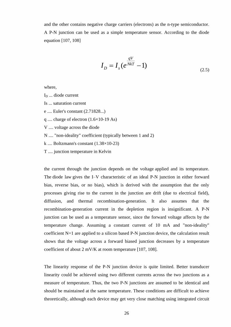
A P-N junction can be used as a simple temperature sensor. According to the diode
equation [107, 108]
( 1)qV
NkTD sI I e
(2.5)
where,
ID ... diode current
Is ... saturation current
e .... Euler's constant (2.71828...)
q .... charge of electron (1.6×10⁻¹⁹ As)
V .... voltage across the diode
N .... "non-ideality" coefficient (typically between 1 and 2)
k .... Boltzmann's constant (1.38×10⁻²³)
T .... junction temperature in Kelvin
the current through the junction depends on the voltage applied and its temperature.
The diode law gives the I–V characteristic of an ideal P-N junction in either forward
bias, reverse bias, or no bias), which is derived with the assumption that the only
processes giving rise to the current in the junction are drift (due to electrical field),
diffusion, and thermal recombination-generation. It also assumes that the
recombination-generation current in the depletion region is insignificant. A P-N
junction can be used as a temperature sensor, since the forward voltage affects by the
temperature change. Assuming a constant current of 10 mA and "non-ideality"
coefficient N=1 are applied to a silicon based P-N junction device, the calculation result
shows that the voltage across a forward biased junction decreases by a temperature
coefficient of about 2 mV/K at room temperature [107, 108].
The linearity response of the P-N junction device is quite limited. Better transducer
linearity could be achieved using two different currents across the two junctions as a
measure of temperature. Thus, the two P-N junctions are assumed to be identical and
should be maintained at the same temperature. These conditions are difficult to achieve
theoretically, although each device may get very close matching using integrated circuit

27
technology [109, 110]. To achieve a P-N junction temperature sensor operated at high
temperatures (above 250°C) is possible, while a low leakage Silicon on Insulator (SOI)
based P-N junction is required. It was also reported that performance of the devices
would deteriorate beyond these high temperature levels, due to a rapid increase in the
diode saturation current [111]. One of the best ways to enhance the sensitivity of p-n
junction temperature sensors is to improve the carrier lifetime. By diffusing gold,
platinum or cobalt atoms deeper to the junctions, carrier lifetime can be improved while
reducing series resistance. The sensitivity is improved because of the dominance of the
diffusion current in the leakage current, while reducing the generation current could be
achieved by increasing carrier lifetime [112].
2.3.2 Humidity Sensor
Humidity is the amount of water vapor in a sample of air compared to the maximum
amount of water vapor the air can hold at any specific temperature. Absolute humidity,
relative humidity and specific humidity are different ways to express the water content
in a parcel of air [113]. Relative humidity (RH) is most frequently used, which is
defined as the ratio of the partial pressure of water vapor in a gaseous mixture of air and
water vapor to the saturated vapor pressure of water at a given temperature. Relative
humidity is expressed as a percentage and calculated in the following manner:
%100*
)(
)(
2
2 OH
OH
P
PRH (2.6)
Where )( 2OHP is the partial pressure of water vapor in the gas mixture; *
)( 2OHP is the
saturation vapor pressure of water at the temperature of the gas mixture; and RH is the
relative humidity of the gas mixture being considered [114].
Humidity sensors can be classified as types of moisture absorption and non-moisture
absorption. The veracity of the sensor should reach ±2% ~ ±5% RH, which would
usually be measured at 20 o
C ± 10 o
C in the clean air. But there are oil, dust and other
gases in the air, which will decrease the long term stability of the sensor. The
temperature sensitivity usually is 0.2~0.8% RH/oC and the sensors usually have a
different temperature sensitivity based on the different RH [115]. There are four kinds
of moisture absorption sensors with the different sensing materials [115-117]:

28
1. Based on dielectric materials, such as lithium chloride. This kind of sensor has a
small hysteresis effect and would not be affected by the speed of wind of the
environment, but the sensitivity would reduce after repeated absorption and
desorption in long term and high relative humidity will make the materials
deliquescent.
2. Based on polymer materials, such as polyimide, fluoropolyol (FPOL),
polyvinyl-alcohol (PVA), and benzocyclobutene (BCB). This kind of sensor has
a small hysteresis and short response time, but cannot be used in the
environment either with organic menstruum or at high temperature.
3. Based on metal oxide films, such as Al2O3, Fe3O4, and tantalum oxides. This
kind of sensor has the advantages of a short response time in the low relative
humidity range, small hysteresis and low cost of fabrication.
4. Based on metal oxide ceramics, such as MgCr2O4-TiO2 ceramic. This type of
sensor has good long term stability and could be effective in the temperature
range of 0~160oC, but oil and dust in the air can contaminate the sensor.
The non-moisture absorption sensors include [115-117]:
1. Sensors based on the thermistor effect which have good reliability and stability.
However, these sensors would not be accurate if the air pressure changed, and
the oil and dust of the air can contaminate the sensor in the long term.
2. Sensors based on the absorption of infrared rays with 1370 nm and 1250 nm
wavelengths which are absorbed by the water vapour.
3. Other kinds of non-moisture absorption sensors, such as optical devices.
Using polymer moisture absorbing layers, capacitance humidity sensors are currently a
hot research topic because of the high sensitivity and easy integration. The operating
characteristics of a typical sensor, SH1100 of Humirel (the humidity sensor business
unit of Measurement Specialties) are shown in Table 2.5 [117].

29
Table 2.5 Characteristics of the SH1100 (Humirel) humidity sensor [117].
Effective range (1%~99%)RH
Capacitance at 55%RH 180pF
Capacitance in 0~100%RH 163pF~202pF
Temperature sensitivity 0.04pF/oC
Response time 5s
Hysteresis 1.5%
Polyimide has been used for capacitive humidity sensors based on MEMS and micro-
fabrication technologies because of its high moisture absorption and easy fabrication
and integration. A typical polyimide-based sensor is shown in Fig. 2.13, with the
sensitivity 0.86 pF/%RH (120 nm polyimide) and 3.4pF/%RH (30 nm polyimide).
Measurements show an offset drift of less than 1% RH at 50% RH and 37oC, and a
hysteresis of ~ 2% RH over a range of 30-70% RH for a 120 nm thick polyimide film
sensor [118].
Figure 2.13 A typical polyimide-based capacitive humidity sensor [118].
A heater has also been integrated with the polyimide-based humidity sensor to shorten
the response time as a thermal reset. A high-sensitivity polyimide-based humidity
sensor is shown in Fig. 2.14, integrated on a polysilicon heater with response time of 1.0
second and a sensitivity of 30.0 fF/%RH. The polyimide sensor has been used to
measure relative humidity levels of up to 80% RH. An accuracy of 3% RH has been

30
obtained using this method, with measurement errors of 0.5oC and 2% RH in
temperature and relative humidity, respectively [119].
Figure 2.14 A polyimide-based humidity sensor integrated on a polysilicon heater [119].
A new material, called divinyl siloxane benzocyclobutene (DVS-BCB or Photo-BCB),
has been used to produce a humidity sensor because of the improvement of sensitivity
and response time. A typical sensor with Photo-BCB as the sensitive material is shown
in Fig. 2.15, in which the sensitivity was increased to 0.19 pF/%RH, and the response
time was decreased to 0.275 second with the sensitive film in thickness of 3.5 µm. In
particular, the performance of the device shows that the sensitivity is better under high
humidity, which is even more relevant for medical applications. The performance of the
sensor could be further enhanced by decreasing the thickness of the film. For a 1.5µm
thick film instead of 3.5 µm, simulation with a dedicated model predicts a sensitivity of
0.39 pF/%RH and a response time of 62 ms [120-122].

31
Figure 2.15 A humidity sensor with PhotoBCB material [120-122].
2.3.3 Pressure/Stress Sensor
Pressure is the force per unit area applied on a surface in a direction perpendicular to
that surface. Stress is also force/area which is applied in different ways without
translation or rotation of the material sample. Stress includes tensile stress which is the
stress state leading to expansion, compressive stress which is the stress applied to
materials resulting in their compaction (decrease of volume), and shear stress which is a
stress state where the stress is parallel or tangential to a surface or interface of the
materials [123-125].
The development of measurement of pressure/stress based on micro-fabrication
technologies began with the discovery of the metal strain gauge. The pressure/stress
sensors could be classified as:
1. strain gauge force sensors;
2. pressure/stress sensors based on piezoresistive effects of materials such as
polysilicon and doped silicon;
3. pressure/stress sensors based on capacity tune detection;
4. pressure/stress sensors based on piezoelectric materials;
5. pressure/stress sensors based on surface acoustic wave (SAW) devices;
6. pressure/stress sensors based on optical detection.
The former three kinds of sensors are easier for integration with other sensors to build
up a multi sensor system.

32
Figure 2.16 Visualization of the working concept behind the strain gauge on a beam
under exaggerated bending [126].
2.3.3.1 Strain Gauge Force Sensors
The strain gauge, invented by Edward E. Simmons and Arthur C. Ruge in 1938, is a
device used to measure deformation (strain) of an object, which is still used in
mechanical transducers. The most common type of strain gauge consists of an insulating
flexible backing which supports a metallic foil pattern. The gauge, shown in Fig. 2.16,
is attached to the object by a suitable adhesive. As the object is deformed, the foil is
deformed, causing its electrical resistance to change. This resistance change is usually
measured with a Wheatstone bridge circuit [126].
Consider a metal filament with a circular cross section. The relative change in resistance
caused by the force is
r
r
l
l
R
R (2.7)

33
where 2r
lR
is the resistance of the filament, l is the length of the filament, r is
the radius of the cross section and is the resistivity of the metal. If the filament is
stretched by an external force F , the stress in the filament is 2r
FT
and the strain
(the relative elongation) in the filament isE
T
l
l
, where E is the Young’s
Modulus of the material.
As well known in mechanics, the longitudinal stretch of a filament is always
accompanied with it a lateral contraction, i.e. l
l
r
r
, where is the Poisson ratio
of the material. So
)21(
R
R (2.8)
The relative change of resistivity,
, is a function of stress/strain and is expressed as
ET , where is the piezoresistive coefficient of the material. Therefore, the
relative change of resistance is,
GER
R
)21( (2.9)
where G, the relative change in resistance per unit strain, is referred to as the gauge
factor, or G factor of the filament. As is negligible for metal materials, the gauge
factor is just a little larger than unity. Because the maximum strain of the gauge is in the
order of 10-3
, the relative change of the resistance is also in the order of 10-3
[127].
2.3.3.2 Pressure/Stress Sensors Based on Piezoresistive Effect
Single crystal silicon has a face-centred cubic crystal structure, which has anisotropic
electrical properties because of the anisotropic structure of the energy band. Ohm's law
for anisotropic silicon materials can be expressed as
34
z
y
x
z
y
x
J
J
J
E
E
E
345
426
561
(2.10)
where E , and J stand for the intensity of electric field, resistivity and current
density respectively. The piezoresistive effect refers to the resistance changes when
stress loaded, which could be displayed as following for single crystal silicon:
6
5
4
3
2
1
44
44
44
111212
121112
121211
6
5
4
3
2
1
00000
00000
00000
000
000
000
T
T
T
T
T
T
(2.11)
where
is the rate of the resistivity change, is the piezoresistive
coefficient and T is loaded stress. In the 32 symmetric parade, just three independent
components are enough for identifying the piezoresistive coefficient which depends on
the doping type, doping concentration and temperature. The piezoresistive coefficients
of silicon at temperature of 300K are shown in Table 2.6 [128, 129].
Table 2.6 Piezoresistive coefficients of silicon at 300K [128, 129].
Si π11 (10-11
/Pa) π12 (10-11
/Pa) π44 (10-11
/Pa)
P type(7.8Ω.cm) 6.6 -1.1 138.1
N type(11.7Ω.cm) -102.2 53.4 -13.6
Heavily doped P+ silicon is usually used for piezoresistive pressure/stress sensors
because of the larger piezoresistive coefficient. In addition, silicon sensors can be
fabricated using both surface fabrication and common MEMS processes. Both the time

35
for diffusion and the energy for implantation can be easily controlled. However, the
resistivity of the P+ silicon has a significant dependence on temperature, which may
affect the sensitivity and the resolution of the sensors.
Polycrystalline silicon (polysilicon) is another kind of piezoresistive material with
considerable enhancement when a phosphorus diffusion source is used instead of boron
dopants for realising piezoresistors. Polysilicon is used as a piezoresistive material also
because of the advantage that the temperature coefficient of resistivity (TCR) can be
made zero by suitably adjusting the doping concentration. However, the sensitivity of
the polysilicon piezoresistor is always lower compared to the monocrystalline
piezoresistor because of the lower gauge factor of polysilicon than that of the
monocrystalline silicon [130]. The gauge factors of different materials are shown in
Table 2.7 [131].
Table 2.7 Gauge factors of different materials [131].
Material Gauge Factor
Metal Foil 1 to 5
Thin film metal ~2
Diffused Semiconductor 80-200
Doped Polysilicon 15-27
The membrane based pressure sensor, shown in Fig. 2.17, is usually fabricated with a
Wheatstone bridge structure, shown in Fig. 2.18, for increasing the sensitivity of the
sensors. The output voltage is related to the change of resistances caused by the
pressure/stress with a positive coefficient for the tensile stress and a negative coefficient
for the compressible stress [132, 133].

36
Figure 2.17 Structure of membrane pressure sensor [132].
Figure 2.18 Wheatstone bridges for piezoresistive pressure sensor [133].
2.3.3.3 Pressure/Stress Sensors Based on Capacitive Detection
In addition to many successful applications in conventional transducers in industry,
capacitive sensing also has many attractive features for MEMS applications. Minimal
additional processes are required using most machining technologies for capacitive
sensors. Capacitors can operate as both sensors and actuators. Excellent sensitivity has
been demonstrated, the transduction mechanism is intrinsically insensitive to
temperature, and the sensitivity of the sensor remains constant with the scaled-down
geometry of the structure.
The theory governing capacitive sensing is the well-established electrostatics. However,
special considerations have to be made for its applications:
As the capacitance of MEMS capacitors is usually small in value, the effects of
stray capacitance and parasitic capacitance are relatively large. Therefore,
special attention has to be paid to these effects in the design of the sensing
structure and circuitry.

37
As micro-mechanical capacitors operate both as sensors and actuators, the
electrical excitation signal for capacitance sensing changes the capacitance being
measured. The effect interferes with the measurement and reduces the signal that
could lead to failure of the capacitance sensors.
The structure of a typical pressure/stress sensor based on capacitance detection is shown
in Fig. 2.19, which has a similar “sandwich” structure to the pressure/stress sensors that
are based on piezoresistive effect [134].
Figure 2.19 Simplified structure of composite-membrane capacitive pressure
sensor[134]
(a) Side view of the sensor structure and (b) cross section of the structure.
The relative capacitance change of the flexible parallel-plate solid-state capacitor
involves the area change of the electrodes and a change in the thickness and relative
dielectric constant of the dielectrics. It can be shown that
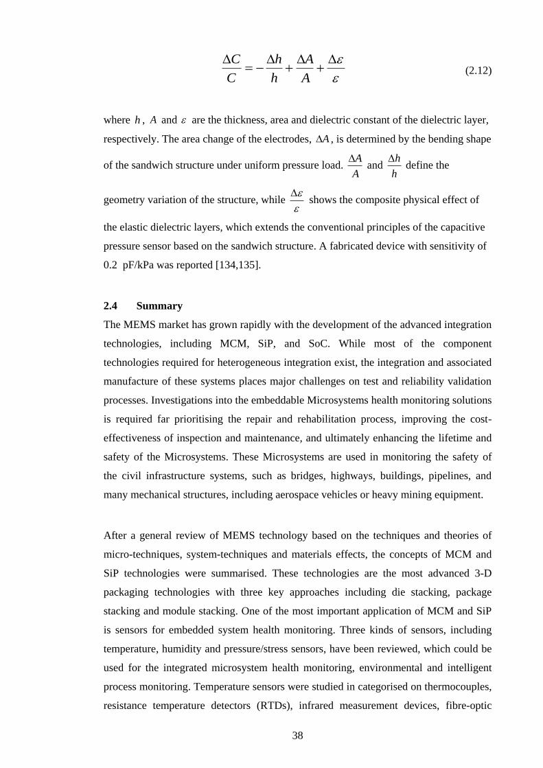
38
A
A
h
h
C
C (2.12)
where h , A and are the thickness, area and dielectric constant of the dielectric layer,
respectively. The area change of the electrodes, A , is determined by the bending shape
of the sandwich structure under uniform pressure load. A
A and
h
h define the
geometry variation of the structure, while
shows the composite physical effect of
the elastic dielectric layers, which extends the conventional principles of the capacitive
pressure sensor based on the sandwich structure. A fabricated device with sensitivity of
0.2 pF/kPa was reported [134,135].
2.4 Summary
The MEMS market has grown rapidly with the development of the advanced integration
technologies, including MCM, SiP, and SoC. While most of the component
technologies required for heterogeneous integration exist, the integration and associated
manufacture of these systems places major challenges on test and reliability validation
processes. Investigations into the embeddable Microsystems health monitoring solutions
is required far prioritising the repair and rehabilitation process, improving the cost-
effectiveness of inspection and maintenance, and ultimately enhancing the lifetime and
safety of the Microsystems. These Microsystems are used in monitoring the safety of
the civil infrastructure systems, such as bridges, highways, buildings, pipelines, and
many mechanical structures, including aerospace vehicles or heavy mining equipment.
After a general review of MEMS technology based on the techniques and theories of
micro-techniques, system-techniques and materials effects, the concepts of MCM and
SiP technologies were summarised. These technologies are the most advanced 3-D
packaging technologies with three key approaches including die stacking, package
stacking and module stacking. One of the most important application of MCM and SiP
is sensors for embedded system health monitoring. Three kinds of sensors, including
temperature, humidity and pressure/stress sensors, have been reviewed, which could be
used for the integrated microsystem health monitoring, environmental and intelligent
process monitoring. Temperature sensors were studied in categorised on thermocouples,
resistance temperature detectors (RTDs), infrared measurement devices, fibre-optic

39
measurement systems and p-n junction temperature sensors. Polymer based humidity
sensors were selected as the focus of the relative humidity (RH) detectors. A summary
of the pressure/stress sensors has been also carried out based on the different sensing
effects, including strain gauge effect, piezoresistive effect, capacity detection,
piezoelectric effect and optical detection.

40
Chapter 3 Design and Fabrication of Thin Film Temperature Sensors
Temperature monitoring is important in many processes and systems as excessive
temperature change can result in detrimental effects and catastrophic failure of
processes and systems. Effective process monitoring methods have been demonstrated
for ultrasonic chemical processes [70] and for wire bonding in electronic manufacturing
[71]. Thin film sensors with small foot print are required for embedded system health
monitoring application, with sensors or sensor arrays being embedded into packages of
SiP based Microsystems. Thin film resistance sensors are ideal for this work, because
they are low cost and are easy to fabricate using thin film deposition and wet or dry
etching methods. Both platinum and nickel based thin film temperature sensors were
studied. Platinum based sensor is mainly used for precise sensing, because it is
relatively expensive and has better linearity of temperature coefficient of resistivity.
Nickel is a relatively cost effective option but offers nonlinear response at higher
temperature. Temperature sensors were studied in range between room temperature
(20 °C) and 375 °C for the applications of both the integrated health monitoring in
microsystems and the process monitoring in laser assisted bonding, where the
temperature above 350 °C would be expected.
3.1 Design and Theoretical Calculation
The meander structure of a metal thin film resistance sensor is shown in Fig. 3.1. The
sensor was designed for high sensitivity within a small effective area. The total
resistance at temperature, T, is given by
0 0 0
( 0.5 )( ) 1 ( ) 1 ( )
n L wR T R T T T T
w h
(3.1)
Figure 3.1 Meander structure of thin film resistance temperature sensor.

41
where R0 is the resistance of the material at a reference temperature (T0), is the
resistivity of the metal being used, L and w are the dimensions of the meander structure,
h is the thickness of the film, and is the temperature coefficient of resistance (TCR),
a constant specific to the metal’s physical properties [136, 137].
The physical properties of platinum and nickel are shown in Table 3.1. The resistance of
the meander platinum thin film device at 293K for length of 10 mm , width of 5 m and
thickness of 100 nm is
4 68 3
0 6 9
10 1010.6 10 2.12 10
5 10 100 10
lR
w h
(3.2)
Then, the temperature dependent response of the resistor is
3
0 0( ) ( 293) 2.12 10 1 0.00392 ( 293)R T R R T T (3.3)
Fig. 3.2 shows the change of resistance as a function of temperature.
Table 3.1 The physical properties of platinum and nickel.
(Source from Comsol 3.3)
Platinum Nickel
Density 21.45103 3/kg m 8.9010
3 3/kg m
Young’s modulus 1.681011
Pa 2.191011
Pa
Poission’s ratio 0.38 0.31
Resistivity 10.610-8
m 6.8410-8
m
Heat capacity 133 /( )J kg K 445 /( )J kg K
Thermal conductivity 71.6 /( )W m K 90.7 /( )W m K
Thermal expansion coeff. 8.8010-6
/ K 13.410-6
/ K
Temperature resistivity coeff. 39.210-4
/ K 68.110-4
/ K

42
Figure 3.2 Calculated response of resistance R(T) as a function of temperature T.
The sensitivity of the temperature sensor under the constant current conditions should
be
0 1 2 0 0 1 21 20 0
1 2 1 2 1 2
( ) ( ) ( )( ) ( ) I R T R T I R T TU T U TI R
T T T T T T
(3.4)
where
0 0.7I mA ,
0 2120R ,
0.00392 (Platinum).
Then the sensitivity is
5.82 /mV K .
The output voltage is
0 0 0( ) ( ) 1 ( 293)U T I R T I R T (3.5)
( 300 ) 1.525U T K V .

43
Fig. 3.3 shows the dependence of the output voltage on temperature.
Figure 3.3 Output voltage versus temperature for a constant current of 0.7mA.
Known as the self-heating effect, heat will be generated and raise the temperature of the
resistor when a current flows through it, which would make the temperature of the
resistor above that of its environment and may introduce an error if a correction is not
made. The power of self-heating is
2 2
0 0 0( ) ( ) 1 ( 293)P T I R T I R T (3.6)
P( 300 ) 1.067T K mW .
The sensitivity under constant voltage conditions should be
0 0
0 2 0 12 1
1 2 1 2
1 ( 293) 1 ( 293)( ) ( )con
con concon con
U UR
R T R R T RI T R I T R
T T T T
(3.7)
where conR is a constant resistance for an output signal of voltage shown in Fig. 3.4.
Both temperature and conR play important parts in the output sensitivity of the
temperature sensor. While 1 2300 ( 300.1 , 299.9 )T K T K T K and 0 2.1 U V , the
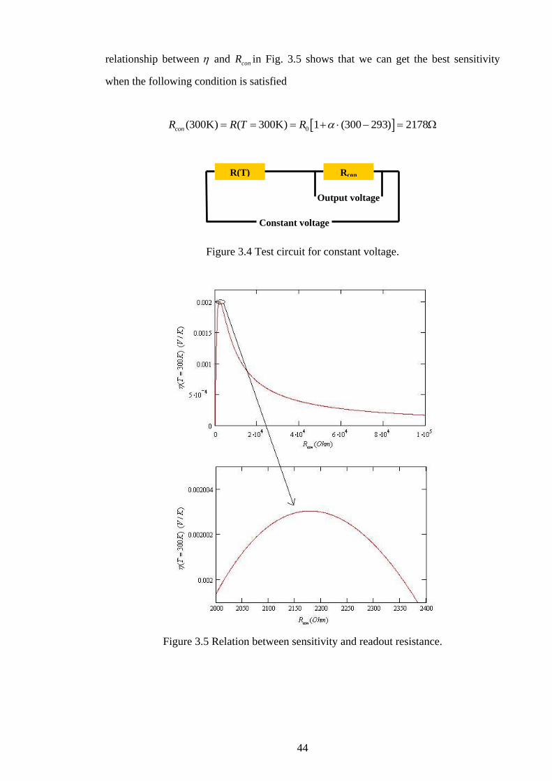
44
relationship between and conR in Fig. 3.5 shows that we can get the best sensitivity
when the following condition is satisfied
0(300K) ( 300K) 1 (300 293) 2178conR R T R
Figure 3.4 Test circuit for constant voltage.
Figure 3.5 Relation between sensitivity and readout resistance.
R(T) Rcon
Constant voltage
Output voltage

45
When
300T K ,
0U 2.1V ,
2178conR ,
the sensitivity of the temperature sensor is
2.00 /mV K .
The output voltage is shown in Fig. 3.6.
Figure 3.6 Output voltages versus temperature with a 2.1 V constant voltage.
The power of self-heating is
2
0
0 con
U( )
1 ( 293) RP T
R T
(3.8)
P( 300 ) 1.012T K mW .
According to these theoretical calculations, a larger resistance of the metal thin film
would offer higher sensitivity for temperature sensors. The output voltage would be
linear for a constant current input but non-linear for a constant voltage input.

46
3.2 Simulation with Finite Element Method
The finite element method (FEM) is a numerical method for finding approximate
solutions of partial differential equations (PDE) and integrals. The method is based
either on eliminating the differential equations completely (steady state problems), or
rendering the PDE into an equivalent ordinary differential equation, which is then
solved using the standard techniques such as finite differences [138].
Making these approximations enables us to solve complex problems with commonly
available computational effect (on a PC). ANSYS is a general-purpose finite element
analysis software, with self contained analysis tools incorporating pre-processing
(geometry creation, meshing), solver and post processing modules in a unified graphical
user interface. ANSYS can be used to solve a wide variety of mechanical problems
including static/dynamic structural analysis, heat transfer and fluid problems, as well as
acoustic and electro-magnetic problems. ANSYS Mechanical incorporates both
structural and material non-linearities. ANSYS Multiphysics includes solvers for
thermal, structural, Computational fluid dynamics (CFD), electromagnetics, acoustics
and can couple these separate physics modules together for multi-disciplinary
applications [139].
Simulations based on ANSYS software have been performed to assist the design of the
metal thin film temperature sensors. The results of simulations are shown in Fig. 3.7
using a 5V of constant voltage. The dimensions of a single unit of platinum thin film are
100 m5m 1m. The sensing temperature and the environment temperatures are
assumed to be 350K and 293K respectively.
According to the simulation, the inside corners of the meander devices exhibit
the maximum temperature. Here the resistance is lower compared with the
outside corners. Rounded corners have the advantage of reducing the
temperature gradient but are more difficult to fabricate at the microscale because
of the photolithography process for small feature (<5 m).
According to Fig. 3.7 (a,b) and (c,e), the average temperatures of 4 units and 12
units of the meander sensor structures are 383.6K and 351.03K, respectively,
without air convection, which shows that the self-heating effect is more
significant in a sensor with a lower resistance, because the lower resistance
resulted in a higher self heating power with the 5V of constant voltage.

47
According to Fig. 3.7 (c,e,g) and (d,f,h), the average temperatures of the 12-unit
meander sensor with and without air convection condition are the same as
351.03K, which shows that the effect of air convection can be ignored for a
sensor with more meanders.
According to Fig. 3.7 (c,d) (e,f) and (g,h), the average temperatures at 1ms, 1s
and 10s after operation are the same, 351.03 K, which shows that the metal thin
film temperature sensor has a quick response time.
(a)Time=0.001s, without air convection (b) Time=1s, without air convection
(c) Time=0.001s, without air convection (d) Time=0.001s, with air convection
(e) Time=1s, without air convection (f) Time=1s, with air convection

48
(g) Time=10s, without air convection (h) Time=10s, with air convection
Figure 3.7 FEM simulation of temperature sensor based on ANSYS.
(Blue scale represents low temperature and red scale represents high temperature)
According to the results of the FEM simulations, a metal thin film resistor with a
resistance of the order of kΩ would be better for both requirements of higher sensitivity
and smaller scale. The self-heating effect should be corrected with calibration curves or
a differential compensation signal. Based on both guidance from analytical calculations
and FEM simulations, the designed dimensions of the meander structures for metal thin
film temperature sensor are shown in Table 3.2, which were selected in order to achieve
a footprint as small as possible. The sensitivities were calculated based on the 0.7mA of
constant current.
Table 3.2 Dimensions design and theoretical sensitivities of temperature sensor

49
3.3 Photomask Design and Manufacturing
A 5-inch photomask was designed using the design software L-Edit (Tanner Research,
Inc.). L-Edit MEMS Design provides unsurpassed capabilities for the design of MEMS,
including all-angle polygon support, complete layer visualization, all-angle design rule
check (DRC), robust algorithm for curved objects, high resolution Encapsulated
PostScript (EPS) output, and full AutoCAD Drawing eXchange Format (DXF)
input/output compatibility. The mask design was manufactured using high quality
chrome film based soda lime glass photomask by Delta Mask, Netherlands. The layout
of the mask, exported from the L-Edit file, is shown in Fig. 3.8. There are 5 kinds of
temperature sensor arrays included in this design, which are shown in Table 3.3. The
photographs of the fabricated sensors from the chrome film based soda lime glass
photomask, taken using an Olympus SZX10 advanced routine stereo zoom microscope,
are shown in Fig. 3.9.
Figure 3.8 Layout of the designed photomask from L-Edit file.

50
Figure 3.9 Photographs of sensor mask
(a) Sensor with track width of 3 m (b) Sensor with track width of 10m.
Table 3.3 Design information of the photomask.
Layout of the photomask
Single sensor 01 (5×)
Single sensor 02
(5×) Multi-Sensor A Multi-Sensor B
Single sensor 03
(5×)
Multi-Sensor E Multi-Sensor E
Multi-Sensor C Multi-Sensor D Single sensor
04A (8×)
Single sensor
04B (8×)
Multi-Sensor E (3×)
Single sensor 05 (5×)
Alignment for KOH/ RIE Silicon
(X-axis)
Design information of the individual sensors
Single-Sensor Length(m) Width(m) Step for dicing
01 10060 3 8450m -X
02 10285 5 3000m -Y
03 10319 7 3000m -Y
(b) (a)

51
04A 15250 10 3000m -Y
04B 25380 10 3000m -Y
05 18600 20 8000m -X
Design information of the multi-sensor arrays
Multi-Sensor Detail of Sensors Dimension of
contact
A Sensor01 (10×) at border with
Sensor04B (3×) central
500m width
except
border central
400m
B Sensor02 (10×) at border
with Sensor04B (3×) central
500m width
except
border central
400m
C Sensor03 (10×) at border
with Sensor04B (3×) central
500m width
except
border central
400m
D Sensor04A (6×) at border
with Sensor04B (3×) central 500m width
E Sensor05 (2×) at border
with Sensor04B (3×) central 700m width
Design information of the contact pads
Pads for Single-Sensor 2mm 2mm
Pads for Multi-Sensor 2.5mm2.5mm

52
3.4 Fabrication and Testing of Nickel Based Temperature Sensors
Nickel was used firstly as the thin film material for the temperature sensors because of
its low cost and high TCR. The sensors with meander structures were fabricated using
the process shown in Fig. 3.10. The nickel thin films were deposited by E-beam
evaporation at 50 mA of electron gun current for 80 seconds. The wafers were cleaned
with DI water and Decon90 liquid before deposition. After spin coating with a 6.5m
of AZ9260 photoresist (6000 rpm for 60 seconds) and baking at 80oC for 4 minutes, UV
photolithography was carried out using the chrome film based soda lime glass
photomask on a mask aligner (Tamarack Model 152R), the exposure dose of which was
370 J/cm2. The nickel etchant, shown in Table 3.4 for detail, was used for nickel
etching.
Figure 3.10 Fabrication process of Ni based temperature sensors.
Table 3.4 Composition of nickel etchant.
Acetic acid 9.375g
Nitric acid 9.375g
Sulfuric acid 3g
DI-water 127.5g

53
The photographs of the fabricated sensors, taken using an Olympus SZX10 advanced
routine stereo zoom microscope, are shown in Fig. 3.11. Sensors in different dimensions
were tested with a multimeter while the sensors were placed on a controlled hotplate
and the temperatures were recorded using a temperature probe. The test results are
shown in Fig. 3.12.
Figure 3.11 Photos of the fabricated Ni temperature sensors.
Figure 3.12 Test results of nickel thin film temperature sensors.
(c) Photo of Multi-Sensor B
(d) Photo of Multi-Sensor E
(b) Sensor with 10m track width (a) Sensor with 5 m track width

54
The behaviour of a sensor with 5m of track width is shown in Fig. 3.13, the sensitivity
of which is about 32.25 mV/K of 0.1 mA with constant current. This is higher than that
of the original design because large initial resistance was obtained while the nickel film
was deposited thinner (<20nm) with the electron beam evaporation process.
Figure 3.13 The resistance response of a sensor with 5m track width.
3.5 Fabrication and Testing of Platinum Based Temperature Sensor Arrays
Fig. 3.14 (a) shows a schematic layout of a thin film microsensor array, which was
designed and fabricated for the embedded accurate temperature monitoring in laser
assisted polymer bonding for MEMS packaging. The layout of the peripheral sensors
was designed to be aligned within the polymer bonding track for monitoring the
bonding temperature. The square polymer ring is illustrated by the track between the
dotted lines. Inside the bonding ring, three sensors are used to monitor the temperature
inside the cavity, providing useful information about the temperature distribution along
with the peripheral sensors placed within the cavity. A lower temperature at the centre
of the cavity is desirable for packaging of temperature sensitive devices. The internal
dimensions of the polymer ring are 4.8 mm × 4.8 mm and the track width is 400 µm.
The thin film resistance temperature sensor arrays are based on meander designs in
order to minimize the sensor size required for this work. Sputtered platinum films on
glass and silicon wafers were used to fabricate the sensor arrays. Table 3.5 shows the
design parameters of the sensors. The track width is the same for all of the peripheral
sensors in an array. Track widths of 3 µm and 5 µm were used for the peripheral
sensors and the width is the same for all of the peripheral sensors in an individual array.
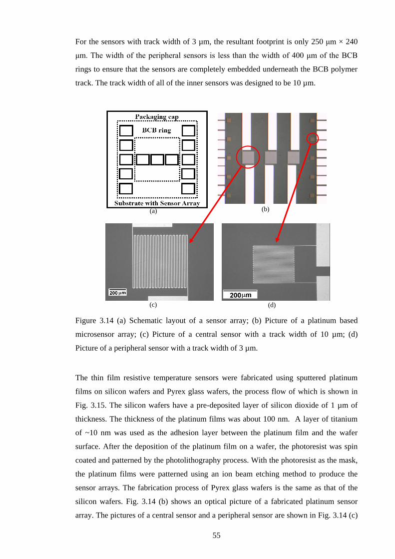
55
For the sensors with track width of 3 µm, the resultant footprint is only 250 μm × 240
μm. The width of the peripheral sensors is less than the width of 400 μm of the BCB
rings to ensure that the sensors are completely embedded underneath the BCB polymer
track. The track width of all of the inner sensors was designed to be 10 µm.
Figure 3.14 (a) Schematic layout of a sensor array; (b) Picture of a platinum based
microsensor array; (c) Picture of a central sensor with a track width of 10 µm; (d)
Picture of a peripheral sensor with a track width of 3 µm.
The thin film resistive temperature sensors were fabricated using sputtered platinum
films on silicon wafers and Pyrex glass wafers, the process flow of which is shown in
Fig. 3.15. The silicon wafers have a pre-deposited layer of silicon dioxide of 1 µm of
thickness. The thickness of the platinum films was about 100 nm. A layer of titanium
of ~10 nm was used as the adhesion layer between the platinum film and the wafer
surface. After the deposition of the platinum film on a wafer, the photoresist was spin
coated and patterned by the photolithography process. With the photoresist as the mask,
the platinum films were patterned using an ion beam etching method to produce the
sensor arrays. The fabrication process of Pyrex glass wafers is the same as that of the
silicon wafers. Fig. 3.14 (b) shows an optical picture of a fabricated platinum sensor
array. The pictures of a central sensor and a peripheral sensor are shown in Fig. 3.14 (c)
(a) (b)
(c) (d)
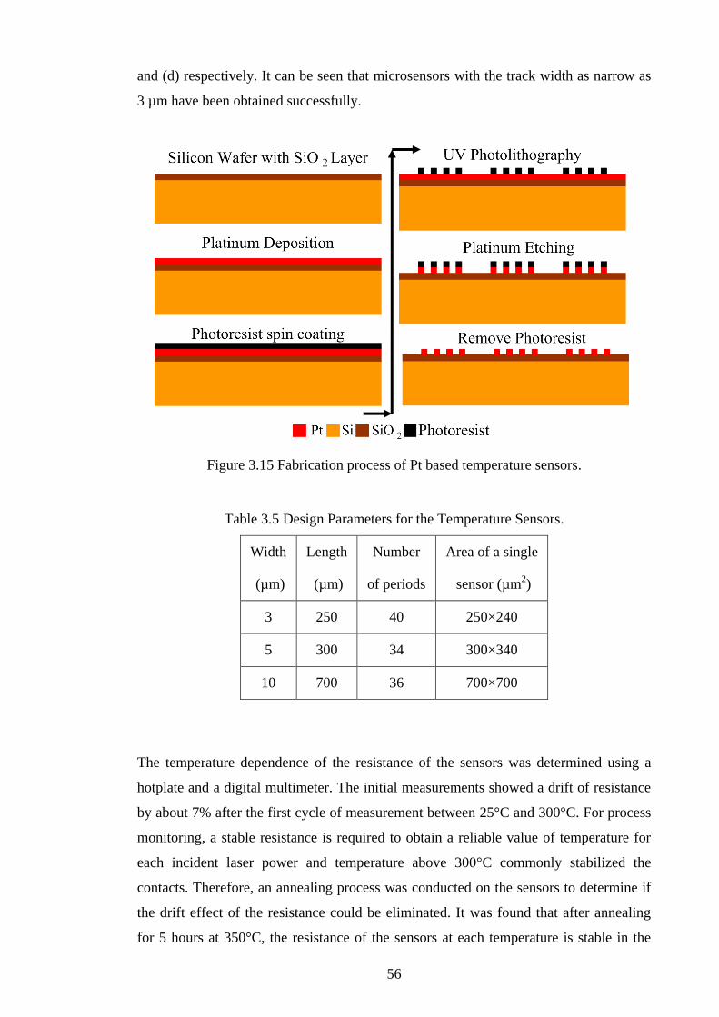
56
and (d) respectively. It can be seen that microsensors with the track width as narrow as
3 µm have been obtained successfully.
Figure 3.15 Fabrication process of Pt based temperature sensors.
Table 3.5 Design Parameters for the Temperature Sensors.
Width
(µm)
Length
(µm)
Number
of periods
Area of a single
sensor (µm2)
3 250 40 250×240
5 300 34 300×340
10 700 36 700×700
The temperature dependence of the resistance of the sensors was determined using a
hotplate and a digital multimeter. The initial measurements showed a drift of resistance
by about 7% after the first cycle of measurement between 25°C and 300°C. For process
monitoring, a stable resistance is required to obtain a reliable value of temperature for
each incident laser power and temperature above 300°C commonly stabilized the
contacts. Therefore, an annealing process was conducted on the sensors to determine if
the drift effect of the resistance could be eliminated. It was found that after annealing
for 5 hours at 350°C, the resistance of the sensors at each temperature is stable in the

57
subsequent temperature cycles of the measurement. Fig. 3.16 shows the linear
behaviour of the thermal responses of the platinum sensors after annealing of sensors
with track width of 3, 5 and 10 µm respectively. The corresponding temperature
coefficients of resistance (TCR) were determined to be from 1.78×10⁻³
/°C to 2.26×10⁻³
/°C at 20°C.
Figure 3.16 Thermal response of platinum sensors.
3.6 Summary
Theoretical studies have been conducted to investigate metal thin film based
temperature sensors. Meander suspended sensors have been designed and modelled
using a commercial FEM simulation software package, ANSYS. The sensor structures,
the effect of self heating and air convection, were extracted from the simulated
solutions. The results show that the inside corners of the meander structures had the
higher temperature, where the resistance is lower compared with the outside corners.
The self-heating effect was less significant in a sensor with a larger resistance. Effect of
air convection could be ignored for a sensor with large resistance.
After the theoretical calculations and the FEM simulations, a 5-inch chrome film based
soda lime glass photomask has been designed and manufactured for the sensor
fabrication. Nickel based sensors were fabricated using electron beam evaporation and
wet etching methods, and platinum based sensors were produced via sputtered

58
deposition and ion beam etching methods. The sensors with meander tracks with widths
of 3 µm have been obtained successfully, resulting in a sensor footprint of 250 μm ×
240 μm. The behaviour of a nickel based sensor with 5 μm of track width shows a
temperature sensitivity of 32.25mV/K with 0.1mA of constant current. After annealing
at 350°C to stabilise the metal films and produce reliable and repeatable measurements,
the corresponding temperature coefficients of resistance (TCR) of the platinum based
sensors were determined to be between 1.78×10⁻³
/°C and 2.26×10⁻³
/°C at 20°C.

59
Chapter 4 Accurate Temperature Monitoring Using an Embedded
Microsensor Array for Laser Bonding
Temperature monitoring is important in many processes and systems as excessive
temperature change can result in detrimental effects and catastrophic failure of
processes and systems. Effective process monitoring methods have been demonstrated
previously for multi-processes [70, 71]. Recently polymer based bonding methods have
become attractive for MEMS packaging since polymer materials such as
benzocyclobutene (BCB) have many desirable properties for packaging applications
including thermosetting, low temperature processing at 250°C ~ 350°C, low moisture
uptake, excellent electrical dielectric properties, and good chemical and thermal
stabilities [139-143]. Extensive studies of BCB bonding for MEMS packaging have
been carried out using conventional heating methods based on heated chucks on a
device or wafer bonder [144-149].
At Heriot-Watt University, a fast laser bonding method using the BCB polymer for
MEMS packaging applications has been demonstrated [150]. Reliable substrate bonding
was achieved in seconds using this method. The laser based approach can
reduce/eliminate the potential damage of devices using rapid, localized heating effects
[150, 151]. However, due to the localized nature of the temperature change, it is
difficult to monitor the precise temperature change within the substrate assembly during
the bonding process. Secondly the thermal response of the substrate assembly under
bonding depends on several factors such as laser power, beam profile, the structures of
the package assembly as well as the design of the bonding setup. Thirdly, precise
temperature monitoring is important for polymers such as BCB as the curing time is
highly dependent on the curing temperature. For BCB, a curing time of several minutes
is required at ~250°C while it is seconds at around 300°C. In the previous work,
conventional methods based on infrared detection [150] and thermo-sensitive paints
[152] were used for temperature monitoring. But these methods could not provide the
precise information about the temperature change within the polymer bonding track and
the temperature distribution within the packaging assembly.
Based on fabricated platinum based temperature sensor arrays, we present the
experimental studies of a temperature monitoring method using an embedded

60
microsensor array in the packaging assembly, for accurate temperature monitoring of
the laser assisted polymer bonding process for MEMS packaging. A diode laser system
with a fibre-coupled output was used in the temperature monitoring experiments.
Custom designed beam shaping optical elements were used to transform the laser beam
into top-hat and frame-shaped beam profiles for energy efficient laser bonding and
investigation of the effect of beam profiles on the resultant temperature change and
distribution.
4.1 The Laser Bonding System
A high power diode laser system with a fibre-coupled output at 970 nm was used as an
energy efficient laser source in the study of the temperature monitoring method using an
embedded microsensor array. Fig. 4.1 shows a schematic of the experimental setup. The
substrate assembly to be bonded using a BCB polymer ring was placed on the bonding
platform. A 0.9 mm thick ceramic plate was used to investigate the effect of thermal
isolation between the bottom substrate and the stainless steel bonding platform.
Figure 4.1 Schematic setup of the bench top laser bonding system.
For energy efficient bonding and investigation of the effect of the beam profile on the
amplitude and distribution of temperature, top-hat and frame-shaped beam profiles were
used in these experiments. The beam profiles were generated using custom designed
planar beam forming optical elements. The beam forming optical element was mounted
in front of the beam delivery module that was coupled to the optical fibre cable from the
laser system. The beam delivery module consists of collimation optics followed by a
focusing lens with a focal length of 20 cm. Fig. 4.2 (a) and (b) show the schematic

61
illustration of the laser beam profiles used in the experiments. It should be noted that
when the capping substrate is transparent the bottom substrate was used to absorb the
laser radiation. Fig. 4.2 (c)-(f) show the images and typical intensity distributions of the
two beam profiles. The dimensions of the top-hat beam for bonding were 6 mm × 6
mm. The outer dimensions of the frame-shaped beam were also 6 mm × 6 mm, most of
the optical power was concentrated in the area of the 1 mm wide ring. It should be noted
that for the frame-shaped beam profile, the beam intensity inside the frame was about
12%~17% of the peak intensity around the frame.
Figure 4.2 (a) Schematic diagram of laser assisted polymer bonding using top-hat beam,
(b) the corresponding schematic diagram using frame-shaped beam, (c) an optical image
of the top-hat beam, (d) typical intensity distribution of the top-hat beam, (e) an optical
image of the frame-shaped beam, and (f) typical intensity distribution of the frame-
shaped laser beam.

62
The frame-shaped beam allows delivery of the laser power to the area of interest for
bonding and, in principle, it is possible to reduce the temperature rise at the centre of the
cavity and therefore reduce the thermal load to the MEMS device to be packaged.
Optical spectroscopic measurements showed the optical transmission of the 500 m
thick silicon substrate at the laser wavelength of 970 nm is negligible. Therefore all of
the laser beam entering the silicon substrate was absorbed and converted to a thermal
effect. The scattering loss of the unpolished backside of the silicon was approximately
20%. The laser power levels stated are values before correction for scattering loss.
4.2 Fabrication of BCB Ring and Pre-alignment of Sensor Array
The polymer sealing rings were fabricated using a photosensitive BCB polymer
(CYCLOTENE 4026-46, Dow Chemical). BCB material can produce a strong and
reliable bond between substrates and has been studied widely for MEMS packaging
applications. A unique characteristic of the BCB polymer is that fast curing can be
realized within a few seconds at temperature of ~300°C instead of minutes at ~250°C
[142, 143]. This fast curing behaviour is ideal for the laser assisted bonding process in
which a rapid temperature rise can be achieved. The BCB sealing rings were produced
on silicon and glass wafers using UV photolithography. Details of the fabrication
process were described previously by our group in Heriot-Watt University [151]. After
fabrication, the wafer was diced into square chips each containing a BCB ring. An
optical picture of a square BCB ring on a glass capping substrate is shown in Fig. 4.3.
The outer dimensions of the BCB ring were 5.2 mm × 5.2 mm and the track width was
400 μm. The thickness of the BCB ring was measured on a ZYGO white light
interferometer and was determined to be ~10 μm.
Figure 4.3 Optical picture of a fabricated BCB ring on a glass cap.

63
In order to obtain good alignment between the BCB polymer ring and the sensor array
for temperature monitoring, the packaging cap was attached to the sensor substrate on a
flip chip bonder in a pre-bonding step prior to laser assisted bonding. The pre-bonding
process was carried out at 100°C for 5 minutes. An optical picture of the pre-bonded
glass-silicon assembly is shown in Fig. 4.4. The substrate assembly consists of a silicon
cap attached to a glass substrate with a sensor array. It can be seen that all of the
peripheral sensors were well placed under the BCB track. Electrical leads were then
attached to the contact pads of the sensors for in-situ temperature monitoring during the
laser assisted bonding experiments.
(a)
(b)
Figure 4.4 (a) Picture of a glass-silicon assembly after pre-bonding
(b) The location of sensors monitored by the data acquisition device.

64
4.3 Embedded Temperature Monitoring of Laser Assisted Bonding
In the temperature monitoring experiments, the top-hat laser beam or frame-shaped
beam generated using the beam forming optical elements was aligned to the polymer
bonding ring. In bonding of glass and silicon substrates the silicon substrate absorbs the
laser radiation and produces the required temperature change to cure the BCB polymer.
In silicon to silicon bonding the capping (top) substrate absorbs the laser radiation. The
sensor array was on the surface of the bottom substrate in all of the experiments. The
resistance change of each sensor as a result of the temperature change was monitored
using a custom designed circuit. The resultant voltage signals from the sensor array
were recorded and displayed on a computer using a data acquisition device (NI-DAQ-
6008, National Instruments).
4.3.1 Bonding Glass Cap to Silicon Substrate
Silicon is one of the most commonly used substrate materials for MEMS fabrication.
The silicon substrates can absorb laser radiation to produce the required temperature rise
for BCB curing when a glass cap is used. In this case the thin film sensor array was
fabricated on the silicon chip and used for in-situ temperature monitoring. The laser
heating was absorbed by the bottom substrates. To improve thermal efficiency, a 0.9
mm thick ceramic plate was placed between the silicon substrate and stainless steel
platform. Fig. 4.5 shows the temporal profiles of the laser induced temperature
monitored by the sensor array. Fig. 4.5 (a) shows the traces of temperature for different
laser powers for both of the top-hat and frame-shaped laser beams. A laser power of 50
W was sufficient to raise the temperature to 300ºC within 50 seconds to cure the BCB
ring, producing a strong bond between the substrates to form a microcavity. Fig. 4.5 (b)
shows the comparison of the temperature between a peripheral sensor and the sensor at
the centre of the array. There is no noticeable difference between the signals for the top-
hat beam indicating that the temperature experienced by MEMS device would be the
same as the bonding temperature. However, as will be shown in the following, the
frame-shaped beam profile can produce a lower temperature at the centre of the silicon
substrate by ~50ºC than the bonding temperature when bonding a silicon cap to a glass
substrate. This is a desirable effect for packaging of temperature sensitive devices.

65
(a)
(b)
Figure 4.5 (a) Temperature profiles of laser bonding between glass cap and silicon
substrate monitored by a peripheral sensor (P), (b) comparison of temperature
characteristics at a laser power of 50 W monitored by a centre sensor (K) and a
peripheral sensor (P).
4.3.2 Bonding Silicon Cap to Glass Substrate
In this case the silicon cap absorbs the laser power to generate the required temperature
for BCB curing. The microsensor array was fabricated on the glass substrate (Pyrex
7740). The bonding arrangement was the same as in the above experiment. Fig. 4.6
shows the measured results of the temperature profiles from the sensors in the array for
the top-hat beam at optical power of 10 W and 20 W respectively. The measured
temperature characteristics were the same for all of the sensors for the top-hat beam.

66
But a temperature difference of about 50°C between that of a peripheral sensor and the
sensor at the centre of the array (P and K in Fig. 4.4 (b) respectively) was seen for the
frame-shaped beam as shown in Fig. 4.7.
(a)
(b)
Figure 4.6 Temperature profiles monitored by the sensors for the top-hat beam at the
laser power of (a) 10 W and (b) 20 W.

67
Figure 4.7 Temperature profiles of bonding silicon cap to glass substrate at a laser
power of 20 W using the frame-shaped beam.
In this bonding configuration the thermal efficiency is much higher than having the
silicon chip as the bottom substrate. An optical power of 20 W was sufficient to produce
a temperature of ~300°C as compared to a required laser power of 50 W when bonding
the glass cap to the silicon substrate, described previously. This is due to the thermal
conductivity of the Pyrex glass being two orders of amplitude lower than that of silicon
so the heat dissipation to the bonding platform is much faster in bonding the glass cap to
the silicon substrate. The thermal conductivities of the substrate materials, the ceramic
plate and the stainless steel platform are given in Table 4.1. The silicon substrates lose
the heat more quickly than the glass substrates.
Table 4.1 Thermal Conductivities of Materials.
Materials Thermal conductivity (W/(m·K))
Silicon 130
Glass (Pyrex 7740) 1.1
Ceramic (Al2O3) 35
Stainless steel 237
4.3.3 Bonding Silicon Cap to Silicon Substrate
Silicon to silicon bonding is desirable in many applications where optical transparency
through the cap is not a requirement. Silicon to silicon bonding has no thermal

68
mismatch between the substrates and therefore eliminates the CTE (coefficient of
temperature expansion) induced stress, thus improving the thermal-mechanical
reliability of the package. In bonding the silicon cap to the silicon substrate, the laser
radiation is absorbed by the top (capping) silicon substrate. This is the same as for
bonding of the silicon cap to the glass substrate described previously.
(a)
(b)
Figure 4.8 (a) Temperature profiles of silicon to silicon bonding monitored by a
peripheral sensor (P), (b) comparison of temperature from a centre sensor (K) and a
peripheral sensor (P) for a laser power of 50 W.
Fig. 4.8 shows the results of temperature monitoring in the laser bonding process. It is
interesting to see that there is little difference between the results for the top-hat and
frame-shaped beam profiles for the same laser power. This is a result of the rapid

69
diffusion of the laser generated thermal energy within the silicon substrates due to the
high thermal conductivity of silicon. The thermal efficiency for the same laser power is
similar to that of bonding a glass cap to a silicon substrate. The result shows that it
requires a laser power of ~ 50 W to produce a temperature rise of ~ 300°C.
4.4 Study of Heat Dissipation Under Substrate Assembly
The effect of thermal dissipation under the bottom substrate was investigated using the
top-hat beam profile for bonding of a silicon cap and a glass substrate at 20 W of laser
power. Three different thermal configurations were used between the bottom substrate
and the bonding platform, including
(1) A 0.9 mm thick ceramic plate,
(2) A 0.5 mm thick silicon wafer and
(3) Without an intermediate thermal barrier between the bottom substrate
and the stainless steel platform.
Figure 4.9 Temperature profiles for different thermal configurations at a laser power of
20 W using the top-hat beam monitored by a peripheral sensor (P).
The results are shown in Fig. 4.9. As expected, it can be seen that the maximum
temperature decreases as the heat dissipation under the sensor substrate increases. This
shows it is useful to add a thermal barrier between the substrate and the bonding
platform in order to improve the efficiency of the laser heating effect. It has been found
that the temperature responses can be described using a single exponential function that
is discussed in the next section. Fig. 4.10 and 4.11 show the corresponding results for
bonding of a glass cap to a silicon substrate and a silicon cap to a silicon substrate

70
bonding respectively. The laser power was 50 W in both cases. Without an intermediate
thermal barrier between the silicon substrate and the bonding platform, a fast rise and
fall of the temperature can be achieved. This thermal behaviour demonstrates the
potential of the bonding method for high speed bonding applications.
Figure 4.10 The effect of heat dissipation under silicon substrate measured by a
peripheral sensor (P) with track width of 3 m on laser induced temperature rise when
bonding to glass cap at 50 W of laser power.
Figure 4.11 The effect of heat dissipation under silicon substrate measured by a
peripheral sensor (P) with track width of 3 m on laser induced temperature rise when
bonding to silicon cap at 50 W of laser power.
It has been found that the experimental results of the temperature characteristics can be
described accurately using the following single exponential function shown in Equation

71
(4.1), where t1 and t2 are the onset and termination time of the laser power, T0 is the
ambient temperature, Ts is the steady state temperature for the given laser power, Ti is
the temperature at the termination time of the laser power, and 1 and 2 are the rise time
and fall time of the laser induced temperature respectively.
(4.1)
By fitting the experimental results presented in Fig. 4.5 – 4.11 using Equation (4.1), the
thermal constants 1 and 2 have been obtained for different substrate assemblies and
heat dissipation configurations. The results are summarized in Table 4.2. The thermal
constants are largely independent of the beam profile, by comparison studying of tests
4&5, 6&7, 8&9, 10&11. The results of test 3&6 and 7&11 show that the thermal
constants are also less dependent on the cap and substrate materials (glass or silicon)
when the bonding process is carried out without the intermediate thermal barrier.
However, the thermal constants are larger for a silicon cap to a silicon substrate bonding
with the ceramic plate between the substrate assembly and the bonding platform, which
are shown in results of test 4&5.
1
1
2
2
0 1
0 0 1 2
0 0 2
,
( ) 1 ,
,
t t
s
t t
i
T t t
T t T T T e t t t
T T T e t t
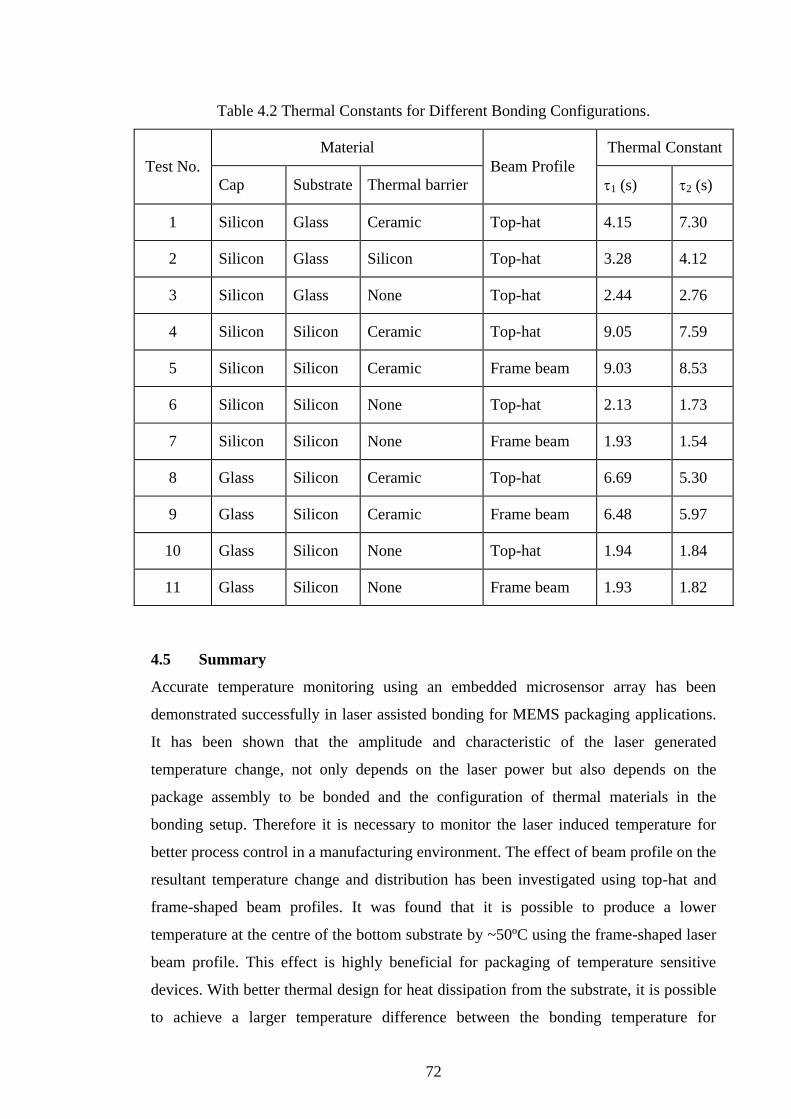
72
Table 4.2 Thermal Constants for Different Bonding Configurations.
Test No.
Material
Beam Profile
Thermal Constant
Cap Substrate Thermal barrier 1 (s) 2 (s)
1 Silicon Glass Ceramic Top-hat 4.15 7.30
2 Silicon Glass Silicon Top-hat 3.28 4.12
3 Silicon Glass None Top-hat 2.44 2.76
4 Silicon Silicon Ceramic Top-hat 9.05 7.59
5 Silicon Silicon Ceramic Frame beam 9.03 8.53
6 Silicon Silicon None Top-hat 2.13 1.73
7 Silicon Silicon None Frame beam 1.93 1.54
8 Glass Silicon Ceramic Top-hat 6.69 5.30
9 Glass Silicon Ceramic Frame beam 6.48 5.97
10 Glass Silicon None Top-hat 1.94 1.84
11 Glass Silicon None Frame beam 1.93 1.82
4.5 Summary
Accurate temperature monitoring using an embedded microsensor array has been
demonstrated successfully in laser assisted bonding for MEMS packaging applications.
It has been shown that the amplitude and characteristic of the laser generated
temperature change, not only depends on the laser power but also depends on the
package assembly to be bonded and the configuration of thermal materials in the
bonding setup. Therefore it is necessary to monitor the laser induced temperature for
better process control in a manufacturing environment. The effect of beam profile on the
resultant temperature change and distribution has been investigated using top-hat and
frame-shaped beam profiles. It was found that it is possible to produce a lower
temperature at the centre of the bottom substrate by ~50ºC using the frame-shaped laser
beam profile. This effect is highly beneficial for packaging of temperature sensitive
devices. With better thermal design for heat dissipation from the substrate, it is possible
to achieve a larger temperature difference between the bonding temperature for

73
packaging and the temperature experienced by the device being packaged. It was found
that the temperatures characteristics can be described using a single exponential
function. The thermal constants are largely independent of the beam profiles but highly
dependent on the thermal arrangement of the materials underneath the bottom substrate.
An intermediate ceramic plate between the substrate and the stainless steel bonding
platform can improve the thermal efficiency of the bonding laser power significantly.
74
Chapter 5 BCB Film Based SAW Humidity Sensor
Surface acoustic wave (SAW) devices are attractive for use in humidity sensors because
of their small size, low cost, high stability, short response time, high sensitivity, good
reliability, good reproducibility and capability of compatibility with the integrated
circuit process. Moreover, the fabrication of SAW humidity sensors is much simpler
and easier than the capacitive or resistive humidity sensor, using only one step
photolithography instead of producing the parallel plate capacitors or the expensive ion
implantation/diffusion processes. A SAW based humidity sensor has been proposed to
be integrated as one of the multi-sensors for embedded health monitoring in SiP based
Microsystems. Instead of the conventional polymer based moisture absorbing layer,
such as polyimide, fluoropolyol (FPOL), and polyvinyl-alcohol (PVA), the
benzocyclobutene (BCB) polymer has been investigated as the sensing film for
absorbing moisture [120-122]. Using changes in mass loading due to the uptake of
moisture by the polymer, changes in relative humidity (RH) levels resulting in the shift
of both centre frequency and amplitude of the SAW resonators have been measured.
The SAW resonators have been fabricated with metal interdigital transducer (IDT)
fingers based on piezoelectric substrates [120-122, 153-156].
5.1 BCB and Moisture Capture
CYCLOTENE, a series of advanced electronics resins from the Dow Chemical
Company (USA), are high-purity polymer solutions that have been developed for
microelectronics applications, which include wafer-level chip-scale packaging,
dielectric isolation for multilayer interconnects, strong and void-free bonds for MEMS
and 3D integration, printed circuit board technology, integrated passives/radio
frequency (RF) components, active matrix liquid crystal displays, passivation/stress
buffer, etc.. The resins are derived from B-staged bisbenzocyclobutene-based (BCB)
monomers and are formulated as high-solids, low-viscosity solutions. The chemical
formula of BCB and chemical equation of polymerization reaction are shown in Fig. 5.1
[142, 143].
The BCB based humidity sensing technology has already been studied and applied in
monitoring the humidity level of human breath as well as in a pulmonary function
diagnosis Microsystem [157-159]. For the convenience of using UV photolithography

75
processes as well as the resource availability, CYCLOTENE 4026-46 has been selected
from the CYCLOTENE 4000 series advanced electronic resins. These resins come as I-
line (365 nm), G-line (436 nm), and broad band-sensitive photopolymers. The electrical
and thermal properties of Photo-BCB (CYCLOTENE 4000 resin series) are shown in
Table 5.1, while the mechanical properties of photo-BCB are shown in Table 5.2 [142,
160]. The polymer resins have been used in the fabrication of a SAW based humidity
sensor.
Figure 5.1 BCB formula and chemical crosslink equation.
Table 5.1 Electrical and thermal properties of Photo-BCB [142, 160].
Property Value
Dielectric constant (1kHz – 20GHz) 2.65
Dissipation factor 0.0008
Breakdown voltage 5.3 MV/cm
Leakage current 4.7 × 10⁻¹⁰
A/cm2 at 1.0 MV/cm
Volume resistivity 1 × 10¹⁹
Ω-cm
Thermal conductivity 0.29 W/mK at 24°C
Thermal stability 1.7% weight loss per hour at 350°C
Monomer formula Diene synthesis
Dimer
Highly crosslinked structure

76
Table 5.2 Mechanical properties of Photo-BCB [142, 160].
Property Value
Coefficient of thermal expansion 42 ppm/°C at 25°C
Glass transition temperature >350°C
Tensile modulus 2.9 ± 0.2 GPa
Tensile strength 87 ± 9 MPa
Elongation at break 8 ± 2.5%
Poisson ratio 0.34
Stress on Si at 25°C 28 ± 2 MPa
Table 5.3 Recommended storage temperatures and times [142, 160].
Storage need Temperature Shelf Life
Long term Freezer (-15°C) 1 year from date of manufacture
Medium term Refrigerator (4°C) 1-2 months
Short term Clean room (20°C) 5 days
As photosensitive CYCLOTENE resin ages, the spun-on thickness will gradually
increase as the resin becomes more viscous due to solvent evaporation. The lifetime is
based on the criterion of less than 5% change in thickness. Resins should be allowed to
equilibrate to room temperature before use. Recommended storage conditions and times
are shown in Table 5.3. Several process options are available for CYCLOTENE 4000
series, and two of the typical process flows are shown in Fig. 5.2. Process A uses a hot
plate soft bake and includes a develop end point monitor, and process B uses a hot plate
soft bake and a pre-develop bake to stabilize the develop end point, while an oven soft
bake is also possible. A spin coating was used for coating the BCB polymer onto the
substrates. By increasing the spinning speed, the desired pre-exposure thickness could
be achieved, the details of which are shown in Table 5.4 [142, 160].

77
Figure 5.2 Process Flows for CYCLOTENE 4000 Series Resins [142, 160].

78
Table 5.4 Typical thickness of CYCLOTENE 4000 series polymers (4022-35, 4024-40
and 4026-46) after spin coating [142, 160].
4022-35
thickness (μm)
4024-40
thickness (μm)
4026-46
thickness (μm)
Spin speed
(rpm)
After
soft bake
Final
thickness
(hard bake)
After
soft bake
Final
thickness
(hard bake)
After
soft bake
Final
thickness
(hard bake)
1500 6.9 5.2 10.2 7.2 18.5 14.2
2000 5.8 4.3 8.4 5.9 15.2 11.6
2500 5.2 3.8 7.4 5.2 13.3 10.2
3000 4.7 3.4 6.7 4.8 12.2 9.4
3500 4.4 3.1 6.2 4.4 11.3 8.7
4000 4.1 2.9 5.8 4.1 10.6 8.1
5000 3.7 2.6 5.2 3.7 9.4 7.3
Table 5.5 Equilibrium wt % water in Photo-BCB at various RH at 23°C [142, 160].
CYCLOTENE resin Film thickness (μm) Relative Humidity (%)
30 54 84
4024-40 5 0.061 0.075 0.14
4026-46 10 0.058 0.077 0.14
4026-46 20 0.050 0.082 0.14
Compared to epoxy resins, polyamides and other microelectronic polymers, BCB is
well accepted because of its excellent properties such as water absorption (0.12% at
80% RH), planarization (e.g. > 90% for CYCLOTENE 3022), dielectric constant (2.5 at
1-10 GHz), dielectric loss at high frequency (e.g. 0.002 at 1-10 GHz), rapid curing (e.g.
one minute on a hot plate under nitrogen), and copper compatibility [162]. The moisture
absorbing abilities, water weight percentage based on the total weight of the Photo-BCB
polymer films, are shown in Table 5.5 [142, 160].

79
According to the reported studies of BCB based capacitive humidity sensing, soft cured
aqueous developable PhotoBCB offered an increase of 17.1% for the moisture solubility,
and gave the highest sensitivity of the humidity sensors. Hard cured BCB gave an
increase of 40.3% for moisture diffusivity, while giving the fastest sensing response of
the humidity sensors. All the comparisons were made based on the reference of hard
cured Cyclotene 4024 resin [156]. Both moisture solubility and diffusivity should be
considered for the performance of the humidity sensors, which can be compared in
terms of their sensitivity as well as their response time. Cyclotene 4024-40 has the
advantages of linear moisture sorption isotherms and the large diffusion coefficient for
water (4.5±0.5m2s
-1 at 23°C). Both the physical and behavioural models of transient
responses of the capacitive humidity sensors have also been presented, which were
supported by finite element method (FEM) simulation as well as experimental
validation [120, 121]. A full film oxidation process has also been used. Both the
sensitivity and the response time have been improved significantly by complete bulk
oxidation of the DVS-BCB / Photo-BCB sensitive film. The device with a film
thickness of 3.5 m successfully showed a sensitivity of 0.19 pF/%RH and a response
time of 0.275 second, while simulation results of the sensor with 1.5 m thick film
showed an enhanced sensitivity of 0.39 pF/%RH and a response time of 0.062 second
[120].
5.2 Piezoelectric Effect and Lithium Niobate Substrates
A surface acoustic wave (SAW), first explained by Lord Rayleigh in 1885, is a kind of
acoustic wave traveling along the surface of a material exhibiting elasticity, whose
amplitude typically decays exponentially with depth into the substrate. By using the
piezoelectric materials, the transduction from electric energy to mechanical energy is
easily accomplished, e.g. piezoelectric materials will be deformed when a voltage is
applied [163].
5.2.1 Piezoelectric Effect
The piezoelectric effect, first directly demonstrated by brothers Pierre Curie and Jacques
Curie in 1880, is the ability of a material to produce electricity when it is subjected to
mechanical stress. This effect also works in reverse, as materials can be deformed
slightly when subjected to an applied voltage [164]. Based on the piezoelectric effect,
crystal structures of piezoelectric materials bend in different ways, which result in
different vibration modes with different vibration frequencies in the range of KHz to

80
GHz. Table 5.6 shows the vibration modes and the frequencies, which are widely used
for sensing applications [165].
Table 5.6 Various vibration modes of different piezoelectric materials [165].
Piezoelectricity is the combined effect of the material’s electrical and mechanical
behaviour:
D E (5.1)
where D is the electric charge density displacement, ε is permittivity and E is electric
field strength.
Meanwhile, according to the Hooke's Law:
S sT (5.2)
where S is strain, s is compliance and T is stress.

81
Equation (5.1) and (5.2) may be combined into the strain-charge equations:
[ ] [ ] E tS s T d E (5.3)
[ ] [ ] TD d T E (5.4)
where [ ]d is the matrix for the direct piezoelectric effect and [ ]td is the matrix for the
converse piezoelectric effect. The superscript E indicates a zero or constant electric field,
the superscript T indicates a zero or constant stress field, and the superscript t stands
for transposition of a matrix.
The strain-charge equations for materials in tetragonal crystal structures or Hexagonal
crystal structures may also be written as:
1 1 3111 12 13
2 2 3221 22 23
3 3 3331 32 33
4 4 2444
5 5 1555
6 666 11 12
0 00 0 0
0 00 0 0
0 00 0 0
0 00 0 0 0 0
0 00 0 0 0 0
0 0 00 0 0 0 0 2( )
E E E
E E E
E E E
E
E
E E E
S T ds s s
S T ds s s
S T ds s s
S T ds
S T ds
S Ts s s
1
2
3
E
E
E
(5.5)
1
2
1 15 11 1
3
2 24 22 2
4
3 31 32 33 33 3
5
6
0 0 0 0 0 0 0
0 0 0 0 0 0 0
0 0 0 0 0
T
TD d E
TD d E
TD d d d E
T
T
(5.6)
where Equation (5.5) represents the relationship for the converse piezoelectric effect
and Equation (5.6) represents the case for the direct piezoelectric effect [164, 166].

82
5.2.2 Lithium Niobate Substrates
Among the family of piezoelectic substrate materials, quartz (SiO2), lithium tantalate
(LiTaO3), and lithium niobate (LiNbO3) are most commonly used for acoustic wave
sensors and devices. Table 5.7 lists some relevant specifications for each material,
including the most popular cuts and orientations. There are also other kinds of
piezoelectric materials with commercial potential, including gallium arsenide (GaAs),
silicon carbide (SiC), langasite (LGS), zinc oxide (ZnO), aluminum nitride (AlN), lead
zirconium titanate (PZT), polyvinylidene fluoride (PVdF), etc. [167].
Table 5.7 Physical parameters of commonly used piezoelectric materials [167].
Material Orientation
Velocity
of SAW
(m/s)
Temperature
coefficient
(ppm/oC)
Attenuation
at 1 GHz
(dB/S)
Quartz Y, X 3159 -24 2.6
Quartz ST, X 3158 0 3.1
Lithium Tantalate Y, X 3230 35 1.14
Lithium Tantalate 167 rotation 3394 64 -
Lithium Niobate Y, Z 3488 94 1.07
Lithium Niobate 128 rotation 3992 75 -
At a higher wave velocity of 3992 m/s, SAW devices fabricated on Lithium Niobate
substrates performed at the higher resonating frequencies than other common
commercial piezoelectric materials. This results in a higher sensitivity of the SAW
based sensors. As one of the most attractive materials, lithium niobate has desirable
properties such as piezoelectric, electro-optic, photoelastic, non-linear optic, good
mechanical and chemical stability, and wide transparency spectra range. The main
properties of lithium niobate are shown in Table 5.8. LiNbO3 has been widely used as
frequency doubling material, for Q-switches, waveguide substrates and surface acoustic
wave (SAW) devices [168– 171].

83
Table 5.8 Main properties of lithium niobate [171].
Property Value Notes
Optical index or refraction (o-axis) 2.21 At λ=1.55m
Optical index or refraction (e-axis) 2.14 At λ=1.55m
RF dielectric coefficient (o-axis) 42.5 ≈ constant from 100MHz to 140 GHz
RF dielectric coefficient (e-axis) 26 ≈ constant from 100MHz to 140 GHz
RF refractive index (o-axis) 6.5 ≈ constant from 100MHz to 140 GHz
RF refractive index (e-axis) 5.1 ≈ constant from 100MHz to 140 GHz
Electrical conductivity 1×10-18
/Ωcm At DC
Thermal conductivity 5.6 W/moC
Thermal expansion (o-axis) 14×10-6
/oC
Thermal expansion (e-axis) 4×10⁻⁶
/oC
Thermal effect on index (o-axis) 1.8×10⁻⁶
/oC
1 o
o
dn
n dT
Thermal effect on index (e-axis) 1.60×10⁻⁶
/oC
1 e
e
dn
n dT
Melting point 1253 oC
Density 4.635 g/cm3
Band gap 4 eV
Electro-optic coefficient
r33=30.8 pm/V
r13=30.8 pm/V
r22=30.8 pm/V
r51=30.8 pm/V
22 13
22 13
33
51
51
22
0
0
0 0
0 0
0 0
0 0
ij
r r
r r
rr
r
r
r
Nonlinear electro-optic coefficient
d31=11.6
d33=86
d22=5.6
Piezoelectric strain coefficient
d15=69.20 pm/V
d22=20.80 pm/V
d31=-0.85 pm/V
d33=6.00 pm/V
15 22
22 22 15
31 31 33
0 0 0 0
0 0 0
0 0 0
ij
d d
d d d d
d d d

84
Normally, lithium niobate can be specified into three grades based on its different
applications, acoustic (SAW) grade, refractive grade, and optical grade. Acoustic grade
is the most commonly produced grade for making SAW based devices, and is also the
least demanding in terms of impurities and crystalline perfection because of its non-
optical applications. The crystals are grown over quite a long time, converting a large
fraction of the melt into crystalline material [168, 170].
Regular lithium niobate is strongly pyroelectric. The surface of regular lithium niobate
substrates may accumulate electric charge when substrates are heated or cooled during
the soft bake and hard bake steps during the UV photolithography process. This may
cause spontaneous electrical discharge between dense metalized lines on the substrate,
such as the IDTs of SAW devices, as well as electrical discharge between the substrate
and the metal plate used for heating or cooling. This discharge effect makes the regular
lithium niobate substrates difficult for wafer handling and processing, and may cause
the substrate to be damaged. Meanwhile, the wide transparency spectra range of regular
lithium niobate may also bring yield effects including multi-reflection and scattering in
the UV photolithography process.
Chemical reduction, at elevated temperatures in an environment of nitrogen and
hydrogen, produces chemically reduced lithium niobate (black lithium niobate) material
which has an increased electric conductivity, of the order of 104, and effectively
eliminates pyroelectric sparking. At the same time, the optical absorption is increased
significantly causing its appearance to become gray to dark black and almost non-
transparent, which has a positive impact on the photolithography process. A picture of
the black lithium niobate wafers is shown in Fig. 5.3, the advantages of which include:
Good ability to neutralise electrical charges even if the applied electrical
potential occurs instantaneously;
No difference in piezoelectric properties from regular lithium niobate wafers;
High uniformity of bulk resistivity in the surface and bulk of wafers.
The typical properties of black lithium niobate wafers are shown in Table 5.9 [172-176].

85
Table 5.9 Typical properties of lithium niobate wafers [172-176].
Black lithium niobate Regular lithium niobate
Bulk Resistivity (Ω · cm) 2.40E+11 3.80E+14
Bulk Conductivity (Ω-1
· cm-1
) 4.17E-11 2.63E-15
Surface Electric Potential*
/100mmφ(kV) <0.05 3.05
Electrical Charge
neutralisation (sec) 1.5 ∞
Optical Transmission%# <60 73
Colour Dark Grey Colourless
Lithium Niobate 127.86 ° Y-cut
Black lithium niobate Regular lithium niobate
Curie temperature Tc (°C) 1132±2 1132±2
SAW velocity Unchanged 3980
Coupling coefficient k2 Unchanged 5.5
* Electrical charges due to temperature rising from room temperature to 95°C at 4-inch wafer # 0.35mm thickness wafer (with both sides mirror polished) measured by 365nm wavelength
Figure 5.3 Picture of black lithium niobate wafers [176].
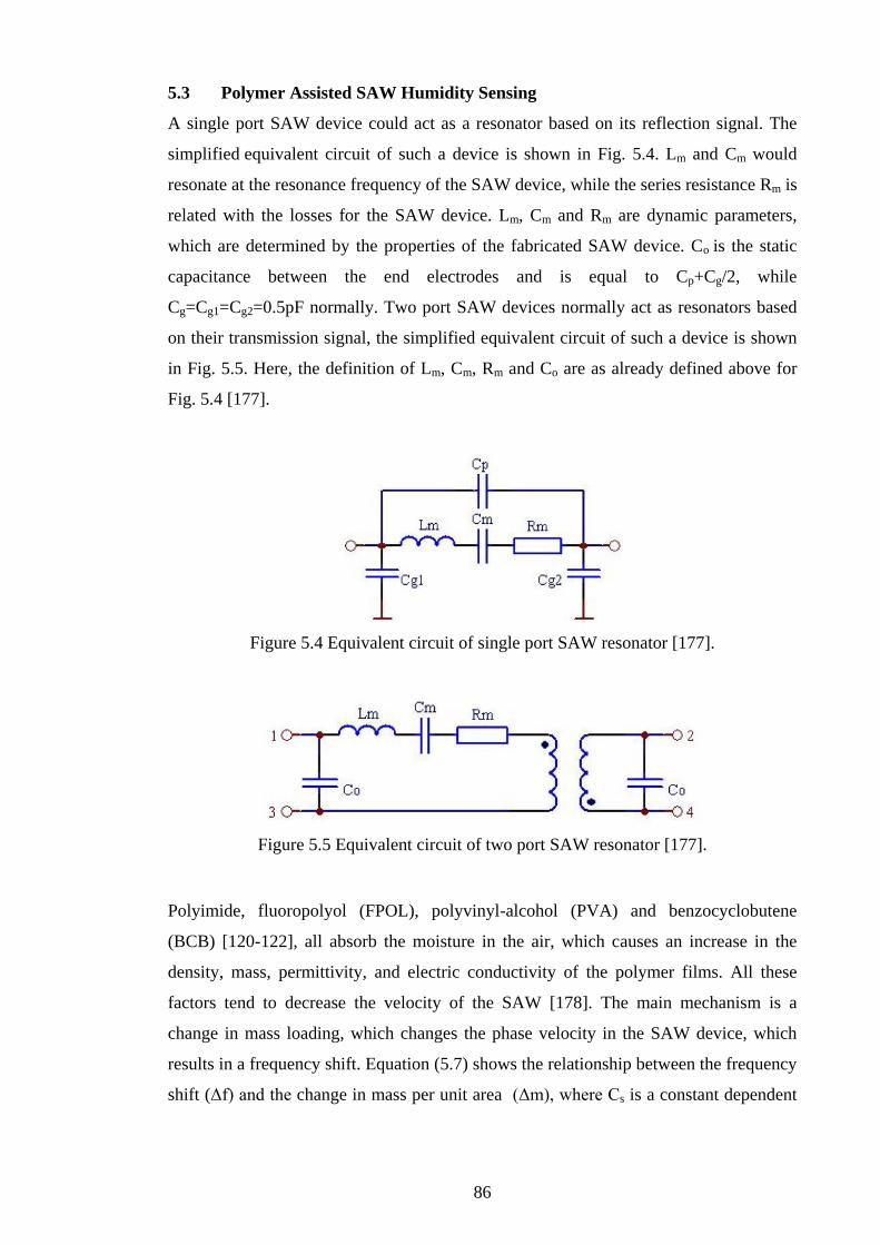
86
5.3 Polymer Assisted SAW Humidity Sensing
A single port SAW device could act as a resonator based on its reflection signal. The
simplified equivalent circuit of such a device is shown in Fig. 5.4. Lm and Cm would
resonate at the resonance frequency of the SAW device, while the series resistance Rm is
related with the losses for the SAW device. Lm, Cm and Rm are dynamic parameters,
which are determined by the properties of the fabricated SAW device. Co is the static
capacitance between the end electrodes and is equal to Cp+Cg/2, while
Cg=Cg1=Cg2=0.5pF normally. Two port SAW devices normally act as resonators based
on their transmission signal, the simplified equivalent circuit of such a device is shown
in Fig. 5.5. Here, the definition of Lm, Cm, Rm and Co are as already defined above for
Fig. 5.4 [177].
Figure 5.4 Equivalent circuit of single port SAW resonator [177].
Figure 5.5 Equivalent circuit of two port SAW resonator [177].
Polyimide, fluoropolyol (FPOL), polyvinyl-alcohol (PVA) and benzocyclobutene
(BCB) [120-122], all absorb the moisture in the air, which causes an increase in the
density, mass, permittivity, and electric conductivity of the polymer films. All these
factors tend to decrease the velocity of the SAW [178]. The main mechanism is a
change in mass loading, which changes the phase velocity in the SAW device, which
results in a frequency shift. Equation (5.7) shows the relationship between the frequency
shift (Δf) and the change in mass per unit area (Δm), where Cs is a constant dependent

87
on the properties of the piezoelectric substrate of the SAW device and 0f is the
resonance frequency of the SAW device [179-181].
2
0sf C f m (5.7)
Meanwhile, the amplitude of the SAW resonant signal would change with the amount
of energy dissipated into the medium contacting the device surface. The physical
properties of coated polymers which act as the surface contacting medium would also
be changed on absorbing moisture, resulting in amplitude changes. These changes are
reflected in the insertion loss, which is defined as the ratio of the output signal
amplitude to that of the input, in decibels. The total energy loss across the device
includes transduction losses, propagation losses (occurring as the waves travel through
the piezoelectric material of the device), and additional losses from dissipation of
energy in the medium contacting the device surface [179].
The behaviour modelling of the SAW device has already been studied using several
methods, including the impulse response method, the conventional matrix approach and
the modified matrix approach. As a baseline for modelling the SAW device, the impulse
response method is valid only for transducers where at least one of the two IDTs has a
constant aperture or finger overlap. This modelling approach includes both mechanical
and electrical behaviour of SAW devices, including frequency response, the loss of the
system, the admittance, and the parameters for circuit simulators. Constant equal
spacing and finger width are normally assumed. The conventional matrix method is
based on transmission line theory. The SAW device is modelled as two IDTs with two
ports for mechanical waves travelling into and out of the IDT when current and voltage
are on the IDTs. The matrix for SAW delay line is simply the multiplication of the
matrices for the two IDTs and a matrix for the delay in between. The complete SAW
device matrix normally is given by:
1 2[ ( )] [ ( ) ( ) ( )]SAW f T f D f T f (5.8)
where f is the frequency, 1( )T f and 2 ( )T f are the transmission matrices for each IDT
which can be cascaded easily, and ( )D f stands for the delay matrix [182-184].

88
Based on both the impulse response method and the conventional matrix approach, the
model has been extended by including second order elements. In this approach, The
model divides an IDT into half wavelength sections, which are further divided into
zones. Two of the zones are un-metalized areas (1/8 of a wavelength) around one zone
that is comprised of a metal finger (1/4 of a wavelength). While each zone is modelled
by a transmission line matrix, the SAW delay line matrix is simply the multiplication of
the matrices for the two IDTs and the delay or space between the IDTs [182, 183].
The power consumption analysis of the SAW sensor system was reported in 2006,
modelled using the software of ANSYS and PSPICE [185]. There are several design
parameters of the SAW sensor, including the distance between two IDTs, thickness of
piezoelectric substrate and finger space of IDT. All of these could significantly affect
the power consumption of the full sensing system. The simulated results show that the
total power consumption increases as the centre distance between each IDT increases.
The reason for this is that more power will be lost during transporting from one IDT to
another with increasing the centre distance. The study of the power consumption caused
by different thickness of the piezoelectric substrates shows that there is no variation in
the transverse direction along the surface and that the particles move both in the
direction of wave propagation and perpendicular to the depth of substrate, while the
surface waves propagate along the surface and decay into the bulk material within a
distance of the order of a wavelength. These simulation results demonstrate that the
maximum wave amplitude occurs at 1/4λ thickness due to the interference from the
back surface of the substrate, which corresponds to the maximum power of SAW
transportation. The value of the finger space will also affect the total system power
consumption, which also determines the resonance frequency of the SAW sensor. The
simulation results show that the power consumption decreases as the resonance
frequency increases. This also means reducing the distance between two adjacent
fingers within the single IDT, the limit of which depends on the resolution of the
lithography fabrication process [185-188].
5.4 Design and Fabrication of SAW Based Sensors
To achieve the transduction from electrical energy to mechanical energy, SAW based
devices are normally designed and fabricated by patterning metal IDTs on piezoelectric
substrates in arrays of single or pair of IDTs. SAW devices have been in commercial
use for more than 60 years for applications in filters, oscillators, transformers, as well as

89
applications in sensing and microfluidics. A schematic picture of a typical SAW device
design is shown in Fig. 5.6 [167].
Figure 5.6 Schematic picture of a typical SAW device design [167].
The width of the individual IDT was designed to be the same dimension as the gaps
between the IDTs, both of which are a quarter of the wavelength of the SAW resonator.
For example, the wavelength of the SAW resonator was 16 m while the width of the
individual IDT was designed as 4 m. This yields a resonance frequency of about
249.50 MHz, when the SAW velocity is 3992 m/s based on the Equation (5.9), where
f is the resonance frequency, v is the wave velocity, and is the wavelength. The
number of IDTs in each transducer determines the power of the wave generated, while
longer IDTs provide more uniformity on the wave travelling direction. A normalized
metal thickness range for the IDTs was designed from 0.4% to 4% of the wavelength
[189].
vf
(5.9)
The reflection grating structures have also been considered for enhancing the amplitude
of the resonance. The maximum reflectivity of a shorted grating (shown in Fig. 5.7a) is
slightly higher than that of an open grating (shown in Fig. 5.7b) [189].

90
(a)
(b)
Figure 5.7 SAW transducer with (a) shorted grating reflector, (b) open grating reflector.
A 5-inch photomask was designed using the design software L-Edit (Tanner Research,
Inc.). the mask was produced by Delta Mask (Netherlands) with patterned Cr film on a
soda lime glass substrate. The layout of the mask, exported from the L-Edit file, is
shown in Fig. 5.8, which includes 4 single and 9 dual SAW resonators. The SAW
resonators were designed with IDTs widths of 4, 8, and 16 µm, and lengths of 2.9, 3.9
and 4.9 mm with distances between the SAW transducers of 1.5, 2, 3, 4, and 5 mm
being used. The reflection grating structures were also included in the mask design.
More detailed information of the photomask design is shown in Table 5.10 and 5.11.
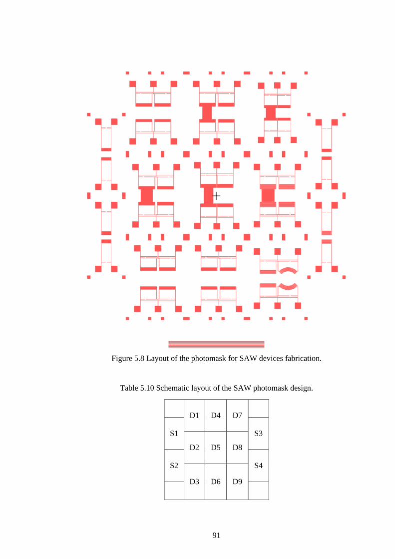
91
Figure 5.8 Layout of the photomask for SAW devices fabrication.
Table 5.10 Schematic layout of the SAW photomask design.
D1 D4 D7
S1 S3
D2 D5 D8
S2 S4
D3 D6 D9

92
Table 5.11 Details of the SAW photomask design.
IDT width IDT length IDT No. Central Gap Reflector
S1 4µm 2.9mm 60 2mm No
S2 8µm 2.9mm 30 1.5mm Yes
S3 8µm 2.9mm 30 1.5mm No
S4 16µm 2.9mm 20 1.5mm No
D1 4µm 4.9mm 60 4mm No
4µm 4.9mm 30 4mm No
D2 4µm 4.9mm 60 4mm Yes
4µm 4.9mm 60 4mm Yes
D3 4µm 4.9mm 60 5mm No
4µm 4.9mm 60 5mm No
D4 8µm 4.9mm 30 4mm Yes
8µm 4.9mm 30 4mm Yes
D5 8µm 4.9mm 30 5mm Yes
8µm 4.9mm 30 5mm Yes
D6 8µm 4.9mm 30 5mm No
8µm 4.9mm 30 5mm No
D7 8µm 3.9mm 30 3mm No
8µm 3.9mm 30 3mm No
D8 16µm 4.9mm 20 4mm Yes
16µm 4.9mm 20 4mm Yes
D9 16µm 4.9mm 20 3mm No
16µm 2.825 mm 20 3mm No

93
Fabrication of the SAW based sensors was carried out on both regular lithium niobate
(white LiNbO3) and chemically reduced lithium niobate (black LiNbO3) substrates.
Aluminum of thickness 300 nm was sputtered as the metal layer, which was patterned
using an aluminum etchant at 45±2oC to form the IDT structures following UV
photolithography and development of the mask pattern. The composition of aluminum
etchant is shown in Table 5.12. The SAW based sensors were successfully fabricated
(Fig. 5.9). Characterisation studies of the fabricated SAW sensors were carried out
using Zygo interferometer (Zygo Corporation, USA), and the results of one of the
fabricated SAW sensors with IDT width of 16 µm are shown in Fig. 5.10.
(a)
(b)
Figure 5.9 Fabricated SAW sensors
(a) with IDTs width of 4 µm on black LiNbO3 substrate;
(b) with IDTs width of 8 µm and shorted grating reflector on regular LiNbO3 substrate.

94
Table 5.12 Composition of aluminum etchant.
Solution Ratio by volume
H3PO4 16
HNO3 1
CH3COOH 1
H2O 2
Figure 5.10 Test results of SAW sensor obtained using a Zygo interferometer.

95
5.5 Testing of SAW Based Sensors
The contact pads of the SAW sensors were designed with dimensions of 1 mm × 1 mm.
A HP 8510 network analyzer, shown in Fig. 5.11, was used to measure the transmission
and reflection signals of the fabricated SAW sensors. SMA connectors (Tyco
Electronics Corporation, USA), shown in Fig. 5.12, have been used to connect the SAW
sensors to the HP 8510 network analyzer for measurement. The description details of
these connections are shown in Table 5.13 [190].
Figure 5.11 HP 8510 network analyzer.
Figure 5.12 SMA connector from Tyco Electronics Corporation [190].

96
Table 5.13 Description of SMA connector from Tyco Electronics Corporation [190].
Connector type SMA Coaxial
Impedance 50R
Contact material Brass
Contact plating Gold
Body style Straight socket
Termination method Solder
Mounting type PC board
Material Stainless Steel
Insulator Material PTFE
Number of mating cycles 500
Contact resistance 3mR
Insulation Resistance 500MR
Operating temperature - 65 to 165 °C
Voltage rating AC 500V
Max operating frequency 18 GHz
Two different contacts between SAW pads and SMA connectors have been designed
and used for characterisation of SAW sensors. For the first design, shown in Fig. 5.13,
the SAW sensor has been attached on a wire board, and connected to copper wires
soldered with silver loaded epoxy (RS Components Ltd, UK). The Ag/epoxy is used for
repairing electrical connections and general conductive bonding applications. The
ground connections were achieved through the metal layer at the back side of the wire
board. The resistivity of the cured silver loaded epoxy compound is less than 0.005
ohm·cm [191]. As shown in Fig. 5.14, a test stage has also been well designed and
fabricated by the university mechanical workshop. The SAW sensor has been placed on
the test stage with 3M test clips (3M United Kingdom plc, UK) for connecting between
the contact pads and the SMA connectors [192]. The ground connections were achieved
using soldered wire.

97
During measurements, there was no observed difference between the wire board and the
test clip setups. The test clip connection was used for the characterisation of the SAW
device before the BCB layer was coated and patterned. The Ag loaded epoxy based
connection has been used for characterisation of SAW devices after the BCB layer was
coated and patterned for humidity sensing. This is because the BCB polymer cannot be
properly spin coated after the epoxy contact was made, which results in a non-flat
surface.
(a)
(b)
(c)
Figure 5.13 Test setup with wire board and Ag/epoxy connection (a) schematic setup;
(b) top view; and (c) bottom view.

98
(a)
(b)
Figure 5.14 Test setup with 3M test clips (a) before assembly and (b) after assembly
with SMA connectors.

99
(a)
(b)
(c)
Figure 5.15 Test results of SAW sensors with IDTs widths at (a) 4 µm, (b) 8 µm,
and (c) 16 µm before the fabrication of BCB films.

100
Before spin coating of the BCB films, the test results of SAW sensors on regular
LiNbO3 substrates with IDTs widths at 4, 8, and 16 µm are shown in Fig. 5.15, with S11
& S22 corresponding to the reflection signals and S12 & S21 corresponding to the
transmission signals. The resonance frequencies of the fabricated SAW devices were
measured as 248.60, 124.82, and 62.38 MHz, respectively, while the theoretical values
are 249.50, 124.75, and 62.19 MHz based on Equation (5.9) (with SAW velocity of
3992 m/s for 128° cut LiNbO3 substrates). A comparison of SAW sensors fabricated on
regular and chemically reduced LiNbO3 substrates are shown in Fig. 5.16. The
resonance frequencies were the same for the sensors on both substrates.
Figure 5.16 Comparison of SAW sensors based on different substrates.
Quality factor (Q factor) is a dimensionless parameter which describes how under-
damped an oscillator or resonator is, or equivalently, characterizes a resonator's
bandwidth relative to its centre frequency [193]. Fig. 5.17 shows the Q factor as defined
by Equation (5.10),
fQ
f
(5.10)

101
where f is the resonance frequency of the SAW sensor and f is the -3dB bandwidth
[194]. The enhancement of Q factor by the reflection grating structures has also been
studied with fabricated SAW sensors with IDT widths of 8 m on regular LiNbO3
substrates. The test results are shown in Fig. 5.18. The measured Q factor of the sensor
with reflection grating structures was 740, which was about 27.4% higher than the
sensor without reflection grating structures, which had a Q factor of 581.
Figure 5.17 Definition of Q factor of SAW sensors [194].
(a)
Q = f0 /( f2 − f1)

102
(b)
Figure 5.18 Comparison of SAW sensors (a) without and (b) with reflection gratings.
5.6 Temperature Dependence of Fabricated SAW Sensors
The measured normalized temperature coefficient of the ultrasonic velocities of lithium
niobate were reported to be in the range from -2.035 to -0.684 × 10⁻⁴
/°C, which means
that the resonance frequency of the SAW sensor with IDT widths of 16 m, 62.19 MHz,
may have shifted from 4.2 to 12.6 kHz with a temperature change of 1 °C [195]. It has
also been reported that the SAW sensors based on chemically reduced lithium niobate
substrates have worse temperature stability than the sensors fabricated on regular
lithium niobate substrates, especially when the temperature is above 300 °C [196].
Fabricated on the regular lithium niobate substrate, a SAW sensor with an IDT width of
16 m has been used for an experimental study of the temperature stability of the SAW
devices. The testing stage used for temperature stability measurement is shown in Fig.
5.19. A hot plate has been used to heat up the SAW sensor and the substrate
temperature was measured by a commercial thermocouple with a sensitivity of 0.1 °C.
As shown in Fig. 5.20, the measured temperature dependence of the resonance
frequency is about 4.26 KHz/°C in the temperature range between 24.7 and 80.1 °C.
Meanwhile, the monitoring of resonance amplitude shifts versus temperature changes
has also been carried out by using the same SAW sensor. The results in Fig. 5.21 show
that the thermal effect of resonance amplitude is negligible in temperature range
between 24.7 and 80.1 °C. This indicates that the SAW devices for humidity sensing are

103
stable and reliable using the monitoring resonance amplitude changes in the temperature
range between 24.7 and 80.1 °C
Figure 5.19 Testing setup of temperature stability of SAW sensor.
Figure 5.20 SAW resonance frequency versus temperature.

104
Figure 5.21 SAW resonance amplitude versus temperature.
5.7 BCB Film Based SAW Sensors for Humidity Detection
Following investigation on the IDT dimensions, substrates materials, reflection grating
structures, and SAW temperature reliability, a BCB film (CYCLOTENE 4026-46) was
coated on a SAW resonator sensor with IDT width of 8 m for qualitative humidity
sensing testing. The SAW sensor was fabricated on a regular LiNbO3 substrate and
designed without the reflection grating structures. The details of the spin coating
process were: 500 rpm with acceleration of 100 r/s for 20 seconds, and then 3500 rpm
with acceleration of 500 r/s for 100 seconds. A soft bake was carried out at 90 °C for
120 seconds after the spin coating process. The film thickness was confirmed using the
Zygo interferometer. A uniform BCB film with thickness of 8.4 m was obtained
successfully. The schematic setup for the qualitative humidity sensing test is shown in
Fig. 5.22.
Figure 5.22 Schematic setup for the qualitative humidity sensing test.

105
(a)
(b)
(c)
Figure 5.23 Responses of qualitative humidity sensing test with BCB film based SAW
sensor at (a) Room RH level, (b) Middle RH level, and (c) High RH level.

106
The humidity levels were adjusted by controlling the temperature of the hot plate,
resulting in changes of the saturated water vapour pressure at different temperatures.
The results of the qualitative test, obtained using a HP8510 Network Analyzer, are
shown in Fig. 5.23. As summarised in Fig. 5.24, an amplitude shift of reflection signals
was recorded based on the humidity change. The transmission signals were totally lost,
which was because the cover of BCB film at the aperture between the SAW transducers
blocked the wave propagation while the reflex gain was enhanced significantly.
Figure 5.24 Qualitative test results with respect to the RH change.
A humidity controlled system was subsequently designed for the quantitative
measurement of SAW based humidity sensors using BCB sensing films. The design and
test set up are shown in Fig. 5.25. The quantitative BCB film based SAW humidity
sensing tests were carried out at RH levels controlled by dry/wet nitrogen flow and
monitored by a humidity probemeter (N18FR Maplin Electronics Ltd, UK). SAW
resonator sensors with IDT widths of 8 m, fabricated on regular LiNbO3 substrate and
designed with reflection grating structures, have been used for this quantitative
humidity monitoring.

107
(a)
(b)
(c)
Figure 5.25 Test setup for the quantitative humidity sensing detection (a) Schematic
diagram of the test set up, (b) RH level below room environment controlled using a dry
N2, and (c) RH level above room environment controlled using a wet N2.
The BCB film was produced by spin coating at 500 rpm with acceleration at 100 r/s for
20 seconds, and then 5000 rpm with acceleration of 500 r/s for 150 seconds. A soft bake
was carried out at 80 °C for 120 seconds after the spin coating process. Using a Zygo

108
interferometer, the BCB film thickness was measured to be 7.0 m. At a humidity range
of 0% to 100% RH, an accuracy of ±3.5% RH, and a resolution of 0.1% RH, the
humidity probe meter (Maplin Electronics Ltd, UK) showed stable and controllable
humidity levels were achievable below 10% RH using a dry N2 flow and above 90%
RH using a wet N2 flow (Fig. 5.26). Using the test setup as shown in Fig. 5.25, the
reflection responses at each stable RH point from 8.6% to 91.7% RH were recorded and
are shown in Fig. 5.27. The amplitude shifts of the reflection responses are displayed in
Fig. 5.28. Using the BCB film as the moisture absorbing layer, the test results followed
a linear relation, and with 7.0 m thick BCB film as the moisture absorbing layer, the
sensitivity of the fabricated SAW sensor was about 0.26 dB/RH% monitored using
reflection signals.
(a)
(b)
Figure 5.26 Humidity probe reading while humidity level was at
(a) 8.7% and (b) 90.6%.

109
Figure 5.27 Reflection responses to the humidity changes
monitored by 7.0 m BCB film based SAW sensor.
Figure 5.28 Amplitude shifts of the reflection responses based on the humidity changes.

110
5.8 Summary
The properties of the BCB films, for humidity sensing application, have been
summarized. Both regular and chemically reduced lithium niobate piezoelectric
substrates for SAW sensors have been studied. The performances of both types were
observed to be the same for both the resonance frequency and amplitude. The SAW
velocity of the 128° cut lithium niobate substrates is about 3992 m/s, which has been
selected for the fabrication of the BCB film based SAW sensors for humidity detection.
After a theoretical study of SAW resonators, a soda lime glass based photomask was
designed and fabricated with IDT designs at widths of 4, 8, and 16 µm. The sensors
were fabricated on both regular and chemically reduced lithium niobate substrates with
sputtered aluminium as the metal IDT. The aluminium was patterned using a wet
etching method. Two types of connections, silver loaded epoxy and test clips, showed
no difference with respect to SAW resonance testing.
Successfully fabricated sensors with different IDT widths have been used for: (1)
investigation of the IDT dimension effects; (2) substrates effects; (3) enhancement of
reflection grating structures; and (4) the temperature dependence. Resonance signals
from the SAW sensors were monitored using a HP 8510 network analyzer. The
measured resonance frequencies of the fabricated SAW sensors were 248.60, 124.82,
and 61.20 MHz for designs of IDT widths of 4, 8, and 16 µm respectively. Resonance
frequencies were the same for the sensors on both regular and chemically reduced
LiNbO3 substrates. Slight difference of the amplitudes was observed. Devices on the
chemically reduced LiNbO3 substrates offered lower amplitudes compared to those on
the regular LiNbO3 substrates. Test results also showed that the Q factor of a SAW
sensor with IDT width at 8 m was increased by 27.4%, from 581 to 740, by the
application of shorted reflection grating structures. A shift of resonance frequency with
temperature was measured as 4.26 KHz/°C using a fabricated SAW sensor with IDT
width of 16 m. This value is almost at the minimum value of the thermal stability
according to references [195, 196]. SAW sensors with different IDT widths have been
used for the investigation, because of limited number of devices available.
Qualitative humidity sensing tests were carried out with a BCB film of thickness of 8.4
m. A significant amplitude change of the reflection signals was recorded based on the
humidity change. Quantitative humidity sensing detection was subsequently performed

111
with a SAW sensor coated with the BCB film of thickness of 7.0 m. Humidity levels
were achieved between 8.6% and 90.6% RH by adjusting the dry/wet nitrogen flow.
The test results show a linear relationship between humidity and frequency. Based on
the reflection signals, a sensitivity of 0.26 dB/RH% was demonstrated.

112
Chapter 6 Methods for Sensor Integration
After the design, fabrication and testing of the metal thin film based temperature sensors
and the BCB film based SAW humidity sensors, assembly of piezoresistive pressure
sensors on LiNbO3 substrates was developed to look at sensor integration. Pressure
sensors with different operating range (0 to 1.5 bar and 0 to 7 bar) have been selected
for the sensor integration work. The final stage of integration combines the temperature,
humidity, and pressure sensors on a single substrate for embedded health monitoring in
Microsystem. Integrated multi-sensors were designed on both LiNbO3 and ZnO/Si
substrates and were successfully fabricated on the LiNbO3 substrate.
6.1 Piezoresistive Pressure Sensor
Based on the piezoresistive effect discussed in Section 2.3.3.2, P+ type highly doped
peizoresistors can be fabricated on a Si membrane as shown in Fig. 6.1. The advantages
of this structure include fabrication with standard MEMS processes, easily controlled
time and energy for ion implantation, and output with DC signal. With either vacuum or
a constant pressure in the sealed cavity, changes in outside pressure result in
piezoresistive changes, which are monitored using a Wheatstone bridge DC test circuit.
Figure 6.1 Schematic cross section of piezoresistive pressure sensor
based on Si – Si bonding.
As shown in Fig. 6.2, the silicon based piezoresistive pressure sensors incorporate a
boron implantation region used to create the sensing piezoresistors. High concentration
boron diffusion doped P-wells are used to form the good Ohmic contacts to Al patterned
contact pads. By simplifying the photolithography process, an optimised implantation
process flow shown in Fig. 6.3, has been used for the fabrication of prototype
piezoresistive pressure sensors. Both the boron implantation and the high concentration
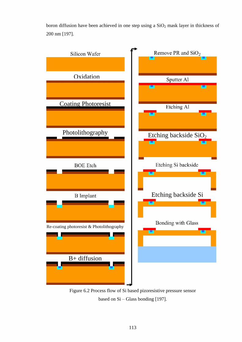
113
boron diffusion have been achieved in one step using a SiO2 mask layer in thickness of
200 nm [197].
Figure 6.2 Process flow of Si based pizoresistive pressure sensor
based on Si – Glass bonding [197].
Oxidation
Coating Photoresist
Photolithography
Re-coating photoresist & Photolithography
B+ diffusion
2
Etching backside SiO2
E
Etching backside Si
E

114
Figure 6.3 Optimised process flow of boron implantation [197].
To create piezoresistive sensing structures using the optimised implantation process,
AZ6112 photoresist was first spin coated onto the wafer after oxidation. During the UV
photolithography process, the wafer was soft baked at 90oC for 120 seconds and hard
baked at 120oC for 120 seconds. The energy for the boron ion implantation was 60 keV,
which formed the sensing piezoresistive layer with doping concentration of
7.5×10¹⁴
/cm3. An Ohmic contact layer containing larger doping concentration of about
Remove PR
Coat PR and photo
Etch SiO2
Remove PR and etch silicon
Etch SiO2
Bonding with Glass
Sputter Al
Oxidization
Silicon Wafer
Coat PR and photo
B Implant
Remove PR
Coat PR and photo
Etch SiO2
Remove PR and etch silicon
Coat PR and photo
Etch Al and remove PR
Oxidation
Photolithography
Photolithography
Etching SiO2
Etching SiO2

115
1019
/cm3 was also formed at the interface underneath the 200 nm thick SiO2 mask layer.
After ion implantation, an annealing process was carried out at temperature of 950 oC in
a dry nitrogen environment for 40 minutes [197]. The pressure sensors were provided
by Shanghai Institute of Microsystem and Information Technology (SIMIT), China.
Figure 6.4 Top view of the fabricated prototype piezoresistive pressure sensor.
Figure 6.5 Schematic layout of the contact pads.
The top view picture of the fabricated prototype piezoresistive pressure sensor is shown
in Fig. 6.4. The area of the full sensor was about 1 mm × 1 mm. 4 piezoresistors have

116
been fabricated to make up each device in the Wheatstone bridge. A schematic layout of
the contact pads is shown in Fig. 6.5. The dimensions of the contact pads were about 0.3
mm × 0.105 mm, and the thickness of the aluminium contact pads was between 300 and
400 nm. Using a 5 V DC power supply to provide the input current, pressure changes
result in a change in the sensor output voltage of the order of mV. As shown in Fig. 6.6,
a standard wire bonding process was used to electrically connect the positive input (Pad
1), positive output (Pad 2), negative input (Pads 3 and 4), and negative output (Pad 5).
(a)
(b)
Figure 6.6 (a) Schematic layout and (b) photo of wire bonded pressure sensor.
Al
pads
Al
pads

117
6.2 Design of Integrated Multi-Sensors
There is a growing interest in integrating health monitoring functions for advanced
electronic systems in order to make a timely decision for system repair or replacement
in safety critical applications. Microsystem health monitoring can improve the cost-
effectiveness of inspection and maintenance of the systems. With increasing
miniaturization and heterogeneous integration of electronic systems enabled by the
system-in-package (SiP) technology [47-49], it is becoming difficult to conduct
electrical tests using the conventional methods because of limited access to the electrical
contacts in stacked packages. Therefore it is necessary to use intelligent health
monitoring approaches to determine the status of such systems. Health monitoring
methods have already been developed for large systems and large structures, such as
aircraft and aerospace vehicles [53-57]. For health monitoring in compact or
miniaturized electronic systems, integrated sensors are essential. Fig. 6.7 shows a
schematic illustration of an electronic system with integrated sensors for health
monitoring. In this case an IC chip and a MEMS chip are integrated on a chip carrier.
The health monitoring sensors are integrated with the MEMS chip. For 3-D systems, the
microsystem health monitoring sensors or chips can be embedded in the system in
package (SiP) structures.
Figure 6.7 Schematic illustration of a microsystem with a health monitoring chip
attached [198].
Integration methods have been used to develop microsystem health monitoring
applications in advanced electronic systems. For health monitoring in electronic
systems, it is necessary to monitor multiple parameters inside a package in order to
assess the condition of a microsystem under operation. It is also necessary to monitor
the environmental parameters within a microsystem package such as temperature,
humidity and pressure. Two sensors single chip integration approaches have been
developed. Fig. 6.8 (a) shows a schematic layout of integrated sensors on a LiNbO3
substrate. In this case metal thin film based temperature sensors and SAW based
humidity sensors are fabricated on the substrate. A micromachined piezoresistive

118
pressure sensor is also assembled onto the same chip in order to obtain three integrated
sensors on the same substrate. The alternative approach has all of these 3 sensors on a
silicon substrate as illustrated in Fig. 6.8 (b). The temperature sensors are fabricated
either using a sputtered platinum thin film or using an electron beam evaporated nickel
thin film on the substrates. The pressure sensor is produced using the bulk silicon
micromachining techniques. The SAW based humidity sensor is fabricated on a
piezoelectric thin film such as ZnO or AlN that can be deposited on the silicon substrate
by sputtering.
(a)
(b)
Figure 6.8 Designs of integrated multi-sensors for embedded health monitoring based
on (a) piezoelectric substrate (such as LiNbO3) and (b) silicon substrate.
6.3 Fabrication Process of Integrated Multi-Sensors
6.3.1 Design for Integrated Sensors on LiNbO3 Substrate
The fabrication process flow of LiNbO3 based integrated multi-sensors is shown in Fig.
6.9. The platinum thin film temperature sensor is first fabricated by sputtering Pt film of
thickness between tens and hundreds of nanometres, which is then patterned into

119
meander structures using UV photolithography and ion beam etching. The IDTs of the
SAW humidity sensor and the contact pads of the pressure sensor can be achieved
together in the same process by sputtering an aluminium layer, which is patterned by
wet etching. The platinum patterns are able to survive in the aluminium etchant as they
remain on the substrate even after the aluminium etch. The BCB moisture capture film
of the humidity sensor is fabricated by spin coating and UV photolithography
processing. The sensor simply consists of the patterned BCB polymer. The silicon based
pre-fabricated piezoresistive pressure sensor would be assembled onto the substrate by
hybrid integration with cured glue. Wire bonding process is then used to provide the
interconnections between the bond pads on the sensor and bond lines on the substrate.
Figure 6.9 Fabrication processes of integrated multi-sensors on LiNbO3 substrate.
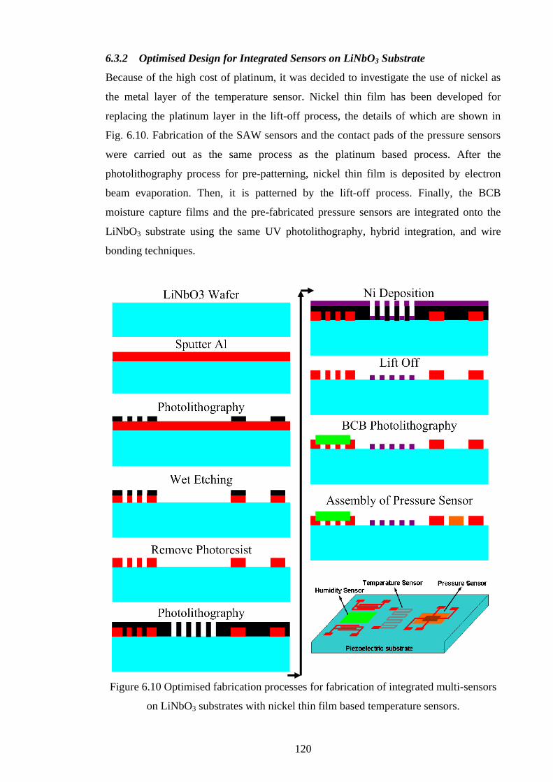
120
6.3.2 Optimised Design for Integrated Sensors on LiNbO3 Substrate
Because of the high cost of platinum, it was decided to investigate the use of nickel as
the metal layer of the temperature sensor. Nickel thin film has been developed for
replacing the platinum layer in the lift-off process, the details of which are shown in
Fig. 6.10. Fabrication of the SAW sensors and the contact pads of the pressure sensors
were carried out as the same process as the platinum based process. After the
photolithography process for pre-patterning, nickel thin film is deposited by electron
beam evaporation. Then, it is patterned by the lift-off process. Finally, the BCB
moisture capture films and the pre-fabricated pressure sensors are integrated onto the
LiNbO3 substrate using the same UV photolithography, hybrid integration, and wire
bonding techniques.
Figure 6.10 Optimised fabrication processes for fabrication of integrated multi-sensors
on LiNbO3 substrates with nickel thin film based temperature sensors.

121
6.3.3 Design for Integrated Sensors on Silicon Substrate
The temperature, humidity and pressure sensors have also been designed to be
fabricated on a silicon substrate. In this process, piezoelectric film is deposited on the
silicon substrate to act as the piezoelectric material in the fabrication of SAW based
humidity sensors. The details of the fabrication processes are shown in Fig. 6.11. Both
the sensors and the integration methods are suitable for applications in heath monitoring
in microsystems.
Figure 6.11 Process design of integrated multi-sensors on silicon substrate.

122
6.4 Fabrication of Integrated Multi-sensors
Based on fabrication capabilities, the LiNbO3 based integration process with platinum
thin film temperature sensors, shown in Fig. 6.9, has been carried out to fabricate the
integrated multi-sensors. Two 5-inch photomasks were designed for fabrication on the
integrated sensors on a LiNbO3 substrate (100mm diameter). The green patterns in Fig.
6.12 represent the Pt film based temperature sensors, and the red patterns are the Al
structures for both the IDT of the SAW humidity sensors and the contact pads of the
piezoresistive pressure sensors. The widths of Pt meander structures of the temperature
sensors were designed as 3, 5, and 10 m. The widths of the IDTs of the SAW humidity
sensors were designed as 4, 8, and 16 m. A picture of the integrated multi-sensors is
shown in Fig. 6.13. The structures for monitoring the pressure sensors and SAW
humidity sensors response to temperature change were also included in these mask
designs (shown in Fig. 6.14).
Figure 6.12 Design of photomasks for the integrated multi-sensors.

123
Figure 6.13 Layout of the integrated multi-sensors.
(a)
(b)
Figure 6.14 Layout of the designs for monitoring (a) the pressure sensor and (b) the
SAW humidity sensor responses versus temperature change.

124
Using the fabrication process outlined in Fig. 6.9, a titanium intermediate layer was first
sputtered using a Denton Vacuum Deposition System at power of 300 W for 120
seconds resulting in a film having a thickness of 30 nm. Then, the platinum temperature
sensing layer was sputtered with the same deposition system at power of 200 W for 300
seconds resulting in a film in thickness of 100 nm. During both sputtering processes, the
temperature of LiNbO3 substrate was kept constant at 25oC. The AZ6112 photoresist
was spin coated and patterned using UV photolithography. Fig. 6.15 shows a picture of
meander patterns in AZ6112 photoresist after the photolithography process. Using the
photoresist mask pattern, the platinum film was etched using an ion-beam etching
method with an IonFab 300 Plus (Oxford Instruments) at a power of 300 W for 70
seconds. Fig. 6.16 shows a picture of meander platinum patterns after the ion-beam
etching process and after removing the photoresist.
Figure 6.15 Picture of AZ6112 photoresist patterns on platinum film before the ion-
beam etching process.
Figure 6.16 Picture of platinum patterns after the ion-beam etching process.

125
After fabrication of the platinum thin film based temperature sensors, the SAW sensors
and the Al contact pads of the pressure sensors were fabricated by deposition of
aluminium using a Varian 3180 Sputtering System. This 300 nm thick aluminium layer
was subsequently patterned using a wet etching method.
Due to an error during the fabrication process, the SAW device of the integrated sensors
was short-circuited and was unable to function. The platinum thin film based
temperature sensors have already been successfully fabricated on LiNbO3 substrate and
the process design has been now established. So, the fabrication process of LiNbO3
based integrated sensors with nickel thin film temperature sensors (shown in Fig. 6.10)
was thus selected to obtain integrated sensors by considering the fabrication cost.
Instead of the combined platinum sputtering and wet etching processes, the lift-off
process for patterning electron beam evaporated nickel thin films was developed. By
using the negative photoresist, the same photomasks in Fig. 6.12 have been used for the
design of fabrication process shown in Fig. 6.10. Negative photoresist, AZ5214, was
spin coated on after the Al patterning for forming SAW devices and contact pads for
piezoresistive pressure sensors. The process steps for fabrication of the Ni temperature
sensors are shown in Fig. 6.17 ((a) to (c) for 5 m meander structures and (d) to (f) for
10 m meander structures. Fig. 6.17 (a) and (d) show the pictures of negative
photoresist patterned by UV photolithography before the Ni deposition. Fig. 6.17 (b)
and (e) show the pictures after Ni thin film deposition by electron beam evaporation.
Fig. 6.17 (c) and (f) show the pictures after the Ni lift off process.
After fabrication of both aluminium and nickel layers, the BCB moisture sensing films
were patterned, and the pre-fabricated piezoresistive pressure sensor was hybrid
integrated onto the LiNbO3 substrate using a cured glue (PERMABOND 820
Cyanoacrylate, Permabond Engineering Adhesives Ltd. UK). The electrical contacts
were then completed using the standard wire bonding process. The integrated multi-
sensors, shown in Fig. 6.18, were successfully fabricated with a footprint of 13 mm × 12
mm, based on the optimised fabrication processes shown in Fig. 6.10.

126
(a) (b) (c)
(d) (e) (f)
Figure 6.17 Picture of Ni meander structures with width of 5 m (a) patterned negative
photoresist, (b) e-beam evaporated Ni film, (c) fabricated Ni temperature sensor after
the lift off; and picture of Ni meander structures with width of 10 m (d) patterned
negative photoresist, (e) e-beam evaporated Ni film, (f) fabricated Ni temperature
sensor after the lift off.
Figure 6.18 Fabricated integrated multi-sensors.
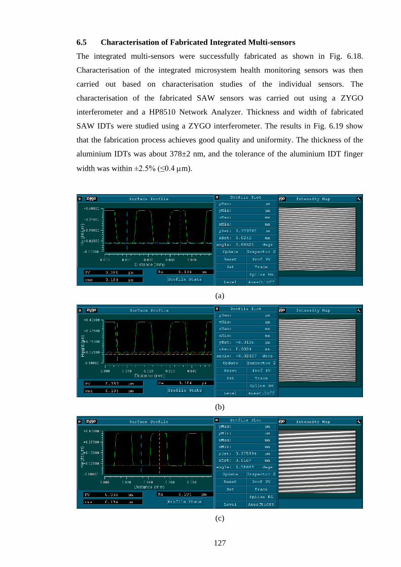
127
6.5 Characterisation of Fabricated Integrated Multi-sensors
The integrated multi-sensors were successfully fabricated as shown in Fig. 6.18.
Characterisation of the integrated microsystem health monitoring sensors was then
carried out based on characterisation studies of the individual sensors. The
characterisation of the fabricated SAW sensors was carried out using a ZYGO
interferometer and a HP8510 Network Analyzer. Thickness and width of fabricated
SAW IDTs were studied using a ZYGO interferometer. The results in Fig. 6.19 show
that the fabrication process achieves good quality and uniformity. The thickness of the
aluminium IDTs was about 378±2 nm, and the tolerance of the aluminium IDT finger
width was within ±2.5% (≤0.4 m).
(a)
(b)
(c)

128
(d)
Figure 6.19 Designed IDT-8 m with fabricated Al layer of (a) thickness 380 nm, (b)
width 8.1 m; and designed IDT-16 m with fabricated Al layer of (a) thickness 376
nm, (d) width 15.6 m.
Using a patterned BCB film, SAW based humidity sensors were characterised using
HP8510 Network Analyzer with previously designed test clips connections, and the
results at room humidity level are shown in Fig. 6.20. The resonance frequency of this 8
m IDT width SAW device was recorded at 125.15 MHz and the amplitude was
measured at -29.76 dB. More important for the sensing application, all the noise signals
of the operating device were below -50 dB. The fabricated BCB film based SAW device
on the chip of integrated multi-sensors is suitable for the humidity monitoring
applications using the reflection signals.
Figure 6.20 Reflection sensing signal of fabricated SAW humidity sensors (IDT widths
of 8 m).

129
The nickel thin film temperature sensors, with meander structure of widths of 5 and 10
m, have also been fabricated successfully for the integrated multi-sensors, using a lift
off process (shown in Fig. 6.17 (c) and (f)). Characterisation of the nickel thin film
sensors was carried out using a ZYGO interferometer. Test results on these sensors
show that the nickel thin film of thickness 18.6 nm was successfully obtained (shown in
Fig. 6.21 (a)), and tolerance of the fabricated meander track widths was less than ±1%.
This nickel thin film temperature sensing thermoresistor was then characterised using a
multimeter, and a resistance of about 13.77 k was recorded (shown in Fig. 6.22). The
nickel thin film based temperature sensors on the chip of integrated multi-sensors are
suitable for the temperature monitoring applications based on their physical
characteristics as thermistors.
(a)
(b)
Figure 6.21 Test results of ZYGO interferometer shows (a) the thickness of nickel film
was about 18.6 nm and (b) the designed 10 m meander structures were fabricated with
width of about 10.2 m.

130
Figure 6.22 Resistance of Ni thin film temperature sensor on the chip of integrated
sensors being measured with the multimeter.
Figure 6.23 Wire bonded piezoresistive pressure sensor integrated on the multi-sensor
chip by hybrid integration.

131
The piezoresistive pressure sensors were successfully assembled using a commercial
glue (PERMABOND 820 Cyanoacrylate, Permabond Engineering Adhesives Ltd. UK)
and electrically connected using the standard wire bonding process. Fig. 6.23 shows that
the gold wire contacts were successfully obtained and the piezoresistive pressure
sensors are suitable for this hybrid integration process for achieving the integrated
microsystem health monitoring sensor applications.
6.6 Temperature Monitoring Chip
Temperature monitoring chips have also been designed and fabricated successfully. The
photomasks designs have been shown in Fig. 6.14 (a) and (b). These temperature
monitoring chips could be used for self monitoring and automatic correction of
piezoresistive pressure sensors, accelerometers, and all other kinds of temperature
sensitive microsensors and microsystems. A picture of a fabricated temperature
monitoring chip attached with a piezoresistive pressure sensor is shown in Fig. 6.24,
which includes two temperature sensors located at the left and right edges of the
pressure sensor. A picture of a SAW based temperature monitoring chip is shown in
Fig. 6.25, which can be used for real time temperature monitoring and self correction
for SAW based resonators, sensors, and filters.
Figure 6.24 Pressure sensor attached on a fabricated temperature monitoring chip.

132
Figure 6.25 Fabricated temperature monitoring chip for SAW devices.
6.7 Summary
A highly boron doped silicon layer was selected for making peizoresistors into
piezoresistive pressure sensors. The sensors consist of a vacuum or constant pressure
sealed cavity, monitored using a Wheatstone bridge in a DC test circuit. An optimised
process for boron implantation has been used for producing pre-fabricated piezoresistive
pressure sensors supplied by a research partner. Using a SiO2 resistant layer of thickness
200 nm to mask the wafer during the ion implant, both the boron implantation and the
high concentration boron diffusion could be achieved in one process step.
For applications in heath monitoring in miniature electronic systems, fabrication
processes of integrated multi-sensors were designed based on both LiNbO3 and silicon
substrates. By considering the fabrication cost, the nickel thin film based fabrication has
been further developed and optimised using LiNbO3 substrates. Both the sensor
structures and the fabrication processes were studied in detail. Fabrication of integrated
multi-sensors based on LiNbO3 substrate has been investigated. Two 5-inch photomasks
were designed for fabricating the integrated multi-sensors on 100 mm diameter LiNbO3
substrates. Both IDTs of SAW devices and the contact pads of pressure sensors were
fabricated using sputtered Al film, which was patterned using a wet etching method.
The temperature sensor was produced using electron beam evaporated Ni thin film,
which was patterned using a lift off process. A piezoresistive pressure sensor was
hybrid integrated using cured glue and electrically connected using the standard wire
bonding process. Successfully fabricated integrated multi-sensors, in a footprint of 13
mm × 12 mm, were characterised using the ZYGO interferometer, HP8510 Network
Analyzer, multimeter and microscope. In the integrated multi-sensors, the SAW

133
humidity sensor was obtained with IDT of thickness of 378±2 nm and different IDTs
widths of 8 and 16 m with a tolerance of about ±2.5%. The resonance frequency of the
8 m IDT width SAW device was recorded as 125.15 MHz and amplitude was
measured at -29.76 dB, while all the noise signals were below -50 dB. The nickel thin
film temperature sensor was successfully fabricated with meander structure widths of 5
and 10 m. Fabricated nickel thin film was 18.6 nm thick and tolerance of track widths
was less than ±1%, resulting a resistance of 13.77 kwith a meander line width of 10
m. The integrated piezoresistive pressure sensor was observed using a microscope and
was shown to have good electrical interconnects.
A temperature monitoring chip has also been considered and fabricated, and these are
suitable for self monitoring of temperature. Also the operating tolerance allows for the
automatic correction of temperature sensitive microsensors and microsystems, such as
piezoresistive pressure sensors and accelerometers. The work has successfully
demonstrated the flexibility of integration of multi-sensors for microsystem health
monitoring applications.

134
Chapter 7 Conclusions and Future Work
7.1 Conclusions
Simulation, fabrication, integration and characterisation of high sensitivity, miniature
temperature and humidity sensors has been investigated in this PhD thesis. Platinum
thin film temperature sensor arrays have been successfully used for embedded real time
monitoring of a laser assisted polymer bonding process. The structure designs, process
flows and fabrication of integrated multi-sensors for embedded health monitoring of
microsystems have also been investigated in detail. Using an optimised fabrication
process and hybrid method, integrated multi-sensors have been successfully fabricated
on a LiNbO3 substrate with a footprint of 13 mm × 12 mm with multi monitoring
functions for temperature, humidity and pressure.
Based on the theoretical analysis and FEM simulations, the metal thin film temperature
sensors have been designed in meander structures with track widths of 3, 5, 7 and 10
m. The footprint of the thin film temperature sensor with a 3m track width was just
240 m × 250 m. Deposited by sputtering and patterned by ion-beam etching process,
the platinum based temperature sensors have been fabricated and allow a good linear
response. Nickel based sensors have also been fabricated successfully using electron
beam evaporation and wet etching methods. The nickel based sensor with 5 m of track
width had a sensitivity of 32.25mV/K at a constant current of 0.1mA. An annealing
process was subsequently used to stabilise the Ni thin film sensor. After the annealing
process, the corresponding temperature coefficients of resistance (TCR) of the platinum
based sensors were determined to be from 1.78×10⁻³
/°C to 2.26×10⁻³
/°C at 20°C.
An experimental study of accurate temperature monitoring in a laser assisted BCB
polymer bonding process for MEMS packaging was carried out using an embedded thin
film microsensor array. Beam forming optical elements were used to generate top-hat
and frame-shaped beam profiles. The results showed that the amplitude and
characteristic of the laser generated temperature change not only depends on the laser
power but also depends on the package assembly to be bonded and the configuration of
materials in the bonding setup. Three kinds of package assemblies were studied,
including silicon cap to glass substrate, glass cap to silicon substrate and silicon cap to
silicon substrate. Using a frame-shaped beam, the temperature at the centre of the

135
bottom substrate was obtained as ~50ºC lower compared to that obtained using a top-hat
beam. The reduction of temperature at the centre device packaging area is highly
beneficial for MEMS packaging of temperature sensitive devices. Using a single
exponential function to describe the temperatures characteristics, results show that the
thermal constants of package assemblies are largely independent of the beam profiles
but highly dependent on the thermal arrangement of the materials underneath the bottom
substrate.
Utilizing the moisture capture capabilities of BCB films, SAW based humidity sensors
have been designed and fabricated on 128° cut lithium niobate piezoelectric substrates.
The sensors use IDTs with widths of 4, 8 and 16 m. Measured using a HP8510
Network Analyzer, the resonance frequencies of the fabricated SAW sensors were
248.60, 124.82, and 61.20 MHz, respectively. These are in good agreement with the
theoretical values of 249.50, 124.75, and 62.19 MHz (with SAW velocity of 3992 m/s
for 128° cut LiNbO3 substrates). Two test configurations, using silver loaded epoxy and
using test clips, were developed using two types of metal contact connections. There
was a negligible difference between results of measurement using the two different
connection configurations. Test results on SAW sensor show that the chemically
reduced lithium niobate substrates had the same piezoelectric properties as regular
lithium niobate substrates. The measured Q factor of a SAW sensor with IDT width of 8
m was increased 27.4%, from 581 to 740 by the application of the reflection grating
structures. The temperature change resulted in shift of the SAW resonance frequency by
4.26 kHz/°C, around 34 ppm change in the resonance frequency of 124.82 MHz. Based
on the reflection signals of the BCB based SAW humidity sensors, a sensitivity of 0.26
dB/RH% was achieved under controlled humidity level between 8.6% and 90.6% RH.
After the design, fabrication and testing of the metal thin film based temperature sensors
and the BCB films based SAW humidity sensors, the structure designs and the
fabrication processes were performed on both LiNbO3 and ZnO/Si substrates for
applications in heath monitoring of miniature electronic systems. Prototype
piezoresistive pressure sensors operating at different ranges of 0 to 1.5 bar and 0 to 7
bar were selected for the hybrid integration on a single chip with the temperature and
humidity sensors. Two 5-inch photomasks were designed for fabricating the integrated
multi-sensors on the LiNbO3 substrates. The widths of metal thin film meander
structures of the temperature sensors were designed as 3, 5, and 10 m. The widths of

136
the IDTs of the SAW humidity sensors were designed as 4, 8, and 16 m. The
aluminium structures for both the IDT of the SAW humidity sensors and the contact
pads of the piezoresistive pressure sensors were fabricated with just one process step.
This saves one photomask as well as the cost of UV photolithography process time.
Using an optimised fabrication process, the integrated multi-sensors were successfully
fabricated on a LiNbO3 substrate with a footprint of 13 mm × 12 mm with multi
monitoring functions for temperature, humidity and pressure sensing applications.
7.2 Future work
In the work described in this thesis, high sensitivity miniature temperature, humidity
and pressure sensors have been successfully integrated on a single substrate. The
sensors have the potential to be used for not only the health monitoring of Microsystems
but also for intelligent process controls and embedded conditional monitoring
applications. In hybrid integration and SiP technologies, integrated multi-sensors can
meet the challenges of test and reliability validation. This provides low-cost integration
of functions for self-testing of system interconnects. Key parameters can be monitored
in mission mode and a level of fault tolerance/self-repair can be achieved.
After successful fabrication and characterisation, the integrated multi-sensors could be
used for other applications such as intelligent process control and embedded conditional
monitoring. By further studying of the long term stability, packaging technology would
be properly considered for sensor protection, especially for the BCB based SAW
humidity sensors, which will lead to the enhancements of both sensitivity and the
reliability of the operating sensors. A reduction of SAW reflection amplitude and
sensor’s sensitivity was observed after 41 days of the initial test (shown in Fig. 7.1).
This may be because the BCB sensing film was contaminated since the unpackaged
sensor was operated outside the cleanroom environment. Meanwhile, the linear
relationship between the relative humidity level and the amplitude of the SAW
reflection signals could be interesting to be studied and discussed in theoretical details.
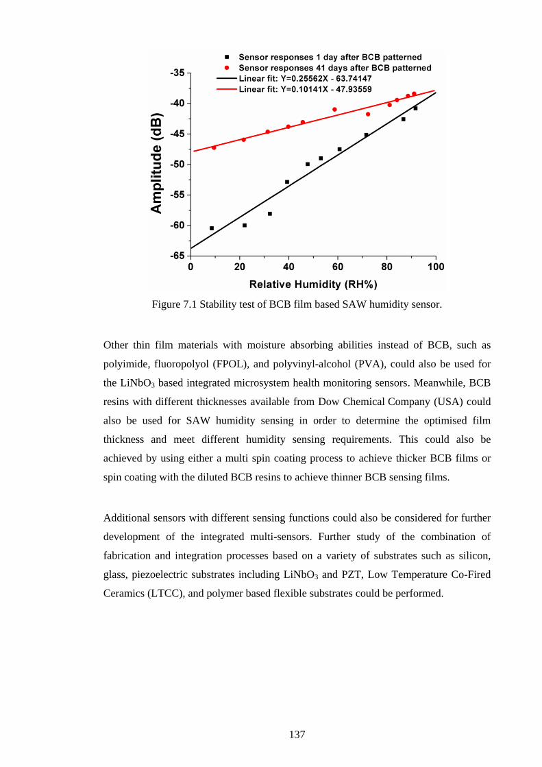
137
Figure 7.1 Stability test of BCB film based SAW humidity sensor.
Other thin film materials with moisture absorbing abilities instead of BCB, such as
polyimide, fluoropolyol (FPOL), and polyvinyl-alcohol (PVA), could also be used for
the LiNbO3 based integrated microsystem health monitoring sensors. Meanwhile, BCB
resins with different thicknesses available from Dow Chemical Company (USA) could
also be used for SAW humidity sensing in order to determine the optimised film
thickness and meet different humidity sensing requirements. This could also be
achieved by using either a multi spin coating process to achieve thicker BCB films or
spin coating with the diluted BCB resins to achieve thinner BCB sensing films.
Additional sensors with different sensing functions could also be considered for further
development of the integrated multi-sensors. Further study of the combination of
fabrication and integration processes based on a variety of substrates such as silicon,
glass, piezoelectric substrates including LiNbO3 and PZT, Low Temperature Co-Fired
Ceramics (LTCC), and polymer based flexible substrates could be performed.

138
References
[1] M.X. Sham, Y.C. Chen, L.W Leung, et al., “Challenges and Opportunities in
System-in-Package (SiP) Business”, 7th International Conference on Electronic
Packaging Technology (ICEPT '06), 26-29 Aug. 2006 Page(s):1–5.
[2] V. Garg, S. Lacy, D.E. Schimmel, et al., “Incorporating multi-chip module
packaging constraints into system design”, Proceedings of European Design and
Test Conference, 1996 (ED&TC 96), 11-14 March 1996 Page(s):508–513.
[3] System in a Package (SIP), www.SiliconFarEast.com.
[4] Rao Tummala, “SoC vs. MCM vs SiP vs. SoP”, Advanced Packaging,
ap.pennnet.com, July, 2006.
[5] Seunghee Park, Chung-Bang Yun and Daniel J. Inman, “A Self-contained
Active Sensor System for Health Monitoring of Civil Infrastructures”, 5th IEEE
Conference on Sensors, 2006, Oct. 2006 Page(s):798–802.
[6] Yan Yu and Jinping Ou, “Design of wireless intelligent sensor for structural
health monitoring”, Proceedings of Intelligent Sensors, Sensor Networks and
Information Processing Conference, 2004, 14-17 Dec. 2004 Page(s):1–5.
[7] B. Nickerson and R. Lally, “Development of a smart wireless networkable
sensor for aircraft engine health management”, IEEE Proceedings of Aerospace
Conference, 2001, Volume 7, 10-17 March 2001 Page(s):3255–3262.
[8] S. George, “Development of a vibration-powered wireless temperature sensor
and accelerometer for health monitoring”, IEEE Proceedings of Aerospace
Conference, 2006, 4-11 March 2006 Page(s):1-8.
[9] S.A. Lewis and T.G. Edwards, “Smart sensors and system health management
tools for avionics and mechanical systems”, Digital Avionics Systems
Conference, 1997. 16th
DASC., AIAA/IEEE Volume 2, 26-30 Oct. 1997
Page(s):8.5(1)-8.5(7).
[10] J. Bryzek, “Impact of MEMS technology on society”, Sensors and Actuators A,
Vol 56, 1996 Page(s):1-9.
[11] K. Gilleo, “MEMS challenge: can this technology catch the internet lightwave”,
IMECE 2000 MEMS Symposium, Orlando, Nov 5-10, 2000 Page(s):615-622.
139
[12] http://www.zyvex.com/nanotech/feynman.html (Date: 30/10/2010)
[13] http://www.same-
conference.org/same_2003/images/documents/tutorials/Tutorial_3_MEMS_P1
(Date: 30/10/2010)
[14] http://www.aero.org/publications/helvajian/helvajian-1.html (Date: 30/10/2010)
[15] http://robotics.eecs.berkeley.edu/~pister/245/Notes/Intro.pdf (Date: 30/10/2010)
[16] M. Abraham, W. Ehrfeld, V. Hessel et al., “Microsystem Technology: Between
Research and Industrial Application”, Microelectronic Engineering, Volumes
41-42, March 1998, Page(s): 47-52.
[17] S. Wu , Q. Lin , Y. Yuen, et al., “MEMS flow sensors for nanofluidic
applications”, IEEE Proc of 13th Annual International Conference on MEMS,
Miyazaki(Japan), 23-27 Jan 2000 page(s): 745-750.
[18] Khalil Najafi, “Smart Sensors”, J. Micromech. Microeng, 1(1991) page(s): 86-
102.
[19] Elena Gaura and Robert Newman, Smart Mems and Sensor Systems, illustrated
edition, Imperial College Press, Sep 2006.
[20] Liao CanXing, Li Xingshan, Zhang Ping, and Dai Jing, A Review on Optimal
Sensor Placement for Health Monitoring, 8th International Conference on
Electronic Measurement and Instruments (ICEMI) 2007, Page(s): 4-170 - 4-173.
[21] T. Becker, M. Kluge, J. Schalk, K. Tiplady, C. Paget, U. Hilleringmann, T.
Otterpohl, Autonomous Sensor Nodes for Aircraft Structural Health Monitoring,
IEEE Sensors Journal, Volume: 9 , Issue: 11, 2009, Page(s): 1589 - 1595.
[22] R.K. Draney, High Temperature Sensor for Bearing Health Monitoring, 2008
IEEE Aerospace Conference, Page(s): 1 - 7.
[23] A. Zalt, V. Meganathan, S. Yehia, O. Abudayyeh, and I. Abdel-Qader,
Evaluating sensors for bridge health monitoring, 2007 IEEE International
Conference on Electro/Information Technology, Page(s): 368 - 372.
[24] S. Fatikow and U. Rembold, Microsystems Technology and Micro-robotics,
Springer-Verlag, Berlin, 1997.
[25] D. Qu and S. Gao, “Researches on Microelectromechanical Systems and Its

140
Applications”, SCIENCE & TECHNOLOGY REVIEW, No.4 (204) page(s):17-
21.
[26] J.M. Bustillo, R.T. Howe and R.S. Muller, “Surface micromachining for
microelectromechanical systems”, Proceedings of the IEEE, Volume 86, Issue 8,
Aug. 1998 Page(s):1552–1574.
[27] http://www.aero.org/publications/helvajian/helvajian-2.html (Date: 30/10/2010)
[28] G.T.A. Kovacs, N.I. Maluf and K.E. Petersen, “Bulk micromachining of
silicon”, Proceedings of the IEEE, Volume 86, Issue 8, Aug. 1998
Page(s):1536-1551.
[29] M. Esashi, “Microsystems by Bulk Micromachining”, 30th European
Microwave Conference, Oct. 2000 Page(s):1-4.
[30] M. Esashi, Y. Haga, “Silicon bulk micromachining”, 1st Annual International
Conference On Microtechnologies in Medicine and Biology, 12-14 Oct. 2000
Page(s):7-12.
[31] http://www.suss.com/applications/wafer_bonding/ (Date: 30/10/2010)
[32] Laura Peters, “Wafer Bonding Enables New Technologies and Applications”,
http://www.semiconductor.net/article/CA331034.html (Date: 30/10/2010)
[33] M.A. Schmidt, “Wafer-to-wafer bonding for microstructure formation”,
Proceedings of the IEEE, Volume 86, Issue 8, Aug. 1998 Page(s):1575–1585.
[34] Z.H. Zhu, F.E. Ejeckam, Y. Qian, etc.., “Wafer bonding technology and its
applications in optoelectronic devices and materials”, IEEE Journal of Quantum
Electronics, Volume 3, Issue 3, June 1997 Page(s):927-936.
[35] http://www.freepatentsonline.com/4170472.html (Date: 30/10/2010)
[36] V.L. Spiering, J.W. Berenschot, M. Elwenspoek, etc.., “Sacrificial wafer
bonding for planarization after very deep etching”, Journal of
Microelectromechanical Systems, Volume 4, Issue 3, Sept. 1995 Page(s):151-
157.
[37] Z. Tong, “MEMS Technology and Process Equipments”, Equipment for
Electronic Products Marufacturing, Vol33, No.1, 2004, page(s):5-11.
[38] Wannok Sio, “MEMS (Microelectromechanical System)”, Oct. 2002,

141
http://www.engr.ku.edu/~rhale/ae510/websites_f02/mems.pdf
(Date: 30/10/2010)
[39] Salvatore A. Vittorio, “Review Article: MicroElectroMechanical Systems
(MEMS)”, Oct. 2001, http://www.csa.com/discoveryguides/mems/overview.php
(Date: 30/10/2010)
[40] J.A. Walraven, “Introduction to applications and industries for
microelectromechanical systems (MEMS)”, Test Conference, 2003.
Proceedings. ITC 2003. International, Volume 1, Sept. 30-Oct. 2, 2003
Page(s):674–680.
[41] http://www.answers.com/topic/multi-chip-module (Date: 30/10/2010)
[42] http://www.eleceng.adelaide.edu.au/Personal/alsarawi/node12.html
(Date: 30/10/2010)
[43] http://www.cmac.com/dms/services/manufacture/packaging/MCMs.php
(Date: 30/10/2010)
[44] Toshio Sudo, “Present and Future Directions for Multichip Module
Technologies”, VLSI Circuits, 1994. Digest of Technical Papers, 1994
Symposium on JUNE 9-11, 1994 Page(s):51–54.
[45] R.H. Bruce,W.P. Meuli and Ho Jackson, “Multi Chip Modules”, Design
Automation, 1989. 26th Conference on 25-29 June 1989, Page(s):389 – 393.
[46] V. Garg, S. Lacy, D.E. Schimmel, etc., “Incorporating multi-chip module
packaging constraints into system design”, European Design and Test
Conference, 1996. ED&TC 96. Proceedings, 11-14 March 1996 Page(s):508 –
513.
[47] Robert C. Pfahl, “System in Package Technology”, International Electronics
Manufacturing Initiative, 2005.
[48] Jani Miettinen, Matti Mantysalo, Kimmo Kaija, and Eero O. Ristolainen, System
Design Issues for 3D System-in-Package (Sip), Proceedings of 54th Electronic
Components and Technology Conference, 2004, Vol.1, Page(s): 610 - 615.
[49] J. Miettinen, M. Mantysalo, K. Kaija, etc., “System design issues for 3D system-
in-package (SiP)”, Electronic Components and Technology Conference, 2004.
Proceedings. Volume 1, 1-4 June 2004 Page(s):610–615.
142
[50] www.elecdesign.com, “Packaging Rides The Z Axis Into The Third Dimension”,
Penton Media, Inc.. (Date: 30/10/2010)
[51] http://www.eetimes.com/news/design/showArticle.jhtml?articleID=188701766&
pgno=1 (Date: 30/10/2010)
[52] Joseph Adam and Mark Bird, SiP Technology Offers Packaging Alternatives for
Design, Source: http://www.electroiq.com/index/display/packaging-article-
display/211535/articles/advanced-packaging/volume-13/issue-9/features/cover-
story/sip-technology-offers-packaging-alternatives-for-design.html
(Date: 30/10/2010)
[53] A. Mishra, F.M. Gondal, A.A. Afrashteh, etc., “Embedded wireless sensors for
aircraft/automobile tire structural health monitoring”, 2nd IEEE Workshop on
Wireless Mesh Networks (WiMesh), 2006 Page(s):163 – 165.
[54] G.B.Tait and R.S. Rogowski, “Fibre Bragg grating sensors for real-time health
monitoring of aerospace vehicles”, Quantum Electronics and Laser Science
Conference, 22-27 May 2005, Volume 2, Page(s):924 – 926.
[55] J.W. Borinski, S.A. Meller, W.J. Pulliam, etc., “Aircraft health monitoring using
optical fiber sensors”, Proceedings of Digital Avionics Systems Conferences
(DASC), 7-13 Oct. 2000. Volume 2, Page(s):6D1/1 - 6D1/8.
[56] B. Nickerson and R. Lally, “Development of a smart wireless networkable
sensor for aircraft engine health management”, Proceedings of IEEE Aerospace
Conference, 10-17 March 2001. Volume 7, Page(s):3255 – 3262.
[57] Seunghee Park, Chung-Bang Yun and Daniel J. Inman, “A Self-contained
Active Sensor System for Health Monitoring of Civil Infrastructures”, 5th IEEE
Conference on Sensors, Oct. 2006. Page(s):798 – 802.
[58] G. Konstantinidis, P.D. Wilcox and B.W.Drinkwater, “An Investigation Into the
Temperature Stability of a Guided Wave Structural Health Monitoring System
Using Permanently Attached Sensors”, Sensors Journal, IEEE. Volume 7, Issue
5, May 2007 Page(s):905 – 912.
[59] J.W. Borinski, C.D. Boyd, J.A. Dietz, etc., “Fiber optic sensors for predictive
health monitoring”, AUTOTESTCON Proceedings of IEEE Systems Readiness
Technology Conference, 20-23 Aug. 2001, Page(s):250 – 262.

143
[60] S.E. George. M. Bocko and G.W. Nickerson, “Evaluation of a vibration-
powered, wireless temperature sensor for health monitoring”, IEEE Aerospace
Conference 5-12 March 2005, Page(s):3775 – 3781.
[61] S. George, “Development of a vibration-powered wireless temperature sensor
and accelerometer for health monitoring”, IEEE Aerospace Conference 4-11
March 2006, Page(s):1 – 8.
[62] D. Nickles, D. Rauth, and J. Schmalzel, “Enhanced smart sensor for integrated
system health management”, IEEE Proceedings of Sensors Applications
Symposium 2006, Page(s):208 – 212.
[63] Hossain, “An intelligent sensor network system coupled with statistical process
model for predicting machinery health and failure”, Sensors for Industry
Conference, 2nd ISA/IEEE, 19-21 Nov. 2002, Page(s):52–56.
[64] S.A. Lewis and T.G. Edwards, “Smart sensors and system health management
tools for avionics and mechanical systems”, Digital Avionics Systems
Conference (DASC) AIAA/IEEE, 26-30 Oct. 1997, Volume 2, Page(s):8.5 - 1-
8.5-7.
[65] C.Y. Wong, and S.J. Hood, “Impact of process monitoring in semiconductor
manufacturing”, Proceedings of 16th IEEE/CPMT International Electronics
Manufacturing Technology (IEMT) Symposium, Vol. 1, Sep. 1994 Page(s):
221-225.
[66] C. Eaves-Walton, K. Hunt, and S. Redford, “Intelligent online process
monitoring and fault isolation”, IEE Colloquium on Condition Monitoring and
Failure Diagnosis - Part 1, Vol. 1, Nov. 1988, page(s): 6/1-6/4,.
[67] Lin, K.C.; Marcadal, C.; Ganguli, S.; Zheng, Bo; Schmitt, J. and Chen, Ling
“Characterization of copper CVD process by a process monitor”, IEEE/SEMI
Advanced Semiconductor Manufacturing Conference and Workshop, pp. 440-
445, Sept. 1999.
[68] Kojima, T.; Miyajima, M.; Akaboshi, F.; Yogo, T.; Ishimoto, S. and Okuda, A.
“Application of CMP process monitor to Cu polishing”, IEEE Transactions on
Semiconductor Manufacturing, Vol. 13, Issue 3, pp. 293-299, Aug. 2000.
[69] Brokelmann, M.; Wallaschek, J. and Hesse, H. “Bond process monitoring via
self-sensing piezoelectric transducers”, Proceedings of the IEEE International

144
Frequency Control Symposium and Exposition, pp. 125-129, Aug. 2004.
[70] Kalashnikov, A.N.; Ivchenko, V.; Challis, R.E. and Holmes, A.K.
“Compensation for temperature variation in ultrasonic chemical process
monitoring”, 2005 IEEE Ultrasonics Symposium, Vol. 2 pp. 1151-1154, Sept.
2005.
[71] Suman, S.; Gaitan, M.; Joshi, Y. and Harman, G.G. “Wire-bonding process
monitoring using thermopile temperature sensor”, IEEE Transactions on
Advanced Packaging, Vol. 28, Issue 4, pp. 685-693, Nov. 2005.
[72] Sopori, B.; Zhang, Yi; Chen, Wei and Madjdpour, J. “BSilicon solar cell process
monitoring by PV-reflectometer”, Conference Record of the 28th IEEE
Photovoltaic Specialists Conference, pp. 120-123, Sept. 2000.
[73] http://en.wikipedia.org/wiki/Temperature_measure (Date: 30/10/2010)
[74] http://en.wikipedia.org/wiki/Temperature_measure#Temperature_measurement
(Date: 30/10/2010)
[75] http://www.temperatures.com/ (Date: 30/10/2010)
[76] Peter Orrell, “how to measure temperature”, Sensor Review, Vol. 15 No. 4,
1995, Page(s):28 – 30.
[77] http://www.temperatures.com/tcs.html (Date: 30/10/2010)
[78] http://www.facstaff.bucknell.edu/mastascu/elessonshtml/Sensors/TempThermCp
l.html (Date: 30/10/2010)
[79] http://www.dbanks.demon.co.uk/ueng/thermsens.html (Date: 30/10/2010)
[80] J.J. Park and M. Taya, “Micro-temperature sensor array with thin-film
thermocouples”, Electronics Letters, Volume 40, Issue 10, 13 May 2004,
Page(s):599 – 601.
[81] K. Miyazaki, T. Takamiya and H. Tsukamoto, “Fabrication of micro-thin film
thermocouples”, International Conference on Thermoelectrics (ICT), 17-21 Aug.
2003, Page(s):673 – 676.
[82] http://www.kele.com/tech/monitor/temperature/TRefTem4.html
(Date: 30/10/2010)
[83] http://www.temperatures.com/rtds.html (Date: 30/10/2010)

145
[84] http://www.ussensor.com/technical_data.html (Date: 30/10/2010)
[85] T. Bernstein and Pao Ping Chang, “Calculation of Self-Heating Current for a
Resistance Wire Temperature Sensor”, IEEE Transactions on Industrial
Electronics and Control Instrumentation (IECI), Vol. 16, Issue 1, July 1969
Page(s):99 – 102.
[86] http://www.allaboutcircuits.com/vol_1/chpt_12/6.html (Date: 30/10/2010)
[87] http://www.nuist.edu.cn/wlsy/show.aspx?id=517&cid=29 (Date: 30/10/2010)
[88] Julian W. Gardner, Microsensors: principle and application, Bookcraft (bath)
Ltd. 1994, Great Britain. Chapter 5.
[89] http://hyperphysics.phy-astr.gsu.edu/hbase/Tables/rstiv.html (Date: 30/10/2010)
[90] http://www.lakeshore.com/temp/sen/prtd.html (Date: 30/10/2010)
[91] http://en.wikipedia.org/wiki/Infrared_thermometer (Date: 30/10/2010)
[92] M. Miiller, W. Budde, R. Gottfried-Gottfi-ied, etc., “A Thermoelectric Infrared
Radiation Sensor With Monolithically Integrated Amplifier Stage And
Temperature Sesnor”, The 8th International Conference on Solid-state Sensors
and Actuators, and Eurosensors IX. Stockholm, Sweden, 25-29, June 1995,
Page(s):640 – 643.
[93] K. Shinzato, J. Ishii, Y. Shimizu, etc., “High-speed Infrared Radiation
Thermometers for Measurement of Thermophysical Properties”, IEEE SICE
Osaka, Aug. 5-7.2002, Page(s):2077 – 2081.
[94] Wook Jae Yoo, Bongsoo Lee, Dong Hyun Cho, etc., “Infrared Radiation
Thermometer Using a Silver Halides Optical Fiber for Biomedical
Applications”, IEEE SENSORS 2006, EXCO, Daegu, Korea. 22-25 Oct. 2006,
Page(s):631-633.
[95] http://en.wikipedia.org/wiki/Optical_Fiber#Fiber_optic_sensors
(Date: 30/10/2010)
[96] Zhiyi Zhang, K. T. V. Grattan and A. W. Palmer, “Fiber optic temperature
sensor based on the cross referencing between blackbody radiation and
fluorescence lifetime”, Review of Scientific Instruments, May 1992, Vol. 63,
Issue 5, Page(s):3177-3181.

146
[97] Jonghan Park, Gabriele Bolognini, Duckey Lee, etc., “Raman-Based Distributed
Temperature Sensor With Simplex Coding and Link Optimization”, IEEE
PHOTONICS TECHNOLOGY LETTERS, VOL. 18, NO. 17, Sep. 2006,
Page(s):1879-1881.
[98] V. 3. Kados and G. J. Sonek, “A Dewpoint Temperature Sensor Based on Nd3+-
Doped Fiber Fluorescence”, IEEE PHOTONICS TECHNOLOGY LETTERS,
VOL. 7, NO. 10, Oct. 1995, Page(s):1198-1200.
[99] Alberto Álvarez-Herrero, H. Guerrero, T. Belenguer, etc., “High-Sensitivity
Temperature Sensor Based on Overlay on Side-Polished Fibers”, IEEE
PHOTONICS TECHNOLOGY LETTERS, VOL. 12, NO. 8, Aug. 2000,
Page(s):1043-1045.
[100] Javier Senosiain, Idoya Díaz, Ainhoa Gastón, etc., “High Sensitivity
Temperature Sensor Based on Side-Polished Optical Fiber”, IEEE
TRANSACTIONS ON INSTRUMENTATION AND MEASUREMENT, VOL.
50, NO. 6, DECEMBER 2001, Page(s):1656-1660.
[101] Pak Lim Chu and Danny Wong, “Phase Sensitivity of Polarization-Maintaining
Optical Fiber Used as Temperature Sensor”, JOURNAL OF LIGNTWAVE
TECHNOLOGY, VOL. LT-4. NO. I , JANUARY 1986, Page(s):41-49.
[102] C.F.R. Mateus and C.L. Barbosa, “Low Power, High Sensitivity Temperature
Sensor Using Fiber Bragg Gratings and VCSEL”, IEEE Lasers & Electro-Optics
Society, Oct. 2006 Page(s):354 – 355.
[103] Tyson L. Lowder, Kevin H. Smith, Benjamin L. Ipson, etc., “High-Temperature
Sensing Using Surface Relief Fiber Bragg Gratings”, IEEE PHOTONICS
TECHNOLOGY LETTERS, VOL. 17, NO. 9, Sep. 2005, Page(s):1926 – 1928.
[104] Bowei Zhang and Mojtaba Kahrizi, “High-Temperature Resistance Fiber Bragg
Grating Temperature Sensor Fabrication”, IEEE SENSORS JOURNAL, VOL.
7, NO. 4, Apr. 2007, Page(s):586– 591.
[105] Jian Ju, Zhi Wang, Wei Jin, etc., “Temperature Sensitivity of a Two-Mode
Photonic Crystal Fiber Interferometric Sensor”, IEEE PHOTONICS
TECHNOLOGY LETTERS, VOL. 18, NO. 20, Oct. 15, 2006, Page(s):2168–
2170.
[106] Hak-Rin Kim, Eunje Jang and Sin-Doo Lee, “Electrooptic Temperature Sensor

147
Based on a Fabry–Pérot Resonator With a Liquid Crystal Film”, IEEE
PHOTONICS TECHNOLOGY LETTERS, VOL. 18, NO. 8, APRIL 15, 2006,
Page(s): 905– 907.
[107] http://en.wikipedia.org/wiki/Diode (Date: 30/10/2010)
[108] http://www.vias.org/feee/sensor_temp_diode.html (Date: 30/10/2010)
[109] Raimundo Carlos Silverio Freire, SCrgio Daher, and Gurdip Singh Deep, A
Highly Linear Single p-n Junction Temperature Sensor, IEEE TRANSECTIONS
ON INSTRUMENTATION AND MEASUREMENT, VOL. 43, NO. 2, APRIL
1994, Page(s): 127-132.
[110] Yu. M. Shwarts, A. V. Kondrachuk, M. M. Shwarts, L. I. Spinar, and E. F.
Venger, The effect of heterojunction properties of the diode temperature sensors
on low temperature current transfer and temperature response curves, the third
international European conference on advanced semiconductor devices and
microsystems, Smolenice Castle, Slovakia, 16-18 Pct. 2000, Page(s): 453-456.
[111] S. Santra, P. K. Guha, S. Z. Ali, I. Haneef, F. Udrea, and J. W. Gardner, SOI
Diode Temperature Sensor Operated at Ultra High Temperatures – A Critical
Analysis, IEEE SENSORS Conference 2008, Page(s): 78-81.
[112] A. Poyai, E. Ratanaudomphisut, J. Supadech, N. Klunngien, C. Hruanan, and S.
Sophitpan, Improving Sensitivity of p-n Junction Temperature Sensor by Carrier
Lifetime Modification, Advanced Materials Research Vols. 55-57 (2008)
Page(s): 517-520.
[113] http://en.wikipedia.org/wiki/Humidity (Date: 30/10/2010)
[114] http://en.wikipedia.org/wiki/Humidity#Measuring_and_regulating_humidity
(Date: 30/10/2010)
[115] http://www.71168.cn/2006/2006-8-17/2006817132500.shtml (Date: 30/10/2010)
[116] http://www.chinashidu.com.cn/news_detail.php?id=189&nowmenuid=18&cpath
=&catid=0 (Date: 30/10/2010)
[117] http://special.power.net.cn/js/spgkjs/spcgqyyb/171733CD7G13EMXLTU321M
S4HNP.shtml (Date: 30/10/2010)
[118] Mehmet Dokmeci and Khalil Najafi, “A High-Sensitivity Polyimide Capacitive

148
Relative Humidity Sensor for Monitoring Anodically Bonded Hermetic
Micropackages”, JOURNAL OF MICROELECTROMECHANICAL
SYSTEMS, VOL. 10, NO. 2, JUNE 2001, Page(s):197– 204.
[119] Uksong Kang and Kensall D. Wise, “A High-Speed Capacitive Humidity Sensor
with On-Chip Thermal Reset”, IEEE TRANSACTIONS ON ELECTRON
DEVICES, VOL. 47, NO. 4, Apr. 2000, Page(s):702– 710.
[120] A. Tetelin, C. Pellet and A. Achen, “Capacitive humidity sensors based on
oxidized PhotoBCB polymer films: enhanced sensitivity and response time”,
IEEE conference on Sensors 30 Oct.-3 Nov. 2005, Page(s):564– 567.
[121] A. Tetelin and C. Pellet, “Accurate model of the dynamic response of a
capacitive humidity sensor”, Proceedings of IEEE Sensors, 22-24 Oct. 2003,
Vol. 1, Page(s):378 – 383.
[122] Angie Tetelin and Claude Pellet, “Modeling and Optimization of a Fast
Response Capacitive Humidity Sensor”, IEEE SENSORS JOURNAL, VOL. 6,
NO. 3, JUNE 2006, Page(s):714– 720.
[123] http://en.wikipedia.org/wiki/Pressure (Date: 30/10/2010)
[124] http://en.wikipedia.org/wiki/Stress (Date: 30/10/2010)
[125] Lecture- Pressure, stress, elastic moduli and density, Michigan State University,
http://www.pa.msu.edu/~duxbury/courses/phy231/Lecture21.pdf
(Date: 30/10/2010)
[126] http://en.wikipedia.org/wiki/Strain_gauge (Date: 30/10/2010)
[127] Minhang Bao, “Analysis and Design Principles of MEMS Devices”, 2005
Shanghai.
[128] Dazhong Jin, “Micromechanical resonant cantilever sensors for bio/chemical
detection”, PhD dissertation, May 2006, Shanghai.
[129] Xuemeng Chen, “Research of Piezoresistive Micromachined Gyroscope”, PhD
dissertation, May 2005, Shanghai.
[130] K.SIVAKUMAR, N.DASGUPTA and K.N.BHAT, “Sensitivity Enhancement
of Polysilicon Piezo-resistive Pressure Sensors with Phosphorous Diffused
Resistors”, International MEMS Conference 2006, Journal of Physics:

149
Conference Series 34 (2006) 216–221.
[131] Lecture material, “Piezoresistivity”, Montana State University TjK Reading: pp.
431-435 Chp 5-#14
[132] http://knol.google.com/k/saeed/mems/1xi2igbq9vg0e/2# (Date: 30/10/2010)
[133] Ranjit Singh, Low Lee Ngo, Ho Soon Seng, et al. “A silicon piezoresistive
pressure sensor”, Electronic Design, Test and Applications, 2002. Proceedings.
The First IEEE International Workshop on 29-31 Jan. 2002, Page(s):181 – 184.
[134] Min-Xin Zhou, Qing-An Huang, Ming Qin, et al., “A Novel Capacitive Pressure
Sensor Based on Sandwich Structures”, JOURNAL OF
MICROELECTROMECHANICAL SYSTEMS, VOL. 14, NO. 6, Dec. 2005,
Page(s):1272 – 1282.
[135] K.R. Lee, K. Kim, Y.K. Kim, et al., “CAPACITIVE ABSOLUTE PRESSURE
SENSOR WITH VACUUM CAVITY FORMED BY BONDING SILICON TO
SOIWAFER FOR UPPER AIR OBSERVATIONS”, 19th IEEE International
Conference on Micro Electro Mechanical Systems, Istanbul. 2006, Page(s):618
– 621.
[136] http://www.allaboutcircuits.com/vol_1/chpt_12/6.html (Date: 30/10/2010)
[137] http://hyperphysics.phy-astr.gsu.edu/hbase/electric/restmp.html
(Date: 30/10/2010)
[138] http://en.wikipedia.org/wiki/Finite_element_method (Date: 30/10/2010)
[139] http://en.wikipedia.org/wiki/ANSYS, http://www.ansys.com (Date: 30/10/2010)
[140] F. Niklaus, H. Andersson, P. Enoksson, and G. Stemme, “Low Temperature Full
Wafer Adhesive Bonding of Structured Wafers,” Sensors and Actuators A, Vol.
92, No. 1 (2001), pp. 235-241.
[141] F. Niklaus, G. Stemme, J.Q. Lu and R.J. Gutmann, “Adhesive wafer bonding,”
J. Appl. Phys. 99, 031101 (2006).
[142] Dow Chemical Company, “Processing Procedures For CYCLOTENE 4000
Series Resin (DS3000 Immersion Develop Process),” pp. 1-9, Feb. 2005.
[143] Dow Chemical Company, “CYCLOTENE 4000 Resin Hot Plate Curing,”
dow/cyclotene/solution/4000 resins. (Date: 30/10/2010)

150
[144] Jourdain, P. De Moor, S. Pamidighantam, and H.A.C. Tilmans, “Investigation of
the hermeticity of BCB-sealed cavities for housing (RF-)MEMS devices,” Proc
15th Micro Electro Mechanical Systems Conf., Vegas, NV, Jan. 2002, pp. 667-
680.
[145] J. Oberhammer, F. Nickaus, and G. Stemme, “Selective Wafer-level Adhesive
Bonding with Benzocyclobutene for Fabrication of Cavities,” Sensors and
Actuators, Vol. 105, No. 3 (2003) pp. 297–304.
[146] Jourdain, P. De. Moor, K. Baert, I. De. Wolf, and H. A. C. Tilmans,
“Mechanical and Electrical Characterization of BCB as A Bond and Seal
Material for Cavities Housing (RF-) MEMS Devices,” Journal of
Micromechanics and Microengineering, Vol. 15, No. 7 (2005), pp. S89–S96.
[147] S. Seok, N. Rolland and P-A. Rolland, “Packaging Methodology For RF
Devices Using A BCB Membrane Transfer Technique”, Journal of
Micromechanics and Microengineering, Vol. 16 (2006), pp. 2384–2388.
[148] S. Seok, N. Rolland and P-A. Rolland, “Design, Fabrication, and Measurement
of Benzocyclobutene Polymer Zero-Level Packaging For Millimeter-Wave
Applications,” IEEE Transactions on Microwave Theory and Techniques, Vol.
55, No. 5 (2007), pp. 1040-1045.
[149] S. Seok, N. Rolland and P-A. Rolland, “Mechanical and Electrical
Characterization of Benzocyclobutene Membrane Packaging,” Proc 2007
Electronic Components and Technology Conference, Nevada USA, May 2007,
pp. 1685-1689.
[150] F. Bardin, S. Kloss, C.H. Wang, A.J. Moore, A. Jourdain, I.De Wolf, and D.P.
Hand, “Laser Bonding of Glass to Silicon Using Polymer for Microsystems
Packagin”, Journal of Microelectromechanical Systems, Vol. 16, Issue 3, June
2007, pp. 571-580.
[151] C. H. Wang, J. Zeng, K. Zhao, and H. L. Chan, “Chip Scale Studies of BCB
Based Polymer Bonding for MEMS Packaging,” Proc 58th Electronic
Components and Technology Conf, Lake Buena Vista, FL, May 2008, pp. 1869-
1873.
[152] Q. Wu, S. Kloss, N. Lorenz, C.H. Wang, A.J. Moore, and D.P. Hand, “Localised
Laser joining of glass to silicon with BCB intermediate layer,” Proceedings of

151
the 3rd Pacific International Conference on Application of Lasers and Optics,
Apr. 2008, P202.
[153] D. Rebiere, C. Dejous, J. Pistre, J-F.Lipskier, and R. Planade, SAW
organophosphorus sensors coated with fluoropolyol isomers: role of humidity
and temperature on the sensitivity,1997 International Conference on Solid State
Sensors and Actuators, 1997. TRANSDUCERS '97 Chicago USA, vol.2 pp.:
1331-1334.
[154] S. Furukawa, M. Obana, and T. Nomura, New SAW humidity sensor using
double-coated hygroscopic film, 1995 IEEE Proceedings of Ultrasonics
Symposium, vol.1, pp.: 539-542.
[155] Y.-T. Chen, and H.L. Kao, Humidity sensors made on polyvinyl-alcohol film
coated saw devices, Electronics Letters Volume: 42, Issue: 16 (2006), pp.: 948-
949.
[156] A. Tetelin, A. Achen, V. Pouget, C. Pellet, M. Topper, and J.-L. Lachaud, Water
Solubility and Diffusivity in BCB Resins used in Microelectronic Packaging and
Sensor Applications, Proceedings of the 2005 IEEE Instrumentation and
Measurement Technology Conference (IMTC 2005), Vol. 2, pp.: 792-796。
[157] A. Tetelin, V. Pouget, J.-L. Lachaud, and C. Pellet, Dynamic behavior of a
chemical sensor for humidity level measurement in human breath, IEEE
Transactions on Instrumentation and Measurement Volume: 53 , Issue: 4, 2004.
Page(s): 1262 - 1267.
[158] C. Laville, and C. Pellet, Comparison of three humidity sensors for a pulmonary
function diagnosis microsystem, IEEE Sensors Journal, Volume: 2 , Issue: 2,
2002 , Page(s): 96 - 101.
[159] C. Laville, and C. Pellet, Interdigitated humidity sensors for a portable clinical
microsystem, IEEE Transactions on Biomedical Engineering, Volume: 49 ,
Issue: 10, 2002 , Page(s): 1162 - 1167.
[160] Dow Chemical Company, “Processing Procedures For CYCLOTENE 4000
Series Resin (DS2100 Puddle Develop Process),” pp. 1-9, Feb. 2005.
[161] Dow Chemical Company, “Rework Procedures for CYCLOTENE 3000 Series
and 4000 Series Resins,” pp. 1-3, Feb. 2005.
152
[162] J. Wu, R. Pike, C.P. Wong, D. Scheck, W.B. Rogers, and P. Garrou, Evaluation
of the environmental protection of photo BCB polymers (CycloteneTM
4000),
Proceedings of 2000 International Symposium on Advanced Packaging
Materials: Processes, Properties and Interfaces, 2000, pp.: 90 – 96.
[163] Lord Rayleigh "On Waves Propagated along the Plane Surface of an Elastic
Solid", Proc. London Math. Soc. s1-17 (1885), pp.: 4-11.
[164] http://en.wikipedia.org/wiki/Piezoelectricity (Date: 30/10/2010)
[165] PZT Application Manual: The Piezoelectric Effect,
Http://www.aurelienr.com/electronique/piezo/piezo.pdf (Date: 30/10/2010)
[166] Damjanovic, Dragan (1998). "Ferroelectric, dielectric and piezoelectric
properties of ferroelectric thin films and ceramics". Reports on Progress in
Physics 61 (1998), pp.: 1267–1324.
[167] B. Drafts, Acoustic wave technology sensors, IEEE Transactions on Microwave
Theory and Techniques, Vol. 49, Issue: 4 (2001), pp.: 795-802.
[168] LITHIUM NIOBATE LiNbO3, lmaz Optics, Inc. USA,
http://www.almazoptics.com/LiNbO3.htm (Date: 30/10/2010)
[169] http://download.autodesk.com/us/algor/userguides/mergedProjects/setting_up_th
e_analysis/linear/Materials/piezoelectric_material_properties.htm
(Date: 30/10/2010)
[170] Lithium Niobate Material Quality Classification, Crystal Technology Inc. USA,
http://www.crystaltechnology.com/docs/LNMaterialQuality.pdf
(Date: 30/10/2010)
[171] David Alan Cohen, LITHIUM NIOBATE MICROPHOTONIC
MODULATORS, PhD thesis of GRADUATE SCHOOL UNIVERSITY OF
SOUTHERN CALIFORNIA, May 2001.
[172] S. Jen, and R. Bobkowski, Black lithium niobate SAW device fabrication and
performance evaluation, 2000 IEEE Ultrasonics Symposium, vol.1 (2000) pp.:
269-273.
[173] E.M. Standifer, D.H. Jundt, R.G. Norwood, and P.F. Bordui, Chemically
reduced lithium niobate single crystals: processing, properties and improvements
in SAW device fabrication and performance, Proceedings of the 1998 IEEE

153
International Frequency Control Symposium, pp.: 470-472.
[174] P.F. Bordui, D.H. Jundt, E.M. Standifer, R.G. Norwood, R.L. Sawin, and J.D.
Galipeau, Chemically reduced lithium niobate single crystals: Processing,
properties and improved surface acoustic wave device fabrication and
performance, Journal of Applied Physics, Vol. 85, Issue: 7 (1999), pp.: 3766-
3769.
[175] T. Shigematsu, and M.K. Kurosawa, Stability Improvement of Surface Acoustic
Wave Motor using Chemically Reduced Lithium Niobate, International Solid-
State Sensors, Actuators and Microsystems Conference, 2007
(TRANSDUCERS 2007), pp.: 1163-1166.
[176] Lithium Niobate Wafers Free of Pyro-Electric ffect,The Roditi International
Corporation Ltd, UK.
http://www.roditi.com/SingleCrystal/LiNbO3/liNBO3%20Black%20Wafers.htm
l (Date: 30/10/2010)
[177] Principle Analysis of the SAW LC Resonator,
http://adm.elecfans.com/baike/bandaoti/bandaotiqijian/20100308183034.html
(Date: 30/10/2010)
[178] T.Nomura, K.Oofuchi, T.Yasuda, and S.Furukawa, SAW Humidity Sensor
Using Dielectric Hygroscopic Polymer Film, 1994 IEEE Proceedings of
Ultrasonics Symposium, 01 - 04 Nov 1994, Cannes , France, vol.1, pp.: 503 -
506.
[179] Jay W. Grate, Stephen J. Martin, and Richard M. White, Acoustic Wave
Microsensors Part I, Analytical Chemistry, 1st Nov. 1993, Vol. 65, No. 21, pp.:
940 – 948.
[180] Peter A. Lieberzeit, Christian Palfinger, Franz L. Dickert, and Gerhard
Fischerauer, SAW RFID-Tags for Mass-Sensitive Detection of Humidity and
Vapors, sensors 2009, Vol 9, pp.: 9805-9815. http://www.mdpi.com/1424-
8220/9/12/9805/pdf. (Date: 30/10/2010)
[181] Kofi Korsah, C.L. Ma, and Bill Dress, Harmonic frequency analysis of SAW
resonator chemical sensors: application to the detection of carbon dioxide and
humidity, Sensors and Actuators B Vol. 50, 1998, pp.: 110 – 116.
[182] William WILSON, and Gary ATKINSON, Comparison of Transmission Line

154
Methods for Surface Acoustic Wave Modeling, Sensors & Transducers Journal,
Vol. 7, Special Issue, October 2009, pp.: 150 - 159.
[183] C.S. Hartmann Jr., D.T. Bell, and R.C. Rosenfeld, Impulse Model Design of
Acoustic Surface-Wave Filters, IEEE Transactions on Microwave Theory and
Techniques, Vol.: 21, Issue:4, Apr 1973, pp.: 162 - 175.
[184] C. Campbell, Surface Acoustic Wave Devices for Mobile and Wireless
Communications, New York, NY, Academic Press, 1998.
[185] Yi Liu, and Tianhong Cui, Power consumption analysis of surface acoustic wave
sensor systems using ANSYS and PSPICE, Microsyst Technol, Vol.: 13, 2007,
pp.: 97 – 101.
[186] Ewald Benes, Martin Groschl, Franz Seifert, and Alfred Pohl, Comparison
Between BAW and SAW Sensor Principles, ieee transactions on ultrasonics,
ferroelectrics, and frequency control, vol. 45, no. 5, september 1998, pp.: 1314 -
1330
[187] C. Caliendo, E. Verona, A. D'Amico, A. Furlani, G. Iucci, and M.V. Russo,
Surface acoustic wave humidity sensor, Sensors and Actuators B: Chemical,
Vol. 16, Issues 1-3, October 1993, pp.: 288 - 292.
[188] Bill Drafts, Acoustic Wave Technology Sensors, IEEE TRANSACTIONS ON
MICROWAVE THEORY AND TECHNIQUES, VOL. 49, NO. 4, APRIL 2001,
pp.: 795 - 802.
[189] N. Saldanha, D. Puccio, and D. C. Malocha, Experimental Measurements and
Modeling of Aluminum Reflection Gratings on YZ LiNbO3 for OFC SAW
Sensors, 2006 IEEE International Frequency Control Symposium and
Exposition, pp.: 368-373.
[190] TYCO ELECTRONICS - 1-1478979-0 - SOCKET, SMA, PCB, STRAIGHT,
http://uk.farnell.com/jsp/displayProduct.jsp?sku=1056377&CMP=KNC-GUK-
FUK-GEN-SKU-G12&s_kwcid=TC|13123|1-1478979-0||S|b|3947627859 (Date:
30/10/2010)
[191] Technical Data Sheet of Silver Loaded Epoxy, RS Components Ltd. UK,
http://docs-
europe.origin.electrocomponents.com/webdocs/04ad/0900766b804aded0.pdf
(Date: 30/10/2010)

155
[192] 3M - 923690-40 - TEST CLIP, DIL, 40WAY, http://uk.farnell.com/3m/923690-
40/test-clip-dil-40way/dp/178277?Ntt=TEST+CLIP,+DIL,+40WAY
(Date: 30/10/2010)
[193] http://en.wikipedia.org/wiki/Q_factor (Date: 30/10/2010)
[194] W.H. Haydl, and P.S. Cross, Fine tuning of surface-acoustic-wave resonator
filters with metallisation thickness, Electronics Letters, Vol. 11, Issue: 12
(1975), pp.: 252-253.
[195] R.T. Smith, and F.S. Welsh, Temperature Dependence of the Elastic,
Piezoelectric, and Dielectric Constants of Lithium Tantalate and Lithium
Niobate, Journal of Applied Physics, Vol. 42, Issue: 6 (1971), pp.: 2219-2230.
[196] R. Hauser, L. Reindl, and J. Biniasch, High-temperature stability of LiNbO3
based SAW devices, 2003 IEEE Symposium on Ultrasonics, Vol. 1, pp.: 192-
195。
[197] Dazhong Jin, PhD thesis 2006, Micromechanical resonant cantilever sensors for
bio/chemical detection, shanghai institute of microsystem and information
technology, chinese academia of science.
[198] C.H. Wang, Y. Liu, M. Desmulliez, and A. Richardson. Integrated sensors for
health monitoring in advanced electronic systems. Proceedings of 4th
International Design and Test Workshop 2009, IDT 2009, Riyadh, Saudi Arabia.
pp. 1-6.