Embed Size (px)
Citation preview

7/27/10 9:37 AMGoogle Image Result for http://content.answers.com/main/content/img/McGrawHill/Encyclopedia/images/CE347600FG0020.gif
Page 1 of 21http://www.google.com.my/imglanding?q=bi-cmos%20transistor%20cir…cuit%26hl%3Den%26gbv%3D2%26tbs%3Disch:1&gbv=2&tbs=isch:1&start=0
Dictionary:
Related Videos:
Britannica Concise Encyclopedia:
How Products are Made:
integrated circuit
in te grat ed circuit
( n't -gr 't d)n.A complex set of electronic components and their interconnections that are etched orimprinted onto a tiny slice of semiconducting material.
integrated circuitry integrated circuitry n.
integrated circuit
View more Technology videos
integrated circuit
Assembly of microscopic electronic components (transistors, diodes, capacitors, andresistors) and their interconnections fabricated as a single unit on a wafer ofsemiconducting material, especially silicon. Early ICs of the late 1950s consisted of about10 components on a chip 0.12 in. (3 mm) square. Very large-scale integration (VLSI)vastly increased circuit density, giving rise to the microprocessor. The first commerciallysuccessful IC chip (Intel, 1974) had 4,800 transistors; Intel's Pentium (1993) had 3.2million, and more than a billion are now achievable.
For more information on integrated circuit, visit Britannica.com.
How is an integrated circuit made?
Background
An integrated circuit, commonly referred to as an IC, is a microscopic array of electroniccircuits and components that has been diffused or implanted onto the surface of a singlecrystal, or chip, of semiconducting material such as silicon. It is called an integratedcircuit because the components, circuits, and base material are all made together, orintegrated, out of a single piece of silicon, as opposed to a discrete circuit in which thecomponents are made separately from different materials and assembled later. ICs rangein complexity from simple logic modules and amplifiers to complete microcomputerscontaining millions of elements.
The impact of integrated circuits on our lives has been enormous. ICs have become the
What is a Chipset
7/27/10 9:37 AMGoogle Image Result for http://content.answers.com/main/content/img/McGrawHill/Encyclopedia/images/CE347600FG0020.gif
Page 2 of 21http://www.google.com.my/imglanding?q=bi-cmos%20transistor%20cir…cuit%26hl%3Den%26gbv%3D2%26tbs%3Disch:1&gbv=2&tbs=isch:1&start=0
principal components of almost all electronic devices. These miniature circuits havedemonstrated low cost, high reliability, low power requirements, and high processingspeeds compared to the vacuum tubes and transistors which preceded them. Integratedcircuit microcomputers are now used as controllers in equipment such as machine tools,vehicle operating systems, and other applications where hydraulic, pneumatic, ormechanical controls were previously used. Because IC microcomputers are smaller andmore versatile than previous control mechanisms, they allow the equipment to respondto a wider range of input and produce a wider range of output. They can also bereprogrammed without having to redesign the control circuitry. Integrated circuitmicrocomputers are so inexpensive they are even found in children's electronic toys.
The first integrated circuits were created in the late 1950s in response to a demand fromthe military for miniaturized electronics to be used in missile control systems. At thetime, transistors and printed circuit boards were the state-of-the-art electronictechnology. Although transistors made many new electronic applications possible,engineers were still unable to make a small enough package for the large number ofcomponents and circuits required in complex devices like sophisticated control systemsand handheld programmable calculators. Several companies were in competition toproduce a breakthrough in miniaturized electronics, and their development efforts wereso close that there is some question as to which company actually produced the first IC.In fact, when the integrated circuit was finally patented in 1959, the patent was awardedjointly to two individuals working separately at two different companies.
After the invention of the IC in 1959, the number of components and circuits that couldbe incorporated into a single chip doubled every year for several years. The firstintegrated circuits contained only up to a dozen components. The process that producedthese early ICs was known as small scale integration, or SSI. By the mid-1960s, mediumscale integration, MSI, produced ICs with hundreds of components. This was followed bylarge scale integration techniques, or LSI, which produced ICs with thousands ofcomponents and made the first microcomputers possible.
The first microcomputer chip, often called a microprocessor, was developed by IntelCorporation in 1969. It went into commercial production in 1971 as the Intel 4004. Intelintroduced their 8088 chip in 1979, followed by the Intel 80286, 80386, and 80486. Inthe late 1980s and early 1990s, the designations 286, 386, and 486 were well known tocomputer users as reflecting increasing levels of computing power and speed. Intel'sPentium chip is the latest in this series and reflects an even higher level.
How Integrated CircuitComponents Are Formed
In an integrated circuit, electronic components such as resistors, capacitors, diodes, andtransistors are formed directly onto the surface of a silicon crystal. The process ofmanufacturing an integrated circuit will make more sense if one first understands someof the basics of how these components are formed.
Even before the first IC was developed, it was known that common electroniccomponents could be made from silicon. The question was how to make them, and theconnecting circuits, from the same piece of silicon? The solution was to alter, or dope,the chemical composition of tiny areas on the silicon crystal surface by adding otherchemicals, called dopants. Some dopants bond with the silicon to produce regions wherethe dopant atoms have one electron they can give up. These are called N regions. Otherdopants bond with the silicon to produce regions where the dopant atoms have room totake one electron. These are called P regions. When a P region touches an N region, theboundary between them is referred to as a PN junction. This boundary is only 0.000004inches (0.0001 cm) wide, but is crucial to the operation of integrated circuit components.
Within a PN junction, the atoms of the two regions bond in such a manner as to create athird region, called a depletion region, in which the P dopant atoms capture all the Ndopant extra electrons, thus depleting them. One of the phenomena that results is that apositive voltage applied to the P region can cause an electrical current to flow throughthe junction into the N region, but a similar positive voltage applied to the N region willresult in little or no current flowing through the junction back into the P region. Thisability of a PN junction to either conduct or insulate depending on which side the voltageis applied can be used to form integrated circuit components that direct and controlcurrent flows in the same manner as diodes and transistors. A diode, for example, issimply a single PN junction. By altering the amount and types of dopants and changingthe shapes and relative placements of P and N regions, integrated circuit componentsthat emulate the functions of resistors and capacitors can be also be formed.
Design
Some integrated circuits can be considered standard, off-the-shelf items. Once designed,

7/27/10 9:37 AMGoogle Image Result for http://content.answers.com/main/content/img/McGrawHill/Encyclopedia/images/CE347600FG0020.gif
Page 3 of 21http://www.google.com.my/imglanding?q=bi-cmos%20transistor%20cir…cuit%26hl%3Den%26gbv%3D2%26tbs%3Disch:1&gbv=2&tbs=isch:1&start=0
there is no further design work required. Examples of standard ICs would include voltageregulators, amplifiers, analog switches, and analog-to-digital or digital-to-analogconverters. These ICs are usually sold to other companies who incorporate them intoprinted circuit boards for various electronic products.
Other integrated circuits are unique and require extensive design work. An examplewould be a new microprocessor for computers. This design work may require researchand development of new materials and new manufacturing techniques to achieve the finaldesign.
Raw Materials
Pure silicon is the basis for most integrated circuits. It provides the base, or substrate forthe entire chip and is chemically doped to provide the N and P regions that make up theintegrated circuit components. The silicon must be so pure that only one out of every tenbillion atoms can be an impurity. This would be the equivalent of one grain of sugar inten buckets of sand. Silicon dioxide is used as an insulator and as a dielectric material inIC capacitors.
Typical N-type dopants include phosphorus and arsenic. Boron and gallium are typical P-type dopants. Aluminum is commonly used as a connector between the various ICcomponents. The thin wire leads from the integrated circuit chip to its mounting packagemay be aluminum or gold. The mounting package itself may be made from ceramic orplastic materials.
The ManufacturingProcess
Hundreds of integrated circuits are made at the same time on a single, thin slice ofsilicon and are then cut apart into individual IC chips. The manufacturing process takesplace in a tightly controlled environment known as a clean room where the air is filteredto remove foreign particles. The few equipment operators in the room wear lint-freegarments, gloves, and coverings for their heads and feet. Since some IC components aresensitive to certain frequencies of light, even the light sources are filtered. Althoughmanufacturing processes may vary depending on the integrated circuit being made, thefollowing process is typical.
Preparing the silicon wafer
A cylindrical ingot of silicon about 1.5 to 4.0 inches (3.8 to 10.2 cm) in diameter isheld vertically inside a vacuum chamber with a high-temperature heating coilencircling it. Starting at the top of the cylinder, the silicon is heated to its meltingpoint of about 2550°F (1400°C). To avoid contamination, the heated region iscontained only by the surface tension of the molten silicon. As the region melts, anyimpurities in the silicon become mobile. The heating coil is slowly moved down thelength of the cylinder, and the impurities are carried along with the melted region.When the heating coil reaches the bottom, almost all of the impurities have beenswept along and are concentrated there. The bottom is then sliced off, leaving acylindrical ingot of purified silicon.A thin, round wafer of silicon is cut off the ingot using a precise cutting machinecalled a wafer slicer. Each slice is about 0.01 to 0.025 inches (0.004 to 0.01 cm)thick. The surface on which the integrated circuits are to be formed is polished.The surfaces of the wafer are coated with a layer of silicon dioxide to form aninsulating base and to prevent any oxidation of the silicon which would causeimpurities. The silicon dioxide is formed by subjecting the wafer to superheatedsteam at about 1830°F (1000°C) under several atmospheres of pressure to allowthe oxygen in the water vapor to react with the silicon. Controlling the temperatureand length of exposure controls the thickness of the silicon dioxide layer.
Masking
The complex and interconnected design of the circuits and components is preparedin a process similar to that used to make printed circuit boards. For ICs, however,the dimensions are much smaller and there are many layers superimposed on top ofeach other. The design of each layer is prepared on a computer-aided draftingmachine, and the image is made into a mask which will be optically reduced andtransferred to the surface of the wafer. The mask is opaque in certain areas andclear in others. It has the images for all of the several hundred integrated circuits tobe formed on the wafer.A drop of photoresist material is placed in the center of the silicon wafer, and thewafer is spun rapidly to distribute the photoresist over the entire surface. Thephotoresist is then baked to remove the solvent.The coated wafer is then placed under the first layer mask and irradiated with light.Because the spaces between circuits and components are so small, ultraviolet light

7/27/10 9:37 AMGoogle Image Result for http://content.answers.com/main/content/img/McGrawHill/Encyclopedia/images/CE347600FG0020.gif
Page 4 of 21http://www.google.com.my/imglanding?q=bi-cmos%20transistor%20cir…cuit%26hl%3Den%26gbv%3D2%26tbs%3Disch:1&gbv=2&tbs=isch:1&start=0
with a very short wavelength is used to squeeze through the tiny clear areas on themask. Beams of electrons or x-rays are also sometimes used to irradiate thephotoresist.The mask is removed and portions of the photoresist are dissolved. If a positivephotoresist was used, then the areas that were irradiated will be dissolved. If anegative photoresist was used, then the areas that were irradiated will remain. Theuncovered areas are then either chemically etched to open up a layer or aresubjected to chemical doping to create a layer of P or N regions.
Doping—Atomic diffusion
One method of adding dopants to create a layer of P or N regions is atomicdiffusion. In this method a batch of wafers is placed in an oven made of a quartztube surrounded by a heating element. The wafers are heated to an operatingtemperature of about 1500-2200°F (816-1205°C), and the dopant chemical iscarried in on an inert gas. As the dopant and gas pass over the wafers, the dopantis deposited on the hot surfaces left exposed by the masking process. This method isgood for doping relatively large areas, but is not accurate for smaller areas. Thereare also some problems with the repeated use of high temperatures as successivelayers are added.
Doping—lon implantation
The second method to add dopants is ion implantation. In this method a dopantgas, like phosphine or boron trichloride, is ionized to provide a beam of high-energydopant ions which are fired at specific regions of the wafer. The ions penetrate thewafer and remain implanted. The depth of penetration can be controlled by alteringthe beam energy, and the amount of dopant can be controlled by altering the beamcurrent and time of exposure. Schematically, the whole process resembles firing abeam in a bent cathode-ray tube. This method is so precise, it does not requiremasking—it just points and shoots the dopant where it is needed. However it ismuch slower than the atomic diffusion process.
Making successive layers
The process of masking and etching or doping is repeated for each successive layerdepending on the doping process used until all of the integrated circuit chips arecomplete. Sometimes a layer of silicon dioxide is laid down to provide an insulatorbetween layers or components. This is done through a process known as chemicalvapor deposition, in which the wafer's surface is heated to about 752°F (400°C),and a reaction between the gases silane and oxygen deposits a layer of silicondioxide. A final silicon dioxide layer seals the surface, a final etching opens upcontact points, and a layer of aluminum is deposited to make the contact pads. Atthis point, the individual ICs are tested for electrical function.
Making individual ICs
The thin wafer is like a piece of glass. The hundreds of individual chips areseparated by scoring a crosshatch of lines with a fine diamond cutter and thenputting the wafer under stress to cause each chip to separate. Those ICs that failedthe electrical test are discarded. Inspection under a microscope reveals other ICsthat were damaged by the separation process, and these are also discarded.The good ICs are individually bonded into their mounting package and the thin wireleads are connected by either ultrasonic bonding or thermocompression. Themounting package is marked with identifying part numbers and other information.The completed integrated circuits are sealed in anti-static plastic bags to be storedor shipped to the end user.
Quality Control
Despite the controlled environment and use of precision tools, a high number ofintegrated circuit chips are rejected. Although the percentage of reject chips has steadilydropped over the years, the task of making an interwoven lattice of microscopic circuitsand components is still difficult, and a certain amount of rejects are inevitable.
Hazardous Materials andRecycling
The dopants gallium and arsenic, among others, are toxic substances and their storage,use, and disposal must be tightly controlled.
Because integrated circuit chips are so versatile, a significant recycling industry hassprung up. Many ICs and other electronic components are removed from otherwiseobsolete equipment, tested, and resold for use in other devices.
7/27/10 9:37 AMGoogle Image Result for http://content.answers.com/main/content/img/McGrawHill/Encyclopedia/images/CE347600FG0020.gif
Page 5 of 21http://www.google.com.my/imglanding?q=bi-cmos%20transistor%20cir…cuit%26hl%3Den%26gbv%3D2%26tbs%3Disch:1&gbv=2&tbs=isch:1&start=0
Sci-Tech Encyclopedia:
The Future
It is difficult to tell with any certainty what the future holds for the integrated circuit.Changes in technology since the device's invention have been rapid, but evolutionary.Many changes have been made in the architecture, or circuit layout, on a chip, but theintegrated circuit still remains a silicon-based design.
The next major leap in the advancement of electronic devices, if such a leap is to come,may involve an entirely new circuit technology. Better devices than the very bestmicroprocessor have always been known to be possible. The human brain, for example,processes information much more efficiently than any computer, and some futurists havespeculated that the next generation of processor circuits will be biological, rather thanmineral. At this point, such matters are the stuff of fiction. There are no immediate signsthat the integrated circuit is in any danger of extinction.
Where To Learn More
Books
Braithwaite, Nicholas and Graham Weaver, Eds. Electronic Materials. Butterworths, 1990.
Gibilisco, Stan. International Encyclopedia of Integrated Circuits, 2nd ed. Tab Books, aDivision of McGraw-Hill, 1992.
Spinks, Brian. Introduction to Integrated-Circuit Layout. Prentice-Hall, 1985.
Periodicals
Faggin, Federico. "The Birth of the Microprocessor." Byte, March 1992, pp. 145-50.
Rosch, Winn L. "The Evolution of the PC Microprocessor." PC Magazine, January 31, 1989,pp. 96-97.#
Smith, Gina. "Field Guide to CPUs." PC/Computing, March 1993, pp. 123-30.
[Article by: Joel Simon/; Chris Cavette]
Integrated circuits
Miniature electronic circuits produced within and upon a single semiconductor crystal,usually silicon. Integrated circuits range in complexity from simple logic circuits and
amplifiers, about 1/20 in. (1.3 mm) square, to large-scale integrated circuits up to about
in. (12 mm) square. They can contain millions of transistors and other componentsthat provide computer memory circuits and complex logic subsystems such asmicrocomputer central processor units. See also Semiconductor; Silicon.
Integrated circuits consist of the combination of active electronic devices such astransistors and diodes with passive components such as resistors and capacitors, withinand upon a single semiconductor crystal. The construction of these elements within thesemiconductor is achieved through the introduction of electrically active impurities intowell-defined regions of the semiconductor. The fabrication of integrated circuits thusinvolves such processes as vapor-phase deposition of semiconductors and insulators,oxidation, solid-state diffusion, ion implantation, vacuum deposition, and sputtering.
Generally, integrated circuits are not straightforward replacements of electronic circuitsassembled from discrete components. They represent an extension of the technology bywhich silicon planar transistors are made. Because of this, transistors or modifications oftransistor structures are the primary devices of integrated circuits. Methods of fabricatinggood-quality resistors and capacitors have been devised, but the third major type ofpassive component, inductors, must be simulated with complex circuitry or added to theintegrated circuit as discrete components. See also Transistor.
Integrated circuits can be classified into two groups on the basis of the type oftransistors which they employ: bipolar integrated circuits, in which the principal elementis the bipolar junction transistor; and metal oxide semiconductor (MOS) integratedcircuits, in which the principal element is the MOS transistor. Both depend upon theconstruction of a desired pattern of electrically active impurities within the semiconductorbody, and upon the formation of an interconnection pattern of metal films on the surfaceof the semiconductor.

7/27/10 9:37 AMGoogle Image Result for http://content.answers.com/main/content/img/McGrawHill/Encyclopedia/images/CE347600FG0020.gif
Page 6 of 21http://www.google.com.my/imglanding?q=bi-cmos%20transistor%20cir…cuit%26hl%3Den%26gbv%3D2%26tbs%3Disch:1&gbv=2&tbs=isch:1&start=0
Bipolar circuits are generally used where highest logic speed is desired, and MOS forlargest-scale integration or lowest power dissipation. High-performance bipolartransistors and complementary MOS (CMOS) transistors have been combined on thesame chip (BiCMOS) to obtain circuits combining high speed and high density.
Bipolar integrated circuits
A simple bipolar inverter circuit using a diffused resistor and an npn transistor is shownin Fig. 1. The input voltage Vin is applied to the base of the transistor. When Vin is zero
or negative with respect to the emitter, no current flows. As a result, no voltage dropexists across the resistor, and the output voltage Vout will be the same as the externally
applied biasing voltage, +5 V in this example. When a positive input voltage is applied,the transistor becomes conducting. Current now flows through the transistor, hencethrough the resistor: as a result, the output voltage decreases. Thus, the change in inputvoltage appears inverted at the output.
Operation of bipolar inverter circuit (cross-sectional view). (a) Input voltage Vin is zero.
(b) Positive input voltage applied; arrows indicate direction of current flow.
The tendency toward increased complexity is dictated by the economics of integratedcircuit manufacturing. Because of the nature of this manufacturing process, all circuits ona slice are fabricated together. Consequently, the more circuitry accommodated on aslice, the cheaper the circuitry becomes. Because testing and packaging costs depend onthe number of chips, it is desirable, in order to keep costs down, to crowd more circuitryonto a given chip rather than to increase the number of chips on a wafer.
Integrated circuits based on amplifiers are called linear because amplifiers usually exhibita linearly proportional response to input signal variations. However, the category includesmemory sense amplifiers, combinations of analog and digital processing functions, andother circuits with nonlinear characteristics. Some digital and analog combinations includeanalog-to-digital converters, timing controls, and modems (data communicationsmodulator-demodulator units). See also Analog-to-digital converter; Datacommunications.
In the continuing effort to increase the complexity and speed of digital circuits, and theperformance characteristics and versatility of linear circuits, a significant role has beenplayed by the discovery and development of new types of active and passivesemiconductor devices which are suitable for use in integrated circuits. Among thesedevices is the pnp transistor which, when used in conjunction with the standard npntransistors described above, lends added flexibility to the design of integrated circuits.
MOS integrated circuits
The other major class of integrated circuits is called MOS because its principal device is ametal oxide semiconductor field-effect transistor (MOSFET). It is more suitable for verylarge-scale integration (VLSI) than bipolar circuits because MOS transistors are self-
isolating and can have an average size of less than 10 7 in. 2 (10 5 mm2). This hasmade it practical to use millions of transistors per circuit. Because of this high-densitycapability, MOS transistors are used for high-density random-access memories (RAMs),read-only memories (ROMs), and microprocessors. See also Computer storagetechnology; Microprocessor; Semiconductor memories.
Several major types of MOS device fabrication technologies have been developed sincethe mid-1960s. They are (1) metal-gate p-channel MOS (PMOS), which uses aluminum

7/27/10 9:37 AMGoogle Image Result for http://content.answers.com/main/content/img/McGrawHill/Encyclopedia/images/CE347600FG0020.gif
Page 7 of 21http://www.google.com.my/imglanding?q=bi-cmos%20transistor%20cir…cuit%26hl%3Den%26gbv%3D2%26tbs%3Disch:1&gbv=2&tbs=isch:1&start=0
for electrodes and interconnections; (2) silicon-gate p-channel MOS, employingpolycrystalline silicon for gate electrodes and the first interconnection layer; (3) n-channel MOS (NMOS), which is usually silicon gate; and (4) complementary MOS(CMOS), which employs both p-channel and n-channel devices.
Both conceptually and structurally the MOS transistor is a much simpler device than thebipolar transistor. In fact, its principle of operation has been known since the late 1930s,and the research effort that led to the discovery of the bipolar transistor was originallyaimed at developing the MOS transistor. What kept this simple device from commercialutilization until 1964 is the fact that it depends on the properties of the semiconductorsurface for its operation, while the bipolar transistor depends principally on the bulkproperties of the semiconductor crystal. Hence MOS transistors became practical onlywhen understanding and control of the properties of the oxidized silicon surface had beenperfected to a very great degree.
A simple CMOS inverter circuit is shown in Fig. 2. The gates of the n-channel and p-channel transistors are connected together as are the drains. The common gateconnection is the input node while the common drain connection is the output node. Acapacitor is added to the output node to model the loading expected from thesubsequent stages on typical circuits.
Simple CMOS inverter circuit. (a) Schematic cross section. (b) Current flow when input is“low” at 0 V. (c) Current flow when input is “high” at 5 V.
When the input node is in the “low state,” at 0 V, the n-channel gate to source voltage is0 V while the p-channel gate to source voltage is 5 V. The n-channel transistor requiresa positive gate-to-source voltage, which is greater than the transistor threshold voltage(typically 0.5–1 V), before it will start conducting current between the drain and source.Thus, with a 0-V gate-to-source voltage it will be off and no current will flow through thedrain and source regions. The p-channel transistor, however, requires a negative voltagebetween the gate and source which is less than its threshold voltage (typically 0.5 to
1.5 V). The 5-V gate-to-source potential is clearly less than the threshold voltage,and the p-channel will be turned on, conducting current from the source to the drain, andthereby charging up the loading capacitor. Once the capacitor is charged to the “highstate” at 5 V, the transistor will no longer conduct because there will no longer be apotential difference between the source and drain regions.
When the input is now put to the “high state” at 5 V, just the opposite occurs. The n-channel transistor will be turned on while the p-channel will be off. This will allow theload capacitor to discharge through the n-channel transistor resulting in the outputvoltage dropping from a “high state” at 5 V to a “low state” at 0 V. Again, once there is

7/27/10 9:37 AMGoogle Image Result for http://content.answers.com/main/content/img/McGrawHill/Encyclopedia/images/CE347600FG0020.gif
Page 8 of 21http://www.google.com.my/imglanding?q=bi-cmos%20transistor%20cir…cuit%26hl%3Den%26gbv%3D2%26tbs%3Disch:1&gbv=2&tbs=isch:1&start=0
no potential difference between the drain and source (capacitor discharged to 0 V), thecurrent flow will stop, and the circuit will be stable.
This simple circuit illustrates a very important feature of CMOS circuits. Once the loadingcapacitor has been either charged to 5 V or discharged back to 0 V, there is no currentflow, and the standby power is very low. This is the reason for the high popularity ofCMOS for battery-based systems. None of the other MOS technologies offers this featurewithout complex circuit techniques, and even then will typically not match the lowstandby power of CMOS. The bipolar circuits discussed above require even more powerthan these other MOS technologies. The price for CMOS's lower power are the additionalfabrication steps required (10–20% more) when compared to NMOS.
BiCMOS integrated circuits
There is a strong interest in combining high-performance bipolar transistors and high-density CMOS transistors on the same chip (BiCMOS). This concept originated with workon bipolar circuits when power limitations became important as more functionality (andthus more transistors) was added to the chip. It is possible to continue adding morecircuits on a chip without increasing the power by combining the low-power CMOScircuits with the bipolar circuits. This is done with both memory circuits and logic circuits,resulting in speeds somewhere between those of typical CMOS and bipolar-only circuits,but with the functional density of CMOS. The disadvantage of BiCMOS is its additionalcost over plain CMOS or bipolar circuits, because the number of processing stepsincreases 20–30%. However, this increased complexity is expected to be used wheneither the additional functionality over bipolar circuits or the increased speed over CMOScircuits justifies the cost.
Fabrication
Integrated-circuit fabrication begins with a thin, polished slice of high-purity, single-crystal semiconductor (usually silicon) and employs a combination of physical andchemical processes to create the integrated-circuit structures described above. Junctionsare formed in the silicon slice by the processes of thermal diffusion or high-energy ionimplantation. Electrical isolation between devices on the integrated circuit is achievedwith insulating layers grown by thermal oxidation or deposited by chemical deposition.Conductor layers to provide the necessary electrical connections on the integrated circuitare obtained by a variety of deposition techniques. Precision lithographic processes areused throughout the fabrication sequence to define the geometric features required.
Design
VLSI chips containing 106 transistors and operating at tens of megahertz have beendesigned and fabricated and are commercially available. Projections indicate that silicon
chips containing as many as 108 transistors may be feasible for digital applications and
that perhaps even a 109 transistor chip is feasible for dynamic random access memories(DRAMs) before fundamental limits constrain the growth of complexity. (The limitsbeyond which the size of a transistor cannot be reduced are thought to depend on thedegradation of its material properties when it is operated at high-field conditions and thegeneral degradation of its performance and reliability.) Computer-aided engineering(CAE) systems provide the environment, specific computer tools, data management, andother services that are intended to support the design of these very complex, high-performance products. In many cases, the design of complex chips requires thecooperative endeavors of large design teams; thus the CAE system must also managethe design process to ensure that proper documentation has occurred, needed changes inthe design database are made, and a chosen design methodology is enforced. The designprocess must be adapted to the very short design cycle times from product conception toproduction of a salable product that are characteristic of the semiconductor industry.
Gallium arsenide circuits
Integrated circuits based on gallium arsenide (GaAs) have come into increasing use sincethe late 1970s. The major advantage of these circuits is their fast switching speed.
The gallium arsenide field-effect transistor (GaAs FET) is a majority carrier device inwhich the cross-sectional area of the conducting path of the carriers is varied by thepotential applied to the gate. Unlike the MOSFET, the gate of the GaAs FET is a Schottkybarrier composed of metal and gallium arsenide. Because of the difference in workfunctions of the two materials, a junction is formed. The depletion region associated withthe junction is a function of the difference in voltage of the gate and the conductingchannel, and the doping density of the channel. By applying a negative voltage to thegate, the electrons under the gate in the channel are repelled, extending the depletionregion across the conducting channel. The variation in the height of the conductingportion of the channel caused by the change in the extent of the depletion region alters

7/27/10 9:37 AMGoogle Image Result for http://content.answers.com/main/content/img/McGrawHill/Encyclopedia/images/CE347600FG0020.gif
Page 9 of 21http://www.google.com.my/imglanding?q=bi-cmos%20transistor%20cir…cuit%26hl%3Den%26gbv%3D2%26tbs%3Disch:1&gbv=2&tbs=isch:1&start=0
Modern Science:
Business Dictionary:
Columbia Encyclopedia:
the resistance between the drain and source. Thus the negative voltage on the gatemodulates the current flowing between the drain and the source. As the height of theconducting channel is decreased by the gate voltage or as the drain voltage is increased,the velocity of charge carriers (electrons for n-type gallium arsenide) under the gateincreases (similar to water in a hose when its path is constricted by passing through thenozzle). The velocity of the carriers continues to increase with increasing drain voltage,
as does the current, until their saturated velocity is obtained (about 107 cm/s or 3 105
ft/s for gallium arsenide). At that point the device is in the saturated region of operation;that is, the current is independent of the drain voltage.
integrated circuit
integrated circuit
A miniaturized electrical circuit built on a microchip.
Integrated Circuit
Electronic device consisting of many miniature transistors and other circuit elements on asingle silicon chip. The number of components that can be placed on a single chip hasbeen steadily rising. The ultimate integrated circuit is the Microprocessor, which is asingle chip that contains the complete arithmetic and logic unit of a computer.
integrated circuit
integrated circuit (IC), electronic circuit built on a semiconductor substrate, usually oneof single-crystal silicon. The circuit, often called a chip, is packaged in a hermeticallysealed case or a nonhermetic plastic capsule, with leads extending from it for input,output, and power-supply connections, and for other connections that may be necessarywhen the device is put to use. Integrated circuits can be classified into two groups basedon the type of transistors they contain. Bipolar integrated circuits contain bipolar junctiontransistors as their principle elements. Metal-oxide-semiconductor (MOS) integratedcontain MOS transistors as their principle elements. Some integrated circuits contain bothtypes of transistors. Integrated circuits are also categorized according to the number oftransistors or other active circuit devices they contain. An IC is said to use small-scaleintegration (SSI) if it contains fewer than 10 transistors. An IC that contains from 10 to100 transistors is said to use medium-scale integration. A large-scale integration (LSI)IC contains from 100 to 1,000 transistors, and one that uses very-large-scale integration(VLSI) contains more than 1,000 transistors. All ICs now employ VLSI, and thesedistinctions are only of historical importance. Some integrated circuits are analog devices;an operational amplifier is an example. Other ICs, such as the microprocessors used incomputers, are digital devices. Some hybrid integrated circuits contain both analog anddigital circuitry; a bilateral switch, which switches analog signals by means of a digitalcontrol signal is an example of a hybrid IC. Integrated circuit functions are virtuallylimitless. Improvements in IC manufacturing have led to increasingly dense and capableintegrated circuits. Some microprocessors, for example, contain more than one billiontransistors on their chips. The smaller, denser chips can also provide speed benefits,because in high-speed devices, the length of time it takes a signal to travel a givendistance can become a factor. The major fabricating steps for integrated circuits includefilm formation, impurity doping, photolithography, etching, and packaging. Seemicroelectronics.
Bibliography
See M. S. Malone, The Microprocessor: A Biography (1995).
Shopping: Related products
White-rodgers Integrated Fan Control Board B18099-13s
7/27/10 9:37 AMGoogle Image Result for http://content.answers.com/main/content/img/McGrawHill/Encyclopedia/images/CE347600FG0020.gif
Page 10 of 21http://www.google.com.my/imglanding?q=bi-cmos%20transistor%20cir…uit%26hl%3Den%26gbv%3D2%26tbs%3Disch:1&gbv=2&tbs=isch:1&start=0
Wikipedia:
$74.99
NuTone 0269B000 NA INTEGRATED CIRCUIT (IC203,204) 0269B000
$1.76
NuTone 0271B000 NA INTEGRATED CIRCUIT (IC402) 0271B000
$1.76
Enter a keyword(browse)
integrated circuit
Choose a category
All Categories
Find It
Matching shopping categories
• Building Supplies (173) • Security Systems and Surveillance (94) • Books (25) •TV Accessories (224)
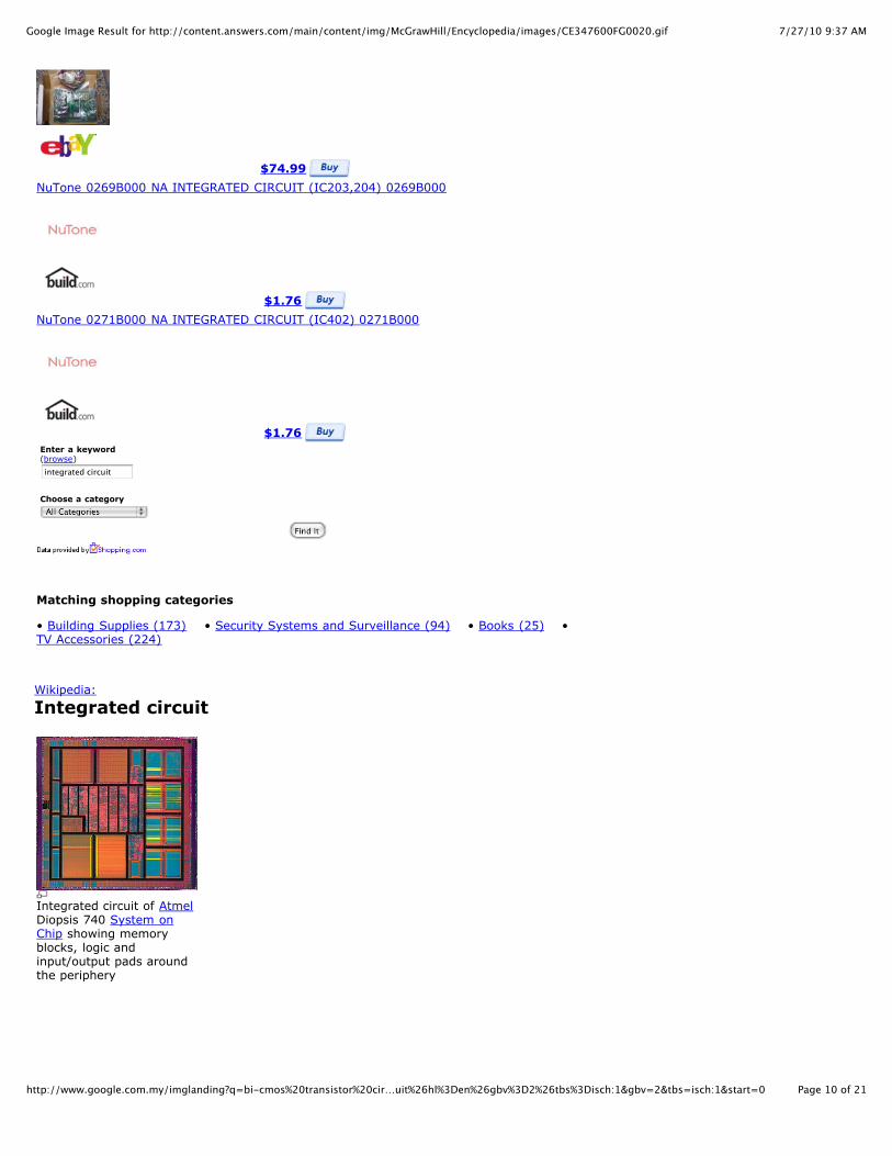
Integrated circuit
Integrated circuit of AtmelDiopsis 740 System onChip showing memoryblocks, logic andinput/output pads aroundthe periphery
7/27/10 9:37 AMGoogle Image Result for http://content.answers.com/main/content/img/McGrawHill/Encyclopedia/images/CE347600FG0020.gif
Page 11 of 21http://www.google.com.my/imglanding?q=bi-cmos%20transistor%20cir…uit%26hl%3Den%26gbv%3D2%26tbs%3Disch:1&gbv=2&tbs=isch:1&start=0
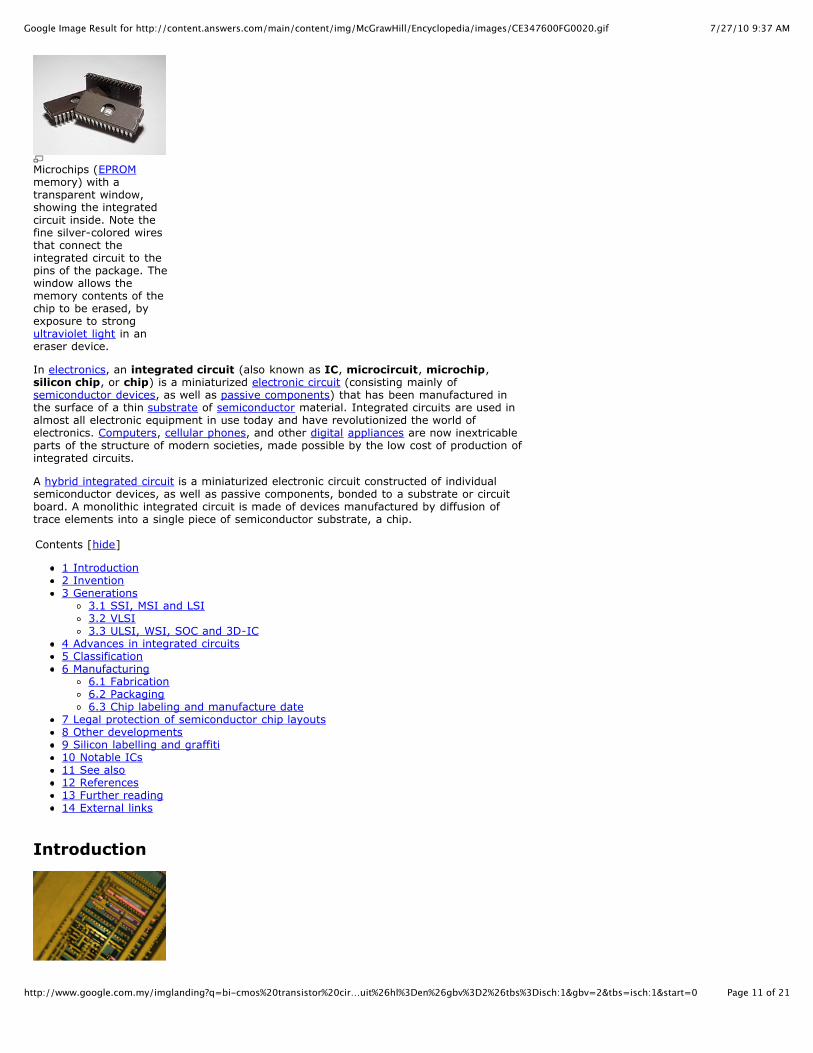
Microchips (EPROMmemory) with atransparent window,showing the integratedcircuit inside. Note thefine silver-colored wiresthat connect theintegrated circuit to thepins of the package. Thewindow allows thememory contents of thechip to be erased, byexposure to strongultraviolet light in aneraser device.
In electronics, an integrated circuit (also known as IC, microcircuit, microchip,silicon chip, or chip) is a miniaturized electronic circuit (consisting mainly ofsemiconductor devices, as well as passive components) that has been manufactured inthe surface of a thin substrate of semiconductor material. Integrated circuits are used inalmost all electronic equipment in use today and have revolutionized the world ofelectronics. Computers, cellular phones, and other digital appliances are now inextricableparts of the structure of modern societies, made possible by the low cost of production ofintegrated circuits.
A hybrid integrated circuit is a miniaturized electronic circuit constructed of individualsemiconductor devices, as well as passive components, bonded to a substrate or circuitboard. A monolithic integrated circuit is made of devices manufactured by diffusion oftrace elements into a single piece of semiconductor substrate, a chip.
Contents [hide]
1 Introduction2 Invention3 Generations
3.1 SSI, MSI and LSI3.2 VLSI3.3 ULSI, WSI, SOC and 3D-IC
4 Advances in integrated circuits5 Classification6 Manufacturing
6.1 Fabrication6.2 Packaging6.3 Chip labeling and manufacture date
7 Legal protection of semiconductor chip layouts8 Other developments9 Silicon labelling and graffiti10 Notable ICs11 See also12 References13 Further reading14 External links
Introduction
7/27/10 9:37 AMGoogle Image Result for http://content.answers.com/main/content/img/McGrawHill/Encyclopedia/images/CE347600FG0020.gif
Page 12 of 21http://www.google.com.my/imglanding?q=bi-cmos%20transistor%20cir…uit%26hl%3Den%26gbv%3D2%26tbs%3Disch:1&gbv=2&tbs=isch:1&start=0
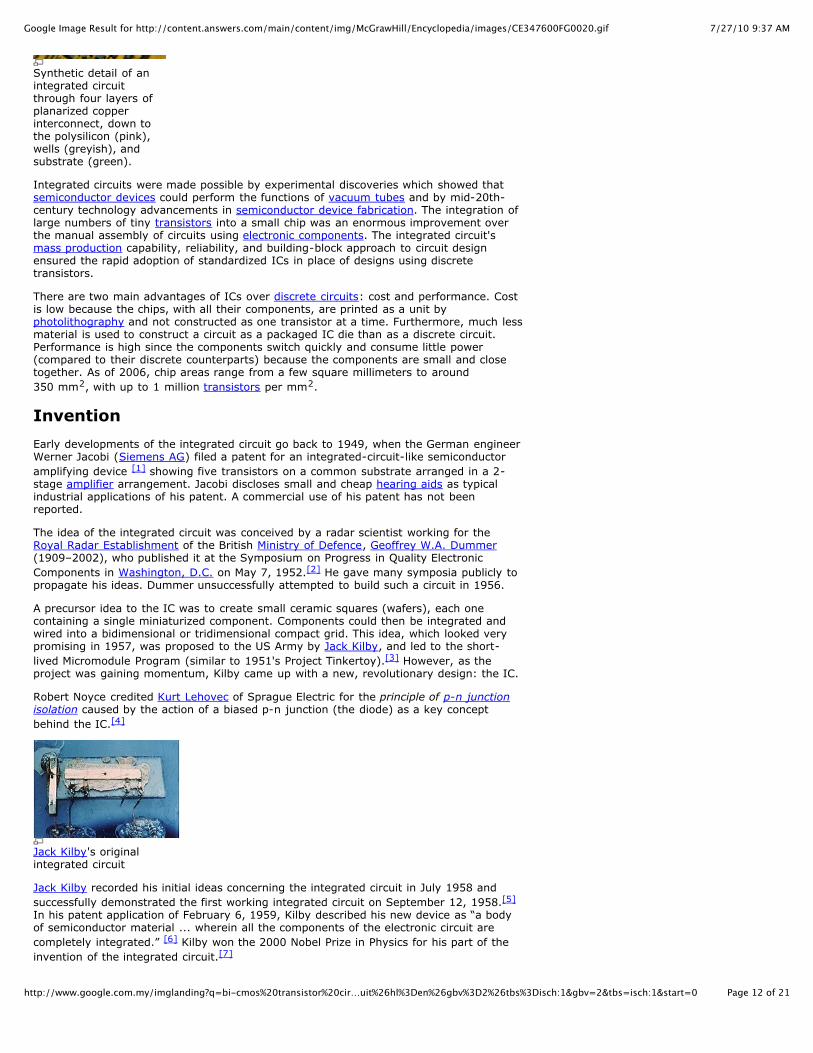
Synthetic detail of anintegrated circuitthrough four layers ofplanarized copperinterconnect, down tothe polysilicon (pink),wells (greyish), andsubstrate (green).
Integrated circuits were made possible by experimental discoveries which showed thatsemiconductor devices could perform the functions of vacuum tubes and by mid-20th-century technology advancements in semiconductor device fabrication. The integration oflarge numbers of tiny transistors into a small chip was an enormous improvement overthe manual assembly of circuits using electronic components. The integrated circuit'smass production capability, reliability, and building-block approach to circuit designensured the rapid adoption of standardized ICs in place of designs using discretetransistors.
There are two main advantages of ICs over discrete circuits: cost and performance. Costis low because the chips, with all their components, are printed as a unit byphotolithography and not constructed as one transistor at a time. Furthermore, much lessmaterial is used to construct a circuit as a packaged IC die than as a discrete circuit.Performance is high since the components switch quickly and consume little power(compared to their discrete counterparts) because the components are small and closetogether. As of 2006, chip areas range from a few square millimeters to around
350 mm2, with up to 1 million transistors per mm2.
Invention
Early developments of the integrated circuit go back to 1949, when the German engineerWerner Jacobi (Siemens AG) filed a patent for an integrated-circuit-like semiconductor
amplifying device [1] showing five transistors on a common substrate arranged in a 2-stage amplifier arrangement. Jacobi discloses small and cheap hearing aids as typicalindustrial applications of his patent. A commercial use of his patent has not beenreported.
The idea of the integrated circuit was conceived by a radar scientist working for theRoyal Radar Establishment of the British Ministry of Defence, Geoffrey W.A. Dummer(1909–2002), who published it at the Symposium on Progress in Quality Electronic
Components in Washington, D.C. on May 7, 1952.[2] He gave many symposia publicly topropagate his ideas. Dummer unsuccessfully attempted to build such a circuit in 1956.
A precursor idea to the IC was to create small ceramic squares (wafers), each onecontaining a single miniaturized component. Components could then be integrated andwired into a bidimensional or tridimensional compact grid. This idea, which looked verypromising in 1957, was proposed to the US Army by Jack Kilby, and led to the short-
lived Micromodule Program (similar to 1951's Project Tinkertoy).[3] However, as theproject was gaining momentum, Kilby came up with a new, revolutionary design: the IC.
Robert Noyce credited Kurt Lehovec of Sprague Electric for the principle of p-n junctionisolation caused by the action of a biased p-n junction (the diode) as a key concept
behind the IC.[4]
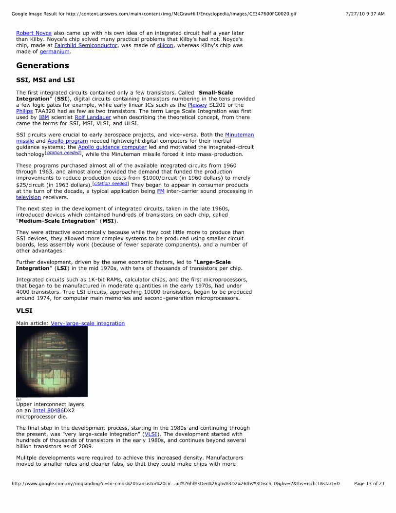
Jack Kilby's originalintegrated circuit
Jack Kilby recorded his initial ideas concerning the integrated circuit in July 1958 and
successfully demonstrated the first working integrated circuit on September 12, 1958.[5]
In his patent application of February 6, 1959, Kilby described his new device as “a bodyof semiconductor material ... wherein all the components of the electronic circuit are
completely integrated.” [6] Kilby won the 2000 Nobel Prize in Physics for his part of the
invention of the integrated circuit.[7]
7/27/10 9:37 AMGoogle Image Result for http://content.answers.com/main/content/img/McGrawHill/Encyclopedia/images/CE347600FG0020.gif
Page 13 of 21http://www.google.com.my/imglanding?q=bi-cmos%20transistor%20cir…uit%26hl%3Den%26gbv%3D2%26tbs%3Disch:1&gbv=2&tbs=isch:1&start=0
Robert Noyce also came up with his own idea of an integrated circuit half a year laterthan Kilby. Noyce's chip solved many practical problems that Kilby's had not. Noyce'schip, made at Fairchild Semiconductor, was made of silicon, whereas Kilby's chip wasmade of germanium.
Generations
SSI, MSI and LSI
The first integrated circuits contained only a few transistors. Called "Small-ScaleIntegration" (SSI), digital circuits containing transistors numbering in the tens provideda few logic gates for example, while early linear ICs such as the Plessey SL201 or thePhilips TAA320 had as few as two transistors. The term Large Scale Integration was firstused by IBM scientist Rolf Landauer when describing the theoretical concept, from therecame the terms for SSI, MSI, VLSI, and ULSI.
SSI circuits were crucial to early aerospace projects, and vice-versa. Both the Minutemanmissile and Apollo program needed lightweight digital computers for their inertialguidance systems; the Apollo guidance computer led and motivated the integrated-circuit
technology[citation needed], while the Minuteman missile forced it into mass-production.
These programs purchased almost all of the available integrated circuits from 1960through 1963, and almost alone provided the demand that funded the productionimprovements to reduce production costs from $1000/circuit (in 1960 dollars) to merely
$25/circuit (in 1963 dollars).[citation needed] They began to appear in consumer productsat the turn of the decade, a typical application being FM inter-carrier sound processing intelevision receivers.
The next step in the development of integrated circuits, taken in the late 1960s,introduced devices which contained hundreds of transistors on each chip, called"Medium-Scale Integration" (MSI).
They were attractive economically because while they cost little more to produce thanSSI devices, they allowed more complex systems to be produced using smaller circuitboards, less assembly work (because of fewer separate components), and a number ofother advantages.
Further development, driven by the same economic factors, led to "Large-ScaleIntegration" (LSI) in the mid 1970s, with tens of thousands of transistors per chip.
Integrated circuits such as 1K-bit RAMs, calculator chips, and the first microprocessors,that began to be manufactured in moderate quantities in the early 1970s, had under4000 transistors. True LSI circuits, approaching 10000 transistors, began to be producedaround 1974, for computer main memories and second-generation microprocessors.
VLSI
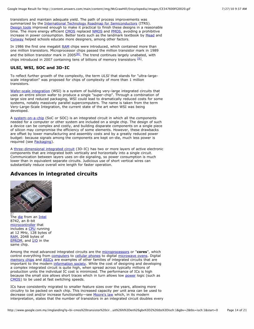
Main article: Very-large-scale integration
Upper interconnect layerson an Intel 80486DX2microprocessor die.
The final step in the development process, starting in the 1980s and continuing throughthe present, was "very large-scale integration" (VLSI). The development started withhundreds of thousands of transistors in the early 1980s, and continues beyond severalbillion transistors as of 2009.
Mulitple developments were required to achieve this increased density. Manufacturersmoved to smaller rules and cleaner fabs, so that they could make chips with more
7/27/10 9:37 AMGoogle Image Result for http://content.answers.com/main/content/img/McGrawHill/Encyclopedia/images/CE347600FG0020.gif
Page 14 of 21http://www.google.com.my/imglanding?q=bi-cmos%20transistor%20cir…uit%26hl%3Den%26gbv%3D2%26tbs%3Disch:1&gbv=2&tbs=isch:1&start=0
transistors and maintain adequate yield. The path of process improvements wassummarized by the International Technology Roadmap for Semiconductors (ITRS).Design tools improved enough to make it practical to finish these designs in a reasonabletime. The more energy efficient CMOS replaced NMOS and PMOS, avoiding a prohibitiveincrease in power consumption. Better texts such as the landmark textbook by Mead andConway helped schools educate more designers, among other factors.
In 1986 the first one megabit RAM chips were introduced, which contained more thanone million transistors. Microprocessor chips passed the million transistor mark in 1989
and the billion transistor mark in 2005[8]. The trend continues largely unabated, with
chips introduced in 2007 containing tens of billions of memory transistors [9].
ULSI, WSI, SOC and 3D-IC
To reflect further growth of the complexity, the term ULSI that stands for "ultra-large-scale integration" was proposed for chips of complexity of more than 1 milliontransistors.
Wafer-scale integration (WSI) is a system of building very-large integrated circuits thatuses an entire silicon wafer to produce a single "super-chip". Through a combination oflarge size and reduced packaging, WSI could lead to dramatically reduced costs for somesystems, notably massively parallel supercomputers. The name is taken from the termVery-Large-Scale Integration, the current state of the art when WSI was beingdeveloped.
A system-on-a-chip (SoC or SOC) is an integrated circuit in which all the componentsneeded for a computer or other system are included on a single chip. The design of sucha device can be complex and costly, and building disparate components on a single pieceof silicon may compromise the efficiency of some elements. However, these drawbacksare offset by lower manufacturing and assembly costs and by a greatly reduced powerbudget: because signals among the components are kept on-die, much less power isrequired (see Packaging).
A three-dimensional integrated circuit (3D-IC) has two or more layers of active electroniccomponents that are integrated both vertically and horizontally into a single circuit.Communication between layers uses on-die signaling, so power consumption is muchlower than in equivalent separate circuits. Judicious use of short vertical wires cansubstantially reduce overall wire length for faster operation.
Advances in integrated circuits
The die from an Intel8742, an 8-bitmicrocontroller thatincludes a CPU runningat 12 MHz, 128 bytes ofRAM, 2048 bytes ofEPROM, and I/O in thesame chip.
Among the most advanced integrated circuits are the microprocessors or "cores", whichcontrol everything from computers to cellular phones to digital microwave ovens. Digitalmemory chips and ASICs are examples of other families of integrated circuits that areimportant to the modern information society. While the cost of designing and developinga complex integrated circuit is quite high, when spread across typically millions ofproduction units the individual IC cost is minimized. The performance of ICs is highbecause the small size allows short traces which in turn allows low power logic (such asCMOS) to be used at fast switching speeds.
ICs have consistently migrated to smaller feature sizes over the years, allowing morecircuitry to be packed on each chip. This increased capacity per unit area can be used todecrease cost and/or increase functionality—see Moore's law which, in its moderninterpretation, states that the number of transistors in an integrated circuit doubles every

7/27/10 9:37 AMGoogle Image Result for http://content.answers.com/main/content/img/McGrawHill/Encyclopedia/images/CE347600FG0020.gif
Page 15 of 21http://www.google.com.my/imglanding?q=bi-cmos%20transistor%20cir…uit%26hl%3Den%26gbv%3D2%26tbs%3Disch:1&gbv=2&tbs=isch:1&start=0
two years. In general, as the feature size shrinks, almost everything improves—the costper unit and the switching power consumption go down, and the speed goes up.However, ICs with nanometer-scale devices are not without their problems, principalamong which is leakage current (see subthreshold leakage for a discussion of this),although these problems are not insurmountable and will likely be solved or at leastameliorated by the introduction of high-k dielectrics. Since these speed and powerconsumption gains are apparent to the end user, there is fierce competition among themanufacturers to use finer geometries. This process, and the expected progress over thenext few years, is well described by the International Technology Roadmap forSemiconductors (ITRS).
Classification
A CMOS 4000 IC in a DIP
Integrated circuits can be classified into analog, digital and mixed signal (both analogand digital on the same chip).
Digital integrated circuits can contain anything from one to millions of logic gates, flip-flops, multiplexers, and other circuits in a few square millimeters. The small size of thesecircuits allows high speed, low power dissipation, and reduced manufacturing costcompared with board-level integration. These digital ICs, typically microprocessors,DSPs, and micro controllers work using binary mathematics to process "one" and "zero"signals.
Analog ICs, such as sensors, power management circuits, and operational amplifiers,work by processing continuous signals. They perform functions like amplification, activefiltering, demodulation, mixing, etc. Analog ICs ease the burden on circuit designers byhaving expertly designed analog circuits available instead of designing a difficult analogcircuit from scratch.
ICs can also combine analog and digital circuits on a single chip to create functions suchas A/D converters and D/A converters. Such circuits offer smaller size and lower cost, butmust carefully account for signal interference.
Manufacturing
Fabrication
Main article: Semiconductor fabrication
Rendering of a smallstandard cell with threemetal layers (dielectrichas been removed). Thesand-colored structuresare metal interconnect,with the vertical pillarsbeing contacts, typicallyplugs of tungsten. Thereddish structures arepolysilicon gates, andthe solid at the bottomis the crystalline silicon

7/27/10 9:37 AMGoogle Image Result for http://content.answers.com/main/content/img/McGrawHill/Encyclopedia/images/CE347600FG0020.gif
Page 16 of 21http://www.google.com.my/imglanding?q=bi-cmos%20transistor%20cir…uit%26hl%3Den%26gbv%3D2%26tbs%3Disch:1&gbv=2&tbs=isch:1&start=0
bulk.
Schematic structure of aCMOS chip, as built in theearly 2000s. The graphicshows LDD-MISFET's onan SOI substrate with fivemetallization layers andsolder bump for flip-chipbonding. It also shows thesection for FEOL (front-end of line), BEOL (back-end of line) and first partsof back-end process.
The semiconductors of the periodic table of the chemical elements were identified as themost likely materials for a solid state vacuum tube by researchers like William Shockleyat Bell Laboratories starting in the 1930s. Starting with copper oxide, proceeding togermanium, then silicon, the materials were systematically studied in the 1940s and1950s. Today, silicon monocrystals are the main substrate used for integrated circuits(ICs) although some III-V compounds of the periodic table such as gallium arsenide areused for specialized applications like LEDs, lasers, solar cells and the highest-speedintegrated circuits. It took decades to perfect methods of creating crystals withoutdefects in the crystalline structure of the semiconducting material.
Semiconductor ICs are fabricated in a layer process which includes these key processsteps:
ImagingDepositionEtching
The main process steps are supplemented by doping and cleaning.
Mono-crystal silicon wafers (or for special applications, silicon on sapphire or galliumarsenide wafers) are used as the substrate. Photolithography is used to mark differentareas of the substrate to be doped or to have polysilicon, insulators or metal (typicallyaluminium) tracks deposited on them.
Integrated circuits are composed of many overlapping layers, each defined byphotolithography, and normally shown in different colors. Some layers mark wherevarious dopants are diffused into the substrate (called diffusion layers), some definewhere additional ions are implanted (implant layers), some define the conductors(polysilicon or metal layers), and some define the connections between theconducting layers (via or contact layers). All components are constructed from aspecific combination of these layers.
In a self-aligned CMOS process, a transistor is formed wherever the gate layer(polysilicon or metal) crosses a diffusion layer.
Capacitive structures, in form very much like the parallel conducting plates of atraditional electrical capacitor, are formed according to the area of the "plates", withinsulating material between the plates. Capacitors of a wide range of sizes arecommon on ICs.
Meandering stripes of varying lengths are sometimes used to form on-chip resistors,though most logic circuits do not need any resistors. The ratio of the length of the
7/27/10 9:37 AMGoogle Image Result for http://content.answers.com/main/content/img/McGrawHill/Encyclopedia/images/CE347600FG0020.gif
Page 17 of 21http://www.google.com.my/imglanding?q=bi-cmos%20transistor%20cir…uit%26hl%3Den%26gbv%3D2%26tbs%3Disch:1&gbv=2&tbs=isch:1&start=0
resistive structure to its width, combined with its sheet resistivity, determines theresistance.
More rarely, inductive structures can be built as tiny on-chip coils, or simulated bygyrators.
Since a CMOS device only draws current on the transition between logic states, CMOSdevices consume much less current than bipolar devices.
A random access memory is the most regular type of integrated circuit; the highestdensity devices are thus memories; but even a microprocessor will have memory on thechip. (See the regular array structure at the bottom of the first image.) Although thestructures are intricate – with widths which have been shrinking for decades – the layersremain much thinner than the device widths. The layers of material are fabricated muchlike a photographic process, although light waves in the visible spectrum cannot be usedto "expose" a layer of material, as they would be too large for the features. Thusphotons of higher frequencies (typically ultraviolet) are used to create the patterns foreach layer. Because each feature is so small, electron microscopes are essential tools fora process engineer who might be debugging a fabrication process.
Each device is tested before packaging using automated test equipment (ATE), in aprocess known as wafer testing, or wafer probing. The wafer is then cut into rectangularblocks, each of which is called a die. Each good die (plural dice, dies, or die) is thenconnected into a package using aluminium (or gold) bond wires which are welded and/orThermosonic Bonded to pads, usually found around the edge of the die. After packaging,the devices go through final testing on the same or similar ATE used during waferprobing. Test cost can account for over 25% of the cost of fabrication on lower costproducts, but can be negligible on low yielding, larger, and/or higher cost devices.
As of 2005, a fabrication facility (commonly known as a semiconductor lab) costs over a
billion US Dollars to construct[10], because much of the operation is automated. Themost advanced processes employ the following techniques:
The wafers are up to 300 mm in diameter (wider than a common dinner plate).Use of 65 nanometer or smaller chip manufacturing process. Intel, IBM, NEC, andAMD are using 45 nanometers for their CPU chips. IBM and AMD are in developmentof a 45 nm process using immersion lithography.Copper interconnects where copper wiring replaces aluminium for interconnects.Low-K dielectric insulators.Silicon on insulator (SOI)Strained silicon in a process used by IBM known as strained silicon directly oninsulator (SSDOI)
Packaging
Main article: Integrated circuit packaging
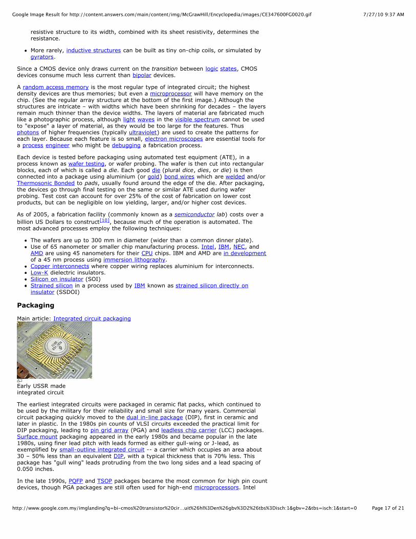
Early USSR madeintegrated circuit
The earliest integrated circuits were packaged in ceramic flat packs, which continued tobe used by the military for their reliability and small size for many years. Commercialcircuit packaging quickly moved to the dual in-line package (DIP), first in ceramic andlater in plastic. In the 1980s pin counts of VLSI circuits exceeded the practical limit forDIP packaging, leading to pin grid array (PGA) and leadless chip carrier (LCC) packages.Surface mount packaging appeared in the early 1980s and became popular in the late1980s, using finer lead pitch with leads formed as either gull-wing or J-lead, asexemplified by small-outline integrated circuit -- a carrier which occupies an area about30 – 50% less than an equivalent DIP, with a typical thickness that is 70% less. Thispackage has "gull wing" leads protruding from the two long sides and a lead spacing of0.050 inches.
In the late 1990s, PQFP and TSOP packages became the most common for high pin countdevices, though PGA packages are still often used for high-end microprocessors. Intel

7/27/10 9:37 AMGoogle Image Result for http://content.answers.com/main/content/img/McGrawHill/Encyclopedia/images/CE347600FG0020.gif
Page 18 of 21http://www.google.com.my/imglanding?q=bi-cmos%20transistor%20cir…uit%26hl%3Den%26gbv%3D2%26tbs%3Disch:1&gbv=2&tbs=isch:1&start=0
and AMD are currently transitioning from PGA packages on high-end microprocessors toland grid array (LGA) packages.
Ball grid array (BGA) packages have existed since the 1970s. Flip-chip Ball Grid Arraypackages, which allow for much higher pin count than other package types, weredeveloped in the 1990s. In an FCBGA package the die is mounted upside-down (flipped)and connects to the package balls via a package substrate that is similar to a printed-circuit board rather than by wires. FCBGA packages allow an array of input-outputsignals (called Area-I/O) to be distributed over the entire die rather than being confinedto the die periphery.
Traces out of the die, through the package, and into the printed circuit board have verydifferent electrical properties, compared to on-chip signals. They require special designtechniques and need much more electric power than signals confined to the chip itself.
When multiple dies are put in one package, it is called SiP, for System In Package. Whenmultiple dies are combined on a small substrate, often ceramic, it's called an MCM, orMulti-Chip Module. The boundary between a big MCM and a small printed circuit board issometimes fuzzy.
Chip labeling and manufacture date
Most integrated circuits large enough to include identifying information include fourcommon sections: the manufacturer's name or logo, the part number, a part productionbatch number and/or serial number, and a four-digit code that identifies when the chipwas manufactured. Extremely small surface mount technology parts often bear only anumber used in a manufacturer's lookup table to find the chip characteristics.
The manufacturing date is commonly represented as a two-digit year followed by a two-digit week code, such that a part bearing the code 8341 was manufactured in week 41 of1983, or approximately in October 1983.
Legal protection of semiconductor chip layouts
Main article: Semiconductor Chip Protection Act of 1984
Prior to 1984, it was not necessarily illegal to produce a competing chip with an identicallayout. As the legislative history for the Semiconductor Chip Protection Act of 1984, orSCPA, explained, patent and copyright protection for chip layouts, or topographies, werelargely unavailable. This led to considerable complaint by U.S. chip manufacturers—notably, Intel, which took the lead in seeking legislation, along with the SemiconductorIndustry Association (SIA)--against what they termed "chip piracy."
A 1984 addition to US law, the SCPA, made all so-called mask works (i.e., chiptopographies) protectable if registered with the U.S. Copyright Office. Similar rules applyin most other countries that manufacture ICs. (This is a simplified explanation - see SCPAfor legal details.)
Other developments
In the 1980s, programmable integrated circuits were developed. These devices containcircuits whose logical function and connectivity can be programmed by the user, ratherthan being fixed by the integrated circuit manufacturer. This allows a single chip to beprogrammed to implement different LSI-type functions such as logic gates, adders andregisters. Current devices named FPGAs (Field Programmable Gate Arrays) can nowimplement tens of thousands of LSI circuits in parallel and operate up to 1.5 GHz(Achronix holding the speed record).
The techniques perfected by the integrated circuits industry over the last three decadeshave been used to create microscopic machines, known as MEMS. These devices are usedin a variety of commercial and military applications. Example commercial applicationsinclude DLP projectors, inkjet printers, and accelerometers used to deploy automobileairbags.
In the past, radios could not be fabricated in the same low-cost processes asmicroprocessors. But since 1998, a large number of radio chips have been developedusing CMOS processes. Examples include Intel's DECT cordless phone, or Atheros's802.11 card.
Future developments seem to follow the multi-core multi-microprocessor paradigm,already used by the Intel and AMD dual-core processors. Intel recently unveiled aprototype, "not for commercial sale" chip that bears 80 microprocessors. Each core is

7/27/10 9:37 AMGoogle Image Result for http://content.answers.com/main/content/img/McGrawHill/Encyclopedia/images/CE347600FG0020.gif
Page 19 of 21http://www.google.com.my/imglanding?q=bi-cmos%20transistor%20cir…uit%26hl%3Den%26gbv%3D2%26tbs%3Disch:1&gbv=2&tbs=isch:1&start=0
capable of handling its own task independently of the others. This is in response to theheat-versus-speed limit that is about to be reached using existing transistor technology.This design provides a new challenge to chip programming. Parallel programminglanguages such as the open-source X10 programming language are designed to assist
with this task.[11]
Silicon labelling and graffiti
To allow identification during production most silicon chips will have a serial number inone corner. It is also common to add the manufactuers logo. Ever since ICs werecreated, some chip designers have used the silicon surface area for surreptitious, non-functional images or words. These are sometimes referred to as Chip Art, Silicon Art,Silicon Graffiti or Silicon Doodling.
Notable ICs
The 555 common multivibrator sub-circuit (common in electronic timing circuits)The 741 operational amplifier7400 series TTL logic building blocks4000 series, the CMOS counterpart to the 7400 series (see also: 74HC00 series)Intel 4004, the world's first microprocessor, which led to the famous 8080 CPU andthen the IBM PC's 8088, 80286, 486 etc.The MOS Technology 6502 and Zilog Z80 microprocessors, used in many homecomputers of the early 1980sThe Motorola 6800 series of computer-related chips, leading to the 68000 and88000 series (used in some Apple computers).
See also
Electronics portal
General topics
Computer engineeringElectrical engineering
Related devices and terms
Clean roomCurrent mirrorHybrid integrated circuitIon implantationMMICPhotonic integrated circuitPrinted circuit boardSilicon photonicsIntegrated circuit vacuum tube
IC device technologies
BCDMOSBiCMOSBipolar junction transistorCMOSGaAsIntegrated injection logicLogic familyMixed-signal integrated circuitMOSFETNMOSRC delaySiGe
Other
Automatic test pattern generationDatasheetArchiveHDL,MemristorMicrocontroller
7/27/10 9:37 AMGoogle Image Result for http://content.answers.com/main/content/img/McGrawHill/Encyclopedia/images/CE347600FG0020.gif
Page 20 of 21http://www.google.com.my/imglanding?q=bi-cmos%20transistor%20cir…uit%26hl%3Den%26gbv%3D2%26tbs%3Disch:1&gbv=2&tbs=isch:1&start=0
Moore's lawSemiconductor manufacturingSimulationSound chipSPICEThree-dimensional integrated circuitZIF
References
Academic
Intel 65-Nanometer TechnologyBaker, R. J. (2010). CMOS: Circuit Design, Layout, and Simulation, Third Edition.Wiley-IEEE. ISBN 978-0-470-88132-3. http://CMOSedu.com/Hodges, D.A., Jackson H.G., and Saleh, R. (2003). Analysis and Design of DigitalIntegrated Circuits. McGraw-Hill. ISBN 0-07-228365-3.Rabaey, J.M., Chandrakasan, A., and Nikolic, B. (2003). Digital IntegratedCircuits, 2nd Edition. ISBN 0-13-090996-3Mead, C. and Conway, L. (1980). Introduction to VLSI Systems. Addison-Wesley.ISBN 0-201-04358-0.
Precursors and patents
1. ^ DE patent 833366 W. Jacobi/SIEMENS AG: „Halbleiterverstärker“ priority filing onApril 14, 1949, published on May 15, 1952.
2. ^ "The Hapless Tale of Geoffrey Dummer", (n.d.), (HTML), Electronic Product News,accessed July 8, 2008.
3. ^ George Rostky, (n. d.),"Micromodules: the ultimate package", (HTML), EE Times,accessed July 8, 2008.
4. ^ Kurt Lehovec's patent on the isolation p-n junction: U.S. Patent 3,029,366granted on April 10, 1962, filed April 22, 1959. Robert Noyce credits Lehovec in hisarticle – "Microelectronics", Scientific American, September 1977, Volume 23,Number 3, pp. 63–9.
5. ^ The Chip that Jack Built, (c. 2008), (HTML), Texas Instruments, accessed May 29,2008.
6. ^ Winston, Brian. Media technology and society: a history: from the telegraph to theInternet, (1998), Routeledge, London, ISBN 041514230X ISBN 978-0415142304, p.221
7. ^ Nobel Web AB, (October 10, 2000),(The Nobel Prize in Physics 2000, Retrieved onMay 29, 2008
8. ^ Peter Clarke, EE Times: Intel enters billion-transistor processor era, 14 November2005
9. ^ Antone Gonsalves, EE Times, Samsung begins production of 16-Gb flash, 30 April2007
10. ^ For example, Intel Fab 28 cost 3.5 billion USD, while its neighboring Fab 18 cost1.5 billion USD http://www.theinquirer.net/default.aspx?article=29958
11. ^ Biever, C. "Chip revolution poses problems for programmers", New Scientist (Vol193, Number 2594)
Further reading
Invention Of Integrated Circuits: Untold Important Facts, 2009, Arjun N. Saxena,World Scientific Publishing, Singapore, ISBN 9789812814456 ISBN 9812814450
External links
Wikimedia Commons has media related to: Integrated circuit
General
Krazit, Tom "- AMD's new 65-nanometer chips sip energy but trail Intel," C-net,2006-12-21. Retrieved on January 8, 2007a large chart listing ICs by generic number and A larger one listing by mfr. number,both including access to most of the datasheets for the parts.Practical MMIC Design published by Artech House ISBN 1-59693-036-5
Author S.P. Marsh
Patents
7/27/10 9:37 AMGoogle Image Result for http://content.answers.com/main/content/img/McGrawHill/Encyclopedia/images/CE347600FG0020.gif
Page 21 of 21http://www.google.com.my/imglanding?q=bi-cmos%20transistor%20cir…uit%26hl%3Den%26gbv%3D2%26tbs%3Disch:1&gbv=2&tbs=isch:1&start=0
[hide]v • d • e
Donate to Wikimedia
US3,138,743 – Miniaturized electronic circuit – J. S. KilbyUS3,138,747 – Integrated semiconductor circuit device – R. F. StewartUS3,261,081 – Method of making miniaturized electronic circuits – J. S. KilbyUS3,434,015 – Capacitor for miniaturized electronic circuits or the like – J. S. Kilby
Audio video
A presentation of the chip manufacturing process, from Applied Materials
Silicon graffiti
The Chipworks silicon art gallery
Integrated circuit die photographs
IC Die Photography – A gallery of IC die photographs
Digital systems
Components Logic gate Digital circuit Integrated circuit (IC)
Theory Boolean logic Digital signal processing Computer architecture
Applications Digital audio Digital photography Digital video
This entry is from Wikipedia, the leading user-contributed encyclopedia. It may not havebeen reviewed by professional editors (see full disclaimer)
Related topics:
IC (abbreviation)
ASIC
known-good die (electronics)
Related answers:
What is the application of Linear integrated circuit? Read answer...
What are integrated circuits are and why? Read answer...
What are a integrated circuits? Read answer...
Help us answer these:
What is an integrated circuits?
What is circuit integration?
What is the difference between Integrated Circuits and Large scale IntegratedCircuits?
Post a question - any question - to the WikiAnswers community: