Embed Size (px)
Citation preview

User User User User’’’’s Manuals Manuals Manuals Manual
LG Programmable Logic Controller
MASTER-K
LG LG LG LG Industrial Systems
Instructions & Programming

Chapter 1 Introduction
1.1 Introductions ............................................................................. 1-1
1.2 Features ................................................................................... 1-1
Chapter 1. Introduction
1-1
1 Introductions
1.1 Introductions
The chapter 1 ‘Introduction’ will provide brief information about the features, functions, and operation of
MASTER-K series PLC.
1.2 Features
1) Features of MASTER-K series PLC are as following ;
a) various programming device for easy programming.
b) editing in RUN mode is available
c) supports various open network with international standard communication protocol.
d) realization of high processing speed with the dedicated arithmetic processor.
e) various special function modules for PLC application fields.
2) Features of MASTER-K 200S/300S/1000S are as following;
a) The fast processing speed :
Realize the lightning processing speed at 0.2 � with dedicate arithmetic processor.
b) Enhanced self-diagnostic functions :
With detailed self-diagnostic error codes, the cause of error can be identified easily.
c) Debugging operation
The MASTER-K 200S/300S/1000S provides various debugging methods as following and it
enable on-line debugging.
� execution with command by command
� execute with the break point designation
� execution according to the status of device
� execution with designated numbers of scan
d) Execution of various program types
The MASTER-K 200S/300S/1000S series provides time-driven interrupt, process-driven
interrupt, and subroutine programs as well as normal scan program.
e) Supports the sampling trace and triggering functions
The compatibility among MASTER-K series
1) The I/O (P) and data (D) registers may differ for each series. Please refer the memory map of each
series at the chapter 2.2 before convert a program for other MASTER-K series.
2) Some instructions are not supported by all series. Please refer the instruction table of appendix 9.
3) Please backup the original program before converting the program.
Remark

Chapter 2 Functions
2.1 Performance Specifications ................................................................... 2-1
2.1.1 K10S1 / K10S / K30S / K60S............................................................... 2-1
2.1.2 K200S / K300S / K1000S..................................................................... 2-2
2.2 Memory configuration map .................................................................... 2-3
2.2.1 K10S1.................................................................................................. 2-3
2.2.2 K10S / K30S / K60S............................................................................. 2-4
2.2.3 K200S / K300S / K1000S..................................................................... 2-5
2.3 Memory devices of MASTER-K series ................................................... 2-6
2.3.1 Input / output area : P .......................................................................... 2-6
2.3.2 Auxiliary relay : M................................................................................. 2-7
2.3.3 Keep relay : K ...................................................................................... 2-8
2.3.4 Link relay : L ........................................................................................ 2-8
2.3.5 Step control relay : S............................................................................ 2-8
2.3.6 Timer relay : T...................................................................................... 2-9
2.3.7 Counter relay : C................................................................................ 2-10
2.3.8 Data register : D..................................................................................2-11
2.3.9 Indirect assignment data register : #D ................................................2-11
2.3.10 Special relay : F ................................................................................. 2-12
2.3.11 Special M / L relay : M / L .................................................................. 2-12
2.3.12 Special data register : D..................................................................... 2-12
2.4 Parameter setting .................................................................................. 2-13
2.4.1 Watch dog timer setting ..................................................................... 2-13
2.4.2 Timer area setting .............................................................................. 2-13
2.4.3 The latch (non-volatile) area setting................................................... 2-13
2.4.4 Setting the mode of CPU (RUN / STOP) when an error is occurred .. 2-14
2.4.5 Station number / Baud rate setting .................................................... 2-14

2.4.6 High speed counter setting ................................................................ 2-15
2.4.7 Interrupt setting.................................................................................. 2-15
2.4.8 The reservation of I/O number allocation ........................................... 2-15
2.4.9 The output of Debug mode ................................................................ 2-16
2.5 Operation processing of CPU .............................................................. 2-17
2.5.1 The repetitive operation ..................................................................... 2-17
2.5.2 The operation mode of CPU .............................................................. 2-18
2.6 Special functions of MASTER-K series ............................................... 2-20
2.6.1 Interrupt functions .............................................................................. 2-20
2.6.2 RTC (Real Time Clock) function ........................................................ 2-24
2.6.3 Forced I/O setting .............................................................................. 2-27
2.6.4 Program edit in RUN mode................................................................ 2-28
2.6.5 Self-diagnosis .................................................................................... 2-29
2.7 Program check ...................................................................................... 2-30
2.7.1 JMP – JME......................................................................................... 2-30
2.7.2 CALL , SBRT / RET ........................................................................... 2-31
2.7.3 MCS – MCSCLR................................................................................ 2-32
2.7.4 FOR – NEXT...................................................................................... 2-33
2.7.5 END / RET ......................................................................................... 2-34
2.7.6 Dual coil ............................................................................................. 2-34
2.8 Error handling........................................................................................ 2-35
2.8.1 RUN / STOP at operation error .......................................................... 2-35
2.8.2 Error flag (F110 / F115)...................................................................... 2-35
2.8.3 LED indication.................................................................................... 2-36
2.8.4 Error code list..................................................................................... 2-37

Chapter 2. Functions
2-1
2 Functions
2.1 Performance Specifications
2.1.1 K10S1 / K10S / K30S / K60S
Items K10S1 K10S K30S K60S
Program control method Cyclic execution of stored program
I/O control method Indirect (Refresh) method
Basic 30Numbers ofInstructions
Application 226
Processing speed 3.2 ~ 7.6 ������ 1.2 ������
Program capacity 800 steps 2,048 steps
P (I/O relay)P0000 ~ P001F
(32 points)P0000 ~ P005F (96 points)
M (Auxiliary relay)M0000 ~ M015F
(256 points)M0000 ~ M031F (512 points)
K (Keep relay)K0000 ~ K007F
(128 points)K0000 ~ K015F (256 points)
L (Link relay)L0000 ~ L007F
(128 points)L0000 ~ L015F (256 points)
F (Special relay)F0000 ~ F015F
(256 points)F0000 ~ K015F (256 points)
100msT000 ~ T031(32 points)
T000 ~ T095 (96 points)T (Timer relay)
10msT032 ~ T047(16 points)
T096 ~ T127 (32 points)
C (Counter relay)C000 ~ C015
(16 points)C000 ~ C127 (128 points)
S (Step controller)S00.00 ~ S15.99(16�100 steps)
S00.00~ S31.99 (32�100 steps)
D (Data register)D0000 ~ D0063
(64 words)D0000 ~ D0255 (256 words)
The range of integer16 bit : − 32768 ~ 3276732 bit : − 2147483648 ~ 2147483647
Timer types On-delay, Off-delay, Accumulation, Monostable, Retriggerable (5 types)
Counter types Up, Down, Up-down, Ring counter (4 types)
Programming language Mnemonic, Ladder diagram
Special functions Real time clock, High speed counter, RS-485 communication
Chapter 2. Functions
2-2
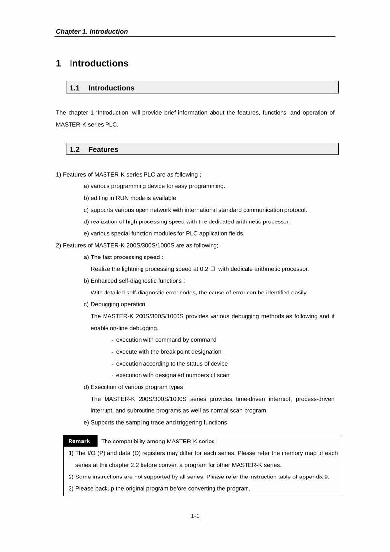
2.1.2 K200S / K300S / K1000S
Items K200S K300S K1000S
Program control methodCyclic execution of stored program, Time-driven interrupt, Event-driveninterrupt
I/O control method Indirect , Direct by program command
Basic 30Numbers ofInstructions Application 226 228
Processing speed 0.5 ������ 0.2 ������
Program capacity 7k steps 15k steps 30k steps
P (I/O relay)P0000 ~ P015F(256 points)
P0000 ~ P031F(512points)
P0000 ~ P063F(1,024 points)
M (Auxiliary relay) M0000 ~ M191F (3,072 points)
K (Keep relay) K0000 ~ K031F (512 points)
L (Link relay) L0000 ~ L063F (1,024 points)
F (Special relay) F0000 ~ F063F (1,024 points)
T (Timer relay)100msec (T000 ~ T191 : 192 points), 10msec (T192 ~ T255 : 64 points)The range of 100ms and 10ms timer can be changed with parameter setting.
C (Counter relay) C000 ~ C255 (256 points)
S (Step controller) S00.00 ~ S99.99 (100�100 steps)
D (Data register) D0000 ~ D4999 (5,000 words)D0000 ~ D9999 (10,000words)
The range of integer
1. Signed instruction16 bit : − 32768 ~ 3276732 bit : − 2147483648 ~ 2147483647
2. Unsigned instruction16 bit : 00000 ~ 6553532 bit : 00000000 ~ 4295967295
Timer types On-delay, Off-delay, Accumulation, Monostable, Retriggerable (5 types)
Counter types Up, Down, Up-down, Ring counter (4 types)
Programming language Mnemonic, Ladder diagram
Special functions Real time clock, RUN mode editing, Forced I/O control

Chapter 2. Functions
2-3
2.2 Memory configuration map
2.2.1 K10S1
Bit Data Area Word Data Area User Program Area
I/O relay
(32 points) “P”
Auxiliary relay
(256 points) “M”
Keep relay
(128 points) “K”
Special relay
(256 points) “F”
Link relay
(128 points) “L”
P00
P01
M00
M15 K00
K07F00
F15L00
L07
Data Register
(64 words)
“D”
D000
D063
Timer Setting Value
(48 words)
T000
T047T000
Timer Elapsed Value
(48 words)
Counter Setting Value
(16 words)
Counter Elapsed Value
(16 words)
T047C000
C015C000
C015
Parameter setting area
Word
User Program
Area
(800 steps)
Timer relay (100ms)
(32 points) “T”
Timer relay (10ms)
(16 points) “T”
Counter relay
(16 points) “C”
T000
T031T032
T047C000
C015
Step Controller
(16 x 100 steps)
S00.00~S15.99“S”
S00
S15
0 ~ F 0000 ~ FFFF
Retentive area
P area None T area T024 ~ T031 (10msec)
K area K000 ~ K07F T044 ~ T047 (100msec)
L area L00 ~ L07F C area C012 ~ C015
D area D048 ~ D063 S area S12.00 ~ S15.99
Chapter 2. Functions
2-4
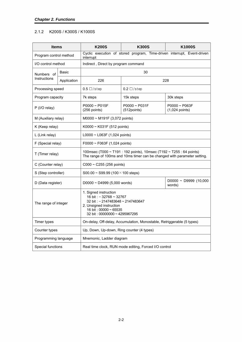
2.2.2 K10S / K30S / K60S
Bit Data Area Word Data Area User Program Area
I/O relay
(96 points) “P”
Auxiliary relay
(512 points) “M”
Keep relay
(256 points) “K”
Special relay
(256 points) “F”
Link relay
(256 points)“L”
P00
P05
M00
M31 K00
K15F00
F15L00
L15
Data Register
(256 words)
“D”
D000
D255
Timer Setting Value
(128 words)
T000
T127T000
Timer Elapsed Value
(128 words)
Counter Setting Value
(128 words)
Counter Elapsed Value
(128 words)
T127C000
C127C000
C127
Parameter setting area
Word
User Program
Area
(2,048 steps)
Timer relay (100ms)
(96 points) “T”
Timer relay (10ms)
(32 points) “T”
Counter relay
(128 points) “C”
T000
T095T096
T127C000
C127
Step Controller
(32 x 100 steps)
S00.00~S31.99“S”
S00
S31
0 ~ F 0000 ~ FFFF
Retentive area
P area None T area T072 ~ T095 (10msec)
K area K000 ~ K15F T120 ~ T127 (100msec)
L area L00 ~ L15F C area C096 ~ C127
D area D192 ~ D255 S area S24.00 ~ S31.99

Chapter 2. Functions
2-5
2.2.3 K200S / K300S / K1000S
Bit Data Area Word Data Area User Program Area
I/O relay
(See the remark) “P”
Auxiliary relay
(3,040 points) “M”
Special auxiliary relay
(32 points) “M”
Keep relay
(512 points) “K”
Special relay
(1,024 points) “F”
Link relay
(1,024 points)“L”
P00
P ✼ ✼ 1
M000
M189M190
M191 K00
K31F00
F63L00
L63
Data Register
“D”
D0000
D ✼ ✼ ✼ 2
D ✼ ✼ ✼ 3 Reserved for special usage
Timer Setting Value
(256 words)
T000
T255T000
Timer Elapsed Value
(256 words)
Counter Setting Value
(256 words)
Counter Elapsed Value
(256 words)
T255C000
C255C000
C255
Parameter setting area
Word
User Program
Area
MK1000S : 30k stepsMK300S : 15k stepsMK200S : 7k steps
Timer relay (100ms)
192points “T”
Timer relay (10ms)
64 points “T”
Counter relay
256 points “C”
T000
T191T192
T255C000
C255
Step Controller
(100 x 100 steps)
S00.00~S99.99“S”
S00
S99
P✼✼ 1 D✼✼✼✼ 2 D✼✼✼✼ 3
MK1000S P63 (1,024 pts) D9500 D9999
MK300S P31 (512 pts)
MK200S P15 (256 pts)D4500 D4999
Remark
0 ~ F 0000 ~ FFFF

Chapter 2. Functions
2-6
2.3 Memory devices of MASTER-K series
2.3.1 Input / output area : P
The P devices are used for data transaction between the PLC CPU and external devices.
The input devices hold ON/OFF data sent from external devices (e.g. pushbuttons, select
switches, limit switches, digital switches, etc.) to input module. Input data is used by the
program as contact data (NO1 and NC contacts) and as the source data for basic and
application instructions.
The output devices are used to output operation results of the program from the output module
to external devices (e.g. solenoids, magnetic switches, signal lamps, digital indicators). Only NO
contact type is available for output devices.
The redundant P devices that are not connected to external devices can be used in the same
way with the auxiliary relay M.
< Figure 1. The example of input/output configuration >
The input signals are stored in batch in the input data memory before execution of each scan.
The data in the input data memory is used for execution of the sequence program operation.
The operation results are output by each result to the output data memory. The data in the
output data memory is output in batch to the output modules after execution of the END
instruction. Please make sure that there is no conflict of input and output in the user program
because the MASTER-K series uses a P area for input and output in common.
1 NO : Normally Open contact, NC : Normally Closed contact
P0023( )
P0002
P0021
P0024( )
P0020 P0021
P0020( )
P0021( )
P0000
P0001 P0020
P0000
P0001
P0002
Input
P0020
P0021
P0023 Output
P0024

Chapter 2. Functions
2-7
< Figure 2. Flow of input / output data in the refresh mode >
- Input refresh
Input data is read (�) in batch from the input module before execution of step 0 and stored
in the input data memory.
- When an input contact command is executed :
Input data is read (�) from the input data memory and used for execution of the sequence
program.
- When an output contact command is executed :
Output data is read (�) from the output data memory and used for execution of the
sequence program.
- When an output OUT instruction is executed :
The operation result (�) is stored in the output data memory.
- Output refresh
Data (�) in the output data memory is output in batch to the output module after execution
of the END instruction.
2.3.2 Auxiliary relay : M
The M area is internal relay used in the PLC CPU, and can not be connected directly with
external devices. All M area except designated as latched area will be cleared as 0 when the
PLC is switched on or turned to RUN mode. With K200S / K300S / K1000S, a user can change
the latched area by parameter setting.
CPU Input P
Data memory
Output P
Data memory
Input
module
Output
module
� Read
� Write
CPU module
� Read
� Write
� Read
P0021
( )
P0000
P0001 P0020
P0020
( )

Chapter 2. Functions
2-8
2.3.3 Keep relay : K
The K area functions as same as M area. However, the operation results are retained if the PLC
is switched on or turned to RUN mode. The K area can be cleared by following methods;
� put the initialization routine in the sequence program.
� Run the data clear function of hand-held loader (KLD-150S)
� Run the data clear function of graphic loader (KGL-WIN)
2.3.4 Link relay : L
The L area is the internal memory for use in a data or computer link system. It can be used as
same as M area if no link module is mounted on the PLC system. With K200S / K300S /
K1000S, it is possible to change the range of latch area by parameter setting. For the detail
usage of L area, please refer the list of link relay at appendix and the computer link user’s
manual.
2.3.5 Step control relay : S
The S area can be used for two kinds of step control according to the instruction – OUT or SET.
If the OUT instruction is used, the S area functions as last-in priority. Otherwise, it functions as
sequential control. (See the chapter 4 for detailed usage.)
When the CPU is switched on or turned to RUN mode, the S area will be initialized as first step
(Sxx.00) except the latch area designated by parameter setting.
OUT S00.02
OUT S00.29
OUT S00.61
In the same group, the last-in condition has the
priority to run.
SET S00.01
SET S00.02
SET S00.03
Sequential control means that a certain process
can be executed only after the previous process
is completed.
SET S00.04
SET S00.00The clear condition (Sxx.00 ) can be operated at
any time while the sequential process is
running.

Chapter 2. Functions
2-9
2.3.6 Timer relay : T
MASTER-K series have 100msec and 10msec timer. The timing method is various according to
the timer instructions (TON, TOFF, TMR, TMON, TRTG). The maximum timer setting value is
hFFFF by hexadecimal or 65535 by decimal. The following figure shows the types and timing
methods of each timer instruction.
< Figure 3. Types and timing methods of timer instructions >
Timerinstruction
DescriptionTimingmethod
Time chart
TON ON Delay Increment
TOFF OFF Delay Decrement
TMRAccumulation
ON Delay Increment
TMON Monostable Decrement
TRTG Retriggerable Decrement
Timerinstruction
No. of timer relayInput contact Setting value
ON Delay timerInputcondition
t
t =setting value
OFF Delay timer
t
Accumulationtimer
t1 t2
t = t1 + t2
Monostable timer
t
Retriggerable timert
Timeroutput
Inputcondition
Timeroutput
Timeroutput
Timeroutput
Timeroutput
Inputcondition
Inputcondition
Inputcondition
t =setting value
t =setting value
t =setting value
t =setting value
Chapter 2. Functions
2-10
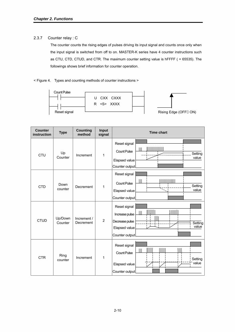
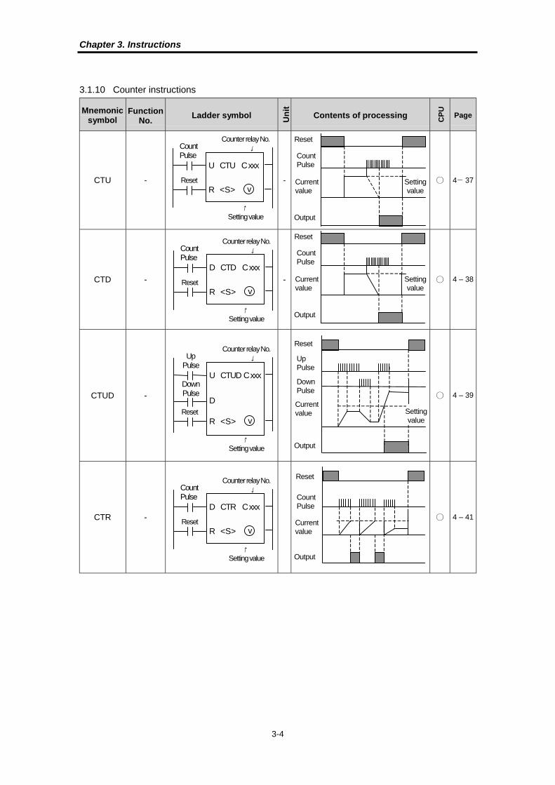
2.3.7 Counter relay : C
The counter counts the rising edges of pulses driving its input signal and counts once only when
the input signal is switched from off to on. MASTER-K series have 4 counter instructions such
as CTU, CTD, CTUD, and CTR. The maximum counter setting value is hFFFF ( = 65535). The
followings shows brief information for counter operation.
< Figure 4. Types and counting methods of counter instructions >
Counterinstruction
TypeCountingmethod
Inputsignal
Time chart
CTUUp
CounterIncrement 1
CTDDown
counterDecrement 1
CTUDUp/DownCounter
Increment /Decrement
2
CTRRing
counterIncrement 1
Rising Edge (OFF→ON)
U CXX CXXX
R <S> XXXX
Settingvalue
Reset signal
Count Pulse
Elapsed value
Counter output
Increase pulse
Decrease pulse
Settingvalue
Settingvalue
Reset signal
Count Pulse
Elapsed value
Counter output
Elapsed value
Counter output
Reset signal
Reset signal
Count Pulse
Elapsed value
Counter output
Settingvalue
Reset signal
Count Pulse

Chapter 2. Functions
2-11
2.3.8 Data register : D
The D area is used to store numeric data. Each data register consists of 16 bits (1 word) which
is the unit of data read and write.
The data resister number designated by the double-word instruction holds the lower 16 bits and
the designated data register number + 1 holds the higher 16 bits.
Example)
D51 D50
h1234 h5678
The D area except latched area assigned by parameter setting will be cleared as 0 when the
CPU is switched on or turned to RUN mode.
2.3.9 Indirect assignment data register : #D
#D is used for indirect addressing of the D area. The contained value of data register assigned
with ‘#’ symbol points the real address of data register at which the result of operation is stored.
If #D is used with a double-word instruction, the lower 16 bits will stored at the data resister
number designated by the contained value of #D, and higher 16 bits will stored at the data
resister number + 1.
Example)
DMOV h12345678 D050
High 16 bits Lower 16 bits
MOV D000 #D1023
h7893
h03E8(1000)
(Hex value)(No. of data register)
D0000
D1000
D1023
The actual data movement
Indirect addressing (#D0123)
If the value of data register assigned at # D exceeds the physical address range of D area, the operation error
flag(F110) will be set and the relevant instruction will be ignored.
Remark
Chapter 2. Functions
2-12
2.3.10 Special relay : F
The F area is read-only relay and user can not change the value of F area. See the F relay table
at the appendix for details.
2.3.11 Special M / L relay : M / L
Some M or L relays are reserved for special usage. See the list of special relays at the appendix
and be careful when use those M or L area in the program.
2.3.12 Special data register : D
Some data registers are reserved for special usage. These registers are various according to
the type of CPU. See the list of special registers at the appendix and be careful when use those
data register in the program.
Chapter 2. Functions
2-13
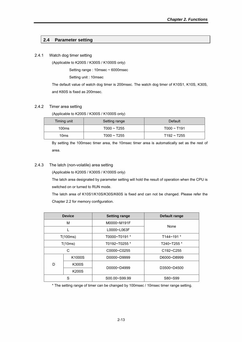
2.4 Parameter setting
2.4.1 Watch dog timer setting
(Applicable to K200S / K300S / K1000S only)
Setting range : 10msec ~ 6000msec
Setting unit : 10msec
The default value of watch dog timer is 200msec. The watch dog timer of K10S1, K10S, K30S,
and K60S is fixed as 200msec.
2.4.2 Timer area setting
(Applicable to K200S / K300S / K1000S only)
Timing unit Setting range Default
100ms T000 ~ T255 T000 ~ T191
10ms T000 ~ T255 T192 ~ T255
By setting the 100msec timer area, the 10msec timer area is automatically set as the rest of
area.
2.4.3 The latch (non-volatile) area setting
(Applicable to K200S / K300S / K1000S only)
The latch area designated by parameter setting will hold the result of operation when the CPU is
switched on or turned to RUN mode.
The latch area of K10S1/K10S/K30S/K60S is fixed and can not be changed. Please refer the
Chapter 2.2 for memory configuration.
Device Setting range Default range
M M0000~M191F
L L0000~L063FNone
T(100ms) T0000~T0191 * T144~191 *
T(10ms) T0192~T0255 * T240~T255 *
C C0000~C0255 C192~C255
K1000S D0000~D9999 D6000~D8999
K300SD
K200SD0000~D4999 D3500~D4500
S S00.00~S99.99 S80~S99
* The setting range of timer can be changed by 100msec / 10msec timer range setting.

Chapter 2. Functions
2-14
2.4.4 Setting the mode of CPU (RUN / STOP) when an error is occurred
(Applicable to K200S / K300S / K1000S only)
When a non-critical error such as fuse blown or operation error, the CPU will keep running or
stop operation according to the parameter setting. See the following table for details.
(K10S1/K10S/K30S/K60S is set as the default setting of K200S/300S/1000S.)
* = Default setting
Error type Description ModeRUN
LEDError flag
Fuse blownThe fuse of output or hybrid module is
blown
RUN * /
STOP
ON * /
OFFF035
Operation
Error
BCD error
The result of BCD conversion is
exceeds the specified range (9999 or
99999999)
Over range error
One or more operands exceed the
specified device range.
RUN * /
STOP
ON * /
OFF
F110
F115
The F110 bit is updated after each instruction is completed. Therefore, even an operation error
was occurred, the F110 will be cleared if the next instruction is completed normally. In other
hand, the F115 will be set when an operation error occurs and keep the on status until user
cleared the F115 with CLE instruction.
2.4.5 Station number / Baud rate setting
(Applicable for K10S1 / K10S / K30S / K60S / K200S)
PLC type Protocol Station number Baud rate Descriptions
K10S1
K10S
K30S
K60S
RS-4850 ~ 31
(h00 ~ h1F)
300, 600, 1200, 2400, 4800,
9600, 19200 bps
K200S-A2 RS-232 N/A 9600, 19200, 38400 bps
K200S-B/C3 RS-422 0 ~ 31
2 K3P-07AS3 K3P-07BS / K3P-07CS

Chapter 2. Functions
2-15
2.4.6 High speed counter setting
(Applicable for K10S1, K10S, K30S, K60S)
The block type models of MASTER-K series include the high speed counter function in the main
module. When the ‘HSCNT’ instruction is used, the high speed counter parameters should be
set with KGL-WIN or KLD-150S. Refer the 5.22.1 ‘HSCNT’ instruction part.
2.4.7 Interrupt setting
(Applicable for K200S / K300S / K1000S)
1) The priority of interrupts setting
Each of interrupts has a priority level. If two or more interrupts occur at the same time, the CPU
will process the interrupt that has higher priority. Priority levels are described by numbers, and
smaller number means higher priority.
2) TDI (Time driven interrupt)
TDI is the interrupt that occurs periodically. The period of interrupt can be set with parameters
by 10-msec unit. The longest period is 60 seconds.
3) PDI (Process driven interrupt)
PDI is the interrupt that occurs when an input of interrupt module was turned on.
Refer the chapter 2.6.1 for more details.
2.4.8 The reservation of I/O number allocation
(Applicable for K200S / K300S / K1000S)
The I/O number is allocated automatically by CPU module according to the actual status of
module. However, user can reserve I/O number allocation with parameter setting, then it makes
a user keep a sequence program in case of module fault or replacement.
1) User can assign the type of module (input, output, or special module) and I/O occupation
number to each module.
2) If the reserved I/O number is larger than the I/O number of actual module, the redundant
reserved I/O points are used as internal relay. Otherwise, the redundant actual I/O points are
disabled.
3) Non-reserved slots occupy I/O points as the I/O points of actual module, and special
modules occupy 16 I/O points.
Chapter 2. Functions
2-16
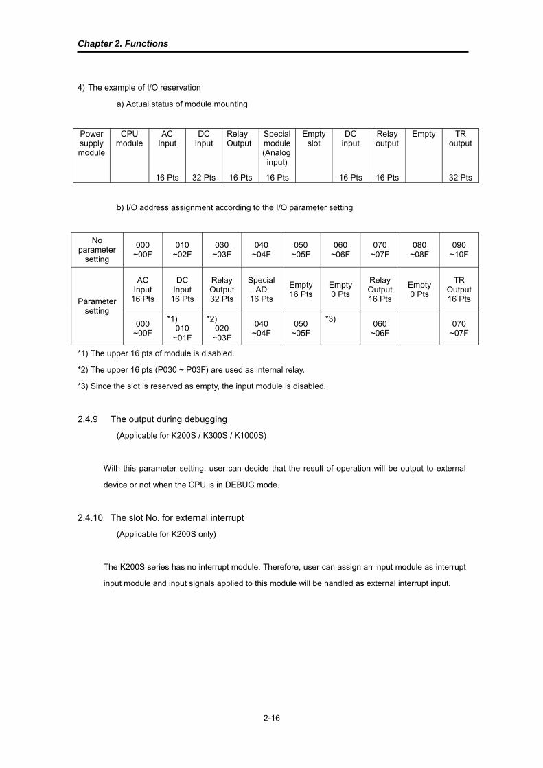
4) The example of I/O reservation
a) Actual status of module mounting
Powersupplymodule
CPUmodule
ACInput
DCInput
RelayOutput
Specialmodule(Analoginput)
Emptyslot
DCinput
Relayoutput
Empty TRoutput
16 Pts 32 Pts 16 Pts 16 Pts 16 Pts 16 Pts 32 Pts
b) I/O address assignment according to the I/O parameter setting
Noparameter
setting
000~00F
010~02F
030~03F
040~04F
050~05F
060~06F
070~07F
080~08F
090~10F
ACInput
16 Pts
DCInput
16 Pts
RelayOutput32 Pts
SpecialAD
16 Pts
Empty16 Pts
Empty0 Pts
RelayOutput16 Pts
Empty0 Pts
TROutput16 PtsParameter
setting
000~00F
*1)010
~01F
*2)020
~03F
040~04F
050~05F
*3)060
~06F070
~07F
*1) The upper 16 pts of module is disabled.
*2) The upper 16 pts (P030 ~ P03F) are used as internal relay.
*3) Since the slot is reserved as empty, the input module is disabled.
2.4.9 The output during debugging
(Applicable for K200S / K300S / K1000S)
With this parameter setting, user can decide that the result of operation will be output to external
device or not when the CPU is in DEBUG mode.
2.4.10 The slot No. for external interrupt
(Applicable for K200S only)
The K200S series has no interrupt module. Therefore, user can assign an input module as interrupt
input module and input signals applied to this module will be handled as external interrupt input.

Chapter 2. Functions
2-17
2.5 Operation processing of CPU
2.5.1 The repetitive operation
The repetitive operation method repeats execution of a series of operations The CPU repeats
the operation processing as followings.
Fig. 2-3 Operation processing of the CPU
The CPU refreshes input data, then executes the sequence program stored in the internal
memory, beginning with step 0 to the END instruction. After executing the END instruction, the
CPU performs self-diagnosis and refreshes output data, and then returns to input refresh.
Input refresh
Step : 0000
Step : 0001
:
:
END
Self-diagnosis
Output refresh
1 Scan
Operation
Scan : The series of steps from step 0 to the next step 0 is called a scan. Therefore, a scan time of the CPU is
calculated as a total of the processing time of the sequence program (step 0 to END) and the internal
processing time (self-diagnosis and I/O refresh) of the CPU.
Remark

Chapter 2. Functions
2-18
2.5.2 The operation mode of CPU
MASTER-K series has 4 operation modes as shown below. The arrow indicates that mode
change is available.
<Figure 2-4 Operation modes of MASTER-K series>
1) The flow of RUN mode
*1) END processing : Self-diagnosis, Timer / Counter update
RUN
mode
Pause
mode
Program
mode
Debug
mode
Start RUN mode
Clear the non-latched
memory area
Check user program
Execution of
sequence program
END processing *1)
I/O refresh
Check mode change

Chapter 2. Functions
2-19
2) The flow of Program (PGM) mode
- Program read / write / monitor can be performed in program mode. External wiring check is also
possible with the forced I/O on/off function.
3) The flow of Pause mode
- Stops the operation of CPU, but keep the status of output and internal memory.
4) The flow of Debug mode
Start PGM mode
Turn the output off
Self-diagnosis
I/O refresh
Check mode change
Start Pause mode
Self-diagnosis
Check mode change
Start Debug mode
Clear non-latched memory area
Stop operation
Self-diagnosis
I/O refresh
Check mode change
Execute the operation at
The designated step

Chapter 2. Functions
2-20
2.6 Special functions of MASTER-K series
2.6.1 Interrupt functions
(Applicable for K200S / K300S / K1000S )
When an interrupt occurs, the CPU module will stop the current operation and execute the
corresponding interrupt routine. After finish the interrupt routine, the CPU resume the sequence
program from the stopped step.
MASTER-K series provides 2 types of interrupt. The TDI (Time driven interrupt) occurs with the
constant period, and PDI (Process driven interrupt) occurs with the status of external input.
Before to use interrupt function in sequence program, the parameter setting should be done
properly. (See 2.4.6 for parameter setting) Then the corresponding interrupt routine should be
written after END instruction. (Refer chapter 4 for details) If interrupt routines are not matched with
parameter settings, an error occurs and the operation of CPU will be stopped.
To execute an interrupt routine, use the EI instruction to enable the corresponding interrupt. The
interrupt routine is not executed if an interrupt factor occurs before execution of an EI instruction.
Once an interrupt is enabled with EI instruction, it keeps the enabled status until DI instruction is
executed to disable the interrupt. When a CPU is turned to RUN mode, all interrupts are disabled
by default.
When multiple interrupt factors occur simultaneously, interrupt routines are executed according to
the priority given to the each interrupts. If an interrupt factor that has higher priority occurs while
other interrupt that has lower priority are executing, the interrupt routine of lower priority will be
stopped and the interrupt of higher priority will be executed first. The following figure shows how a
CPU handle multiple interrupts.
<Figure 2. 5 The execution order of multiple interrupts>
Program starts
Interrupt 2 occurs
Stop main program and execute interrupt
routine 2
Interrupt 1 occurs (higher priority)
Stop routine 2 and run routine 1
Finish routine 1 and return to routine2
Main Program
Interrupt routine 1
Interrupt routine 2
1
3
5
6
7
2
4
Finish routine 2 and return to main program
1
2
3
4
5
6
7
Chapter 2. Functions
2-21
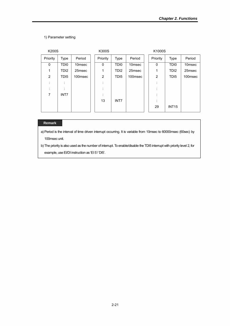
1) Parameter setting
K200S K300S K1000S
Priority Type Period Priority Type Period Priority Type Period
0
1
2
:
:
7
TDI0
TDI2
TDI5
:
:
INT7
10msec
25msec
100msec
0
1
2
:
:
:
13
TDI0
TDI2
TDI5
INT7
10msec
25msec
100msec
0
1
2
:
:
:
:
29
TDI0
TDI2
TDI5
INT15
10msec
25msec
100msec
a) Period is the interval of time driven interrupt occurring. It is variable from 10msec to 60000msec (60sec) by
100msec unit.
b) The priority is also used as the number of interrupt. To enable/disable the TDI5 interrupt with priority level 2, for
example, use EI/DI instruction as ‘EI 5’/ ‘DI5’.
Remark

Chapter 2. Functions
2-22
2) TDI (Time driven interrupt)
TDI occurs periodically with the constant interval assigned in parameter setting. The interrupt
routine of TDI starts with the TDINT instruction and ends with the IRET instruction.
When multiple interrupt factors occur simultaneously, interrupt routines are executed according
to the priority given to the each interrupt. If an interrupt factor has higher priority occurs while
other interrupt has lower priority are executing, the interrupt routine of lower priority will be
stopped and the interrupt of higher priority will be executed first. Otherwise, two interrupts are
executed consequently.
The maximum numbers of TDI for K200S / 300S / 1000S are shown as following table. See the
2.4.5 for details of parameter setting.
PLC type Available TDI
K200S TDINT 0 ~ 7
K300S TDINT 0 ~ 13
K1000S TDINT 0 ~ 29
The following figure shows an example of TDI execution.
<Figure 2.6 The example of execution of TDI>
Used TDI
TDI 0 : occurs every 200msec
TDI 1 : occurs every 100msec
TDI 2 : occurs every 400msec
A B C A B A B CB B
100msec 100msec 100msec 100msec
200msec
400msec
200msec
Interrupt routines
A : The routine corresponding to TDI 0
B : The routine corresponding to TDI 1
C : The routine corresponding to TDI 2

Chapter 2. Functions
2-23
3) PDI (Process driven interrupt)
PDI occurs when the input status of interrupt module is changed from OFF to ON or from ON to
OFF. (Select by DIP switch setting) Since K200S does not have interrupt module, PDI will occur
when the input assigned as interrupt input by parameter setting is changed from OFF to ON.
The execution order of multiple interrupts is similar as TDI. The following figure shows an
example of execution order of multiple PDI.
<Figure 2-7 The execution order of multiple PDI>
Main Program
Interrupt routine 0
Interrupt routine 1
1
3
5
7
8
2
4Interrupt routine 2
6
PDI 0
PDI 1
PDI 2
2 4 6
9
Program starts
Interrupt 2 occurs
Stop main program and run PDI routine 2
Interrupt 0 occurs (higher priority)
Stop routine 2 and execute routine 0
Interrupt 1 occurs (lower priority)
Finish routine 0 and execute routine 1
Finish routine 1 and resume routine 2
Finish routine 2 and back to main program
1
2
3
4
5
6
7
8
9

Chapter 2. Functions
2-24
2.6.2 RTC (Real Time Clock) function
Since the RTC function is optional function, not all MASTER-K series support this function.
Please refer the Catalog and CPU manual for applicable models.
Clock operation by the RTC function is continued with a battery or super capacitor when the
CPU is powered off.
1) Clock data
Clock data is the data comprised of year, month, day, hour, minute, second, and date.
Data name Description
Year The lower 2 digits of the Christian Era
Month 1 to 12
Day 1 to 31 (A leap year is distinguished automatically)
Hour 0 to 23 (24 hours)
Minute 0 to 59
Second 0 to 59
0 Sunday
1 Monday
2 Tuesday
3 Wednesday
4 Thursday
5 Friday
Date
6 Saturday
2) Precision
Max. 1.728 second per day (general temperature)
3) K10S / K30S / K60S
a) Read RTC data
RTC data is stored as following table.
DescriptionMemory Area(Word) Higher byte Lower byte
Example data(BCD format)
L012 Year - h98xx
L013 Day Month h2212
L014 Hour Date h1902
L015 Second Minute h4637
Example : 1998. 12. 22. 19:37:46, Tuesday
Chapter 2. Functions
2-25
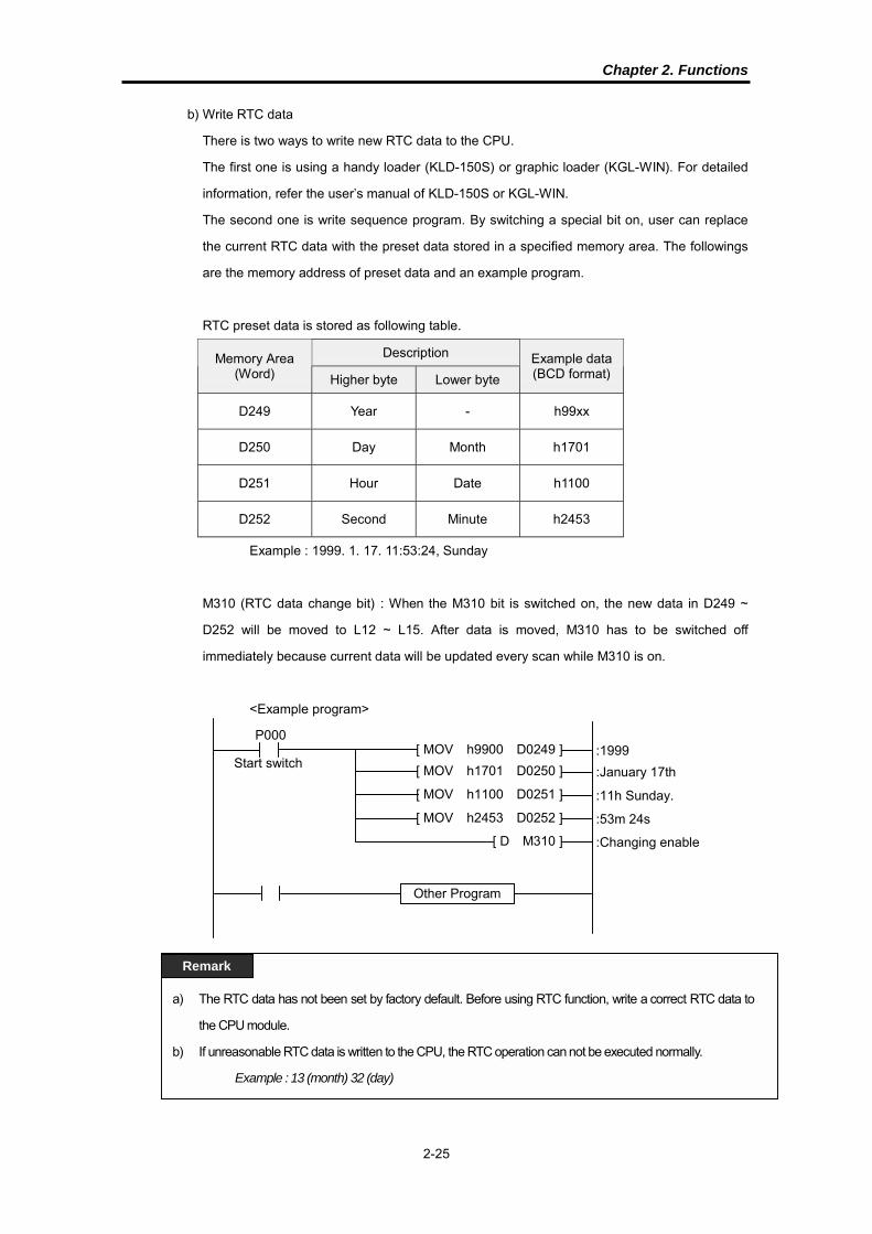
b) Write RTC data
There is two ways to write new RTC data to the CPU.
The first one is using a handy loader (KLD-150S) or graphic loader (KGL-WIN). For detailed
information, refer the user’s manual of KLD-150S or KGL-WIN.
The second one is write sequence program. By switching a special bit on, user can replace
the current RTC data with the preset data stored in a specified memory area. The followings
are the memory address of preset data and an example program.
RTC preset data is stored as following table.
DescriptionMemory Area(Word) Higher byte Lower byte
Example data(BCD format)
D249 Year - h99xx
D250 Day Month h1701
D251 Hour Date h1100
D252 Second Minute h2453
Example : 1999. 1. 17. 11:53:24, Sunday
M310 (RTC data change bit) : When the M310 bit is switched on, the new data in D249 ~
D252 will be moved to L12 ~ L15. After data is moved, M310 has to be switched off
immediately because current data will be updated every scan while M310 is on.
<Example program>
[ MOV h9900 D0249 ]
[ MOV h1701 D0250 ]
[ MOV h1100 D0251 ]
[ MOV h2453 D0252 ]
[ D M310 ]
Start switch
P000
Other Program
:1999
:January 17th
:11h Sunday.
:53m 24s
:Changing enable
a) The RTC data has not been set by factory default. Before using RTC function, write a correct RTC data to
the CPU module.
b) If unreasonable RTC data is written to the CPU, the RTC operation can not be executed normally.
Example : 13 (month) 32 (day)
Remark

Chapter 2. Functions
2-26
4) K200S / K300S / K1000S
To read / write RTC data of K200S / K300S / K1000S is similar as K10S / K30S / K60S. The
only difference is memory address of current / preset RTC data. See the following table.
The current RTC data
DescriptionMemory Area(Word) Higher byte Lower byte
Data(BCD format)
F053 Year Month h9812
F054 Day Hour h2219
F055 Minute Second h3746
F056 - Date hxx02
Example : 1998. 12. 22. 19:37:46, Tuesday
The preset RTC data
Memory Area (Word) Description
K200S / K300S K1000S Higher byte Lower byte
Data(BCD format)
D4990 D9990 Year Month h9901
D4991 D9991 Day Hour h1711
D4992 D9992 Minute Second h5324
D4993 D9993 - Date hxx00
Example : 1999. 1. 17. 11:53:24, Sunday
M1904 : RTC data change bit
When the M1904 bit is switched on, the new data in D4990 ~ D4993 (D9990 ~ D9993) will be
moved to F53 ~ F56. After data is moved, M1904 has to be switched off immediately
because current data will be updated every scan while M1904 is on.
<Example program for K200S / K300S>
[ MOV h9901 D4990 ]
[ MOV h1711 D4991 ]
[ MOV h5324 D4992 ]
[ MOV h0000 D4993 ]
[ D M1904 ]
Start switch
P000
Other Program
:1999 January
:17th 11 o’clock
:53min 24sec
:Sunday
:Changing enable

Chapter 2. Functions
2-27
2.6.3 Forced I/O setting
(Applicable for K200S / K300S / K1000S)
It is possible to output a designated data regardless of the result of operation. This function is
useful to check operation of the output modules and wiring between the output modules and
external devices.
K200S K300S K1000S
Forced I/O request bit M1910
The forced I/O address D4700 ~ D9700 ~
The forced I/O data D4800 ~ D9800 ~
Example 1) Output h8721 to the P10 word by force (K200S / K300S)
a) Write the forced I/O data (h8721) to the corresponding data word. P10 is matched to the
D4810 word.
<D4810 word>
F E D C B A 9 8 7 6 5 4 3 2 1 0
1 0 0 0 0 1 1 1 0 0 1 0 0 0 0 1
b) Write the forced I/O address (All bit = hFFFF) to the corresponding address word. Write
hFFFF to the D4710.
<D4710 word> ( 0 = disable forced I/O, 1 = enable forced I/O )
F E D C B A 9 8 7 6 5 4 3 2 1 0
1 1 1 1 1 1 1 1 1 1 1 1 1 1 1 1
c) Switch on the forced I/O request bit (M1910).
d) Output of P10 word
(P : The previous result of operation)
F E D C B A 9 8 7 6 5 4 3 2 1 0
P P P P P P P P P P P P P P P P
F E D C B A 9 8 7 6 5 4 3 2 1 0
1 0 0 0 0 1 1 1 0 0 1 0 0 0 0 1

Chapter 2. Functions
2-28
Example 2) Switch On/Off the last bit of P07 word (K1000S)
a) Write the forced I/O data (h0001) to the corresponding data word. P10 is matched to the
D9807 word.
<D9807 word>
F E D C B A 9 8 7 6 5 4 3 2 1 0
0 0 0 0 0 0 0 0 0 0 0 0 0 0 0 1
b) Write the forced I/O address (last bit = h0001) to the corresponding address word. Write
h0001 to the D9707.
<D9707 word> ( 0 = disable forced I/O, 1 = enable forced I/O )
F E D C B A 9 8 7 6 5 4 3 2 1 0
0 0 0 0 0 0 0 0 0 0 0 0 0 0 0 1
c) Switch on the forced I/O request bit (M1910).
d) Output of P07 word
(P : The previous result of operation)
F E D C B A 9 8 7 6 5 4 3 2 1 0
P P P P P P P P P P P P P P P P
F E D C B A 9 8 7 6 5 4 3 2 1 0
P P P P P P P P P P P P P P P 1
2.6.4 Program edit in RUN mode
(Applicable for K200S / K300S / K1000S)
User can insert, delete, or change instructions of program while the CPU is running. This
function is useful to debugging or test-operation. Please refer the user’s manual of KLD-150S or
KGL-WIN for detail information.
The program edit in RUN mode can not be performed for the following instructions – JMP, JME, CALL, SBRT,
FOR, and NEXT instructions. Moreover, the program that has very long scan time (longer than 2 seconds) can
not be edit while the CPU is in the RUN mode.
Remark

Chapter 2. Functions
2-29
2.6.5 Self-diagnosis
1) WDT (Watch dog timer) function
The watch dog timer is an internal timer of a PLC to detect the error of hardware and a
sequence program. The default value is set as 200msec, and it is changeable with parameter
setting. (K200S / K300S / K1000S only) Refer 2.4.1 for details on the parameter setting.
The CPU resets the watch dog timer before step 0 is executed (after the END processing is
finished). When the END instruction has not been executed within the set value due to an error
occurred in the PLC or the long scan time of a sequence program, the watch dog timer will
times out. When a watch dog timer error is occurred, all outputs of the PLC are turned OFF, and
the ERR LED of the CPU will flashes. (RUN LED will be turned OFF) Therefore, when use FOR
~ NEXT or CALL instruction, insert WDT instruction to reset the watch dog timer.
2) I/O module check function
If one or more I/O modules are mounted/dismounted while the PLC is powered, the
corresponding bit (F0040 ~ F0050 : 32 bits) will be switched on. If a module is mounted
improperly, the relevant bit will be switched on also.
3) Battery check function
(Applicable for K200S / K300S / K1000S)
When the voltage of the battery for back-up the memory IC of CPU are lower than the minimum
back-up voltage, the BAT LED of CPU module will be turned on.
1 1 1
1 1 1
P
W
R
Slot No : 0
C
P
U
1 2 3 4 5 6 7
Error occurred at slot 0
Error occurred at slot 1
Error occurred at slot 15
Error occurred at slot 31
F004
(word)
F005
(word)
MSB
MSB
LSB
LSB

Chapter 2. Functions
2-30
2.7 Program check
2.7.1 JMP – JME
1) If the input condition of JMP n instruction is turned on, the CPU skips all instructions until JME n
instruction. The skipped instructions are processed as NOP instruction. Max. 128 JMP-JME can be
used. (JMP 0 ~ JMP 127, JME 0 ~ JME 127)
JMP 000
LOAD P0000
OUT P001
JME 000
2) The JMP n instruction should be matched only one JME n instruction. The duplication of JME is not
permitted. However, the duplication of JMP n instructions is possible.
3) The JMP n instruction without corresponding JME n instruction (stand-alone JMP n) will cause
program error. If only JME or JMP is inside of a loop (subroutine, FOR~NEXT block, or interrupt
routine), an operation error will occur when the JMP instruction is enabled.
JMP 005 : Error (Stand-alone)
MOV
END
JMP 005 : Error when it is enabled
FOR 50
JME 005
NEXT
Process
as ‘NOP’
JMP 001
JME 001
JME 001
Error
JMP 001
JMP 001
JME 001
No Error
JME 001JME 001

Chapter 2. Functions
2-31
2.7.2 CALL , SBRT / RET
1) CALL n, CALLP n :
The CALL(P) instruction executes the subroutine program specified by the pointer ‘n’. Multiple
levels of nesting of the CALL(P) instruction are allowed.
2) SBRT / RET
SBRT instruction shows the start of subroutine program, and RET shows the end. Those two
instructions should be in pairs.
LOAD P000
SBRT 40 : Error (SBRT before END)
END
RET : Error (Stand Alone)
LOAD P042
CALL 30 : Error (No SBRT)
END
LOAD P010
CALL 30
END
SBRT 30 : Error (No RET)

Chapter 2. Functions
2-32
2.7.3 MCS – MCSCLR
The MCS n instruction starts a master control sequence. Each MCS instructions are followed by
a number (n) that shows the priority of the master control. The range of n is 0 ~ 7.
MCS 0 : High
↕
MCS 7 : LOW
The MCSCLR n instruction ends a master control sequence. If a MCSCLR instruction is
executed, all master controls that have lower priority are cleared automatically.
MCS 0
MCS 1
MCSCLR 0 : (MCS 1 is cleared automatically)
MCSCLR 1 : Error (Improper order of MCSCLR)
When use master control, it should start from the highest priority level and end from the lowest
priority level. The MCS n and MCSCLR n instructions should be in pairs. Otherwise, a program
error occurs.
Chapter 2. Functions
2-33
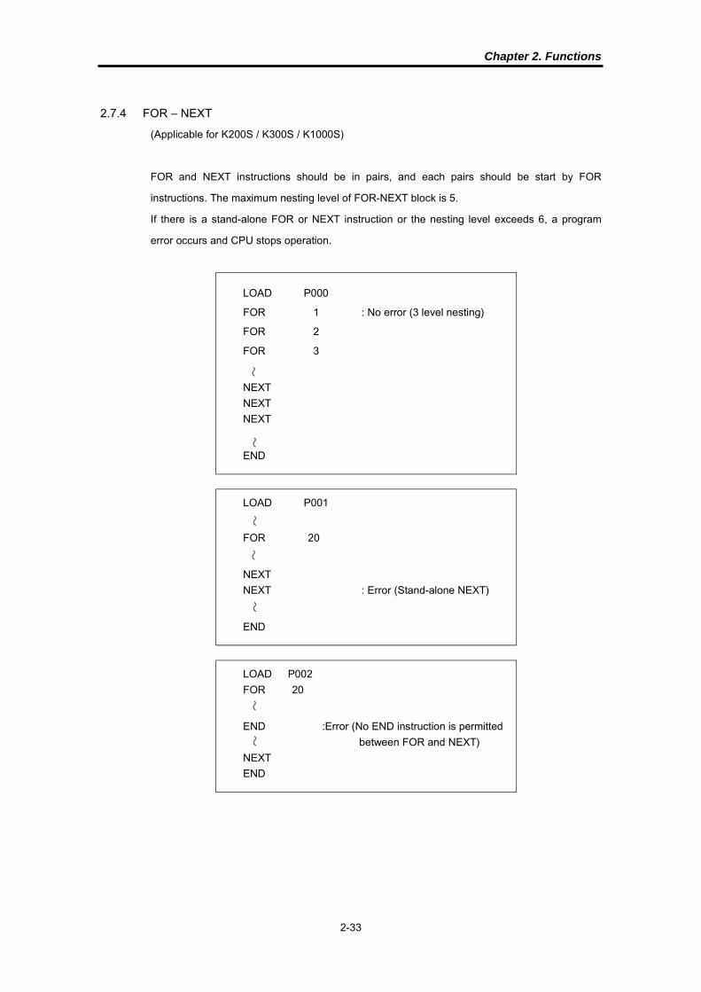
2.7.4 FOR – NEXT
(Applicable for K200S / K300S / K1000S)
FOR and NEXT instructions should be in pairs, and each pairs should be start by FOR
instructions. The maximum nesting level of FOR-NEXT block is 5.
If there is a stand-alone FOR or NEXT instruction or the nesting level exceeds 6, a program
error occurs and CPU stops operation.
LOAD P000
FOR 1 : No error (3 level nesting)
FOR 2
FOR 3
NEXT
NEXT
NEXT
END
LOAD P001
FOR 20
NEXT
NEXT : Error (Stand-alone NEXT)
END
LOAD P002
FOR 20
END :Error (No END instruction is permitted
between FOR and NEXT)
NEXT
END

Chapter 2. Functions
2-34
2.7.5 END / RET
1) If there is no END in a sequence program, a program error occurs and CPU stops operation.
LOAD P012
JMP 10
JME 10
2) If there is no RET in a subroutine program, a program error occurs and CPU stops operation.
END
SBRT
LOAD P000
OUT P010
2.7.6 Dual coil
If a memory device is used as an output of operation two or more times, a dual coil error occurs.
Because this is not a serious error, it does not make the CPU stop.
LOAD P0000
OUT M000
OUT M000 : Dual coil error SET M000 : Dual coil error
: Missing END
: Missing RET

Chapter 2. Functions
2-35
2.8 Error handling
2.8.1 RUN / STOP at operation error
When an operation error (indirect addressing error, BCD operation error, etc) occurs, the CPU
decide to continue operation or not based on parameter setting.
Refer the chapter 2.4.4 for details.
2.8.2 Error flags (F110 / F115)
If an error occurs while the CPU is running, 2 error flags (F110 and F115) are switched on.
The F110 is updated after each instruction is executed. However, the executed instruction is not
related to any error (such as the LOAD instruction), it keeps the previous value. In other hand,
the F115 keeps the on status after it was switched on at once. To clear the F115 flag, execute
the CLE instruction. The following table shows an example of F110 and F115 operation.
Program Error occurred? F110 F115 Remarks
ADD D0 10 M20 No OFF OFF
MOV D0 #D10 Yes ON ON D10 = hFFFF
LOAD P0000 N/A ON ON
INC D0 No OFF ON
LOAD P0001 N/A OFF ON
WAND P01 M10 #D400 Yes ON ON D400 = hFF00
LOAD P0002 N/A ON ON
WAND P01 M10 D300 No OFF ON
CLE N/A OFF OFF Clear F115
LOAD P0003 N/A OFF OFF
WAND P01 M10 D500 No OFF OFF
BCD hFFFF D20 Yes ON ON
Chapter 2. Functions
2-36
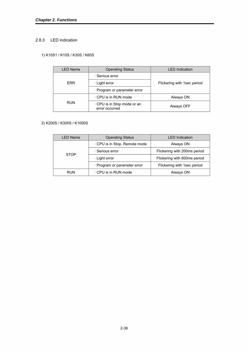
2.8.3 LED indication
1) K10S1 / K10S / K30S / K60S
LED Name Operating Status LED Indication
∙ Serious error
∙ Light errorERR
∙ Program or parameter error
Flickering with 1sec period
∙ CPU is in RUN mode Always ON
RUN ∙ CPU is in Stop mode or an error occurred
Always OFF
2) K200S / K300S / K1000S
LED Name Operating Status LED Indication
∙ CPU is in Stop, Remote mode Always ON
∙ Serious error Flickering with 200ms period
∙ Light error Flickering with 600ms periodSTOP
∙ Program or parameter error Flickering with 1sec period
RUN ∙ CPU is in RUN mode Always ON

Chapter 2. Functions
2-37
2.8.4 Error code list
Error type MessageCode(F006)
CPU Description Corrective action
Internalsystem error
System error h0001 StopThe operating system ROM or otherH/W is defective.
Contact the nearestLG representative
OS ROMerror
OS ROMerror
h0002 Stop The internal system ROM is defective.Contact the nearestLG representative
OS RAMerror
OS RAMerror
h0003 Stop The internal system RAM is defective.Contact the nearestLG representative
Data RAMError
Data RAMerror
h0004 StopThe RAM at which a data is stored isdefective.
Contact the nearestLG representative
ProgramRAM error
Error h0005 StopThe RAM at which a program isstored is defective.
Contact the nearestLG representative
Gate arrayerror
G/A error h0006 Stop The gate array of CPU is defective.Contact the nearestLG representative
Sub rackpower downerror
Sub powererror
h0007 StopThe expansion rack is power off ordefective.
Check the expansionrack is powered.
OS WDTtime out error
OS WDTerror
h0008 StopThe CPU operation time (not the scantime) is too long.
Power off and restartthe CPU. If error stilloccurs, contact thenearest LGrepresentative
Shared RAMerror
CommonRAM error
h0009 Stop Shared RAM interface errorContact the nearestLG representative
Fuse breakerror
I/O fuse error h000ARun
(Stop)The fuse used in output module isblown.
Check the fuse andreplace it.
Instructioncode error
OP codeerror
h000B StopCPU meets an instruction can not bedecoded during executing program.
Contact the nearestLG representative
FlashMemory error
User memoryerror
H000C StopCPU can not access the internal flashmemory
Check the flashmemory and replace itif necessary.
I/O slot error I/O slot error h0010 Stop
① Mount or dismount a module whilethe PLC is powered. A module ismounted improperly.② I/O module or expansion cable isdefective.
① Power off -Remount module –Power on
② Replace the I/Omodule or expansioncable
Maximum I/Oover
Max I/O over h0011 StopI/O points exceed the maximum limitpoints (Fmm mounting numbers overerror, ∙∙∙)
Replace I/O unit
Special CardI/F error
Special I/Ferror
h0012 StopError occurred during special cardinterface
Contact the nearestLG representative
Fmm 0 I/Ferror
Fmm 0 I/Ferror
h0013 Stop Fmm 0 I/F errorContact the nearestLG representative
Fmm 1 I/Ferror
Fmm 1 I/Ferror
h0014 Stop Fmm 1 I/F errorContact the nearestLG representative
Fmm 2 I/Ferror
Fmm 2 I/Ferror
h0015 Stop Fmm 2 I/F errorContact the nearestLG representative
Fmm 3 I/Ferror
Fmm 3 I/Ferror
h0016 Stop Fmm 3 I/F errorContact the nearestLG representative
Parametererror
Parametererror
h0020 StopWhen the parameter is wrong or hasincorrect checksum.
Change parametersetting

Chapter 2. Functions
2-38
Error Code (Continued)
Error type MessageCode(F006)
CPU Description Corrective action
I/O parametererror
I/O parameter error h0021 StopWhen the CPU is powered on or turned toRUN mode, I/O modules are not mountedas I/O reservation of parameter setting.
Change parametersetting or re-arrangeI/O modules
MaximumI/O error
I/O parametererror
h0022 StopI/O parameter setting value or actuallymounted I/O points exceeds themaximum I/O points of CPU module.
Change parametersetting
Fmm 0parametererror
Fmm 0parameter error
h0023 Run Fmm 0 parameter errorChange parametersetting
Fmm 1parametererror
Fmm 1parameter error
h0024 Run Fmm 1 parameter errorChange parametersetting
Fmm 2parametererror
Fmm 2parameter error
h0025 Run Fmm 2 parameter errorChange parametersetting
Fmm 3parametererror
Fmm 3parameter error
h0026 Run Fmm 3 parameter errorChange parametersetting
Operationerror
Operation error h0030Stop(Run)
∙ BCD operation error∙ Operand error
Revise program
WDT error WDT over error h0031 StopThe scan time exceeds the parameter settingvalue of watch dog timer.
Change parametervalue or insert WDTinstruction
Programchange error
PGM Changeerror
h0032 StopAn error occurred while editing programin RUN mode. (The change is notcompleted)
-
Programchange error
PGM Changeerror
h0033 RunA code error occurred while editingprogram in RUN mode.
-
Code checkerror
Code chackerror
h0040 StopThere is an instruction connot bedecoded in program.
Revise program
Missing ENDinstruction
Missing ENDinstruction
h0041 Stop There is no END instruction in program.Insert END instructionat the end of program.
MissingRET error
MissingRET instruction
h0042 Stop There is no RET instruction in subroutine.Insert RET instructionat the end ofsubroutine
MissingSBRT error
MissingSBRT instruction
h0043 StopA subroutine is called with CALLinstruction, but there is no correspongingsubroutine.
Write subroutine.
JMP~JMEinstructionerror
JMP/JMEerror
h0044 StopJMP~JME instructions are usedimproperly in program.
Revise program
FOR~NEXTinstructionerror
FOR~NEXTerror
h0045 StopFOR~NEXT instructions are usedimproperly in program.
Revise program
MCS ~MCSCLRerror
MCS ~MCSCLR error
h0046 StopMCS~MCSCLR instructions are usedimproperly in program.
Revise program
MPUSH ~MPOP error
MPUSH ~MPOP error
h0047 StopMPUSH~MPOP instruction are usedimproperly in program.
Revise program
Dual Coilerror
Dual Coil error h0048 StopA device is used as the output ofoperation more than one time.
Revise program
Syntaxerror
Syntaxerror
h0049 StopWrong input conditions or too manyLOAD instructons, etc.
Revise program
Battery error Battery error h0050 Run The voltege of back-up battery is too lowReplace battery withnew one.

Chapter 3 Instructions
3.1 Basic instructions .............................................................................. 3-1
3.1.1 Contact instructions.......................................................... 3-1
3.1.2 Connection instructions.................................................... 3-1
3.1.3 Inversion instruction ......................................................... 3-1
3.1.4 Master control instructions ............................................... 3-2
3.1.5 Output instructions ........................................................... 3-2
3.1.6 Step controller instructions............................................... 3-2
3.1.7 END instruction ................................................................ 3-2
3.1.8 No operation instruction ................................................... 3-3
3.1.9 Timer instructions............................................................. 3-3
3.1.10 Counter instructions ......................................................... 3-4
3.2 Application instructions ..................................................................... 3-5
3.2.1 Data transfer instructions ................................................. 3-5
3.2.2 Conversion instructions.................................................... 3-6
3.2.3 Compare instructions ....................................................... 3-6
3.2.4 Increment / Decrement instructions.................................. 3-9
3.2.5 Rotation instructions......................................................... 3-9
3.2.6 Shift instructions............................................................. 3-10
3.2.7 Exchange instructions .....................................................3-11
3.2.8 BIN arithmetic instructions ..............................................3-11
3.2.9 BCD arithmetic instructions............................................ 3-13
3.2.10 Logical opration instructions........................................... 3-14
3.2.11 Data processing instructions .......................................... 3-15
3.2.12 System instructions ........................................................ 3-17
3.2.13 Branch instructions......................................................... 3-17
3.2.14 Loop instructions ............................................................ 3-17

3.2.15 Flag instructions ............................................................. 3-18
3.2.16 Special module instructions ........................................... 3-18
3.2.17 Data link instructions ...................................................... 3-18
3.2.18 Interrupt instructions....................................................... 3-19
3.2.19 Sign inversion instructrions ............................................ 3-19
3.2.20 Bit contact instructions ................................................... 3-20
Chapter 3. Instructions
3-1
3 Instructions
3.1 Basic instructions
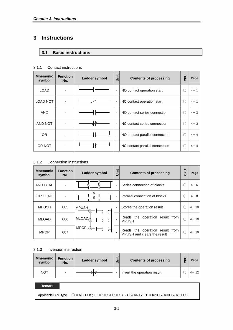
3.1.1 Contact instructions
Mnemonicsymbol
FunctionNo.
Ladder symbol Un
it
Contents of processing
CP
U
Page
LOAD - - NO contact operation start � 4� 1
LOAD NOT - - NC contact operation start � 4� 1
AND - - NO contact series connection � 4� 3
AND NOT - - NC contact series connection � 4� 3
OR - - NO contact parallel connection � 4� 4
OR NOT - - NC contact parallel connection � 4� 4
3.1.2 Connection instructions
Mnemonicsymbol
FunctionNo.
Ladder symbol Un
it
Contents of processing
CP
U
Page
AND LOAD - - Series connection of blocks � 4� 6
OR LOAD - - Parallel connection of blocks � 4� 8
MPUSH 005 - Stores the operation result � 4� 10
MLOAD 006 -Reads the operation result fromMPUSH
� 4� 10
MPOP 007
( )
( )
( )-
Reads the operation result fromMPUSH and clears the result
� 4� 10
3.1.3 Inversion instruction
Mnemonicsymbol
FunctionNo.
Ladder symbol Un
it
Contents of processing
CP
U
Page
NOT - - Invert the operation result � 4� 12
A B
AB
MPUSH
MLOAD
MPOP
Applicable CPU type : � = All CPUs ; � = K10S1 / K10S / K30S / K60S ; � = K200S / K300S / K1000S
Remark

Chapter 3. Instructions
3-2
3.1.4 Master control instructions
Mnemonicsymbol
FunctionNo.
Ladder symbol Un
it
Contents of processing
CP
U
Page
MCS 010 - Start a master control � 4� 13
MCSCLR 011 - End a master control � 4 – 13
3.1.5 Output instructions
Mnemonicsymbol
FunctionNo.
Ladder symbol Un
it
Contents of processing
CP
U
Page
D 017 -Generates one scan pulse on therising edge of input signal.
� 4� 16
D NOT 018 -Generates one scan pulse on thefalling edge of input signal.
� 4 – 18
SET - - Set a device � 4 – 19
RST - - Reset a device � 4 – 20
OUT - ( ) - Output a device �
3.1.6 Step controller instructions
Mnemonicsymbol
FunctionNo.
Ladder symbol Un
it
Contents of processingC
PU
Page
SET S - - Sequential processing control � 4� 22
OUT S - ( Sxx.xx ) - Last-in priority control � 4 – 24
3.1.7 END instruction
Mnemonicsymbol
FunctionNo.
Ladder symbol Un
it
Contents of processing
CP
U
Page
END 001 - Ends a sequence program � 4� 25
MCS n
MCSCLR n
D D
D NOT D
SET D
RST D
SET Sxx.xx
END

Chapter 3. Instructions
3-3
3.1.8 No operation instruction
Mnemonicsymbol
FunctionNo.
Ladder symbol Un
it
Contents of processing
CP
U
Page
NOP 000 No ladder symbol - No operation (occupies 1 step) � 4� 26
3.1.9 Timer instructions
Mnemonicsymbol
FunctionNo.
Ladder symbol Un
it
Contents of processing
CP
U
Page
TON - - � 4� 27
TOFF - - � 4 – 29
TMR - - 4 – 31
TMON - - 4 – 33
TRTG - - 4 – 35
t
Input
Output
t = setting value
<On delay timer>
Timer setting value
TOFF Txxx v
Timer relay No.
Timer setting value
TON Txxx v
Timer relay No.
t
t = setting value
<Off delay timer>
←←←←t1→→→→ ←←←←t 2→→→→
t = setting value ( t = t1+t2 )
<Accumulation timer>
Input
Output
Timer setting value
TMR Txxx v
Timer relay No.
Timer setting value
TMON
Timer relay No.
Txxx v
Timer setting value
Timer relay No.
TRTG Txxx v
t
t
Input
Output
Output
Input
t = setting value
<Monostable timer>
t = setting value
<Retriggerable timer>
Output
Input
Chapter 3. Instructions
3-4
3.1.10 Counter instructions
Mnemonicsymbol
FunctionNo.
Ladder symbol Un
it
Contents of processing
CP
U
Page
CTU - - � 4� 37
CTD - - � 4 – 38
CTUD - � 4 – 39
CTR - � 4 – 41
U CTU
R <S>
CountPulse
Reset
↓
↑Setting value
Counter relay No.
C xxx
v
Reset
CountPulse
Currentvalue
Output
Settingvalue
D CTD
R <S>
CountPulse
Reset
↓
↑Setting value
Counter relay No.
C xxx
v
Reset
CountPulse
Currentvalue
Output
Settingvalue
Reset
UpPulse
Currentvalue
Output
DownPulse
Settingvalue
U CTUD
R <S>
UpPulse
Reset
↓
↑Setting value
Counter relay No.
C xxx
v
D
DownPulse
Output
Reset
CountPulse
Currentvalue
D CTR
R <S>
CountPulse
Reset
↓
↑Setting value
Counter relay No.
C xxx
v
Chapter 3. Instructions
3-5
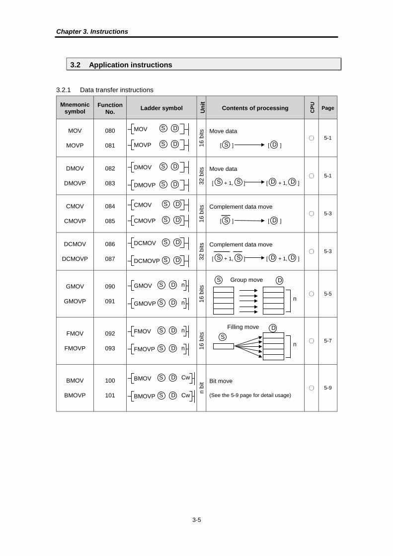
3.2 Application instructions
3.2.1 Data transfer instructions
Mnemonicsymbol
FunctionNo.
Ladder symbol Un
it
Contents of processing
CP
U
Page
MOV
MOVP
080
081 16
bits Move data
[ ] [ ]� 5-1
DMOV
DMOVP
082
083 32
bits Move data
[ + 1, ] [ + 1, ]� 5-1
CMOV
CMOVP
084
085 16
bits Complement data move
[ ] [ ]� 5-3
DCMOV
DCMOVP
086
087 32
bits Complement data move
[ + 1, ] [ + 1, ]� 5-3
GMOV
GMOVP
090
091 16
bits
Group move
� 5-5
FMOV
FMOVP
092
093 16
bits
Filling move
� 5-7
BMOV
BMOVP
100
101
n b
it Bit move
(See the 5-9 page for detail usage)� 5-9
S D
DMOVP S D
MOV S D
MOVP S D
DMOV S D
S DS D
CMOV
CMOVP
DCMOV
S D
S DS DDCMOVP S D
S D
S D
S D
GMOV
GMOVP S D n
S D nS D
n
FMOV
FMOVP S D n
S D nS
D
n
BMOV
BMOVP S D Cw
S D Cw
Chapter 3. Instructions
3-6
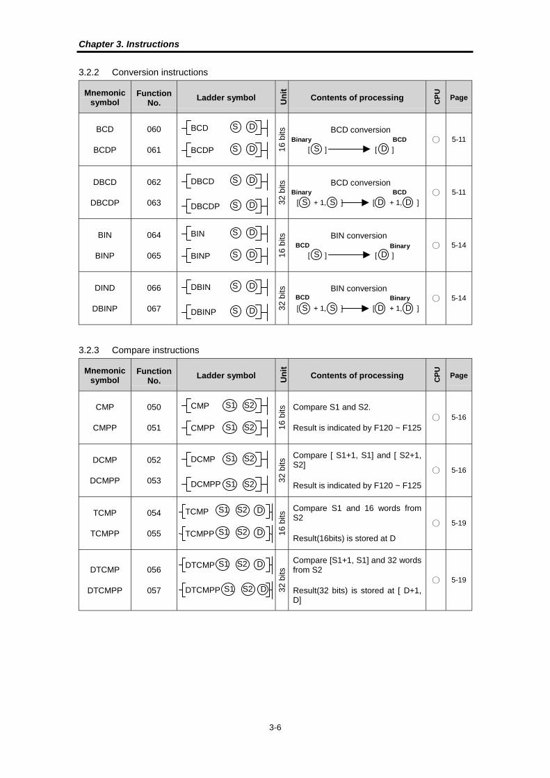
3.2.2 Conversion instructions
Mnemonicsymbol
FunctionNo.
Ladder symbol Un
it
Contents of processing
CP
U
Page
BCD
BCDP
060
061 16
bits BCD conversion
[ ] [ ]� 5-11
DBCD
DBCDP
062
063 32
bits BCD conversion
[ + 1, ] [ + 1, ]� 5-11
BIN
BINP
064
065 16
bits BIN conversion
[ ] [ ]� 5-14
DIND
DBINP
066
067 32
bits BIN conversion
[ + 1, ] [ + 1, ]� 5-14
3.2.3 Compare instructions
Mnemonicsymbol
FunctionNo.
Ladder symbol Un
it
Contents of processing
CP
U
Page
CMP
CMPP
050
051 16
bits Compare S1 and S2.
Result is indicated by F120 ~ F125� 5-16
DCMP
DCMPP
052
053 32
bits
Compare [ S1+1, S1] and [ S2+1,S2]
Result is indicated by F120 ~ F125
� 5-16
TCMP
TCMPP
054
055 16
bits
Compare S1 and 16 words fromS2
Result(16bits) is stored at D
� 5-19
DTCMP
DTCMPP
056
057 32
bits
Compare [S1+1, S1] and 32 wordsfrom S2
Result(32 bits) is stored at [ D+1,D]
� 5-19
S DBinary BCD
BCD
BCDP
S D
S D
DBCD
DBCDP S D
S D
S DS DBinary BCD
S DBCD Binary
BIN
BINP
S D
S D
DBIN
DBINP S D
S D
S DS DBCD Binary
CMP
CMPP
DCMP
DCMPP
TCMP
TCMPP
DTCMP
DTCMPP
S1 S2
S1 S2
S1 S2
S1 S2
S1 S2 D
S1 S2 D
S1 S2 D
S1 S2 D
Chapter 3. Instructions
3-7
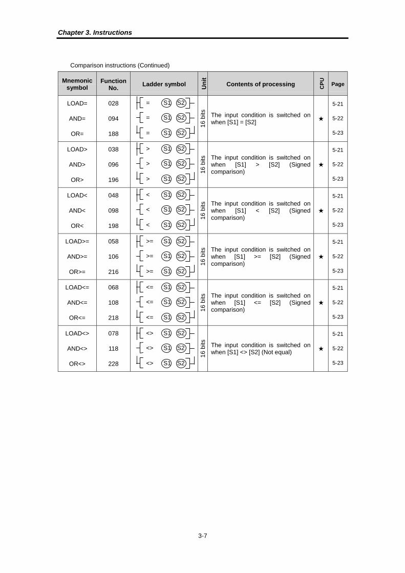
Comparison instructions (Continued)
Mnemonicsymbol
FunctionNo.
Ladder symbol Un
it
Contents of processing
CP
U
Page
LOAD=
AND=
OR=
028
094
188
16
bits The input condition is switched on
when [S1] = [S2]�
5-21
5-22
5-23
LOAD>
AND>
OR>
038
096
196
16
bits The input condition is switched on
when [S1] > [S2] (Signedcomparison)
�
5-21
5-22
5-23
LOAD<
AND<
OR<
048
098
198
16
bits The input condition is switched on
when [S1] < [S2] (Signedcomparison)
�
5-21
5-22
5-23
LOAD>=
AND>=
OR>=
058
106
216
16
bits The input condition is switched on
when [S1] >= [S2] (Signedcomparison)
�
5-21
5-22
5-23
LOAD<=
AND<=
OR<=
068
108
218
16
bits The input condition is switched on
when [S1] <= [S2] (Signedcomparison)
�
5-21
5-22
5-23
LOAD<>
AND<>
OR<>
078
118
228
16
bits The input condition is switched on
when [S1] <> [S2] (Not equal)�
5-21
5-22
5-23
= S1 S2
= S1 S2
= S1 S2
> S1 S2
> S1 S2
> S1 S2
< S1 S2
< S1 S2
< S1 S2
>= S1 S2
>= S1 S2
>= S1 S2
<= S1 S2
<= S1 S2
<= S1 S2
<> S1 S2
<> S1 S2
<> S1 S2
Chapter 3. Instructions
3-8
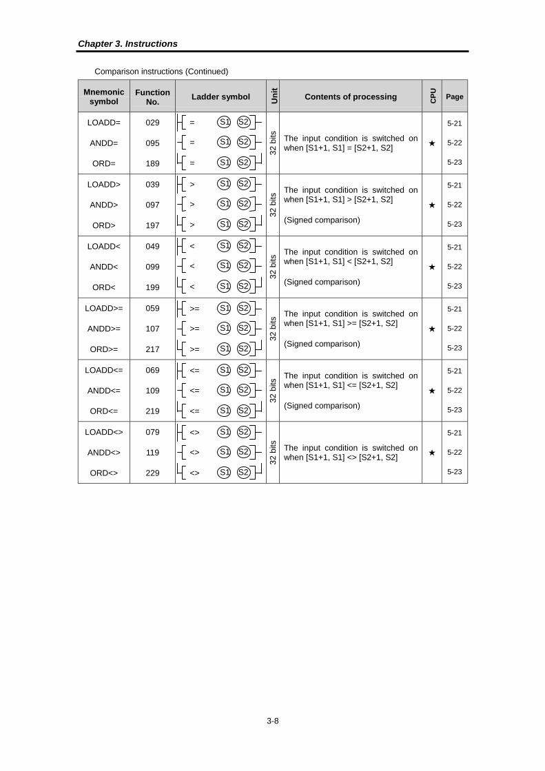
Comparison instructions (Continued)
Mnemonicsymbol
FunctionNo.
Ladder symbol Un
it
Contents of processing
CP
U
Page
LOADD=
ANDD=
ORD=
029
095
189
32
bits The input condition is switched on
when [S1+1, S1] = [S2+1, S2]�
5-21
5-22
5-23
LOADD>
ANDD>
ORD>
039
097
197
32
bits
The input condition is switched onwhen [S1+1, S1] > [S2+1, S2]
(Signed comparison)
�
5-21
5-22
5-23
LOADD<
ANDD<
ORD<
049
099
199
32
bits
The input condition is switched onwhen [S1+1, S1] < [S2+1, S2]
(Signed comparison)
�
5-21
5-22
5-23
LOADD>=
ANDD>=
ORD>=
059
107
217
32
bits
The input condition is switched onwhen [S1+1, S1] >= [S2+1, S2]
(Signed comparison)
�
5-21
5-22
5-23
LOADD<=
ANDD<=
ORD<=
069
109
219
32
bits
The input condition is switched onwhen [S1+1, S1] <= [S2+1, S2]
(Signed comparison)
�
5-21
5-22
5-23
LOADD<>
ANDD<>
ORD<>
079
119
229
32
bits The input condition is switched on
when [S1+1, S1] <> [S2+1, S2]�
5-21
5-22
5-23
= S1 S2
= S1 S2
= S1 S2
> S1 S2
> S1 S2
> S1 S2
< S1 S2
< S1 S2
< S1 S2
>= S1 S2
>= S1 S2
>= S1 S2
<= S1 S2
<= S1 S2
<= S1 S2
<> S1 S2
<> S1 S2
<> S1 S2

Chapter 3. Instructions
3-9
3.2.4 Increment / Decrement instructions
Mnemonicsymbol
FunctionNo.
Ladder symbol Un
it
Contents of processing
CP
U
Page
INC
INCP
020
021 16
bits Increment
[ ] +1 [ ]� 5-24
DINC
DINCP
022
023 32
bits Increment
[ +1, ] +1 [ +1, ]� 5-24
DEC
DECP
024
025 16
bits Decrement
[ ] -1 [ ]� 5-26
DDEC
DDECP
026
027 32
bits Decrement
[ +1, ] -1 [ +1, ]� 5-26
3.2.5 Rotation instructions
Mnemonicsymbol
FunctionNo.
Ladder symbol Un
it
Contents of processing
CP
U
Page
ROL
ROLP
020
021 16
bits
� 5-28
ROR
RORP
034
035 16
bits
5-30
RCL
RCLP
040
041 16
bits
5-32
RCR
RCRP
044
045 16
bits
5-34
INC
INCP
D
D
DINC
DINCP
D
D
DEC
DECP
D
D
DDEC
DDECP
D
D
D D
D DD D
D D
D DD D
ROL
ROLP
D
D
D15 0D15 0
1 bit rotate to left
Carry
ROR
RORP
D
D
RCL
RCLP
D
D
RCR
RCRP
D
D
D15 0D15 0
1 bit rotate to left include carry
Carry
D15 0D15 0 Carry
1 bit rotate to right
D15 0D15 0 Carry
1 bit rotate to right include carry
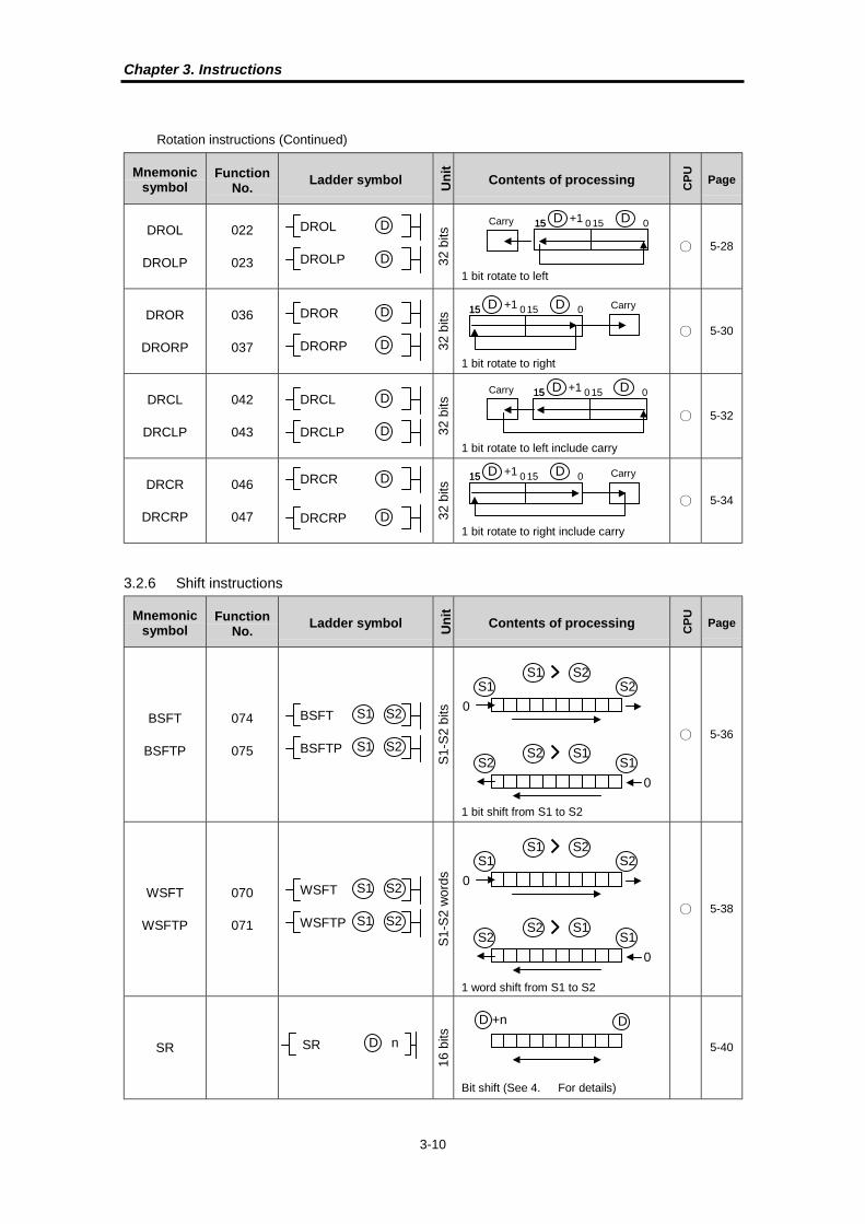
Chapter 3. Instructions
3-10
Rotation instructions (Continued)
Mnemonicsymbol
FunctionNo.
Ladder symbol Un
it
Contents of processing
CP
U
Page
DROL
DROLP
022
023 32
bits
� 5-28
DROR
DRORP
036
037 32
bits
� 5-30
DRCL
DRCLP
042
043 32
bits
� 5-32
DRCR
DRCRP
046
047 32
bits
� 5-34
3.2.6 Shift instructions
Mnemonicsymbol
FunctionNo.
Ladder symbol Un
it
Contents of processing
CP
U
Page
BSFT
BSFTP
074
075
S1
-S2
bits
� 5-36
WSFT
WSFTP
070
071
S1
-S2
wo
rds
� 5-38
SR
16
bits
5-40
DROL
DROLP
D
D
DROR
DRORP
D
D
DRCL
DRCLP
D
D
DRCR
DRCRP
D
D
1 bit rotate to left
Carry
1 bit rotate to left include carry
Carry
Carry
1 bit rotate to right
Carry
1 bit rotate to right include carry
D15 0D15 0 15+1
D15 0D15 0 15+1
D15 0D15 0 15+1
D15 0D15 0 15+1
BSFT
BSFTP
S1 S2
S1 S2
0
S2 S1
0
S1 S2S1 S2
S2 S1
1 bit shift from S1 to S2
WSFT
WSFTP
S1 S2
S1 S2
0
S2 S1
0
S1 S2S1 S2
S2 S1
1 word shift from S1 to S2
SR D n
Bit shift (See 4. For details)
DD +n

Chapter 3. Instructions
3-11
3.2.7 Exchange instructions
Mnemonicsymbol
FunctionNo.
Ladder symbol Un
it
Contents of processing
CP
U
Page
XCH
XCHP
102
103 16
bits
[ D1 ] [ D2 ] � 5-42
DXCH
DXCHP
104
105 32
bits
[ D1+1, D1 ] [ D2+1, D2 ] � 5-42
3.2.8 BIN arithmetic instructions
Mnemonicsymbol
FunctionNo.
Ladder symbol Un
it
Contents of processing
CP
U
Page
ADD
ADDP
110
111 16
bits
[ S1 ] + [ S2 ] [ D ] � 5-44
DADD
DADDP
112
113 32
bits [S1+1, S1] + [S2+1, S2]
[D+1, D]� 5-44
SUB
SUBP
114
115 16
bits
[ S1 ] - [ S2 ] [ D ] � 5-46
DSUB
DSUBP
116
117 32
bits [S1+1, S1] - [S2+1, S2]
[D+1, D]� 5-46
MUL
MULP
120
121 16
bits [ S1 ] � [ S2 ] [ D+1, D ]
[D+1] : High word, [D] : Low word� 5-48
DMUL
DMULP
122
123 32
bits
[S1+1, S1]�[S2+1, S2]
[D+3,D+2,D+1,D]
[D+3,D+2] = Higher 2 words
[D+1, D] = Lower 2 words
� 5-48
XCH
XCHP
D1 D2
D1 D2
DXCH
DXCHP
D1 D2
D1 D2
S1 S2
S1 S2 D
S1 S2 D
ADD
ADDP
D
DADD
DADDP S1 S2 D
S1 S2
S1 S2 D
S1 S2 D
SUB
SUBP
D
DSUB
DSUBP S1 S2 D
S1 S2
S1 S2 D
S1 S2 D
MUL
MULP
D
DMUL
DMULP S1 S2 D

Chapter 3. Instructions
3-12
BIN arithmetic instructions (Continued)
Mnemonicsymbol
FunctionNo.
Ladder symbol Un
it
Contents of processing
CP
U
Page
DIV
DIVP
124
125 16
bits
[ S1 ]�[ S2 ] [ D ]
[D+1] = Remainder
[D] = Quotient
� 5-50
DDIV
DDIVP
126
127 32
bits
[S1+1, S1]�[S2+1, S2]
[D+3, D+2, D+1, D]
[D+3, D+2] = Remainder
[D+1, D] = Quotient
� 5-50
MULS
MULSP
072
073 16
bits
Signed multiplying operation
[ S1 ] � [ S2 ] [ D+1, D ]
[D+1] : High word, [D] : Low word
�
DMULS
DMULSP
076
077 32
bits
Signed multiplying operation
[S1+1, S1]�[S2+1, S2]
[D+3,D+2,D+1,D]
[D+3,D+2] = Higher 2 words
[D+1, D] = Lower 2 words
�
DIVS
DIVSP
088
089 16
bits
Signed dividing operation
[ S1 ]�[ S2 ] [ D ]
[D+1] = Remainder
[D] = Quotient
�
DDIVS
DDIVSP
128
129 32
bits
Signed dividing operation
[S1+1, S1]�[S2+1, S2]
[D+3, D+2, D+1, D]
[D+3, D+2] = Remainder
[D+1, D] = Quotient
�
S1 S2
S1 S2 D
S1 S2 D
DIV
DIVP
D
DDIV
DDIVP S1 S2 D
S1 S2
S1 S2 D
MULS
MULSP
D
S1 S2 DDMULS
DMULSP S1 S2 D
S1 S2
S1 S2 D
DIVS
DIVSP
D
S1 S2 DDDIVS
DDIVSP S1 S2 D

Chapter 3. Instructions
3-13
3.2.9 BCD arithmetic instructions
Mnemonicsymbol
FunctionNo.
Ladder symbol Un
it
Contents of processing
CP
U
Page
ADDB
ADDBP
130
131 16
bits BCD addition
[ S1 ] + [ S2 ] [ D ]� 5-52
DADDB
DADDBP
132
133 32
bits BCD addition
[S1+1,S1]+[S2+1,S2] [D+1,D]� 5-52
SUBB
SUBBP
134
135 16
bits BCD subtraction
[ S1 ] - [ S2 ] [ D ]� 5-54
DSUBB
DSUBBP
136
137 32
bits BCD subtraction
[S1+1,S1]-[S2+1,S2] [D+1,D]� 5-54
MULB
MULBP
140
141 16
bits
BCD multiplication
[ S1 ] � [ S2 ] [ D+1, D ]
[D+1] : High word, [D] : Low word
� 5-56
DMULB
DMULBP
142
143 32
bits
BCD multiplication
[S1+1, S1]�[S2+1, S2]
[D+3,D+2,D+1,D]
[D+3,D+2] = Higher 2 words
[D+1, D] = Lower 2 words
� 5-56
DIVB
DIVBP
144
145 16
bits
BCD division
[ S1 ]�[ S2 ] [ D ]
[D+1] = Remainder
[D] = Quotient
� 5-58
DDIVB
DDIVBP
146
147 32
bits
BCD division
[S1+1, S1]�[S2+1, S2]
[D+3, D+2, D+1, D]
[D+3, D+2] = Remainder
[D+1, D] = Quotient
� 5-58
S1 S2 DDMULB
DMULBP S1 S2 D
S1 S2
S1 S2 D
DIVB
DIVBP
D
S1 S2 DDDIVB
DDIVBP S1 S2 D
S1 S2
S1 S2 D
MULB
MULBP
D
S1 S2
S1 S2 D
ADDB
ADDBP
D
S1 S2 DDADDB
DADDBP S1 S2 D
S1 S2
S1 S2 D
SUBB
SUBBP
D
S1 S2 DDSUBB
DSUBBP S1 S2 D

Chapter 3. Instructions
3-14
3.2.10 Logical opration instructions
Mnemonicsymbol
FunctionNo.
Ladder symbol Un
it
Contents of processing
CP
U
Page
WAND
WANDP
130
131 16
bits
[ S1 ] AND [ S2 ] [ D ] � 5-60
DWAND
DWANDP
132
133 32
bits [S1+1,S1] AND [S2+1,S2]
[D+1,D]� 5-60
WOR
WORP
154
155 16
bits
[ S1 ] OR [ S2 ] [ D ] � 5-62
DWOR
DWORP
156
157 32
bits [S1+1,S1] OR [S2+1,S2]
[D+1,D]� 5-62
WXOR
WXORP
160
161 16
bits
[ S1 ] XOR [ S2 ] [ D ] � 5-64
DWXOR
DWXORP
162
163 32
bits [S1+1,S1] XOR [S2+1,S2]
[D+1,D]� 5-64
WXNR
WXNRP
164
165 [ S1 ] XNR [ S2 ] [ D ] 5-66
DWXNR
DWXNRP
166
167
[S1+1,S1] XNR [S2+1,S2]
[D+1,D]5-66
S1 S2
S1 S2 D
WAND
WANDP
D
S1 S2 DDWAND
DWANDP S1 S2 D
S1 S2
S1 S2 D
WAND
WANDP
D
S1 S2 DDWAND
DWANDP S1 S2 D
S1 S2
S1 S2 D
WXOR
WXORP
D
S1 S2 DDWXOR
DWXORP S1 S2 D
S1 S2
S1 S2 D
WXNR
WXNRP
D
S1 S2 DDWXNR
DWXNRP S1 S2 D
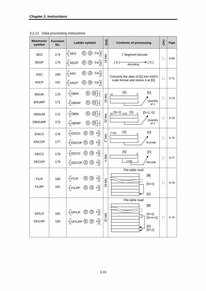
Chapter 3. Instructions
3-15
3.2.11 Data processing instructions
Mnemonicsymbol
FunctionNo.
Ladder symbol Un
it
Contents of processing
CP
U
Page
SEG
SEGP
174
175 16
bits 7 Segment decode
[ S ] [ D ]� 5-68
ASC
ASCP
190
191
Converts the data of [S] into ASCIIcode format and stores it at [D].
� 5-71
BSUM
BSUMP
170
171 16
bits
� 5-73
DBSUM
DBSUMP
172
173 32
bits
� 5-73
ENCO
ENCOP
176
177 2n b
its
� 5-75
DECO
DECOP
178
179 n b
its
� 5-77
FILR
FILRP
180
181 16
bits
� 5-79
DFILR
DFILRP
182
183 32
bits
� 5-79
SEG
SEGP S D Cw
S D Cw
decoding
ASC
ASCP S D Cw
S D Cw
DBIN
DBINP S D
S D 15 0
Quantityof 1
DBIN
DBINP S D
S D 15 0[S]
Quantityof 1
015[S+1]
[S]
[D+1, D]
[D]
ENCO
ENCOP S D n
S D n
DECO
DECOP S D n
S D n
2n bits 0
Encode
[S] [D]
n bits
0
Decode
[S] [D]
FILR
FILRP S D n
S D n[S][S]
[S+n]
[D]
File table read
DFILR
DFILRP S D n
S D n
[S][S]
[S+n][S+n+1]
[D][D+1]
File table read

Chapter 3. Instructions
3-16
Data processing instructions (Continued)
Mnemonicsymbol
FunctionNo.
Ladder symbol Un
it
Contents of processing
CP
U
Page
FILW
FILWP
184
185 16
bits
� 5-81
DFILW
DFILWP
186
187 32
bits
� 5-81
DIS
DISP
194
195 16
bits
� 5-83
UNI
UNIP
192
193 32
bits
� 5-85
IORF
IORFP
200
201 16
bits Refreshes the memory area
from[D1] to [D2] ( [D1] < [D2] )� 5-87
FILW
FILWP S D n
S D n[S][S]
[S+n]
[D]
File table write
[S][S]
File table write
DFILW
DFILWP S D n
S D n[S+n][S+n+1]
[D][D+1]
4bits
4bits
[S]
[D][D+1][D+2]
All 0
Whenn=3
DIS
DISP S D n
S D n
[S][S+1][S+2]
4bits
4bits
[D]Whenn=3
UNI
UNIP S D n
S D n
IORF
IORFP
D1 D2
D1 D2
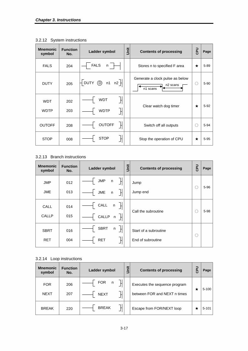
Chapter 3. Instructions
3-17
3.2.12 System instructions
Mnemonicsymbol
FunctionNo.
Ladder symbol Un
it
Contents of processing
CP
U
Page
FALS 204 Stores n to specified F area � 5-89
DUTY 205
Generate a clock pulse as below� 5-90
WDT
WDTP
202
203Clear watch dog timer � 5-92
OUTOFF 208 Switch off all outputs � 5-94
STOP 008 Stop the operation of CPU � 5-95
3.2.13 Branch instructions
Mnemonicsymbol
FunctionNo.
Ladder symbol Un
it
Contents of processing
CP
U
Page
JMP
JME
012
013
Jump
Jump end� 5-96
CALL
CALLP
014
015Call the subroutine � 5-98
SBRT
RET
016
004
Start of a subroutine
End of subroutine�
3.2.14 Loop instructions
Mnemonicsymbol
FunctionNo.
Ladder symbol Un
it
Contents of processing
CP
U
Page
FOR
NEXT
206
207
Executes the sequence program
between FOR and NEXT n times� 5-100
BREAK 220 Escape from FOR/NEXT loop � 5-101
FALS n
DUTY D n1 n2
n1 scansn2 scans
WDT
WDTP
OUTOFF
STOP
JMP n
JME n
CALL n
CALLP n
SBRT n
RET
NEXT
FOR n
BREAK

Chapter 3. Instructions
3-18
3.2.15 Flag instructions
Mnemonicsymbol
FunctionNo.
Ladder symbol Un
it
Contents of processing
CP
U
Page
STC
CLC
002
003
Set the carry flag
Clear the carry flag� 5-102
CLE 009 Clear the error flag � 5-103
3.2.16 Special module instructions
Mnemonicsymbol
FunctionNo.
Ladder symbol Un
it
Contents of processing
CP
U
Page
GET
GETP
230
231
Read data from shared RAM of
a special module� 5-104
PUT
PUTP
234
235
Write data to shared RAM of
a special module� 5-106
3.2.17 Data link instructions
Mnemonicsymbol
FunctionNo.
Ladder symbol Un
it
Contents of processingC
PU
Page
READ
WRITE
244
245
Read /Write data of remote
station�
5-108
5-111
RGET
RPUT
232
233
Read / Write data of shared
RAM of remote special module�
5-113
5-116
CONN 246Establish a communicationchannel
�
STATUS 247Read the information of remotestation
� 5-118
CLC
STC
CLE
S D
S Dn1 n2
GET n1 n2
GETP
S D
S Dn1 n2
PUT n1 n2
PUTP
READ n1 st n SSSD
n1 st n SSSDWRITE
RGET n1 st n SSSD
n1 st n SSSDRPUT
n1 st SSDCONN
n1 st SSDSTATUS
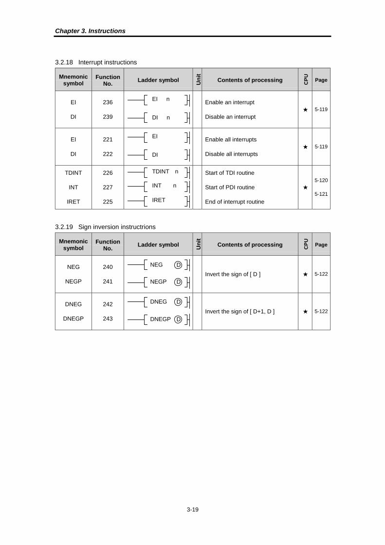
Chapter 3. Instructions
3-19
3.2.18 Interrupt instructions
Mnemonicsymbol
FunctionNo.
Ladder symbol Un
it
Contents of processing
CP
U
Page
EI
DI
236
239
Enable an interrupt
Disable an interrupt� 5-119
EI
DI
221
222
Enable all interrupts
Disable all interrupts� 5-119
TDINT
INT
IRET
226
227
225
Start of TDI routine
Start of PDI routine
End of interrupt routine
�
5-120
5-121
3.2.19 Sign inversion instructrions
Mnemonicsymbol
FunctionNo.
Ladder symbol Un
it
Contents of processing
CP
U
Page
NEG
NEGP
240
241Invert the sign of [ D ] � 5-122
DNEG
DNEGP
242
243Invert the sign of [ D+1, D ] � 5-122
DI n
EI n
DI
EI
TDINT n
INT n
IRET
NEG D
NEGP D
DNEG D
DNEGP D

Chapter 3. Instructions
3-20
3.2.20 Bit contact instructions
Mnemonicsymbol
FunctionNo.
Ladder symbol Un
it
Contents of processing
CP
U
Page
BLD 248 -NO contact operation start with thenth bit of [ D ]
� 5-124
BLDN 249NC contact operation start with thenth bit of [ D ]
� 5-124
BAND 250NO contact series connection withthe nth bit of [ D ]
� 5-125
BANDN 251NC contact series connection withthe nth bit of [ D ]
� 5-125
BOR 252NO contact parallel connection withthe nth bit of [ D ]
� 5-126
BORN 253NC contact parallel connection withthe nth bit of [ D ]
� 5-126
BOUT 236Output the result of operation to thenth bit of [ D ]
� 5-127
BSET 223 Set the nth bit of [ D ] � 5-128
BRST 224 Clear the nth bit of [ D ] � 5-128
B D n
BN D n
B D n
BN D n
B D n
BN D n
BOUT D n
SET D n
RST D n

Chapter 4 Basic instructions
4.1 Contact instructions .......................................................................... 4-1
4.1.1 LOAD, LOAD NOT, OUT.................................................. 4-1
4.1.2 AND, AND NOT ............................................................... 4-3
4.1.3 OR, OR NOT.................................................................... 4-4
4.2 Connection instructions..................................................................... 4-6
4.2.1 AND LOAD....................................................................... 4-6
4.2.2 OR LOAD......................................................................... 4-8
4.2.3 MPUSH, MLOAD, MPOP............................................... 4-10
4.3 Inversion instruction ........................................................................ 4-12
4.3.1 NOT................................................................................ 4-12
4.4 Master control instructions .............................................................. 4-13
4.4.1 MCS, MCSCLR .............................................................. 4-13
4.5 Output instructions .......................................................................... 4-16
4.5.1 OUT................................................................................ 4-16
4.5.2 D .................................................................................... 4-17
4.5.3 D NOT............................................................................ 4-19
4.5.4 SET ................................................................................ 4-20
4.5.5 RST................................................................................ 4-21
4.6 Step controller instructions.............................................................. 4-23
4.6.1 SET Sxx.xx..................................................................... 4-23
4.6.2 OUT Sxx.xx .................................................................... 4-25
4.7 End instructions .............................................................................. 4-26
4.7.1 END ............................................................................... 4-26
4.8 No operation instruction .................................................................. 4-27
4.8.1 NOP ............................................................................... 4-27
4.9 Timer instructions............................................................................ 4-28
4.9.1 TON................................................................................ 4-28
4.9.2 TOFF.............................................................................. 4-30

4.9.3 TMR ............................................................................... 4-32
4.9.4 TMON............................................................................. 4-34
4.9.5 TRTG ............................................................................. 4-36
4.10 Counter instructions ........................................................................ 4-38
4.10.1 CTU................................................................................ 4-38
4.10.2 CTD................................................................................ 4-39
4.10.3 CTUD ............................................................................. 4-40
4.10.4 CTR................................................................................ 4-42
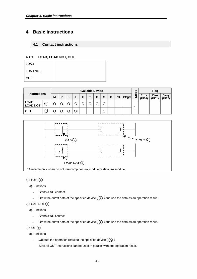
Chapter 4. Basic instructions
4-1
4 Basic instructions
4.1 Contact instructions
4.1.1 LOAD, LOAD NOT, OUT
LOAD
LOAD NOT
OUT
Available Device FlagInstructions
M P K L F T C S D #D Integer Ste
ps
Error(F110)
Zero(F111)
Carry(F112)
LOADLOAD NOT O O O O O O O O
OUT D O O O O* O1
* Available only when do not use computer link module or data link module
1) LOAD
a) Functions
� Starts a NO contact.
� Draw the on/off data of the specified device ( ) and use the data as an operation result.
2) LOAD NOT
a) Functions
� Starts a NC contact.
� Draw the on/off data of the specified device ( ) and use the data as an operation result.
3) OUT
a) Functions
� Outputs the operation result to the specified device ( ).
� Several OUT instructions can be used in parallel with one operation result.
LOAD OUT
LOAD NOT
S
S
D
S
S
S
S
S
D
D
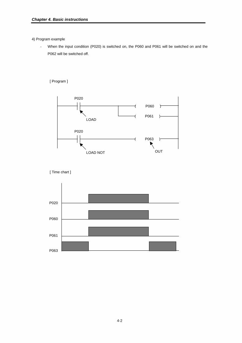
Chapter 4. Basic instructions
4-2
OUT
4) Program example
� When the input condition (P020) is switched on, the P060 and P061 will be switched on and the
P062 will be switched off.
LOAD
P020
( P060 )
LOAD NOT
P020
( P063 )
( P061 )
P020
P060
P061
P063
[ Program ]
[ Time chart ]
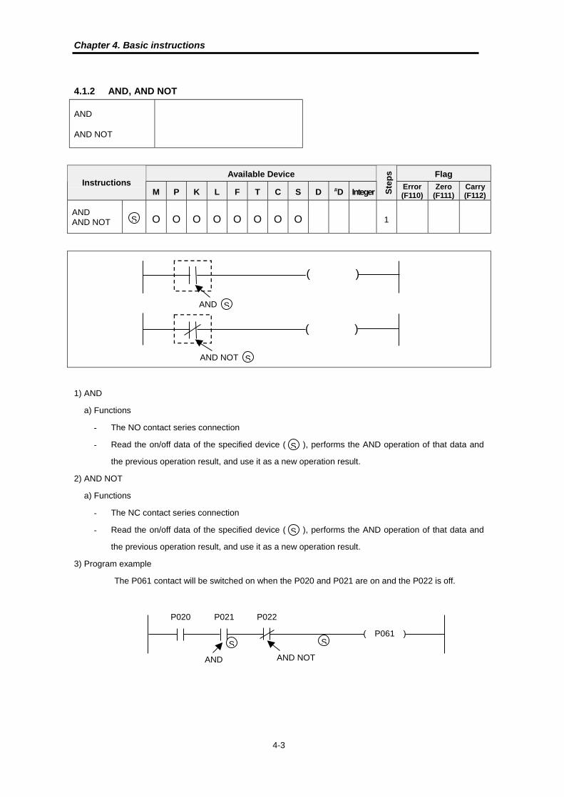
Chapter 4. Basic instructions
4-3
4.1.2 AND, AND NOT
AND
AND NOT
Available Device FlagInstructions
M P K L F T C S D #D Integer Ste
ps
Error(F110)
Zero(F111)
Carry(F112)
ANDAND NOT O O O O O O O O 1
1) AND
a) Functions
� The NO contact series connection
� Read the on/off data of the specified device ( ), performs the AND operation of that data and
the previous operation result, and use it as a new operation result.
2) AND NOT
a) Functions
� The NC contact series connection
� Read the on/off data of the specified device ( ), performs the AND operation of that data and
the previous operation result, and use it as a new operation result.
3) Program example
The P061 contact will be switched on when the P020 and P021 are on and the P022 is off.
S
AND
AND NOT
( )
( )
S
S
S
S
P020
( P061 )
P021 P022
AND AND NOT
S S

Chapter 4. Basic instructions
4-4
4.1.3 OR, OR NOT
OR
OR NOT
Available Device FlagInstructions
M P K L F T C S D #D Integer Ste
ps
Error(F110)
Zero(F111)
Carry(F112)
OROR NOT O O O O O O O O 1
1) OR
a) Functions
� The NO contact parallel connection
� Draw the on/off data of the specified device ( ), performs the OR operation of that data and the
previous operation result, and use it as a new operation result.
2) OR NOT
a) Functions
� The NC contact parallel connection
� Draw the on/off data of the specified device ( ), performs the OR operation of that data and the
previous operation result, and use it as a new operation result.
3) Program example
The P061 contact will switched on when the one of P020 and P021 is on.
S
OR
( )
OR NOT
S
S
S
S
P020( P061 )
P021
OR
S

Chapter 4. Basic instructions
4-5
The motor operation (Example of LOAD, AND, OR, OUT instructions)
1. Operation
There are three push-button switches - PB0, PB1, and PB2. When PB1 is pushed, a motor will start to
rotate with a forward (clockwise) direction. It will start to rotate with a reverse (counterclockwise) direction
when the PB2 is pushed. The PB0 is emergency stop switch and the motor will stop operation when the
PB0 is pushed.
2. System structure
3. Program
0
1
2
3
0
1
2
3
<Stop> PB0
<Forward> PB1
Digital inputmodule[ P03 ]
Digital outputmodule[ P06 ]
<Reverse> PB2
Mag. S/WMag. S/W
M
Forward rotation
Reverse rotation
Motor
( P060 )P031
P060
( P061 )P032
P061
P030 P032 P061
P030 P031 P060
[ END ]
0000
0006
0011
∙ Forward operation, Set an interlockwith reverse operation (P032, P061)
P032 P061
∙ Reverse operation. Set an interlockwith forward operation (P031, P062)
P031 P060
[ Self-locking circuit ]
Once the P031 is switched on, the
P060 will be turned on and it will
keep itself as the on state until the
P030 is switched on.
Remark
P031( P060 )
P060
P030
0000

Chapter 4. Basic instructions
4-6
4.2 Connection instructions
4.2.1 AND LOAD
AND LOAD
Available Device FlagInstructions
M P K L F T C S D #D Integer Ste
ps
Error(F110)
Zero(F111)
Carry(F112)
AND LOAD 1
1) Functions
� Performs the AND operation of block A and block B, and uses it as an operation result.
� The AND LOAD instruction can be written consecutively up to 7 times.
2) Program example
AND LOAD
Block A
( )
Block B
( P060 )P021
P023 P024 P026
P025
P022
P020
AND LOAD
P020
P022
P026
P060
[ Program ]
[ Time chart ]

Chapter 4. Basic instructions
4-7
[ NOTE ] The consecutive use of the AND LOAD instruction
There are two methods to connect several blocks in serial. See the following example.
The AND LOAD instruction can be used consecutively up to 7 times (8 block). When connect more than 9
blocks in serial, write a mnemonic program such as the example [ A ]. If you use KGL-WIN software and
write program in ladder mode, the KGL-WIN software will convert the ladder program into mnemonic
program [ A ] automatically.
( P060 )M000 M002 M004 M006 M008
M001 M003 M004 M007 M009
[ END ]
[ Ladder program ]
[ Mnemonic program ]
LOAD
OR
LOAD
OR
AND LOAD
LOAD
OR
AND LOAD
LOAD
OR
AND LOAD
LOAD
OR
AND LOAD
OUT
END
M000
M001
M002
M003
M004
M005
M006
M007
M008
M009
P060
[ A ] Don’t use AND LOADinstructions consecutively
LOAD
OR
LOAD
OR
LOAD
OR
LOAD
OR
LOAD
OR
AND LOAD
AND LOAD
AND LOAD
AND LOAD
OUT
END
M000
M001
M002
M003
M004
M005
M006
M007
M008
M009
P060
[ B] Use AND LOAD instructionsconsecutively

Chapter 4. Basic instructions
4-8
4.2.2 OR LOAD
OR LOAD
Available Device FlagInstructions
M P K L F T C S D #D Integer Ste
ps
Error(F110)
Zero(F111)
Carry(F112)
OR LOAD 1
1) Functions
� Performs the OR operation of block A and block B, and uses it as an operation result.
� The AND LOAD instruction can be written consecutively up to 7 times.
2) Program example
Block A
( )
Block A
( P060 )P021
P023
P023
P020
OR LOAD
P024
P025
P060
P061
P025
P024
P026
( P061 )
P020
[ Program ]
[ Time chart ]
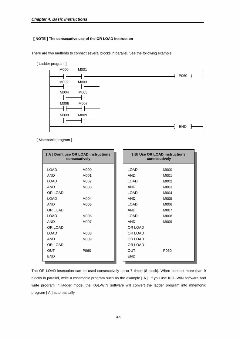
Chapter 4. Basic instructions
4-9
[ NOTE ] The consecutive use of the OR LOAD instruction
There are two methods to connect several blocks in parallel. See the following example.
The OR LOAD instruction can be used consecutively up to 7 times (8 block). When connect more than 9
blocks in parallel, write a mnemonic program such as the example [ A ]. If you use KGL-WIN software and
write program in ladder mode, the KGL-WIN software will convert the ladder program into mnemonic
program [ A ] automatically.
[ Ladder program ]
[ Mnemonic program ]
LOAD
AND
LOAD
AND
OR LOAD
LOAD
AND
OR LOAD
LOAD
AND
OR LOAD
LOAD
AND
OR LOAD
OUT
END
M000
M001
M002
M003
M004
M005
M006
M007
M008
M009
P060
[ A ] Don’t use OR LOAD instructionsconsecutively
LOAD
AND
LOAD
AND
LOAD
AND
LOAD
AND
LOAD
AND
OR LOAD
OR LOAD
OR LOAD
OR LOAD
OUT
END
M000
M001
M002
M003
M004
M005
M006
M007
M008
M009
P060
[ B] Use OR LOAD instructionsconsecutively
( P060 )
M000 M001
M002 M003
[ END ]
M004 M005
M006 M007
M008 M009

Chapter 4. Basic instructions
4-10
4.2.3 MPUSH, MLOAD, MPOP
MPUSH
MLOAD
MPOP
FUN (005) MPUSH
FUN (006) MLOAD
FUN (007) MPOP
Available Device FlagInstructions
M P K L F T C S D #D Integer Ste
ps
Error(F110)
Zero(F111)
Carry(F112)
MPUSHMLOADMPOP
1
1) Functions
a) MPUSH : Stores the operation result (On/Off) immediately preceding the MPUSH instruction.
b) MLOAD : Reads the operation result stored by the MPUSH instruction and resume the operation with
that operation result, starting at the next step.
c) MPOP : Reads the operation result stored by the MPUSH instruction and resumes the operation with
that operation result, starting at the next step. Then clears the operation result stored by the MPUSH
instruction.
d) The MPUSH instruction can be used up to 8 times consecutively. If a MLOAD instruction is used in
between, 1 is reduced from the number of used MPS instructions.
MPUSH
MLOAD
MPOP

Chapter 4. Basic instructions
4-11
2) Program example
P020 P021 P022 P023 P024
P025
[ END ]
( )P060
( )P061
P026( )P062
P027( )P063
P028( )P064
( )P065
P02A( )P066
P029
00000
00027
0000000100020003000400050006000700080009001000110012001300140015001600170018001900200021002200230024002500260027002800290030
STEP INSTRUCTION
LOADMPUSHANDMPUSHANDANDMPUSHANDOUTMLOADANDOUTMPOPANDOUTMLOADANDOUTMPOPANDOUTMLOADANDOUTMPOPANDOUTENDNOPNOPNOP
P020
P021
P022P023
P024P061
P025P061
P026P061
P027P063
P028P064
P029P065
P02AP066
[ Ladder program ]
[ Mnemonic program ]

Chapter 4. Basic instructions
4-12
4.3 Inversion instruction
4.3.1 NOT
NOT
Available Device FlagInstructions
M P K L F T C S D #D Integer Ste
ps
Error(F110)
Zero(F111)
Carry(F112)
NOT 1
1) Functions
� Inverts the operation result before the NOT instruction.
Before NOT instruction After NOT instruction
NC contact NO contact
NO contact NC contact
Serial (AND) connection Parallel (OR) connection
Parallel (OR) connection Serial (AND) connection
2) Program example
The following two programs perform same operation.
( )NOT
Program A
( P060 )
P020 P021 P022 P023 P024
Program B
( P060 )P020
P021
P022
P023
P024
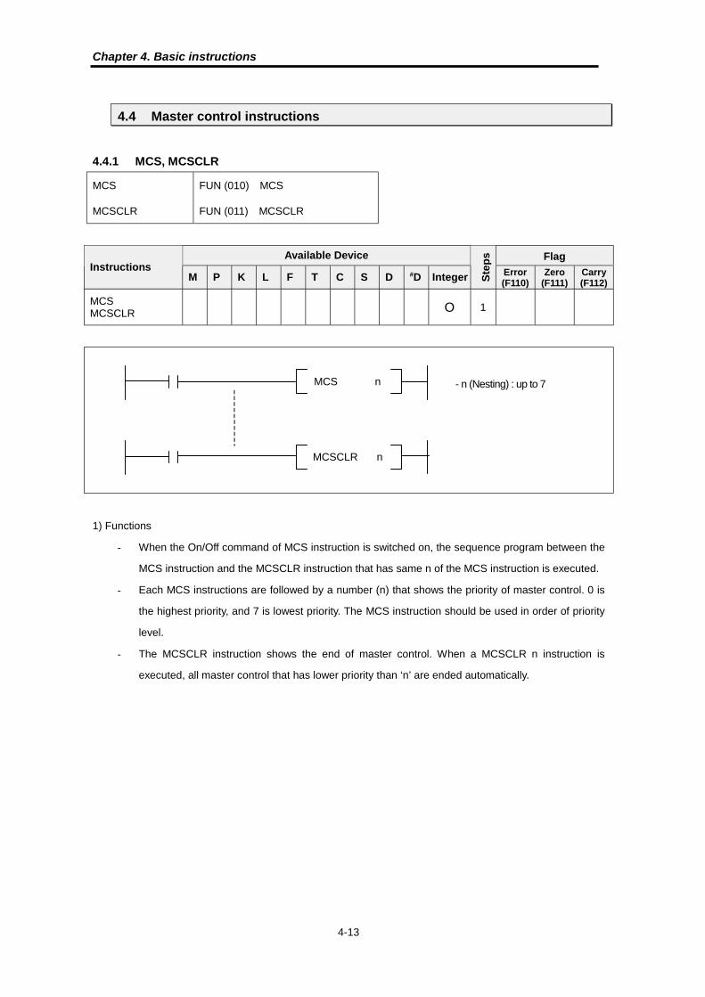
Chapter 4. Basic instructions
4-13
4.4 Master control instructions
4.4.1 MCS, MCSCLR
MCS
MCSCLR
FUN (010) MCS
FUN (011) MCSCLR
Available Device FlagInstructions
M P K L F T C S D #D Integer Ste
ps
Error(F110)
Zero(F111)
Carry(F112)
MCSMCSCLR O 1
1) Functions
� When the On/Off command of MCS instruction is switched on, the sequence program between the
MCS instruction and the MCSCLR instruction that has same n of the MCS instruction is executed.
� Each MCS instructions are followed by a number (n) that shows the priority of master control. 0 is
the highest priority, and 7 is lowest priority. The MCS instruction should be used in order of priority
level.
� The MCSCLR instruction shows the end of master control. When a MCSCLR n instruction is
executed, all master control that has lower priority than ‘n’ are ended automatically.
MCS n
MCSCLR n
- n (Nesting) : up to 7

Chapter 4. Basic instructions
4-14
2) Program example
Use 2 master control blocks (MCS 0 and MCS 1), and they are cleared with MCSCLR 0 instruction. The
MCS 1 block is cleared automatically.
( P060 )
P030
P031
[ END ]
P032
P033
[ MCS 0 ]
( P061 )
[ MCS 1 ]
M0001( P062 )
M0002( P063 )
[ MCSCLR 0 ]
MCS 0 block
MCS 1 block
0000
0002
0004
0006
0008
0010
0012
0013
1. Scanning between the MCS and MCSCLR instructions is executed even when the On/Off
command for the MCS instruction is off. Therefore, scan time does not become shorter.
2. When On/Off command for the MCS instruction is off, the operation result of MCS to MCSCLR is
as indicated below.
TIMERThe timer output contact turns off and the current valuebecomes 0.
COUNTERThe counter output contact turns off but the current valueholds the present value.
OUT All turns off
SET, RST Hold present value
3. If an instruction which does not need a contact instruction immediately before it (FOR, NEXT, EI,
DI, etc.) is contained in the MCS ~ MCSCLR block, the CPU executes the instruction regardless of
the status of the On/Off command for the MCS instruction.
Remark

Chapter 4. Basic instructions
4-15
The circuit with common line (Example of MCS, MCSCLR instructions)
The below relay circuit can not be programmed into PLC program directly. Therefore, it should be
programmed with master control. ( MCS and MCSCLR instructions )
P024
P021
P023 P061( P060 )
P029 P060
P022
P027
P026P027
P061
Manualoperation
P020
Automaticoperation
( P061 )
( M010 )
P020
P022[ MCS 0 ]
P021
P026 P027( M011 )
[ MCSCLR 0 ]
( M020 )
P021
P024[ MCS 1 ]
P020
P027 P029( M021 )
[ MCSCLR 0 ] M010
( P060 )M020
P061
M011( P061 )
M02
P060
P061
[ END ]
P023
Manualcircuit
Automaticcircuit
Commoncircuit
[ PLC program with master control ]
[ Relay circuit ]

Chapter 4. Basic instructions
4-16
4.5 Output instructions
4.5.1 OUT
OUT
Available Device FlagInstructions
M P K L F T C S D #D Integer Ste
ps
Error(F110)
Zero(F111)
Carry(F112)
OUT O O O O* 2
* Available only when do not use computer link module or data link module
1) Functions
- Outputs the operation result to the bit device specified as [ D ].
2) Program example
- Program that turn the P020 on when the M000 or M001 is turn on.
D
DDevice to be output theoperation resultD
P020M000
M001
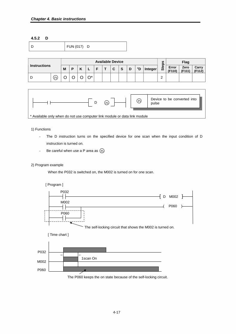
Chapter 4. Basic instructions
4-17
4.5.2 D
D FUN (017) D
Available Device FlagInstructions
M P K L F T C S D #D Integer Ste
ps
Error(F110)
Zero(F111)
Carry(F112)
D O O O O* 2
* Available only when do not use computer link module or data link module
1) Functions
� The D instruction turns on the specified device for one scan when the input condition of D
instruction is turned on.
� Be careful when use a P area as .
2) Program example
When the P032 is switched on, the M002 is turned on for one scan.
D
D
DDevice to be converted intopulseD
P032 [ D M002 ]
( P060 )
P060
M002
The self-locking circuit that shows the M002 is turned on.
P032→ ←
1scan OnM002
P060
The P060 keeps the on state because of the self-locking circuit.
[ Program ]
[ Time chart ]
D

Chapter 4. Basic instructions
4-18
The on / off toggle control (Example of D instructions)
1. Operation
When the push-button PB0 is pushed, the P060 is switched on. It is switched off when the PB0 is pushed
again. The P060 will repeat on / off whenever the PB0 is pushed.
2. System structure
3. Program
4. Time chart
0
1
2
3
.
.
.
.
Program 0
1
2
.
.
.
.
.
PB0
Digital inputmodule P00
Digital outputmodule P06
Repeat On/Off
P000 [ D M000 ]
( P060 )P060 M000
P060 M000
0000
0003
0009
[ END ]
P000
P060
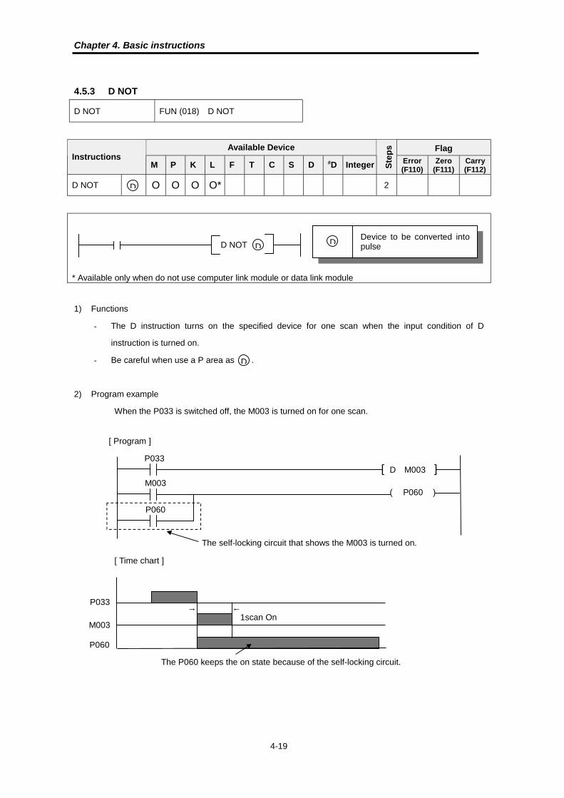
Chapter 4. Basic instructions
4-19
4.5.3 D NOT
D NOT FUN (018) D NOT
Available Device FlagInstructions
M P K L F T C S D #D Integer Ste
ps
Error(F110)
Zero(F111)
Carry(F112)
D NOT O O O O* 2
* Available only when do not use computer link module or data link module
1) Functions
� The D instruction turns on the specified device for one scan when the input condition of D
instruction is turned on.
� Be careful when use a P area as .
2) Program example
When the P033 is switched off, the M003 is turned on for one scan.
D NOT
D
DDevice to be converted intopulseD
P033 [ D M003 ]
( P060 )
P060
M003
The self-locking circuit that shows the M003 is turned on.
P033→ ←
1scan OnM003
P060
The P060 keeps the on state because of the self-locking circuit.
[ Program ]
[ Time chart ]
D

Chapter 4. Basic instructions
4-20
4.5.4 SET
SET
Available Device FlagInstructions
M P K L F T C S D #D Integer Ste
ps
Error(F110)
Zero(F111)
Carry(F112)
SET O O O O* O 1
* Available only when do not use computer link module or data link module
1) Functions
� When the input condition of SET instruction turns on, the specified device is switched on.
� The turned-on device remains on even if the input condition of SET instruction is turned off. The
device can be switched off by the RST instruction.
2) Program example
When the input condition P020 turns on, the P060 and P061 is turned on by OUT and SET
instruction.
D
D
SET D
( P060 )P020
P020 [ SET P061 ]
[ Program ]
P020
P060
P061
[ Time chart ]

Chapter 4. Basic instructions
4-21
4.5.5 RST
RST
Available Device FlagInstructions
M P K L F T C S D #D Integer Ste
ps
Error(F110)
Zero(F111)
Carry(F112)
RST O O O O* O 1
* Available only when do not use computer link module or data link module
1) Functions
� When the input condition of RST instruction turns on, the specified device is changed as described
Device Status
M, P, K, L The specified bit is turned off.
T The timer output is turned off and current value is cleared as 0
2) Program example
Set the P061 with the P020 and reset the P061 with the P021.
D
RST D
( P060 )P020
P020 [ SET P061 ]
[ RST P061 ]P021
P020
P021
P060
P061
↔
[ Program ]
[ Time chart ]

Chapter 4. Basic instructions
4-22
The countermeasure of power failure
(The difference of P area and K area)
1. The difference of I/O relay (P) and keep relay (K) with the OUT instruction
The following program shows the difference of P area and K area. Both of P060 and K000 have self-
locking circuit, and the operation of two contact is same. However, when the power is switched off and
turned on again (power failure), operations of P and K are different as shown below.
2. The difference of I/O relay (P) and keep relay (K) with the SET/RST instruction
The SET instruction makes turn a specified device on and keep the on status until the RST instruction is
executed. However, the P and K area operate differently when a power failure occurred.
( P060 )P060
PB0 PB1
( K000 )K000
PB0 PB1
PB0
PB1
P060
K000
Powerfailure ↓ ↓
Self-locking Non-volatileduring power off
Powerrecovery
PB0
[ SET P060 ]
[ SET K000 ]PB1
[ RST P060 ]
[ RST K000 ]
PB0
PB1
P060
K000
↓ ↓
Powerfailure
Powerrecovery

Chapter 4. Basic instructions
4-23
4.6 Step controller instructions
4.6.1 SET Sxx.xx
SET S
Available Device FlagInstructions
M P K L F T C S D #D Integer Ste
ps
Error(F110)
Zero(F111)
Carry(F112)
SET S O 2
* K10S1 : 0 ~ 15 K10S / K30S / K60S : 0 ~ 31 K200S / K300S / K1000S : 0 ~ 99
1) Functions
� The Sxx.xx contact will turn on when the previous step of same group and the input condition is on.
� Once a Sxx.xx is switched on, it keeps on state until the next step turns on or the step controller
group is initialized. (The Sxx.00 is switched on)
� Even if multiple input condition turn on, only one step controller is switched on.
� The Sxx.00 is initialization step and the Sxx.xx group will be initialized by switching on the Sxx.00.
When the CPU is turned to RUN mode, the Sxx.00 is set by default.
2) Program example
A sequential control by using S01.xx group
D
SET S xx.xx S xx.xx
Step No. (00 ~ 99)
Group (00 ~ 99*)
SET S01.01P030
0000
SET S01.02P031
0003
SET S01.03P032
0006
SET S01.04P033
0009
SET S01.00Reset 0012P034
S01.xx reset input condition
P030
P031
P032
P033
S01.01
S01.02
S01.03
S01.04
P034
[ Program ]
[ Time chart ]
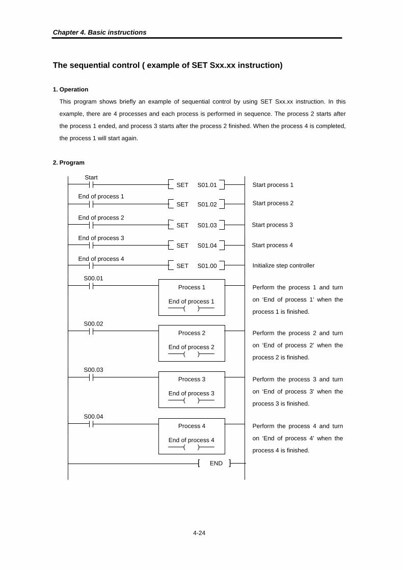
Chapter 4. Basic instructions
4-24
The sequential control ( example of SET Sxx.xx instruction)
1. Operation
This program shows briefly an example of sequential control by using SET Sxx.xx instruction. In this
example, there are 4 processes and each process is performed in sequence. The process 2 starts after
the process 1 ended, and process 3 starts after the process 2 finished. When the process 4 is completed,
the process 1 will start again.
2. Program
SET S01.01Start
SET S01.02End of process 1
SET S01.03
SET S01.04
SET S01.00
Process 1
( )End of process 1
S00.01
S00.02
S00.03
S00.04
[ END ]
Start process 1
Start process 2
Start process 3
Start process 4
Initialize step controller
End of process 2
End of process 3
End of process 4
Perform the process 1 and turn
on ‘End of process 1’ when the
process 1 is finished.
Process 2
( )End of process 2
Perform the process 2 and turn
on ‘End of process 2’ when the
process 2 is finished.
Process 3
( )End of process 3
Perform the process 3 and turn
on ‘End of process 3’ when the
process 3 is finished.
Process 4
( )End of process 4
Perform the process 4 and turn
on ‘End of process 4’ when the
process 4 is finished.

Chapter 4. Basic instructions
4-25
4.6.2 OUT Sxx.xx
OUT S
Available Device FlagInstructions
M P K L F T C S D #D Integer Ste
ps
Error(F110)
Zero(F111)
Carry(F112)
OUT S O 2
* K10S1 : 0 ~ 15 K10S / K30S / K60S : 0 ~ 31 K200S / K300S / K1000S : 0 ~ 99
1) Function
� Last-in priority control
� When the input condition turns on, the specified step controller is switched on and keep the on
status until other step controller of same group turns on.
� Only one step controller turns on even if multiple input conditions turn on. At this time, the last
turned on step controller has the highest priority.
� The Sxx.00 is initialization step and the Sxx.xx group will be initialized by switching on the Sxx.00.
When the CPU is turned to RUN mode, the Sxx.00 is set by default.
2) Program example
D
S xx.xx
Step No. (00 ~ 99)
Group (00 ~ 99*)
( Sxx.xx )
S02.xx reset input condition
P020
P021
P022
P023
S02.01
S02.23
S02.98
S02.04
P024
( S02.01 )P020
( S02.23 )P021
( S02.98 )P022
( S02.04 )P023
( S02.00 )P024
Reset
[ Program ]
[ Time chart ]
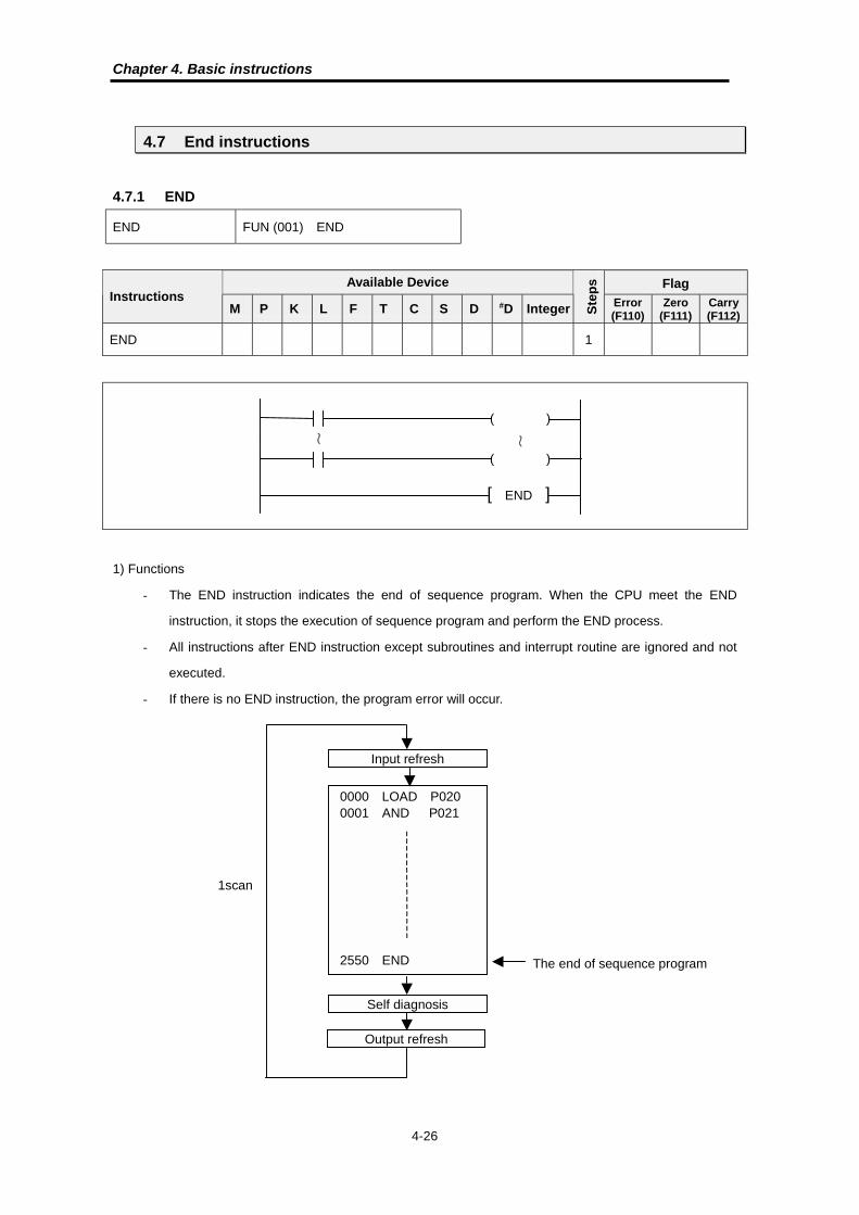
Chapter 4. Basic instructions
4-26
4.7 End instructions
4.7.1 END
END FUN (001) END
Available Device FlagInstructions
M P K L F T C S D #D Integer Ste
ps
Error(F110)
Zero(F111)
Carry(F112)
END 1
1) Functions
� The END instruction indicates the end of sequence program. When the CPU meet the END
instruction, it stops the execution of sequence program and perform the END process.
� All instructions after END instruction except subroutines and interrupt routine are ignored and not
executed.
� If there is no END instruction, the program error will occur.
( )
( )
[ END ]
Input refresh
0000 LOAD P0200001 AND P021
2550 END
Self diagnosis
Output refresh
The end of sequence program
1scan
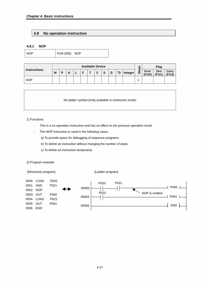
Chapter 4. Basic instructions
4-27
4.8 No operation instruction
4.8.1 NOP
NOP FUN (000) NOP
Available Device FlagInstructions
M P K L F T C S D #D Integer Ste
ps
Error(F110)
Zero(F111)
Carry(F112)
NOP 1
No ladder symbol (Only available in mnemonic mode)
1) Functions
� This is a no operation instruction and has no effect on the previous operation result.
� The NOP instruction is used in the following cases ;
a) To provide space for debugging of sequence programs.
b) To delete an instruction without changing the number of steps.
c) To delete an instruction temporarily.
2) Program example
00000
[Mnemonic program]
0000 LOAD P020
0001 AND P021
0002 NOP
0003 OUT P060
0004 LOAD P022
0005 OUT P061
0006 END
( P060 )P020
P022
[ END ]
00004
00006
( P061 )
P021
NOP is omitted
[Ladder program]

Chapter 4. Basic instructions
4-28
4.9 Timer instructions
4.9.1 TON
TON On-delay timer
Available Device FlagInstructions
M P K L F T C S D #D Integer Ste
ps
Error(F110)
Zero(F111)
Carry(F112)
Txxx OTON
O O3
1) Functions
� A timer consists of timer contact, current value, and setting value.
� The current value will start to increase when the input condition turns on. It will increase by 1 at
every 0.1 or 0.01 sec until it reaches to the setting value or input condition turns off.
� The timer contact will be switched on when the current value reaches to the setting value.
� The timer contact and current value is cleared when the input condition turns off or RST instruction
is executed.
2) Program example
The T097 (0.01 sec timer) will turn on 20 seconds later until the P020 is switched on.
V
TON
Input condition Timer setting value
Timer contact number
✼ Setting time ( t ) = Unit period (0.1 or 0.01 sec) x Setting value
Txxx V
← →t = 20sec
( Increase )
P020
T097
( P065 )
P020
T097[ TON T097 00200 ]
[ RST T097 ]P021
[Time chart]
[Program]

Chapter 4. Basic instructions
4-29
A flickering lamp (example of TON instruction)
1. Operation
By using two timers, a lamp flickers periodically while the P020 is on.
2. System diagram
3. Program
0
1
2
3
.
.
.
.
.
F
Program
0
1
2
3
. . . . .
F
StartP020
Input moduleP02
Output moduleP06
L
P020 T001 [ TON T000 00005 ]
T000 [ TON T001 00006 ]
( P065 )
[ END ]
Set a Off time (0.5sec)
Set a On time (0.6 sec)
✼ T000, T001is setas 100 msec timer
[Ladder program]
[Time chart]
T0 T1
P020
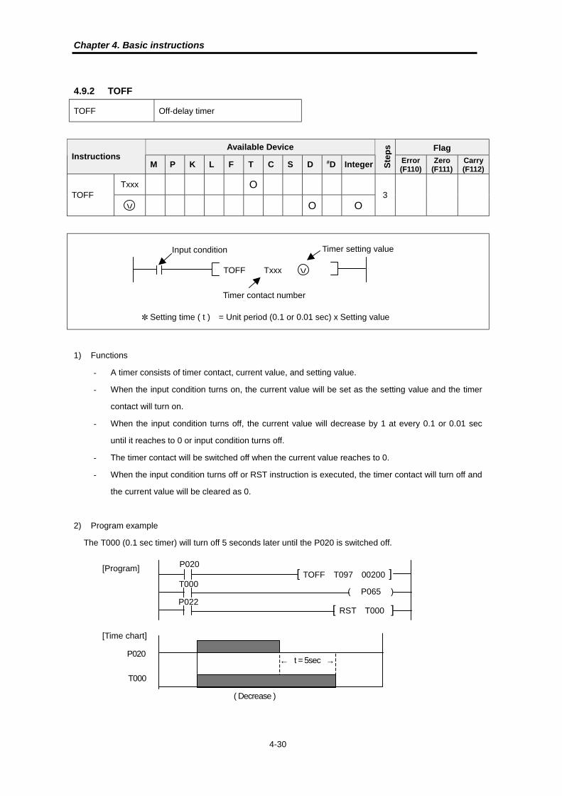
Chapter 4. Basic instructions
4-30
4.9.2 TOFF
TOFF Off-delay timer
Available Device FlagInstructions
M P K L F T C S D #D Integer Ste
ps
Error(F110)
Zero(F111)
Carry(F112)
Txxx OTOFF
O O3
1) Functions
� A timer consists of timer contact, current value, and setting value.
� When the input condition turns on, the current value will be set as the setting value and the timer
contact will turn on.
� When the input condition turns off, the current value will decrease by 1 at every 0.1 or 0.01 sec
until it reaches to 0 or input condition turns off.
� The timer contact will be switched off when the current value reaches to 0.
� When the input condition turns off or RST instruction is executed, the timer contact will turn off and
the current value will be cleared as 0.
2) Program example
The T000 (0.1 sec timer) will turn off 5 seconds later until the P020 is switched off.
V
TOFF
Input condition Timer setting value
Timer contact number
✼ Setting time ( t ) = Unit period (0.1 or 0.01 sec) x Setting value
Txxx V
← →t = 5sec
( Decrease )
P020
T000
( P065 )
P020
T000[ TOFF T097 00200 ]
[ RST T000 ]P022
[Time chart]
[Program]

Chapter 4. Basic instructions
4-31
A conveyer control (example of TOFF instruction)
1. Operation
Operate three conveyers (A, B, C) in sequence by using TOFF timers.
(Start : A – B – C, Stop : C – B – A)
2. System diagram
3. Program
0123.....
F
Pro
gra
m
Output moduleP02
Input moduleP06
Motor 2
0123.....
F
→
On/OffMC0
MC1
MC2
Motor 1 Motor 0
A
B
C
Conveyer
M2 M1 M0
( P060 )
P020
T010[ TOFF T010 00100 ]
P020[ TON T000 00050 ]
( P062 )T011
[ TOFF T011 00050 ]T000
T011
P020[ TON T001 00100 ]
( P062 )T001 P020
[ END ]
0000
0004
0006
0010
0014
0017
0021
0024
Set the off delay time of conveyer A(10sec)
Set the on delay time of conveyer B(5sec)
Set the off delay time of conveyer B(5sec)
Set the on delay time of conveyer C(5sec)
T000
T001
T10
T11
On/Off (P020)
A (P060)
B(P061)
C(P062) T011
T010
[Time chart]
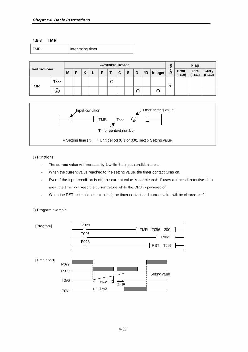
Chapter 4. Basic instructions
4-32
4.9.3 TMR
TMR Integrating timer
Available Device FlagInstructions
M P K L F T C S D #D Integer Ste
ps
Error(F110)
Zero(F111)
Carry(F112)
Txxx OTMR
O O3
1) Functions
� The current value will increase by 1 while the input condition is on.
� When the current value reached to the setting value, the timer contact turns on.
� Even if the input condition is off, the current value is not cleared. If uses a timer of retentive data
area, the timer will keep the current value while the CPU is powered off.
� When the RST instruction is executed, the timer contact and current value will be cleared as 0.
2) Program example
V
TMR
Input condition Timer setting value
Timer contact number
✼ Setting time ( t ) = Unit period (0.1 or 0.01 sec) x Setting value
Txxx V
( P061 )
P020
T096[ TMR T096 300 ]
[ RST T096 ]P023
P023
t 1= 20 t 2= 10
Setting valueP020
T096
P061 t = t1+t2
[Time chart]
[Program]

Chapter 4. Basic instructions
4-33
An alarm of drill replacement (example of TMR instruction)
1. Operation
The total usage time of the drill of a machining center is counted by PLC. If the total usage time exceeds
the lifetime of drill (100 hours), the PLC outputs an alarm signal to notice that a replacement of drill is
required.
2. System diagram
I/O Description
P020 Detect of drill down
P021 Replacement completion
P060 Turn on an alarm lamp
T000 Timer for the lifetime of drill
3. Program
0
1
2 ......
F
Program0
1
2 . . . . . .
F
Motor
Input moduleP02
Output moduleP06
L
Completionof replacement
Sensor
Drill
Alarmlamp
( P060 )
P020
C000
[ TMR T000 36000 ]
U CTU C000
R < s > 00100
[ RST T096 ]T000
C000
P021
P060
T000 1 hour timer
Counter
(1hour�100 = 100hours)

Chapter 4. Basic instructions
4-34
4.9.4 TMON
TMON Monostable timer
Available Device FlagInstructions
M P K L F T C S D #D Integer Ste
ps
Error(F110)
Zero(F111)
Carry(F112)
Txxx OTMON
O O3
1) Functions
� When the input condition turns on, the current value will be set as the setting value and starts to
decrease. The timer contact turns on when the input condition turns on.
� When the input condition turns off, the current value will decrease by 1 at every 0.1 or 0.01 sec
until it reaches to 0 and the timer contact will be switched off when the current value reaches to 0.
� While a timer is operating, on/off changed of input condition is ignored.
� When the RST instruction is executed, the timer contact will turn off and the current value will be
cleared as 0.
2) program example
V
TMON
Input condition Timer setting value
Timer contact number
✼ Setting time ( t ) = Unit period (0.1 or 0.01 sec) x Setting value
Txxx V
( P061 )
P020
T000[ TMON T000 00100 ]
[ RST T000 ]P023
P023
P020
T000
P061
← → Setting time ( t )
Setting value
[Time chart]
[Program]
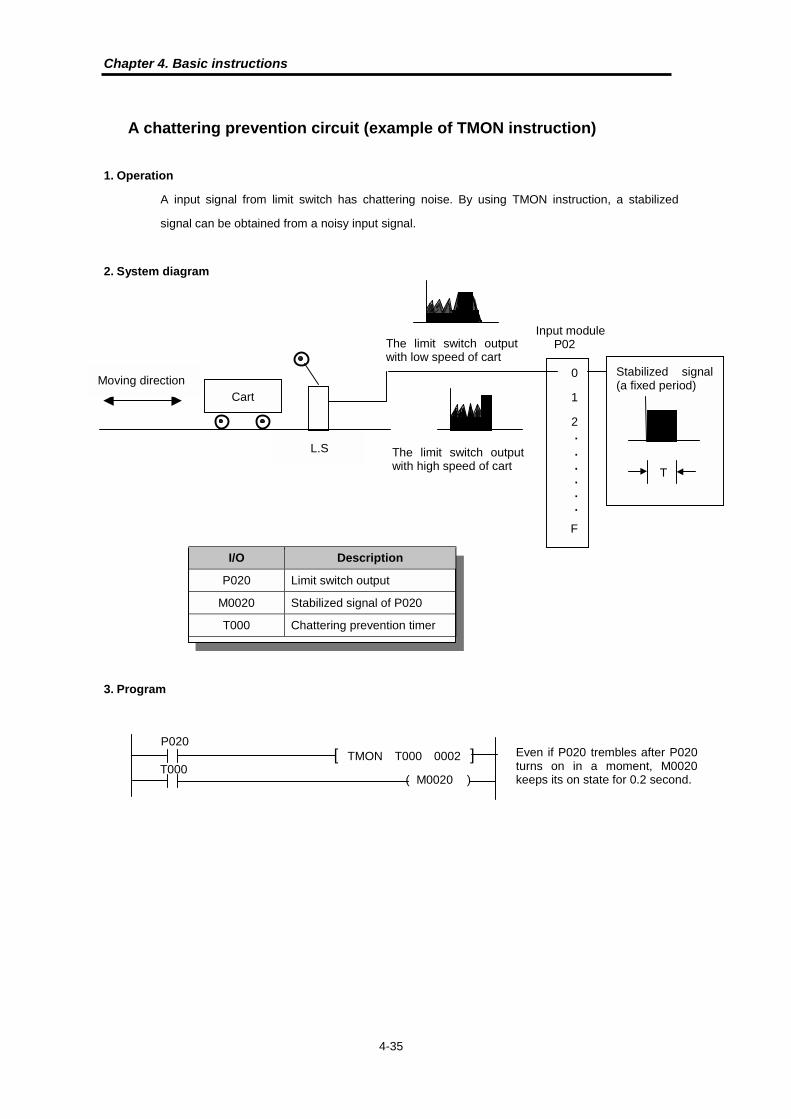
Chapter 4. Basic instructions
4-35
A chattering prevention circuit (example of TMON instruction)
1. Operation
A input signal from limit switch has chattering noise. By using TMON instruction, a stabilized
signal can be obtained from a noisy input signal.
2. System diagram
I/O Description
P020 Limit switch output
M0020 Stabilized signal of P020
T000 Chattering prevention timer
3. Program
0
1
2 ......
F
Stabilized signal(a fixed period)
T
CartMoving direction
L.S
The limit switch outputwith low speed of cart
The limit switch outputwith high speed of cart
Input module P02
( M0020 )
P020
T000 [ TMON T000 0002 ] Even if P020 trembles after P020
turns on in a moment, M0020keeps its on state for 0.2 second.
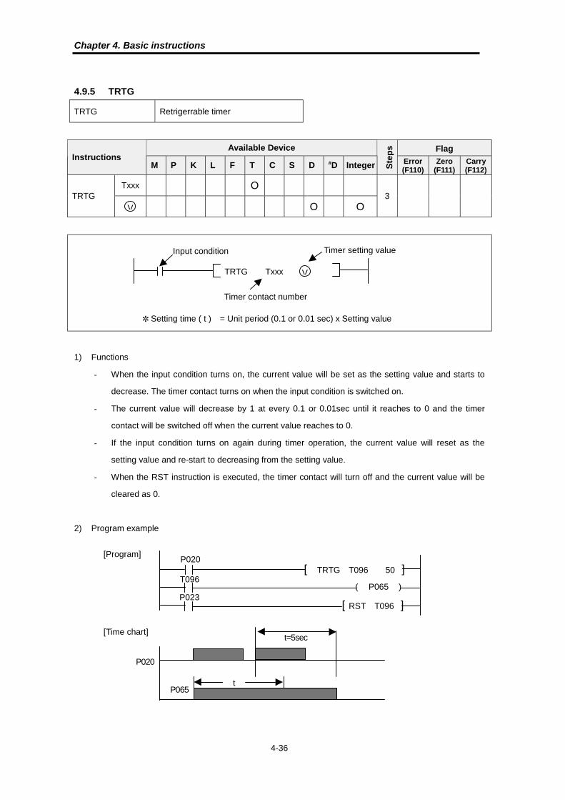
Chapter 4. Basic instructions
4-36
4.9.5 TRTG
TRTG Retrigerrable timer
Available Device FlagInstructions
M P K L F T C S D #D Integer Ste
ps
Error(F110)
Zero(F111)
Carry(F112)
Txxx OTRTG
O O3
1) Functions
� When the input condition turns on, the current value will be set as the setting value and starts to
decrease. The timer contact turns on when the input condition is switched on.
� The current value will decrease by 1 at every 0.1 or 0.01sec until it reaches to 0 and the timer
contact will be switched off when the current value reaches to 0.
� If the input condition turns on again during timer operation, the current value will reset as the
setting value and re-start to decreasing from the setting value.
� When the RST instruction is executed, the timer contact will turn off and the current value will be
cleared as 0.
2) Program example
V
TRTG
Input condition Timer setting value
Timer contact number
✼ Setting time ( t ) = Unit period (0.1 or 0.01 sec) x Setting value
Txxx V
( P065 )
P020
T096[ TRTG T096 50 ]
[ RST T096 ]P023
P065t
P020
t=5sec[Time chart]
[Program]

Chapter 4. Basic instructions
4-37
The fault of conveyer detecting circuit (example of TRTG instruction)
1. Operation
Detect the fault of conveyer by check that a product is passed within a specified period or not.
2. System diagram
3. Program
0
1
2 ......
F
Input moduleP02
Conveyer
Detector
Supplier
( M100 )
P020
T005 [ TRTG T005 00200 ] If there is no product passing during 20
seconds, the timer turns off and M100 isswitched off.During normal operation, the M100keeps on state.
Detectingsignal
P020
T=20sec
T5
M100
Timercontact
Operatingindicator
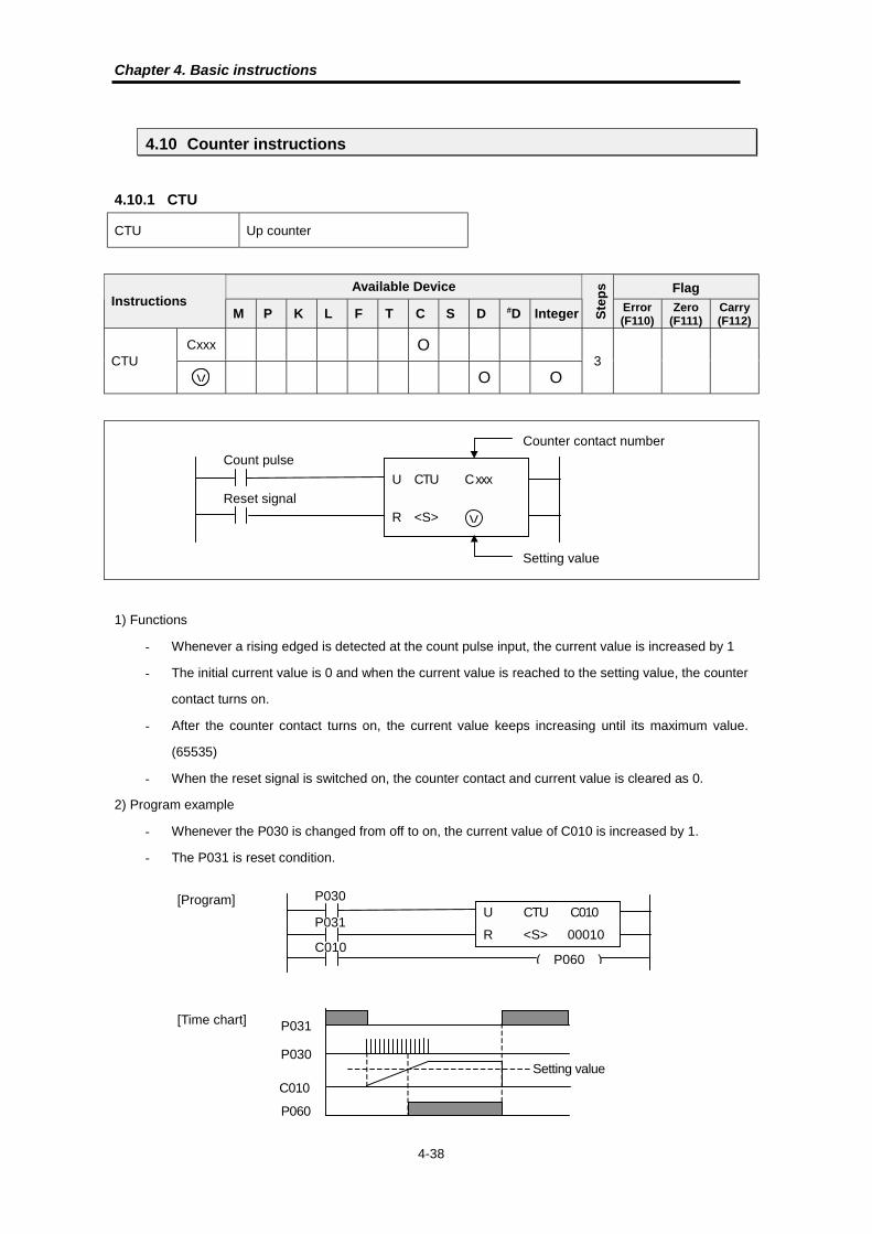
Chapter 4. Basic instructions
4-38
4.10 Counter instructions
4.10.1 CTU
CTU Up counter
Available Device FlagInstructions
M P K L F T C S D #D Integer Ste
ps
Error(F110)
Zero(F111)
Carry(F112)
Cxxx OCTU
O O3
1) Functions
� Whenever a rising edged is detected at the count pulse input, the current value is increased by 1
� The initial current value is 0 and when the current value is reached to the setting value, the counter
contact turns on.
� After the counter contact turns on, the current value keeps increasing until its maximum value.
(65535)
� When the reset signal is switched on, the counter contact and current value is cleared as 0.
2) Program example
� Whenever the P030 is changed from off to on, the current value of C010 is increased by 1.
� The P031 is reset condition.
V
P030
P031U CTU C010
R <S> 00010
( P060 )C010
Setting value
P031
C010
P060
P030
[Time chart]
[Program]
V
Count pulse
Reset signal
U CTU
R <S>
Counter contact number
Setting value
C xxx
V

Chapter 4. Basic instructions
4-39
4.10.2 CTD
CTD Down counter
Available Device FlagInstructions
M P K L F T C S D #D Integer Ste
ps
Error(F110)
Zero(F111)
Carry(F112)
Cxxx OCTD
O O3
1) Functions
� Whenever the rising edge is detected from counter pulse input, the current value is decreased by 1.
� The initial current value is the setting value, and when the current value reached to 0, the counter
contact is switched on.
� When the reset signal turns on, the counter contact is switched off and the current value is reset as
the setting value.
2) Program example
� Whenever the P030 is changed from off to on, the current value of C010 is decreased by 1.
� The P031 is reset condition.
V
P030
P031D CTD C010
R <S> 00010
( P060 )C010
Setting value
P031
P030
C010
P060
[Time chart]
[Program]
Count pulse
Reset signal
U CTD
R <S>
Counter contact number
Setting value
V
C xxx

Chapter 4. Basic instructions
4-40
4.10.3 CTUD
CTUD Up-down counter
Available Device FlagInstructions
M P K L F T C S D #D Integer Ste
ps
Error(F110)
Zero(F111)
Carry(F112)
Cxxx OCTUD
O O3
1) Functions
� Whenever a rising edged is detected from up count input, the current value is increased by 1.
� The current value is decreased by 1 whenever a rising edge is detected at the down count input.
� The initial current value is 0.
� The counter contact turns on when the current value is same or greater than the setting value.
� When the reset signal turns on, the counter contact and current value is cleared as 0.
2) Program example
� The P030 is up count input, and the P031 is down count input.
� The P032 is reset signal.
V
P030
P031U CTUD C000
R <S> 00010
( P060 )C000
P032D
P030
Setting value
P032
C000
P031
[Time chart]
[Program]
Counter contact number
U CTUD
R <S>
D
Setting value
Up count
Down count
Reset signal
C xxx
V
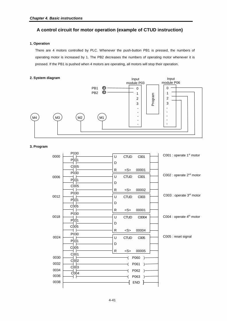
Chapter 4. Basic instructions
4-41
A control circuit for motor operation (example of CTUD instruction)
1. Operation
There are 4 motors controlled by PLC. Whenever the push-button PB1 is pressed, the numbers of
operating motor is increased by 1. The PB2 decreases the numbers of operating motor whenever it is
pressed. If the PB1 is pushed when 4 motors are operating, all motors will stop their operation.
2. System diagram
3. Program
0
1
2
3.....
Pro
gra
m
Inputmodule P03
Inputmodule P06
0
1
2
3.....
M3 M2 M1
PB1 PB2
M4
0006
( P060 )
P030
P031U CTUD C001
R <S> 00001C005
D
P030
P031U CTUD C001
R <S> 00002C005
D
P030
P031U CTUD C003
R <S> 00001C005
D
P030
P031U CTUD C0004
R <S> 00004C005
D
P030
P031U CTUD C005
R <S> 00005C005
D
C001
( P061 )C002
( P062 )C003
( P063 )C004
[ END ]
0000
0012
0018
0024
0030
0032
0036
0034
0038
C001 : operate 1st motor
C002 : operate 2nd motor
C003 : operate 3rd motor
C004 : operate 4th motor
C005 : reset signal
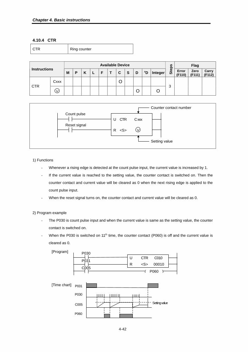
Chapter 4. Basic instructions
4-42
4.10.4 CTR
CTR Ring counter
Available Device FlagInstructions
M P K L F T C S D #D Integer Ste
ps
Error(F110)
Zero(F111)
Carry(F112)
Cxxx OCTR
O O3
1) Functions
� Whenever a rising edge is detected at the count pulse input, the current value is increased by 1.
� If the current value is reached to the setting value, the counter contact is switched on. Then the
counter contact and current value will be cleared as 0 when the next rising edge is applied to the
count pulse input.
� When the reset signal turns on, the counter contact and current value will be cleared as 0.
2) Program example
� The P030 is count pulse input and when the current value is same as the setting value, the counter
contact is switched on.
� When the P030 is switched on 11th time, the counter contact (P060) is off and the current value is
cleared as 0.
V
Counter contact number
Count pulse
Reset signal
U CTR
R <S>
Setting value
C xxx
V
P030
P031U CTR C010
R <S> 00010
( P060 )C005
P031
C005
P060
P030
Setting value
[Time chart]
[Program]
Chapter 5 Application instructions
5.1 Data transfer instructions.................................................... 5-1
5.1.1 MOV, MOVP, DMOV, DMOVP .................................................. 5-1
5.1.2 CMOV, CMOVP, DCMOV, DCMOVP........................................ 5-3
5.1.3 GMOV, GMOVP........................................................................ 5-5
5.1.4 FMOV, FMOVP......................................................................... 5-7
5.1.5 BMOV, BMOVP ........................................................................ 5-9
5.2 Conversion instructions .....................................................5-11
5.2.1 BCD, BCDP, DBCD, DBCDP...................................................5-11
5.2.2 BIN, BINP, DBIN, DBINP ........................................................ 5-14
5.3 Comparison instructions ....................................................5-16
5.3.1 CMP, CMPP, DCMP, DCMPP ................................................. 5-16
5.3.2 TCMP, TCMPP, DTCMP, DTCMPP......................................... 5-19
LD ( =, >, <, >=, <=, <> )....................................................................... 5-21
5.3.4 AND ( =, >, <, >=, <=, <>)....................................................... 5-22
5.3.5 OR ( =, >, <, >=, <=, <>) ......................................................... 5-23
5.4 Increment/decrement operations .......................................5-24
5.4.1 INC, INCP, DINC, DINCP ....................................................... 5-24
5.4.2 DEC, DECP, DDEC, DDECP.................................................. 5-26
5.5 Rotation instructions ..........................................................5-28
5.5.1 ROL, ROLP, DROL, DROLP................................................... 5-28
5.5.2 ROR, RORP, DROR, DRORP ................................................ 5-30
5.5.3 RCL, RCLP, DRCL, DRCLP ................................................... 5-32
5.5.4 RCR, RCRP, DRCR, DRCRP ................................................. 5-34
5.6 Shift instructions ................................................................5-36
5.6.1 BSFT, BSFTP ......................................................................... 5-36
5.6.2 WSFT, WSFTP ....................................................................... 5-38
5.6.3 SR .......................................................................................... 5-40
5.7 Exchange instructions .......................................................5-42

5.7.1 XCHG, XCHGP, DXCHG, DXCHGP....................................... 5-42
5.8 BIN arithmetic instructions .................................................5-44
5.8.1 ADD, ADDP, DADD, DADDP.................................................. 5-44
5.8.2 SUB, SUBP, DSUB, DSUBP................................................... 5-46
5.8.3 MUL, MULP, DMUL, DMULP.................................................. 5-48
5.8.4 MUL, MULP, DMUL, DMULP.................................................. 5-50
5.8.5 DIV, DIVP, DDIV, DDIVP......................................................... 5-52
5.8.6 DIVS, DIVSP, DDIVS, DDIVSP............................................... 5-54
5.9 BCD arithmetic instructions ...............................................5-56
5.9.1 ADDB, ADDBP, DADDB, DADDBP ........................................ 5-56
5.9.2 SUBB, SUBBP, DSUBB, DSUBBP ......................................... 5-58
5.9.3 MULB, MULBP, DMULB, DMULBP ........................................ 5-60
5.9.4 DIVB, DIVBP, DDIVB, DDIVBP............................................... 5-62
5.10 Logical arithmetic instructions .......................................5-64
5.10.1 WAND, WANDP, DWAND, DWANDP..................................... 5-64
5.10.2 WOR, WORP, DWOR, DWORP ............................................. 5-66
5.10.3 WXOR, WXORP, DWXOR, DWXORP.................................... 5-68
5.10.4 WXNR, WXNRP, DWXNR, DWXNRP .................................... 5-70
5.11Data processing instructions..............................................5-72
5.11.1 SEG, SEGP............................................................................ 5-72
5.11.2 ASC, ASCP ............................................................................ 5-75
5.11.3 BSUM, BSUMP, DBSUM, DBSUMP....................................... 5-77
5.11.4 ENCO, ENCOP ...................................................................... 5-79
5.11.5 DECO, DECOP ...................................................................... 5-81
5.11.6 FILR, FILRP, DFILR, DFILRP................................................. 5-83
5.11.7 FILW, FILWP, DFILW, DFILWP ............................................... 5-85
5.11.8 DIS, DISP ............................................................................... 5-87
5.11.9 UNI, UNIP............................................................................... 5-89
5.11.10 IORF, IORFP .......................................................................... 5-91
5.12 System instructions.......................................................5-93
5.12.1 FALS....................................................................................... 5-93
5.12.2 DUTY...................................................................................... 5-94
5.12.3 WDT, WDTP ........................................................................... 5-96
5.12.4 OUTOFF................................................................................. 5-98
5.12.5 STOP...................................................................................... 5-99
5.13 Branch instructions .....................................................5-100
5.13.1 JMP, JME.............................................................................. 5-100
5.13.2 CALL, CALLP, SBRT, RET ................................................... 5-102

5.14 Loop instructions.........................................................5-104
5.14.1 FOR, NEXT .......................................................................... 5-104
5.14.2 BREAK ................................................................................. 5-105
5.15 Flag instructions..........................................................5-106
5.15.1 STC, CLC ............................................................................. 5-106
5.15.2 CLE ...................................................................................... 5-107
5.16 Special module instructions ........................................5-108
5.16.1 GET, GETP........................................................................... 5-108
5.16.2 PUT, PUTP ............................................................................5-110
5.17 Data link instructions...................................................5-112
5.17.1 READ.....................................................................................5-112
5.17.2 WRITE...................................................................................5-115
5.17.3 RGET.....................................................................................5-117
5.17.4 RPUT.................................................................................... 5-120
5.17.5 STATUS................................................................................ 5-122
5.18 Inturrupt instructions ...................................................5-123
5.18.1 EI, DI .................................................................................... 5-123
5.18.2 TDINT, IRET ......................................................................... 5-124
5.18.3 INT, IRET.............................................................................. 5-125
5.19 Sign inversion instruction ............................................5-126
5.19.1 NEG, NEGP, DNEG, DNEGP ............................................... 5-126
5.20 Bit contact instructions ................................................5-128
5.20.1 BLD, BLDN........................................................................... 5-128
5.20.2 BAND, BANDN ..................................................................... 5-129
5.20.3 BAND, BANDN ..................................................................... 5-130
5.20.4 BOUT.................................................................................... 5-131
5.20.5 BSET, BRST ......................................................................... 5-132
5.21 Computer link module instructions ..............................5-133
5.21.1 SND...................................................................................... 5-133
5.21.2 RCV...................................................................................... 5-134
5.22 High speed counter instructions ..................................5-135
5.22.1 HSCNT ................................................................................. 5-135
5.22.2 HSC...................................................................................... 5-137
5.23 RS-485 communication instructions............................5-139
5.23.1 RECV.................................................................................... 5-139
5.23.2 SEND.................................................................................... 5-141


Chapter 5. Application instructions
5-1
5 Application Instructions
5.1 Data transfer instructions
5.1.1 MOV, MOVP, DMOV, DMOVP
MOV
(Move)
FUN(80) MOV FUN(82) DMOV
FUN(81) MOVP FUN(83) DMOCP
Applicable
CPUAll CPUs
Available Device FlagInstructions
M P K L F T C S D #D IntegerSteps Error
(F110)Zero
(F111)Carry(F112)
O O O O* O O O O O OMOV(P)
DMOV(P) O O O O* O O O O5/7 O
* Available only when do not use computer link module or data link module
1) Functions
� MOV(P) : Transfer the 16-bits data of the device specified at [ S ] to the device specified at [ D ].
� DMOV(P) : Transfer the 32-bits data of the device specified at [ S+1, S ] to the device specified at
[ D+1, D ].
Operand setting
D
S
MOV
MOVP
DMOV
DMOVP
S D
S D
The source device at whichthe data to be transferred isstored.
The device of transferdestinationD
S
16 bits
D
S 0 1 1 1 0 0 0 0 1 1 1 1 0 0 1 1
0 1 1 1 0 0 0 0 1 1 1 1 0 0 1 1
0 1 1 0 1
0 1 1 0 1
16 bits
1 0
1 0
+ 1D
S + 1
16 bits
1 0 0 1 1 0 1
1 0 0 1 1 0 1
D
S

Chapter 5. Application instructions
5-2
� Execution condition
2) Program example
Whenever a rising edge is detected at the P020, the ‘h00F3’ is moved to the P04 word.
MOVP h70F3 P04
P020
Input condition
MOV, DMOV
MOVP, DMOVP
Executed only once Executed only once
Executed per scan Executed per scan
0 1 1 1 0 0 0 0 1 1 1 1 0 0 1 1
P04F P040

Chapter 5. Application instructions
5-3
5.1.2 CMOV, CMOVP, DCMOV, DCMOVP
CMOV
(Complement move)
FUN(84) CMOV FUN(86) DCMOV
FUN(85) CMOVP FUN(87) DCMOCP
Applicable
CPUAll CPUs
Available Device FlagInstructions
M P K L F T C S D #D IntegerSteps Error
(F110)Zero
(F111)Carry(F112)
O O O O* O O O O O OCMOV(P)
DCMOV(P) O O O O* O O O O5/7 O
* Available only when do not use computer link module or data link module
1) Functions
� CMOV(P) : Reverses the 16-bits data of [ S ] per bit and transfers the result to [ D ].
� DCMOV(P) : Reverses the 32-bits data of [ S+1, S ] per bit and transfers the result to [ D+1, D ].
Operand setting
D
S
CMOV
CMOVP
DCMOV
DCMOVP
S D
S D
The source device at whichthe data to be transferred isstored.
The device at which thereversed result is stored
D
S
16 bits
D
S 0 1 1 1 0 0 0 0 1 1 1 1 0 0 1 1
1 0 0 0 1 1 1 1 0 0 0 0 1 1 0 0
Reverse
16 bits
0 1 1 0 0 1 0
1 0 0 1 1 0 1
D
S
16 bits
0 1 1 0 0 1 0
1 0 0 1 1 0 1
+ 1D
S + 1
Reverse Reverse

Chapter 5. Application instructions
5-4
� Execution conditions
2) Program example
� While the M020 is on, reverse the data of P02 word and transfer the result to P06 word.
CMOV P02 P06
M020
16 bits
0 0 1 1 1 0 0 0 1 1 0 1 0 0 1 1
1 1 0 0 0 1 1 1 0 0 1 0 1 1 0 0
Reverse
P02
P06
Input condition
CMOV, DCMOV
CMOVP, DCMOVP
Executed only once Executed only once
Executed per scan Executed per scan
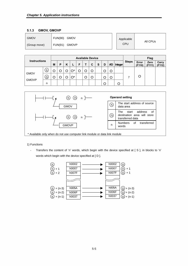
Chapter 5. Application instructions
5-5
5.1.3 GMOV, GMOVP
GMOV
(Group move)
FUN(90) GMOV
FUN(91) GMOVP
Applicable
CPUAll CPUs
Available Device FlagInstructions
M P K L F T C S D #D IntegerSteps Error
(F110)Zero
(F111)Carry(F112)
O O O O* O O O O O
O O O O* O O O OGMOV
GMOVP
O O
7 O
* Available only when do not use computer link module or data link module
1) Functions
� Transfers the content of ‘n’ words, which begin with the device specified at [ S ], in blocks to ‘n’
words which begin with the device specified at [ D ].
Operand setting
GMOV
GMOVP
S D
S D
The start address of sourcedata area
The start address ofdestination area will storetransferred data
D
D
S
S
n
n
Numbers of transferredwordsn
h0002
h0007
h007F
h005A
h006F
h0037
h0002
h0007
h007F
h005A
h006F
h0037
+ 1DS + 1
S + 2 + 1D
S + (n-3) D
S + (n-2) D
S + (n-1) D
+ (n-3)
+ (n-2)
+ (n-1)
DS
n

Chapter 5. Application instructions
5-6
� Execution conditions
2) Program example
� While the P020 is on, move the data of D000, D001, and D002 to P04, P05, and P06 area.
Input condition
GMOV
GMOVP
Executed only once Executed only once
Executed per scan Executed per scan
h0001
h0004
h005F
h0001
h0004
h005F
D0000
D0001
D0002
P04
P05
P06
DS
n
GMOV D0000 P04 3
P020

Chapter 5. Application instructions
5-7
5.1.4 FMOV, FMOVP
FMOV
(File move)
FUN(92) FMOV
FUN(93) FMOVP
Applicable
CPUAll CPUs
Available Device FlagInstructions
M P K L F T C S D #D IntegerSteps Error
(F110)Zero
(F111)Carry(F112)
O O O O* O O O O O
O O O O* O O O OFMOV
FMOVP
O O
7 O
* Available only when do not use computer link module or data link module
1) Functions
� Transfers the content of device specified at [ S ] in blocks to ‘n’ points which begin with the device
specified at [ D ].
Operand setting
FMOV
FMOVP
S D
S D
The device at which sourcedata area is stored
The start address ofdestination area will storetransferred data
D
D
S
S
n
n
Numbers of transferredwordsn
n
h005A
h005A
h005A
h005A
h005A
h005A
+ 1D+ 1D
D
D
D
+ (n-3)
+ (n-2)
+ (n-1)
D
S h005A n words

Chapter 5. Application instructions
5-8
� Execution condition
2) Program example
� Whenever a rising edge is detected at P030, transfer the content of P02 word to the block of P04,
P05, and P06.
Input condition
FMOV
FMOVP
Executed only once Executed only once
Executed per scan Executed per scan
FMOVP P02 P04 3
P020
h0098 P02 h0098
h0098
h0098
P04
P05
P06

Chapter 5. Application instructions
5-9
5.1.5 BMOV, BMOVP
BMOV
(Bit move)
FUN(100) BMOV
FUN(101) BMOVP
Applicable
CPUAll CPUs
Available Device FlagInstructions
M P K L F T C S D #D IntegerSteps Error
(F110)Zero
(F111)Carry(F112)
O O O O* O O O O O
O O O O* O O O OBMOV
BMOVP
O
7 O
* Available only when do not use computer link module or data link module
1) Functions
� The format of ‘Cw’
a) s : The start bit of [ S ].
b) d : The start bit of [ D ]
c) zz : Numbers of transferred bits. (Hexadecimal)
� Transfers the content of ‘zz’ bits from the ‘s’ bit of the device specified at [ S ] to the ‘zz’ bits from ‘d’
bit of the device specified at [ D ].
� The maximum value of the ‘zz’ is h10 ( = 16). If the value of ‘zz’ is 0 or over h10, the instruction will
be ignored. (The error flag F110 is set when the ‘zz’ is over h10.)
Operand setting
BMOV
BMOVP
S D
S D
The device at which sourcedata is stored
The device which will storetransferred dataD
D
S
S
Cw
CwInformation for start bit andnumbers of transferred bitsCw
Cw
h s d z z

Chapter 5. Application instructions
5-10
� Execution condition
2) Program example
- Whenever a rising edge is detected at the P030, transfer 4 bits from the P020 bit to the 4 bits from the
P063 bit.
Input condition
BMOV
BMOVP
Executed only once Executed only once
Executed per scan Executed per scan
BMOVP P02 P06 h0304
P030
1 0 0 1 1
P02F P020
1 0 0 1 1
P06F P060P063
P023
P066
4bits
4bits

Chapter 5. Application instructions
5-11
5.2 Conversion instructions
5.2.1 BCD, BCDP, DBCD, DBCDP
BCD
(Binary coded
decimal)
FUN(60) BCD FUN(62) DBCD
FUN(61) BCDP FUN(63) DBCDP
Applicable
CPUAll CPUs
Available Device FlagInstructions
M P K L F T C S D #D IntegerSteps Error
(F110)Zero
(F111)Carry(F112)
O O O O* O O O O OBCD(P)
DBCD(P) O O O O* O O O O5 O
* Available only when do not use computer link module or data link module
1) Functions
� BCD : Converts binary data (0 to 9999) of the device specified at [ S ] into BCD format and
transfers the result to the device specified at [ D ].
� DBCD : Converts binary data (0 to 99999999) of the device specified at [ S ] into BCD format and
transfers the result to the device specified at [ D ].
Operand setting
D
S
BCD
BCDP
DBCD
DBCDP
S D
S D
The source device at whichthe data to be converted toBCD format is stored
The device at which theconverted result is stored
D
S
1
8192
0
4096
0
32768
0
16384
1
512
1
256
0
2048
1
1024
0
32
0
16
0
128
0
64
1
2
1
1
1
8
1
4
0
2000
1
1000
1
8000
0
4000
0
200
1
100
1
800
0
400
0
20
1
10
1
80
0
40
0
2
1
1
1
8
0
4
Be sure to set as 0.(BCD conversion willbe exceeded if not)
BIN (9999)
BCD (9999)D
S
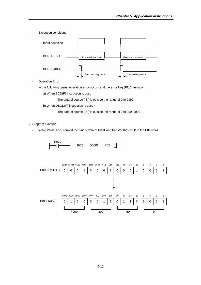
Chapter 5. Application instructions
5-12
� Execution conditions
� Operation Error
In the following cases, operation error occurs and the error flag (F110) turns on.
a) When BCD(P) instruction is used
The data of source [ S ] is outside the range of 0 to 9999
b) When DBCD(P) instruction is used
The data of source [ S ] is outside the range of 0 to 99999999
2) Program example
� While P020 is on, convert the binary data of D001 and transfer the result to the P05 word.
Input condition
BCD, DBCD
BCDP, DBCDP
Executed only once Executed only once
Executed per scan Executed per scan
BCD D0001 P05
P020
0
8192
1
4096
0
32768
0
16384
0
512
1
256
0
2048
0
1024
0
32
1
16
0
128
0
64
0
2
1
1
0
8
0
4
0
2000
0
1000
0
8000
1
4000
1
200
1
100
0
800
0
400
1
20
0
10
0
80
1
40
0
2
1
1
1
8
0
4
D0001 (h1111)
P05 (4369)
4000 300 60 9

Chapter 5. Application instructions
5-13
Displaying the current value of counter
(example of BCD, BMOV instructions)
1. Operation
There is a warehouse and numbers of product incoming / outgoing are counted by light switches. The
current stock of inside of warehouse is displayed by a digital indicator. When the stock of inside of
warehouse reaches to 30, the incoming conveyer will be stopped.
2. System diagram
3. Program
Conveyer motor
! ! ! ! !!! ! !
! ! !! ! ! !
! ! ! ! ! !
Incoming
!
!
(P030)
Light S/W
!
!
(P031)
Light S/W
Light S/W
! Outgoing
0
1
2
3
4
5
6
7
∙
F
0
1
2
3
∙
∙
∙
∙
∙
∙P
rogra
m
Input moduleP03
Output moduleP04
Outputmodule
P06
"
M
0∙∙F
1 8
Counter reset S/W (P032)
Digital indicator
F010
U CTUD C000
D
R <S> 0003
P031
P030
( P06F )
[ BCD C000 M000 ]
C000
P032
[ BMOV M000 P04 h0008 ]
[END ]
0000
0006
0008
0021
Convert the current value ofcounter to BCD format
Display only last 8bits (2 digit)
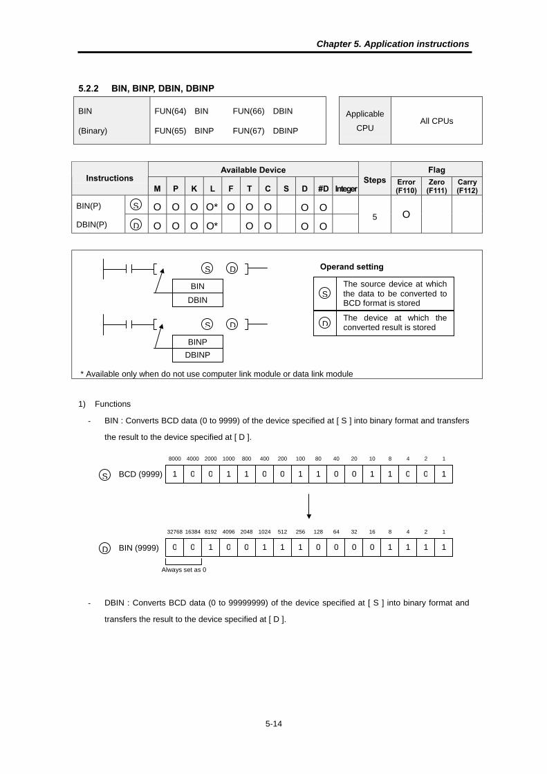
Chapter 5. Application instructions
5-14
5.2.2 BIN, BINP, DBIN, DBINP
BIN
(Binary)
FUN(64) BIN FUN(66) DBIN
FUN(65) BINP FUN(67) DBINP
Applicable
CPUAll CPUs
Available Device FlagInstructions
M P K L F T C S D #D IntegerSteps Error
(F110)Zero
(F111)Carry(F112)
O O O O* O O O O OBIN(P)
DBIN(P) O O O O* O O O O5 O
* Available only when do not use computer link module or data link module
1) Functions
� BIN : Converts BCD data (0 to 9999) of the device specified at [ S ] into binary format and transfers
the result to the device specified at [ D ].
� DBIN : Converts BCD data (0 to 99999999) of the device specified at [ S ] into binary format and
transfers the result to the device specified at [ D ].
Operand setting
D
S
BIN
BINP
DBIN
DBINP
S D
S D
The source device at whichthe data to be converted toBCD format is stored
The device at which theconverted result is storedD
S
1
8192
0
4096
0
32768
0
16384
1
512
1
256
0
2048
1
1024
0
32
0
16
0
128
0
64
1
2
1
1
1
8
1
4
0
2000
1
1000
1
8000
0
4000
0
200
1
100
1
800
0
400
0
20
1
10
1
80
0
40
0
2
1
1
1
8
0
4
Always set as 0
BCD (9999)
BIN (9999)D
S

Chapter 5. Application instructions
5-15
� Execution conditions
� Operation Error
In the following cases, operation error occurs and the error flag (F110) turns on.
a) Each digit (4 bits) of source [ S ] is outside the range of 0 to 9
(Example : [ S ] = h78A5)
2) Program example
� While P020 is on, convert the BCD data of P00 word and transfer the result to the D0001.
Input condition
BIN, DBIN
BINP, DBINP
Executed only once Executed only once
Executed per scan Executed per scan
BIN P00 D0001
P020
0
8192
1
4096
0
32768
0
16384
0
512
1
256
0
2048
0
1024
0
32
1
16
0
128
0
64
0
2
1
1
0
8
0
4
0
2000
0
1000
0
8000
1
4000
1
200
1
100
0
800
0
400
1
20
0
10
0
80
1
40
0
2
1
1
1
8
0
4
D0001 (h1111)
P00 (4369)
4000 300 60 9

Chapter 5. Application instructions
5-16
5.3 Comparison instructions
5.3.1 CMP, CMPP, DCMP, DCMPP
CMP
(Compare)
FUN(50) CMP FUN(52) DCMP
FUN(51) CMPP FUN(53) DCMPP
Applicable
CPUAll CPUs
Available Device FlagInstructions
M P K L F T C S D #D IntegerSteps Error
(F110)Zero
(F111)Carry(F112)
O O O O O O O O O OCMP(P)
DCMP(P) O O O O O O O O O O5 / 9 O
1) Functions
� Compares contents of two devices specified at [ S1 ] and [ S2 ].
� After comparing, set corresponding flag among F120 ~ F125.
F120 F121 F122 F123 F124 F125Flag
< ≤ = > ≥ ≠
> 0 0 0 1 1 1
< 1 1 0 0 0 1
= 0 1 1 0 1 0
� Above flags indicate the result of CMP instruction executed at last.
� The error flag (F110) is set when [ S1 ] or [ S2 ] specified as #D format is over device range. The
instruction at which error occurred is not executed.
Operand setting
S1
CMP
CMPP
DCMP
DCMPP
Data to be compared
S2
S1
S1
S2
S2
S1
S2
S1 S2
S1 S2
S1 S2

Chapter 5. Application instructions
5-17
� Execution conditions
2) Program example
� While P020 is on, compare contests of D000 and D001 and set flags according to the result.
F120 F121 F122 F123 F124 F125Flag
< ≤ = > ≥ ≠
Result 1 1 0 0 0 1
Input condition
CMP, DCMP
CMPP, DCMPP
Executed only once Executed only once
Executed per scan Executed per scan
0 0 0 1 0 0 0 (h0008)(D0000)
0 0 1 0 0 0 1 (h2001)(D0001)
( M0000 )
( M0001 )
( M0002 )
END
CMP D0000 D0001
F120
F123
F122
[ Program ]
[ Flag setting ]

Chapter 5. Application instructions
5-18
Comparing circuit (example of CMP instruction)
1. Operation
There is a up-down counter C000. P030 is up-count input, and P031 is down-count input. If the current
value of timer is 0 ~ 9, P060 turns on. If the current value is 10 ~ 19, P061 will be on. P062 will turn on
when 20 ~ 29, P063 will turn on when 30 ~ 39, and P064 will be on when the current value is 40 or
larger.
2. Program
U CTUD C000
D
R <S> 00050
P030
P031
P032
F010CMP C000 00010
F120( M0000 )
F010CMP C000 00020
F120( M0001 )
F010CMP C000 00030
F120( M0002 )
F010CMP C000 00040
F120( M0003 )
M0000( P060 )
M0000( P061 )
M0001
M0001( P062 )
M0002
M0002( P063 )
M0003
M0003( P064 )
END
0000
0006
0014
0012
0020
0028
0022
0030
0038
0036
0040
0046
0043
0051
0049
0 ~ 10
Less than 40
10 ~ 19
30 ~ 39
20 ~ 29
40 or more
Less than 30
Less than 20
Less than 10
C000 : the current value ofcounter

Chapter 5. Application instructions
5-19
5.3.2 TCMP, TCMPP, DTCMP, DTCMPP
TCMP
(Table compare)
FUN(54) TCMP FUN(56) DTCMP
FUN(55) TCMPP FUN(57) DTCMPP
Applicable
CPUAll CPUs
Available Device FlagInstructions
M P K L F T C S D #D IntegerSteps Error
(F110)Zero
(F111)Carry(F112)
O O O O O O O O O O
O O O O O O O O OTCMP(P)
DTCMP(P)O O O O* O O O O
7 / 9 O O
* Available only when do not use computer link module or data link module
1) Functions
� Compares content of the device specified at [ S1 ] with each contents of 16 words from the device
specified at [ S2 ].
� The comparison result (If two words are same, 1 is output. If not, 0 is output) consists of 16 bits,
and they are stored at the device specified at [ D ].
� If all comparison result are 0, then the zero flag (F111) is switched on. ( [ D ] = 0)
� Execution conditions
Operand setting
TCMP
TCMPP
DTCMP
DTCMPP
Data to be compared
The device at which thecomparison result is stored
S1
S1
S2
S2
S1
S2
D
The start address of blockto be compared with S1
S1
S2
D
D
D
Input condition
TCMP
TCMPP
Executed only once Executed only once
Executed per scan Executed per scan
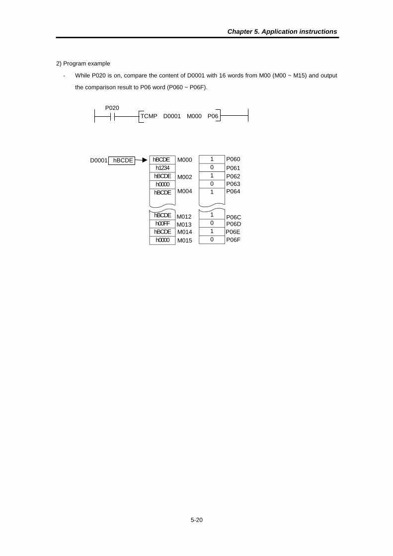
Chapter 5. Application instructions
5-20
2) Program example
� While P020 is on, compare the content of D0001 with 16 words from M00 (M00 ~ M15) and output
the comparison result to P06 word (P060 ~ P06F).
TCMP D0001 M000 P06
P020
hBCDE
h1234
hBCDE
h0000
hBCDE
hBCDE
h00FF
hBCDE
h0000
M000
M002
M004
M012
M015
1
0
1
0
1
1
0
1
0
P060
P062
P06D
P064
P06E
P06C
P06F
M013M014
hBCDED0001
P063
P061

Chapter 5. Application instructions
5-21
5.3.3 LD ( =, >, <, >=, <=, <> )
LD
(Start NO contact
with comparison
result)
FUN(28) LD= FUN(29) LDD=
FUN(38) LD> FUN(39) LDD>
FUN(48) LD< FUN(49) LDD<
FUN(58) LD>= FUN(59) LDD>=
FUN(68) LD<= FUN(69) LDD<=
FUN(78) LD<> FUN(79) LDD<>
Applicable
CPU
K200S
K300S
K1000S
Available Device FlagInstructions
M P K L F T C S D #D IntegerSteps Error
(F110)Zero
(F111)Carry(F112)
O O O O O O O O O OLD
LDD O O O O O O O O O O5 / 9 O
1) Functions
� Compares contents of [ S1 ] and [ S2 ], then operates as NO contact according to the comparison
operation result. The comparison is executed as signed operation.
� The comparison operation result is as shown below :
Instructionsymbol in
ConditionComparison
operationresult
Instructionsymbol in
ConditionComparison
operationresult
= S1 = S2 = S1 ≠ S2
<= S1 ≤ S2 <= S1 > S2
>= S1 ≥S2 >= S1 < S2
< > S1 ≠ S2 < > S1 = S2
< S1 < S2 < S1 ≥S2
> S1 > S2
On
> S1 ≤ S2
Off
2) Program example
a) Compare P0000 ~ P000F and D0001. If their values are equal, P0010 bit will be switched on.
b) Compare 1000 and contents of D0001 and D0002 (32 bits). If the contents of D0001 and D0002 is
less than 1000, P0010 will turn on.
Operand setting
S1 S2
S1
S2
S1 S2D
Data to be comparedS1
S2
= P000 D0001 ( P0010 )
D>= 1000 D0001 ( P0010 )

Chapter 5. Application instructions
5-22
5.3.4 AND ( =, >, <, >=, <=, <>)
AND
(Serial NO contact
with comparison
result)
FUN(94) AND= FUN(95) ANDD=
FUN(96) AND> FUN(97) ANDD>
FUN(98) AND< FUN(99) ANDD<
FUN(106) AND>= FUN(107) ANDD>=
FUN(108) AND<= FUN(109) ANDD<=
FUN(118) AND<> FUN(119) ANDD<>
Applicable
CPU
K200S
K300S
K1000S
Available Device FlagInstructions
M P K L F T C S D #D IntegerSteps Error
(F110)Zero
(F111)Carry(F112)
O O O O O O O O O OAND
ANDD O O O O O O O O O O5 / 9 O
1) Functions
� Compares contents of [ S1 ] and [ S2 ], then operates as a serial NO contact according to the
comparison operation result. The comparison is executed as signed operation.
� The comparison operation result is as shown below :
Instructionsymbol in
ConditionComparison
operationresult
Instructionsymbol in
ConditionComparison
operationresult
= S1 = S2 = S1 ≠ S2
<= S1 ≤ S2 <= S1 > S2
>= S1 ≥S2 >= S1 < S2
< > S1 ≠ S2 < > S1 = S2
< S1 < S2 < S1 ≥S2
> S1 > S2
On
> S1 ≤ S2
Off
2) Program example
a) Compare P0000 ~ P000F and D0001. If their values are equal and M000 is on, P0010 bit will be
switched on.
b) Compare 1000 and contents of D0001 and D0002 (32 bits). If the content of D0001 and D0002 is less
than 1000 and M020 is on, P0010 will turn on.
Operand setting
S1 S2
S1 S2
S1
S2
D
Data to be comparedS1
S2
= P000 D0001 ( P0010 )M000
D>= 1000 D0001 ( P0010 )M020

Chapter 5. Application instructions
5-23
5.3.5 OR ( =, >, <, >=, <=, <>)
OR
(Parallel NO
contact with
comparison result)
FUN(188) OR= FUN(189) ORD=
FUN(196) OR> FUN(197) ORD>
FUN(198) OR< FUN(199) ORD<
FUN(216) OR>= FUN(217) ORD>=
FUN(218) OR<= FUN(219) ORD<=
FUN(228) OR<> FUN(229) ORD<>
Applicable
CPU
K200S
K300S
K1000S
Available Device FlagInstructions
M P K L F T C S D #D IntegerSteps Error
(F110)Zero
(F111)Carry(F112)
O O O O O O O O O OOR
ORD O O O O O O O O O O5 / 9 O
1) Functions
� Compares contents of [ S1 ] and [ S2 ], then operates as a parallel NO contact according to the
comparison operation result. The comparison is executed as signed operation.
� The comparison operation result is as shown below :
Instructionsymbol in
ConditionComparison
operationresult
Instructionsymbol in
ConditionComparison
operationresult
= S1 = S2 = S1 ≠ S2
<= S1 ≤ S2 <= S1 > S2
>= S1 ≥S2 >= S1 < S2
< > S1 ≠ S2 < > S1 = S2
< S1 < S2 < S1 ≥S2
> S1 > S2
On
> S1 ≤ S2
Off
2) Program example
a) Compare P0000 ~ P000F and D0001. If their values are equal or M000 is on, P0010 bit will be
switched on.
b) Compare 1000 and contents of D0001 and D0002 (32 bits). If the content of D0001 and D0002 is less
than 1000 or M020 is on, P0010 will turn on.
Operand setting
S1
S2
Data to be comparedS1
S2
= P000 D0001 ( P0010 )M000
D>= 1000 D0001 ( P0010 )M020
S1 S2
S1 S2D

Chapter 5. Application instructions
5-24
5.4 Increment/decrement operations
5.4.1 INC, INCP, DINC, DINCP
INC
(Increment)
FUN(20) INC FUN(22) DINC
FUN(21) INCP FUN(23) DINCP
Applicable
CPUAll CPUs
Available Device FlagInstructions
M P K L F T C S D #D IntegerSteps Error
(F110)Zero
(F111)Carry(F112)
INC(P)
DINC(P)O O O O* O O O O 3 O O O
* Available only when do not use computer link module or data link module
1) Functions
� INC(P) : Performs the addition of 1 to the device (16-bits data) specified at [ D ].
� DINC(P) : Performs the addition of 1 to the device (32-bits data) [ D+1, D].
� If the INC(P) or DINC(P) is executed when the content of device is hFFFF or hFFFFFFFF, the
content of device will be 0. At the same time, the zero flag (F111) and the carry flag (F112) are set.
� If the device specified by #D is out of the range, the operation error occurs and the error flag (F110)
will be set.
Operand setting
INC
INCP
DINC
DINCP
D
D
The device to be increasedby INC instruction.D
D
16 bits
0 0 1 1 1 0 0 0 1 1 0 1 0 0 1 1
0 0 1 1 1 0 0 0 1 1 0 1 0 1 0 0
+1
D
D
h38D3
h38D4

Chapter 5. Application instructions
5-25
� Execution conditions
2) Program example
� Whenever a rising edge is detected at P030, the content of P06 word will be increased by 1.
Input condition
INC, DINC
INCP, DINCP
Executed only once Executed only once
Executed per scan Executed per scan
P030 INCP P006
0 0 0 0 0 0 0 0 1 1 0 0 0 1 1 0P006
0 0 0 0 0 0 0 0 1 1 0 0 0 1 1 1
h00C6
+1
h00C7P006

Chapter 5. Application instructions
5-26
5.4.2 DEC, DECP, DDEC, DDECP
DEC
(Decrement)
FUN(24) DEC FUN(26) DDEC
FUN(25) DECP FUN(27) DDECP
Applicable
CPUAll CPUs
Available Device FlagInstructions
M P K L F T C S D #D IntegerSteps Error
(F110)Zero
(F111)Carry(F112)
DEC(P)
DDEC(P)O O O O* O O O O 3 O O O
* Available only when do not use computer link module or data link module
1) Functions
� DEC(P) : Performs the subtraction of 1 to the device (16-bits data) specified at [ D ].
� DDEC(P) : Performs the subtraction of 1 to the device (32-bits data) [ D+1, D].
� If the DEC(P) or DDEC(P) is executed when the content of device is 0, the content of device will be
hFFFF or hFFFFFFFF and the carry flag (F112) is set.
� The zero flag will be set when the content of device is 0.
� If the device specified by #D is out of the range, the operation error occurs and the error flag (F110)
will be set.
Operand setting
DEC
DECP
DDEC
DDECP
D
D
The device to be increasedby DEC instruction.D
D
16 bits
0 0 1 1 1 0 0 0 1 1 0 1 0 0 1 1
0 0 1 1 1 0 0 0 1 1 0 1 0 0 1 0
– 1
D
D
h38D3
h38D2

Chapter 5. Application instructions
5-27
� Execution conditions
2) Program example
� Whenever a rising edge is detected at P020, the content of M06 word will be decreased by 1.
Input condition
DEC, DDEC
DECP, DDECP
Executed only once Executed only once
Executed per scan Executed per scan
P020 DECP M006
0 0 0 0 0 0 0 0 1 1 0 0 0 1 1 0M006
0 0 0 0 0 0 0 0 1 1 0 0 0 1 0 1
h00C6
-1
h00C5M006

Chapter 5. Application instructions
5-28
5.5 Rotation instructions
5.5.1 ROL, ROLP, DROL, DROLP
ROL
(Rotate left)
FUN(30) ROL FUN(32) DROL
FUN(31) ROLP FUN(33) DROLP
Applicable
CPUAll CPUs
Available Device FlagInstructions
M P K L F T C S D #D IntegerSteps Error
(F110)Zero
(F111)Carry(F112)
ROL(P)
DROL(P)O O O O* O O O O 3 O O
* Available only when do not use computer link module or data link module
1) Functions
� ROL(P) : Rotates 16 bits of the device specified at [ D ] in left direction.
� The MSB will be transferred to the LSB and carry flag (F112)
� DROL(P) : Rotates 32-bits of the device specified as [ D+1, D] in left direction.
� The MSB of [ D+1 ] will be transferred to the LSB of [ D ] and carry flag.
Operand setting
ROL
ROLP
DROL
DROLP
D
D
The device to be rotated leftby ROL instruction.D
D
D CF E 9 8B A 5 47 6 1 03 2Carry flag
16 bitsD
16 bits
D + 1Carry flag
Chapter 5. Application instructions
5-29
� Execution conditions
2) Program example
� Whenever a rising edge is detected at P030, 16-bits of D0000 word will be rotated with left direction.
16 bits
0 1 1 1 1 0 0 0 1 1 0 1 0 0 1 1
1 1 1 1 0 0 0 1 1 0 1 0 0 1 1 0
Rotate left
0
0
Carry flag
Carry flag
MSB
MSB LSB
LSB
1 1 1 0 0 0 1 1 0 1 0 0 1 1 0 1
Rotate left
1
Carry flag
MSB LSB
Input condition
ROL, DROL
ROLP, DROLP
Executed only once Executed only once
Executed per scan Executed per scan
ROLP D0000P030
D0000 = h78D3

Chapter 5. Application instructions
5-30
5.5.2 ROR, RORP, DROR, DRORP
ROR
(Rotate right)
FUN(34) ROR FUN(36) DROR
FUN(35) RORP FUN(37) DRORP
Applicable
CPUAll CPUs
Available Device FlagInstructions
M P K L F T C S D #D IntegerSteps Error
(F110)Zero
(F111)Carry(F112)
ROR(P)
DROR(P)O O O O* O O O O 3 O O
* Available only when do not use computer link module or data link module
1) Functions
� ROR(P) : Rotates 16 bits of the device specified at [ D ] in right direction.
� The LSB will be transferred to the MSB and carry flag (F112)
� DROR(P) : Rotates 32-bits of the device specified as [ D+1, D] in right direction.
� The LSB of [ D ] will be transferred to the MSB of [ D+1 ] and carry flag.
Operand setting
ROR
RORP
DROR
DRORP
D
D
The device to be rotatedright by ROR instruction.D
D
D CF E 9 8B A 5 47 6 1 03 2 Carry flag
16 bitsD
16 bits
D + 1Carry flag
Chapter 5. Application instructions
5-31
� Execution conditions
2) Program example
� Whenever a rising edge is detected at P030, 16-bits of D0000 word will be rotated with right
direction.
16 bits
0 1 1 1 1 0 0 0 1 1 0 1 0 0 1 0
0 0 1 1 1 1 0 0 0 1 1 0 1 0 0 1
Rotate right
0
0
Carry flag
Carry flag
MSB
MSB LSB
LSB
1 0 0 1 1 1 1 0 0 0 1 1 0 1 0 0
Rotate right
1
Carry flag
MSB LSB
Input condition
ROR, DROR
RORP, DRORP
Executed only once Executed only once
Executed per scan Executed per scan
RORP D0000P030
D0000 = h78D2

Chapter 5. Application instructions
5-32
5.5.3 RCL, RCLP, DRCL, DRCLP
ROL
(Rotate left include
carry flag)
FUN(40) RCL FUN(42) DRCL
FUN(41) RCLP FUN(43) DRCLP
Applicable
CPUAll CPUs
Available Device FlagInstructions
M P K L F T C S D #D IntegerSteps Error
(F110)Zero
(F111)Carry(F112)
RCL(P)
DRCL(P)O O O O* O O O O 3 O O
* Available only when do not use computer link module or data link module
1) Functions
� RCL(P) : Rotates 16 bits of the device specified at [ D ] and carry flag (F112) in left direction.
� The MSB will be transferred to the carry flag (F112) and the carry flag will be transferred to the LSB.
� DRCL(P) : Rotates 32-bits of the device specified as [ D+1, D] and carry flag in left direction.
� The MSB of [ D+1 ] will be transferred to the carry flag (F112) and the carry flag will be transferred
to the LSB of [ D ].
Operand setting
RCL
RCLP
DRCL
DRCLP
D
D
The device to be rotated leftby RCL instruction.D
D
D CF E 9 8B A 5 47 6 1 03 2Carry flag
16 bitsD
16 bits
D + 1Carry flag

Chapter 5. Application instructions
5-33
� Execution conditions
2) Program example
� Whenever a rising edge is detected at P030, 16-bits of D0000 word and carry flag will be rotated
with left direction.
16 bits
0 1 1 1 1 0 0 0 1 1 0 1 0 0 1 1
1 1 1 1 0 0 0 1 1 0 1 0 0 1 1 0
Rotate left
0
0
Carry flag
Carry flag
MSB
MSB LSB
LSB
1 1 1 0 0 0 1 1 0 1 0 0 1 1 0 0
Rotate left
1
Carry flag
MSB LSB
Input condition
ROL, DROL
ROLP, DROLP
Executed only once Executed only once
Executed per scan Executed per scan
RCLP D0000P030
D0000 = h78D3

Chapter 5. Application instructions
5-34
5.5.4 RCR, RCRP, DRCR, DRCRP
RCR
(Rotate right
include carry flag)
FUN(44) RCR FUN(46) DRCR
FUN(45) RCRP FUN(47) DRCRP
Applicable
CPUAll CPUs
Available Device FlagInstructions
M P K L F T C S D #D IntegerSteps Error
(F110)Zero
(F111)Carry(F112)
RCR(P)
DRCR(P)O O O O* O O O O 3 O O
* Available only when do not use computer link module or data link module
1) Functions
� RCR(P) : Rotates 16 bits of the device specified at [ D ] and the carry flag in right direction.
� The LSB will be transferred to the carry flag (F112) and the carry flag will be transferred to the MSB.
� DRCR(P) : Rotates 32-bits of the device specified as [ D+1, D] and the carry flag in right direction.
� The LSB of [ D ] will be transferred to the carry flag and the carry flag will be transferred to the MSB
of [ D+1 ].
Operand setting
RCR
RCRP
DRCR
DRCRP
D
D
The device to be rotatedright by RCR instruction.D
D
D CF E 9 8B A 5 47 6 1 03 2 Carry flag
16 bitsD
16 bits
D + 1Carry flag

Chapter 5. Application instructions
5-35
� Execution conditions
2) Program example
� Whenever a rising edge is detected at P030, 16-bits of D0000 word and carry flag will be rotated
with right direction.
16 bits
0 1 1 1 1 0 0 0 1 1 0 1 0 0 1 0
0 0 1 1 1 1 0 0 0 1 1 0 1 0 0 1
Rotate right
0
0
Carry flag
Carry flag
MSB
MSB LSB
LSB
0 0 0 1 1 1 1 0 0 0 1 1 0 1 0 0
Rotate right
1
Carry flag
MSB LSB
Input condition
RCR, DRCR
RCRP, DRCRP
Executed only once Executed only once
Executed per scan Executed per scan
RCRP D0000P030
D0000 = h78D2

Chapter 5. Application instructions
5-36
5.6 Shift instructions
5.6.1 BSFT, BSFTP
BSFT
(Bit shift)
FUN(74) BSFT
FUN(75) BSFTP
Applicable
CPUAll CPUs
Available Device FlagInstructions
M P K L F T C S D #D IntegerSteps Error
(F110)Zero
(F111)Carry(F112)
O O O O*BSFT(P)
O O O O*5 O
* Available only when do not use computer link module or data link module
1) Functions
� Shifts the block specified as [ S1 ] ~ [ S2 ] by 1 bit.
� The direction of shift is from [ S1 ] to [ S2 ]. Therefore, if [ S1 ] is lower than [ S2 ], the block is
shifted in left direction. Otherwise, the block is shifted in right direction.
Operand setting
S1
The start bit of block to beshifted
S2
BSFT
S1 S2
BSFTP
S1 S2
S1
S2The end bit of block to beshifted
n bits
0 0 1 1 1 0 0 0 1 1 0 1 0 0 1 0
[ S2 ] [ S1 ]
0 0 1 1 1 0 0 0 1 1 0 1 0 0 1 0
[ S2 ] [ S1 ]
0 is enteredErased
When [ S1 ] islower than [ S2 ]
n bits
0 0 1 1 1 0 0 0 1 1 0 1 0 0 1 0
[ S1 ] [ S2 ]
0 0 0 1 1 1 0 0 0 1 1 0 1 0 0 0
[ S1 ] [ S2 ]
0 is enteredErased
When [ S1 ] ishigher than [ S2 ]

Chapter 5. Application instructions
5-37
� Execution conditions
2) Program example
� At every 1 second, the block from P040 to P045 is shifted in left direction by 1 bit. The 1 second
clock flag (F093) is used for input condition. P040 is set as 1 when the P031 is on.
Input condition
BSFT
BSFTP
Executed only once Executed only once
Executed per scan Executed per scan
BSFT P040 P045F093
P031SET P040
0 0 1 1 1 0 0 0 1
P045
0 0 1 1 1 0 0 1
0 is entered while P031 isoff, and 1 is entered whileP031 is on
Erased
P044 P043 P042 P041 P040 P03FP046

Chapter 5. Application instructions
5-38
5.6.2 WSFT, WSFTP
WSFT
(Word shift)
FUN(70) WSFT
FUN(71) WSFTP
Applicable
CPUAll CPUs
Available Device FlagInstructions
M P K L F T C S D #D IntegerSteps Error
(F110)Zero
(F111)Carry(F112)
O O O O* O O O OWSFT(P)
O O O O* O O O O5 O
* Available only when do not use computer link module or data link module
1) Functions
� Shifts the block specified as [ S1 ] ~ [ S2 ] by 1 word.
� The direction of shift is from [ S1 ] to [ S2 ]. Therefore, if [ S1 ] is lower than [ S2 ], the block is
shifted in left direction. Otherwise, the block is shifted in right direction.
Operand setting
The start word of block tobe shiftedWSFT
S1 S2
WSFTP
S1 S2
S1
S2The end word of block to beshifted
n words[ S2 ] [ S1 ]
h0000 is enteredErased
When [ S1 ] islower than [ S2 ]
S1
S2
[ S1-1 ][ S2+1 ]
[ S2 ] [ S1 ] [ S1-1 ][ S2+1 ]
n words[ S1 ] [ S2 ]
h0000 is enteredErased
When [ S1 ] ishigher than [ S2 ]
[ S2-1 ][ S1+1 ]
[ S1 ] [ S2 ] [ S2-1 ][ S1+1 ]

Chapter 5. Application instructions
5-39
� Execution conditions
2) Program example
� At every 1 second, the block from D0040 to D0043 is shifted in left direction by 1 word. The 1
second clock flag (F093) is used for input condition. D0040 is set as h1234 when the P031 is on.
Input condition
WSFT
WSFTP
Executed only once Executed only once
Executed per scan Executed per scan
WSFT D0040 D0043F093
P031MOV h1234 D0040
h4F29 h5849 hF0B4 h7802 hA006
D0043
h0000 is entered whileP031 is off, and h1234 isentered while P031 is on
Erased
D0042 D0041 D0040D0044
h9201
D0039
h4F29 hF0B4 h7802 hA006 h9201

Chapter 5. Application instructions
5-40
5.6.3 SR
SR
(Shift register)FUN(237) SR
Applicable
CPU
K200S
K300S
K1000S
Available Device FlagInstructions
M P K L F T C S D #D IntegerSteps Error
(F110)Zero
(F111)Carry(F112)
O O O O*BSFT(P)
O O5 O
* Available only when do not use computer link module or data link module
1) Functions
� Whenever a rising edge is detected at the clock input, shifts the block from the bit specified at [ D ]
to the bit [ D+n ] by 1 bit.
� At the start bit of shift operation, 0 is entered when the input data is off, and 1 is entered when the
input data is on. The start bit of shift operation is various according to the direction of shift operation
( left direction shift : LSB, right direction shift : MSB).
� The shift direction indicates the direction of shift operation. If the shift direction is off, it means a left
direction shift. Otherwise, it means a right direction shift.
� When the reset signal is switched on, all bit from [ D ] to [ D+n ] is cleared as 0.
� Execution condition
Operand setting
The start bit of block to beshifted
The numbers of bit of blockto be shifted
D
n
SR
D (P, M, L, K)
N (Integer, D)
Clock
Reset
Input data
Shift directionD
n
Clock
SR
Executed only once Executed only once
Chapter 5. Application instructions
5-41
2) Program example
� Shifts the block from P0013 ~ P001B (9 bits) with the configuration as following :
� Input data bit : M000A
� Shift direction but : M000B
� Clock : P0000
� Reset signal : P0001
M000A
SR
D P0014
N 7
M000B
P0000
P0001
P001
The block to be shifted
FE D C B A 9 8 7 6 5 4 3 2 1 0
1 0 1 1 1 1 0 1 1 1 0 1 1 0 1 0
a) After 1 clocks when M000A=0 and M000B=0
P001
Fill with 0Left direction shift
F E D C B A 9 8 7 6 5 4 3 2 1 0
1 0 1 1 1 0 1 1 1 0 1 1 0 0 1 0
b) After 2 clocks when M000A=1 and M000B=0
P001
F E D C B A 9 8 7 6 5 4 3 2 1 0
1 0 1 1 0 1 1 1 0 1 1 0 1 0 1 0
Fill with 1Left direction shift
c) After 3 clocks when M000A=0 and M000B=1
P001
F E D C B A 9 8 7 6 5 4 3 2 1 0
1 0 1 1 0 0 1 1 1 0 1 1 0 0 1 0
Fill with 0Right direction shift
d) After 4 clocks when M000A=1 and M000B=1
P001
F E D C B A 9 8 7 6 5 4 3 2 1 0
1 0 1 1 1 0 0 1 1 1 0 1 1 0 1 0
Fill with 1Right direction shift

Chapter 5. Application instructions
5-42
5.7 Exchange instructions
5.7.1 XCHG, XCHGP, DXCHG, DXCHGP
XCHG
(Word exchange)
FUN(102) XCHG FUN(104) DXCHG
FUN(103) XCHGP FUN(105) DXCHGP
Applicable
CPUAll CPUs
Available Device FlagInstructions
M P K L F T C S D #D IntegerSteps Error
(F110)Zero
(F111)Carry(F112)
O O O O* O O O OXCHG(P)
DXCHG(P) O O O O* O O O O5 O
* Available only when do not use computer link module or data link module
1) Functions
� XCHG(P) : Exchanges 16-bits contents of two devices specified at [ D1 ] and [ D2 ].
� DXCHG(P) : Exchanges 32-bits contents of two devices specified as [ D1+1, D1 ] and [ D2+1, D2 ].
Operand setting
Two words that theircontents are exchangedeach other
XCHG
D1 D2
XCHGP
D1 D2
D1
D2
D1
D2
DXCHG
DXCHGP
h5849 hF0B4 hA006
D1+1 D1 D2+1
h9201
D2
h5849 h9201 hA006 hF0B4
D1+1 D1 D2+1 D2
h5849 hF0B4 hA006
D1+1 D1 D2+1
h9201
D2
hA006 h9201 h5849 hF0B4
D1+1 D1 D2+1 D2

Chapter 5. Application instructions
5-43
� Execution condition
2) Program example
� While P020 is on, exchange contents of P04 and P05 words each other.
Input condition
XCHG, DXCHG
XCHGP, DXCHGP
Executed only once Executed only once
Executed per scan Executed per scan
XCHGP P04 P05P020
h5849 hF0B4
P05 P04
hF0B4 h5849
P05 P04

Chapter 5. Application instructions
5-44
5.8 BIN arithmetic instructions
5.8.1 ADD, ADDP, DADD, DADDP
ADD
(Binary addition)
FUN(110) ADD FUN(112) DADD
FUN(111) ADDP FUN(113) DADDP
Applicable
CPUAll CPUs
Available Device FlagInstructions
M P K L F T C S D #D IntegerSteps Error
(F110)Zero
(F111)Carry(F112)
O O O O O O O O O O
O O O O O O O O O OADD(P)
DADD(P)O O O O* O O O O
7/9/11 O O O
* Available only when do not use computer link module or data link module
1) Functions
� ADD(P) : Performs the addition of 16-bits BIN data specified at [ S1 ] and [ S2 ]. The addition result
is stored at the device specified at [ D ].
� DADD(P) : Performs the addition of 32-bits BIN data specified at [ S1+1, S1 ] and [ S2+1, S2 ]. The
addition result is stored at the device specified at [ D1+1, D1 ].
� When the addition result is over hFFFF(ADD / ADDP) or hFFFFFFFF(DADD / DADDP), the carry
flag (F112) is set.
� When the addition result is 0, the zero flag is set.
� If indirect address specified by #D format is out of device range, the operation error occur and the
error flag (F110) is set.
Operand setting
ADD
ADDP
DADD
DADDP
The device storing augend
The device at which theaddition result is stored
S1
S1
S2
S2
S1
S2
D
S1
S2
D
D
D
The device storing addend

Chapter 5. Application instructions
5-45
� Execution condition
2) Program example
� When a rising edge is detected at P020, add contents of D0000 and D0001 and store the addition
result to P06 word.
Input condition
ADD, DADD
ADDP, DADDP
Executed only once Executed only once
Executed per scan Executed per scan
ADDP D0000 D0001 P06
16 bits
0 0 1 1 1 0 0 0 1 1 0 1 0 0 1 1
0 0 0 1 0 0 1 0 0 0 0 0 1 1 0 0
+
h38D3
h120C
0 1 0 0 1 0 1 0 1 1 0 1 1 1 1 1 h4ADF
D0000
D0001
P06

Chapter 5. Application instructions
5-46
5.8.2 SUB, SUBP, DSUB, DSUBP
SUB
(Binary subtraction)
FUN(114) SUB FUN(116) DSUB
FUN(115) SUBP FUN(117) DSUBP
Applicable
CPUAll CPUs
Available Device FlagInstructions
M P K L F T C S D #D IntegerSteps Error
(F110)Zero
(F111)Carry(F112)
O O O O O O O O O O
O O O O O O O O O OSUB(P)
DSUB(P)O O O O* O O O O
7/9/11 O O O
* Available only when do not use computer link module or data link module
1) Functions
� SUB(P) : Performs the subtraction of 16-bits BIN data specified at [ S1 ] and [ S2 ]. The subtraction
result is stored at the device specified at [ D ].
� DSUB(P) : Performs the subtraction of 32-bits BIN data specified at [ S1+1, S1 ] and [ S2+1, S2 ].
The subtraction result is stored at the device specified at [ D1+1, D1 ].
� When the minuend is less than subtrahend, the LSB will underflow, and the carry flag (F112) will be
set.
� When the subtraction result is 0, the zero flag is set.
� If indirect address specified by #D format is out of device range, the operation error occurs and the
error flag (F110) is set.
Operand setting
SUB
SUBP
DSUB
DSUBP
S1
S1
S2
S2
S1
S2
D
D
D
The device storing minuend
The device at which thesubtraction result is stored
S1
S2
D
The device storingsubtrahend

Chapter 5. Application instructions
5-47
� Execution condition
2) Program example
� When a rising edge is detected at P020, subtract contents of D0000 and D0001 and store the
addition result to P06 word.
Input condition
SUB, DSUB
SUBP, DSUBP
Executed only once Executed only once
Executed per scan Executed per scan
16 bits
0 0 1 1 1 0 0 0 1 1 0 1 0 0 1 1
0 0 0 1 0 0 1 0 0 0 0 0 1 1 0 0
-
h38D3
h120C
0 0 1 0 0 1 1 0 1 1 0 0 0 1 1 1 h26C7
D0000
D0001
P06
SUBP D0000 D0001 P06P020

Chapter 5. Application instructions
5-48
5.8.3 MUL, MULP, DMUL, DMULP
MUL
(Binary multiply)
FUN(120) MUL FUN(122) DMUL
FUN(121) MULP FUN(123) DMULP
Applicable
CPUAll CPUs
Available Device FlagInstructions
M P K L F T C S D #D IntegerSteps Error
(F110)Zero
(F111)Carry(F112)
O O O O O O O O O O
O O O O O O O O O OMUL(P)
DMUL(P)O O O O* O O O O
7/9/11 O O
* Available only when do not use computer link module or data link module
1) Functions
� MUL(P) : Performs the multiplication of BIN data specified as [ S1 ] and the BIN data specified as
[ S2 ], and stores the multiplication result into the device specified as [ D+1, D ].
� DMUL(P) : Performs the multiplication of BIN data specified as [ S1+1, S ] and the BIN data
specified as [ S2+1, S2 ], and stores the multiplication result into the device specified as [ D+3, D+2,
D+1, D ]
� If the multiplication result is zero, the zero flag will be set.
� If indirect address specified by #D format is out of device range, the operation error occurs and the
error flag (F110) is set.
� Execution conditions
Operand setting
MUL
MULP
DMUL
DMULP
S1
S1
S2
S2
S1
S2
D
D
D
The device storingmultiplicand
The device at which themultiplication result isstored
S1
S2
D
The device storing multiplier
Input condition
MUL, DMUL
MULP, DMULP
Executed only once Executed only once
Executed per scan Executed per scan
Chapter 5. Application instructions
5-49
2) Program example
� Program which stores the multiplication result of D0001 and D0002 at D0010, D0011 while P020 is
on.
� Program which stores the multiplication result of D0001, D0002 and D0003,D0004 at D0010 ~
D0013 when P020 is switched on.
MUL D0001 D0002 D0010
P020
h1234 h5678 h6260
D0001
h0060=×D0002 D0011 D0010
DMULP D0001 D0003 D0010
h1234 h5678 h4321
D0001
h8765
=
×D0002 D0003 D0004
h04C6 h1501
D0013 D0012
h55B7 h6558
D0011 D0010
P020

Chapter 5. Application instructions
5-50
5.8.4 MULS, MULSP, DMULS, DMULSP
MULS
(Signed binary
multiply)
FUN(072) MULS FUN(076) DMULS
FUN(073) MULSP FUN(077) DMULSP
Applicable
CPU
K200S
K300S
K1000S
Available Device FlagInstructions
M P K L F T C S D #D IntegerSteps Error
(F110)Zero
(F111)Carry(F112)
O O O O O O O O O O
O O O O O O O O O OMULS(P)
DMULS(P)O O O O* O O O O
7/9/11 O O
* Available only when do not use computer link module or data link module
1) Functions
� MULS(P) : Performs the multiplication of the signed BIN data specified as [ S1 ] and the signed BIN
data specified as [ S2 ], and stores the multiplication result into the device specified as [ D+1, D ].
� DMULS(P) : Performs the multiplication of signed BIN data specified as [ S1+1, S ] and the signed
BIN data specified as [ S2+1, S2 ], and stores the multiplication result into the device specified as
[ D+3, D+2, D+1, D ]
� If the multiplication result is zero, the zero flag will be set.
� If indirect address specified by #D format is out of device range, the operation error occurs and the
error flag (F110) is set.
� The sign of multiplication result is as following table
+ (positive) + (positive) + (positive)
+ (positive) – (negative) – (negative)
– (negative) + (positive) – (negative)
– (negative) – (negative) + (positive)
Operand setting
MULS
MULSP
DMULS
DMULSP
S1
S1
S2
S2
S1
S2
D
D
D
The device storingmultiplicand
The device at which themultiplication result isstored
S1
S2
D
The device storing multiplier
S1 S2 D
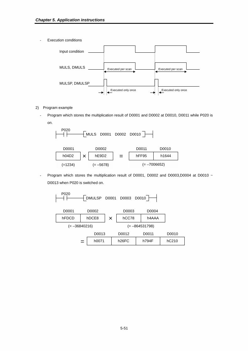
Chapter 5. Application instructions
5-51
� Execution conditions
2) Program example
� Program which stores the multiplication result of D0001 and D0002 at D0010, D0011 while P020 is
on.
� Program which stores the multiplication result of D0001, D0002 and D0003,D0004 at D0010 ~
D0013 when P020 is switched on.
Input condition
MULS, DMULS
MULSP, DMULSP
Executed only once Executed only once
Executed per scan Executed per scan
MULS D0001 D0002 D0010
P020
h04D2 hE9D2 hFF95
D0001
h1644=×D0002 D0011 D0010
DMULSP D0001 D0003 D0010
hFDCD hDCE8 hCC78
D0001
h4AAA
=
×D0002 D0003 D0004
h0071 h26FC
D0013 D0012
h794F hC210
D0011 D0010
P020
(= –7006652)(=1234) (= –5678)
(= –36840216) (= –864531798)

Chapter 5. Application instructions
5-52
5.8.5 DIV, DIVP, DDIV, DDIVP
DIV
(Binary divide)
FUN(124) DIV FUN(126) DDIV
FUN(125) DIVP FUN(127) DDIVP
Applicable
CPUAll CPUs
Available Device FlagInstructions
M P K L F T C S D #D IntegerSteps Error
(F110)Zero
(F111)Carry(F112)
O O O O O O O O O O
O O O O O O O O O ODIV(P)
DDIV(P)O O O O* O O O O
7/9/11 O O
* Available only when do not use computer link module or data link module
1) Functions
� DIV(P) : Performs the division of BIN data specified as [ S1 ] and the BIN data specified as [ S2 ],
and stores the division result into the device specified as [ D+1, D ]. The quotient is stored at [ D ],
and the remainder is stored at [ D+1 ].
� DDIV(P) : Performs the division of BIN data specified as [ S1+1, S ] and the BIN data specified as
[ S2+1, S2 ], and stores the division result into the device specified as [ D+3, D+2, D+1, D ]. The
quotient is stored at [ D+1, D ], and the remainder is stored at [ D+3, D+2 ].
� If the quotient is zero, the zero flag will be set.
� If indirect address specified by #D format is out of device range or the content of divider is 0, the
operation error occurs and the error flag (F110) is set.
� Execution conditions
Operand setting
DIV
DIVP
DDIV
DDIVP
S1
S1
S2
S2
S1
S2
D
D
D
The device storing dividend
The device at which thedivision result is stored
S1
S2
D
The device storing divider
Input condition
DIV, DDIV
DIVP, DDIVP
Executed only once Executed only once
Executed per scan Executed per scan

Chapter 5. Application instructions
5-53
2) Program example
� Program which stores the division result of D0001 and D0002 at D0010, D0011 while P020 is on.
� Program which stores the division result of D0001, D0002 and D0003,D0004 at D0010 ~ D0013
when P020 is switched on.
DIV D0001 D0002 D0010
P020
h78AB h0678 h017D
D0001
h002D=÷D0002 D0011 D0010
DDIVP D0001 D0003 D0010
hF904 h5678 h0021
D0001
h8765
=
÷D0002 D0003 D0004
h0009 hED77
D0013 D0012
h0000 h076D
D0011 D0010
P020
Remainder Quotient
Remainder Quotient

Chapter 5. Application instructions
5-54
5.8.6 DIVS, DIVSP, DDIVS, DDIVSP
DIVS
(Signed binary
divide)
FUN(124) DIV FUN(126) DDIV
FUN(125) DIVP FUN(127) DDIVP
Applicable
CPU
K200S
K300S
K1000S
Available Device FlagInstructions
M P K L F T C S D #D IntegerSteps Error
(F110)Zero
(F111)Carry(F112)
O O O O O O O O O O
O O O O O O O O O ODIVS(P)
DDIVS(P)O O O O* O O O O
7/9/11 O O
* Available only when do not use computer link module or data link module
1) Functions
� DIVS(P) : Performs the division of the signed BIN data specified as [ S1 ] and the signed BIN data
specified as [ S2 ], and stores the division result into the device specified as [ D+1, D ]. The quotient
is stored at [ D ], and the remainder is stored at [ D+1 ].
� DDIVS(P) : Performs the division of the signed BIN data specified as [ S1+1, S ] and the signed BIN
data specified as [ S2+1, S2 ], and stores the division result into the device specified as [ D+3, D+2,
D+1, D ]. The quotient is stored at [ D+1, D ], and the remainder is stored at [ D+3, D+2 ].
� If the quotient is zero, the zero flag will be set.
� If indirect address specified by #D format is out of device range or the content of divider is 0, the
operation error occurs and the error flag (F110) is set.
� The sign of quotient and remainder is as following table;
Quotient Remainder
+ (positive) + (positive) + (positive) + (positive)
+ (positive) – (negative) – (negative) + (positive)
– (negative) + (positive) – (negative) – (negative)
– (negative) – (negative) + (positive) – (negative)
Operand setting
DIVS
DIVSP
DDIVS
DDIVSP
S1
S1
S2
S2
S1
S2
D
D
D
The device storing dividend
The device at which thedivision result is stored
S1
S2
D
The device storing divider
S1 S2

Chapter 5. Application instructions
5-55
� Execution conditions
2) Program example
� Program which stores the division result of D0001 and D0002 at D0010, D0011 while P020 is on.
� Program which stores the division result of D0001, D0002 and D0003,D0004 at D0010 ~ D0013
when P020 is switched on.
Input condition
DIVS, DDIVS
DIVSP, DDIVSP
Executed only once Executed only once
Executed per scan Executed per scan
DIVS D0001 D0002 D0010
P020
h78AB hC678 h059B
D0001
hFFFE=÷D0002 D0011 D0010
DDIVSP D0001 D0003 D0010
hF904 h5678 h0021
D0001
h8765
=
÷D0002 D0003 D0004
hFFF5 h5E61
D0013 D0012
hFFFF hFFCB
D0011 D0010
P020
Remainder Quotient
Remainder Quotient
(= -117156232) (= 2197349)
(= –696735) (= –53)
(= 30891) (= –14728)(= 1435) (= –2)

Chapter 5. Application instructions
5-56
5.9 BCD arithmetic instructions
5.9.1 ADDB, ADDBP, DADDB, DADDBP
ADDB
(BCD addition)
FUN(130) ADDB FUN(132) DADDB
FUN(131) ADDBP FUN(133) DADDBP
Applicable
CPUAll CPUs
Available Device FlagInstructions
M P K L F T C S D #D IntegerSteps Error
(F110)Zero
(F111)Carry(F112)
O O O O O O O O O O
O O O O O O O O O OADDB(P)
DADDB(P)O O O O* O O O O
7/9/11 O O O
* Available only when do not use computer link module or data link module
1) Functions
� ADDB(P) : Performs the addition of 16-bits BCD data specified at [ S1 ] and [ S2 ]. The addition
result is stored at the device specified at [ D ].
� DADDB(P) : Performs the addition of 32-bits BIN data specified at [ S1+1, S1 ] and [ S2+1, S2 ].
The addition result is stored at the device specified at [ D1+1, D1 ].
� When the addition result is over h9999(ADD / ADDP) or h99999999(DADD / DADDP), the carry flag
(F112) is set.
� When the addition result is 0, the zero flag is set.
� If indirect address specified by #D format is out of device range or contents of [ S1 ] and [ S2 ] are
invalid BCD format (out of 0 ~ 9), the operation error occur and the error flag (F110) is set.
Operand setting
ADDB
DADDB
DADDB
DADDBP
The device storing augend
The device at which theaddition result is stored
S1
S1
S2
S2
S1
S2
D
S1
S2
D
D
D
The device storing addend

Chapter 5. Application instructions
5-57
� Execution condition
2) Program example
� When a rising edge is detected at P020, add BCD data of D0000 and D0001 and store the addition
result to P06 word.
Input condition
ADDB, DADDB
ADDBP, DADDBP
Executed only once Executed only once
Executed per scan Executed per scan
ADDP D0000 D0001 P06
16 bits
0 0 1 1 1 0 0 0 1 0 0 1 0 0 1 1
0 0 0 1 0 0 1 0 0 0 0 0 0 1 0 0
+
h3893
h1204
0 1 0 1 0 0 0 0 1 0 0 1 0 1 1 1 h5097
D0000
D0001
P06
P020

Chapter 5. Application instructions
5-58
5.9.2 SUBB, SUBBP, DSUBB, DSUBBP
SUBB
(BCD subtraction)
FUN(134) SUBB FUN(136) DSUBB
FUN(135) SUBBP FUN(137) DSUBBP
Applicable
CPUAll CPUs
Available Device FlagInstructions
M P K L F T C S D #D IntegerSteps Error
(F110)Zero
(F111)Carry(F112)
O O O O O O O O O O
O O O O O O O O O OSUBB(P)
DSUBB(P)O O O O* O O O O
7/9/11 O O O
* Available only when do not use computer link module or data link module
1) Functions
� SUBB(P) : Performs the subtraction of 16-bits BCD data specified at [ S1 ] and [ S2 ]. The
subtraction result is stored at the device specified at [ D ].
� DSUBB(P) : Performs the subtraction of 32-bits BCD data specified at [ S1+1, S1 ] and [ S2+1, S2 ].
The subtraction result is stored at the device specified at [ D1+1, D1 ].
� When the minuend is less than subtrahend, the LSB will underflow, and the carry flag (F112) will be
set.
� When the subtraction result is 0, the zero flag is set.
� If indirect address specified by #D format is out of device range or contents of [ S1 ] and [ S2 ] are
invalid BCD format (out of 0 ~ 9), the operation error occurs and the error flag (F110) is set.
Operand setting
SUBB
SUBBP
DSUBB
DSUBBP
S1
S1
S2
S2
S1
S2
D
D
D
The device storing minuend
The device at which thesubtraction result is stored
S1
S2
D
The device storingsubtrahend
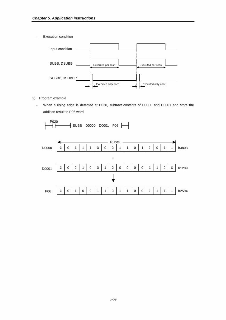
Chapter 5. Application instructions
5-59
� Execution condition
2) Program example
� When a rising edge is detected at P020, subtract contents of D0000 and D0001 and store the
addition result to P06 word.
Input condition
SUBB, DSUBB
SUBBP, DSUBBP
Executed only once Executed only once
Executed per scan Executed per scan
SUBB D0000 D0001 P06P020
16 bits
0 0 1 1 1 0 0 0 1 1 0 1 0 0 1 1
0 0 0 1 0 0 1 0 0 0 0 0 1 1 0 0
-
h3803
h1209
0 0 1 0 0 1 1 0 1 1 0 0 0 1 1 1 h2594
D0000
D0001
P06

Chapter 5. Application instructions
5-60
5.9.3 MULB, MULBP, DMULB, DMULBP
MULB
(BCD multiply)
FUN(140) MULB FUN(142) DMULB
FUN(141) MULBP FUN(143) DMULBP
Applicable
CPUAll CPUs
Available Device FlagInstructions
M P K L F T C S D #D IntegerSteps Error
(F110)Zero
(F111)Carry(F112)
O O O O O O O O O O
O O O O O O O O O OMULB(P)
DMULB(P)O O O O* O O O O
7/9/11 O O
* Available only when do not use computer link module or data link module
1) Functions
� MULB(P) : Performs the multiplication of BCD data specified as [ S1 ] and the BCD data specified
as [ S2 ], and stores the multiplication result into the device specified as [ D+1, D ].
� DMULB(P) : Performs the multiplication of BCD data specified as [ S1+1, S ] and the BCD data
specified as [ S2+1, S2 ], and stores the multiplication result into the device specified as [ D+3, D+2,
D+1, D ]
� If the multiplication result is zero, the zero flag will be set.
� If indirect address specified by #D format is out of device range or contents of [ S1 ] and [ S2 ] is
invalid BCD format (out of 0 ~ 9), the operation error occurs and the error flag (F110) is set.
� Execution conditions
Operand setting
MULB
MULBP
DMULB
DMULBP
S1
S1
S2
S2
S1
S2
D
D
D
The device storingmultiplicand
The device at which themultiplication result isstored
S1
S2
D
The device storing multiplier
Input condition
MULB, DMULB
MULBP, DMULBP
Executed only once Executed only once
Executed per scan Executed per scan

Chapter 5. Application instructions
5-61
2) Program example
� Program which stores the multiplication result of D0001 and D0002 at D0010, D0011 while P020 is
on.
� Program which stores the multiplication result of D0001, D0002 and D0003,D0004 at D0010 ~
D0013 when P020 is switched on.
MULB D0001 D0002 D0010
P020
h1234 h5678 h0700
D0001
h6652=×D0002 D0011 D0010
DMULBP D0001 D0003 D0010
h1234 h5678 h4321
D0001
h8765
=
×D0002 D0003 D0004
h0533 h5649
D0013 D0012
h5624 h7670
D0011 D0010
P020
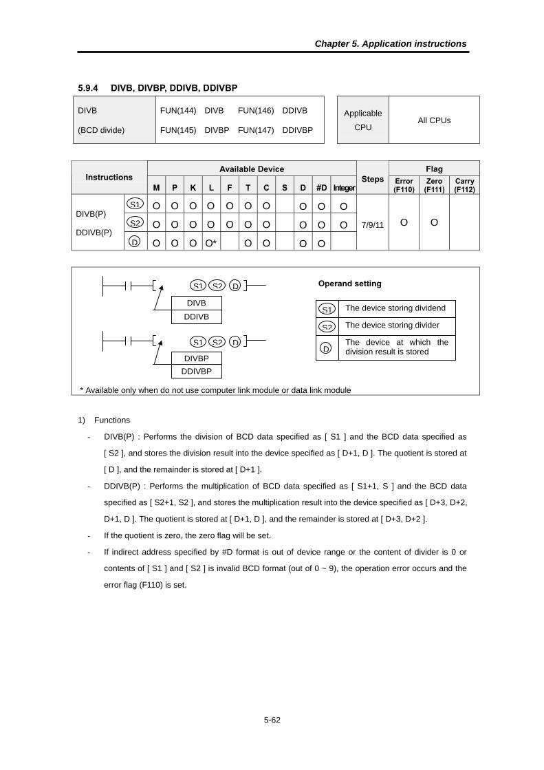
Chapter 5. Application instructions
5-62
5.9.4 DIVB, DIVBP, DDIVB, DDIVBP
DIVB
(BCD divide)
FUN(144) DIVB FUN(146) DDIVB
FUN(145) DIVBP FUN(147) DDIVBP
Applicable
CPUAll CPUs
Available Device FlagInstructions
M P K L F T C S D #D IntegerSteps Error
(F110)Zero
(F111)Carry(F112)
O O O O O O O O O O
O O O O O O O O O ODIVB(P)
DDIVB(P)O O O O* O O O O
7/9/11 O O
* Available only when do not use computer link module or data link module
1) Functions
� DIVB(P) : Performs the division of BCD data specified as [ S1 ] and the BCD data specified as
[ S2 ], and stores the division result into the device specified as [ D+1, D ]. The quotient is stored at
[ D ], and the remainder is stored at [ D+1 ].
� DDIVB(P) : Performs the multiplication of BCD data specified as [ S1+1, S ] and the BCD data
specified as [ S2+1, S2 ], and stores the multiplication result into the device specified as [ D+3, D+2,
D+1, D ]. The quotient is stored at [ D+1, D ], and the remainder is stored at [ D+3, D+2 ].
� If the quotient is zero, the zero flag will be set.
� If indirect address specified by #D format is out of device range or the content of divider is 0 or
contents of [ S1 ] and [ S2 ] is invalid BCD format (out of 0 ~ 9), the operation error occurs and the
error flag (F110) is set.
Operand setting
DIVB
DIVBP
DDIVB
DDIVBP
S1
S1
S2
S2
S1
S2
D
D
D
The device storing dividend
The device at which thedivision result is stored
S1
S2
D
The device storing divider

Chapter 5. Application instructions
5-63
� Execution conditions
2) Program example
� Program which stores the division result of D0001 and D0002 at D0010, D0011 while P020 is on.
� Program which stores the division result of D0001, D0002 and D0003,D0004 at D0010 ~ D0013
when P020 is switched on.
Input condition
DIVB, DDIVB
DIVBP, DDIVBP
Executed only once Executed only once
Executed per scan Executed per scan
DIVB D0001 D0002 D0010
P020
h7806 h0078 h0006
D0001
h0100=÷D0002 D0011 D0010
DDIVBP D0001 D0003 D0010
h3904 h5678 h0001
D0001
h0765
=
÷D0002 D0003 D0004
h0000 h1023
D0013 D0012
h0000 h3627
D0011 D0010
P020
Remainder Quotient
Remainder Quotient

Chapter 5. Application instructions
5-64
5.10 Logical arithmetic instructions
5.10.1 WAND, WANDP, DWAND, DWANDP
WAND
(Word AND)
FUN(150) WAND FUN(152) DWAND
FUN(151) WANDP FUN(153) DWANDP
Applicable
CPUAll CPUs
Available Device FlagInstructions
M P K L F T C S D #D IntegerSteps Error
(F110)Zero
(F111)Carry(F112)
O O O O O O O O O O
O O O O O O O O O OWAND(P)
DWAND(P)O O O O* O O O O
7/9/11 O O
* Available only when do not use computer link module or data link module
1) Functions
� WAND(P) : Performs the logical product of the 16-bit data of device specified at [ S1 ] and [ S2 ] per
bit. Then stores the result of logical production into the device specified at [ D ].
� DWAND(P) : Performs the logical product of the 32-bit data of device specified as [ S1+1, S1 ] and
[ S2+1, S2 ] per bit, and stores the result into the device specified at [ D+1, D ].
� If the result of logical product is 0, the zero flag (F111) is set.
� If the indirect address specified by #D format is out of device range, the operation error occurs and
the error flag (F110) is set.
Operand setting
WAND
WANDP
DWAND
DWANDP
S1
S1
S2
S2
S1
S2
D
D
D
Data for which logicalproduct will be performed
The device at which theresult of logical product isstored
S1
S2
D
16 bits
0 0 1 1 1 0 1 0 1 1 0 1 0 0 1 1
0 0 1 0 0 0 1 0 0 1 0 0 1 1 0 1
AND
h3AD3
h224D
0 0 1 0 0 0 1 0 0 1 0 0 0 0 0 1 h2241
S1
S2
D

Chapter 5. Application instructions
5-65
� Execution conditions
2) Program example
� Program which performs the logical production of the contents of P04 and P05 words, then stores
the result to the P06 word when the P020 is switched on.
Input condition
WAND, DWAND
WANDP, DWANDP
Executed only once Executed only once
Executed per scan Executed per scan
WANDP P04 P05 P06
P020
16 bits
0 0 1 1 1 0 1 0 1 1 0 1 0 0 1 1
0 0 1 0 0 0 1 0 0 1 0 0 1 1 0 1
AND
h3AD3
h224D
0 0 1 0 0 0 1 0 0 1 0 0 0 0 0 1 h2241
h3AD3
P05
P06
P04

Chapter 5. Application instructions
5-66
5.10.2 WOR, WORP, DWOR, DWORP
WOR
(Word OR)
FUN(154) WOR FUN(156) DWOR
FUN(155) WORP FUN(157) DWORP
Applicable
CPUAll CPUs
Available Device FlagInstructions
M P K L F T C S D #D IntegerSteps Error
(F110)Zero
(F111)Carry(F112)
O O O O O O O O O O
O O O O O O O O O OWOR(P)
DWOR(P)O O O O* O O O O
7/9/11 O O
* Available only when do not use computer link module or data link module
1) Functions
� WOR(P) : Performs the logical addition of the 16-bit data of device specified at [ S1 ] and [ S2 ] per
bit. Then stores the result of logical addition into the device specified at [ D ].
� DWOR(P) : Performs the logical addition of the 32-bit data of device specified as [ S1+1, S1 ] and
[ S2+1, S2 ] per bit, and stores the result into the device specified at [ D+1, D ].
� If the result of logical addition is 0, the zero flag (F111) is set.
� If the indirect address specified by #D format is out of device range, the operation error occurs and
the error flag (F110) is set.
Operand setting
WOR
WORP
DWOR
DWORP
S1
S1
S2
S2
S1
S2
D
D
D
Data for which logicaladdition will be performed
The device at which theresult of logical addition isstored
S1
S2
D
16 bits
0 0 1 1 1 0 1 0 1 1 0 1 0 0 1 1
0 0 1 0 0 0 1 0 0 1 0 0 1 1 0 1
WOR
h3AD3
h224D
0 0 1 1 1 0 1 0 1 1 0 1 1 1 1 1 h3ADF
S1
S2
D

Chapter 5. Application instructions
5-67
� Execution conditions
2) Program example
� Program that performs the logical addition of the contents of P04 and P05 words, then stores the
result to the P06 word when the P020 is switched on.
Input condition
WOR, DWOR
WORP, DWORP
Executed only once Executed only once
Executed per scan Executed per scan
WORP P04 P05 P06
P020
16 bits
0 0 1 1 1 0 1 0 1 1 0 1 0 0 1 1
0 0 1 0 0 0 1 0 0 1 0 0 1 1 0 1
WOR
h3AD3
h224D
0 0 1 1 1 0 1 0 1 1 0 1 1 1 1 1 h3ADF
P05
P06
P04

Chapter 5. Application instructions
5-68
5.10.3 WXOR, WXORP, DWXOR, DWXORP
WXOR
(Word exclusive OR)
FUN(160) WXOR FUN(162) DWXOR
FUN(161) WXORP FUN(163) DWXORP
Applicable
CPUAll CPUs
Available Device FlagInstructions
M P K L F T C S D #D IntegerSteps Error
(F110)Zero
(F111)Carry(F112)
O O O O O O O O O O
O O O O O O O O O OWXOR(P)
DWXOR(P)O O O O* O O O O
7/9/11 O O
* Available only when do not use computer link module or data link module
1) Functions
� WXOR(P) : Performs the exclusive OR of the 16-bit data of device specified at [ S1 ] and [ S2 ] per
bit. Then stores the result of logical production into the device specified at [ D ].
� DWXOR(P) : Performs the exclusive OR of the 32-bit data of device specified as [ S1+1, S1 ] and
[ S2+1, S2 ] per bit, and stores the result into the device specified at [ D+1, D ].
� If the result of exclusive OR is 0, the zero flag (F111) is set.
� If the indirect address specified by #D format is out of device range, the operation error occurs and
the error flag (F110) is set.
Operand setting
WXOR
WXORP
DWXOR
DWXORP
S1
S1
S2
S2
S1
S2
D
D
D
Data for which exclusiveOR will be performed
The device at which theresult of exclusive OR isstored
S1
S2
D
16 bits
0 0 1 1 1 0 1 0 1 1 0 1 0 0 1 1
0 0 1 0 0 0 1 0 0 1 0 0 1 1 0 1
WXOR
h3AD3
h224D
0 1 0 1 1 0 0 0 1 0 0 1 1 1 1 0 h589E
S1
S2
D
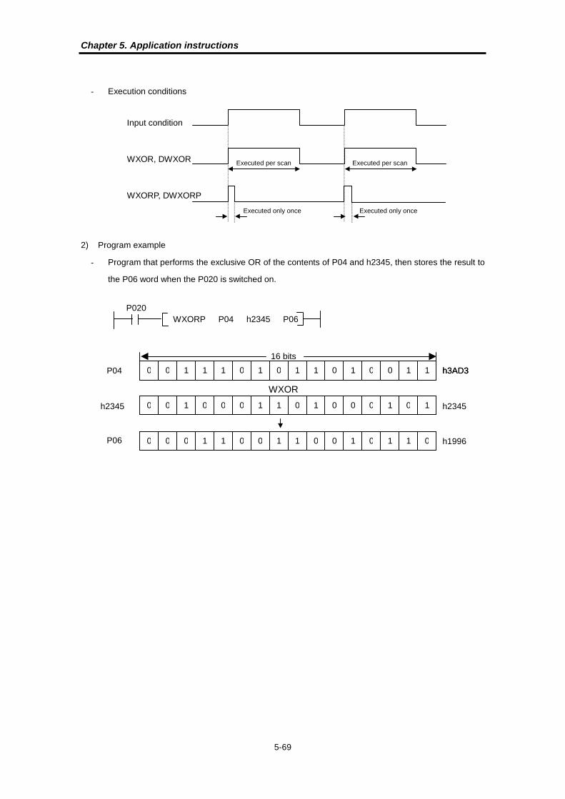
Chapter 5. Application instructions
5-69
� Execution conditions
2) Program example
� Program that performs the exclusive OR of the contents of P04 and h2345, then stores the result to
the P06 word when the P020 is switched on.
Input condition
WXOR, DWXOR
WXORP, DWXORP
Executed only once Executed only once
Executed per scan Executed per scan
WXORP P04 h2345 P06P020
16 bits
0 0 1 1 1 0 1 0 1 1 0 1 0 0 1 1
0 0 1 0 0 0 1 1 0 1 0 0 0 1 0 1
WXOR
h3AD3
h2345
0 0 0 1 1 0 0 1 1 0 0 1 0 1 1 0 h1996
h3AD3
P06
P04
h2345
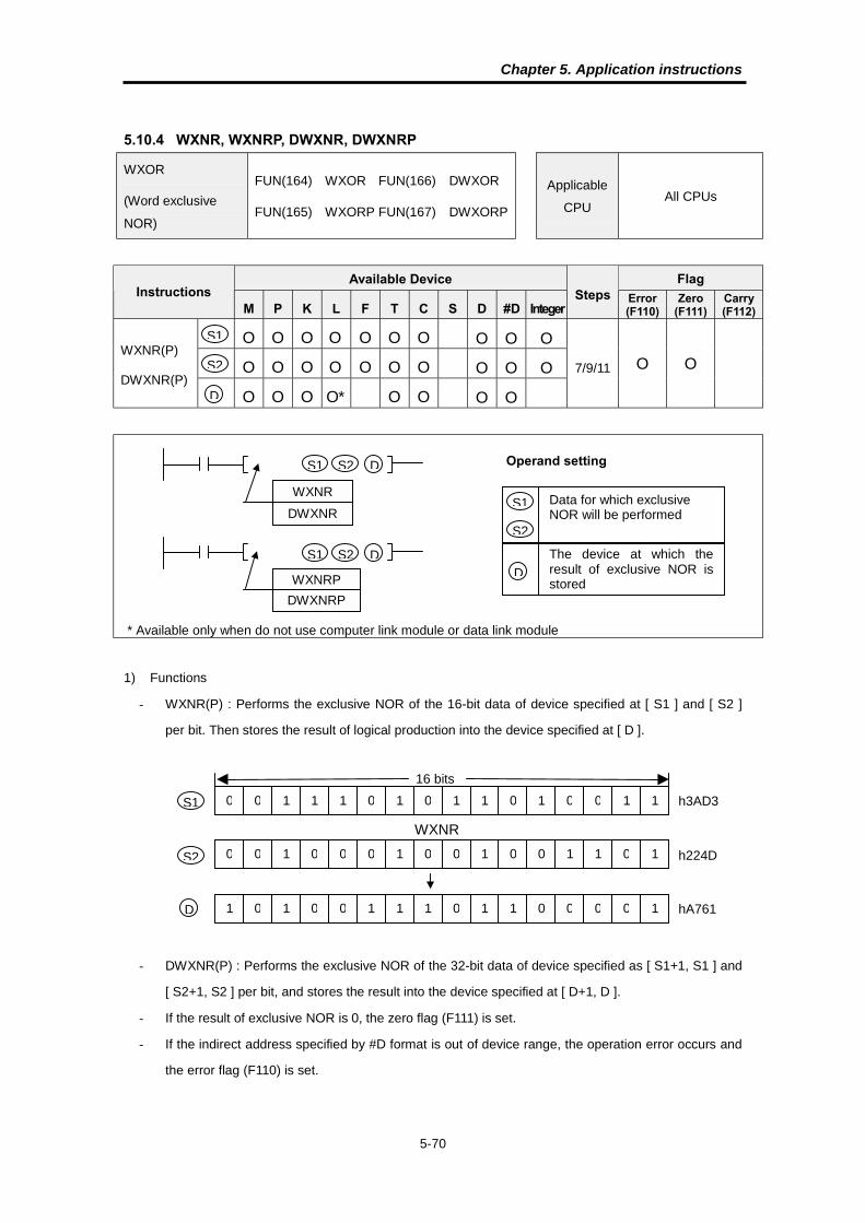
Chapter 5. Application instructions
5-70
5.10.4 WXNR, WXNRP, DWXNR, DWXNRP
WXOR
(Word exclusive
NOR)
FUN(164) WXOR FUN(166) DWXOR
FUN(165) WXORP FUN(167) DWXORP
Applicable
CPUAll CPUs
Available Device FlagInstructions
M P K L F T C S D #D IntegerSteps Error
(F110)Zero
(F111)Carry(F112)
O O O O O O O O O O
O O O O O O O O O OWXNR(P)
DWXNR(P)O O O O* O O O O
7/9/11 O O
* Available only when do not use computer link module or data link module
1) Functions
� WXNR(P) : Performs the exclusive NOR of the 16-bit data of device specified at [ S1 ] and [ S2 ]
per bit. Then stores the result of logical production into the device specified at [ D ].
� DWXNR(P) : Performs the exclusive NOR of the 32-bit data of device specified as [ S1+1, S1 ] and
[ S2+1, S2 ] per bit, and stores the result into the device specified at [ D+1, D ].
� If the result of exclusive NOR is 0, the zero flag (F111) is set.
� If the indirect address specified by #D format is out of device range, the operation error occurs and
the error flag (F110) is set.
Operand setting
WXNR
WXNRP
DWXNR
DWXNRP
S1
S1
S2
S2
S1
S2
D
D
D
Data for which exclusiveNOR will be performed
The device at which theresult of exclusive NOR isstored
S1
S2
D
16 bits
0 0 1 1 1 0 1 0 1 1 0 1 0 0 1 1
0 0 1 0 0 0 1 0 0 1 0 0 1 1 0 1
WXNR
h3AD3
h224D
1 0 1 0 0 1 1 1 0 1 1 0 0 0 0 1 hA761
S1
S2
D

Chapter 5. Application instructions
5-71
� Execution conditions
2) Program example
� Program that performs the exclusive NOR of the contents of P04 and h2345, then stores the result
to the P06 word when the P020 is switched on.
Input condition
WXNR, DWXNR
WXNRP, DWXNRP
Executed only once Executed only once
Executed per scan Executed per scan
WXNRP P04 h2345 P06P020
16 bits
0 0 1 1 1 0 1 0 1 1 0 1 0 0 1 1
0 0 1 0 0 0 1 1 0 1 0 0 0 1 0 1
WXOR
h3AD3
h2345
1 1 1 0 0 1 1 0 0 1 1 0 1 0 0 1 hE669
h3AD3
P06
P04
h2345

Chapter 5. Application instructions
5-72
5.11 Data processing instructions
5.11.1 SEG, SEGP
SEG
(7 segment)
FUN(174) SEG
FUN(175) SEGP
Applicable
CPUAll CPUs
Available Device FlagInstructions
M P K L F T C S D #D IntegerSteps Error
(F110)Zero
(F111)Carry(F112)
O O O O O O O O O
O O O O* O O O OSEG
SEGP
O
7 O
* Available only when do not use computer link module or data link module
1) Functions
� The format of ‘Cw’
a) s : The start bit of [ S ].
b) d : The start bit of [ D ]
c) x : Don’t care
d) x : Numbers of decoded nibbles. (range : 0 ~ F)
� Decodes the data of z�4 bits block that start from the sth bit of device specified at [ S ] into 7
segment display data and stores the result to the z�� bits block that starts from the sth bit of device
[ D ].
Operand setting
SEG
SEGP
S D
S D
The device at which sourcedata is stored
The device which will store7 segment display dataD
D
S
S
Cw
CwInformation for start bit andnumbers of transferred bitsCw
Cw
h s d x z

Chapter 5. Application instructions
5-73
� Execution conditions
2) Program example
� Program that decodes 8-bits from the bit 2 of D0000 into 7 segment display format, and stores the
result to 16-bits from the bit 3 of P06 when P030 is switched on.
Input condition
SEG
SEGP
Executed only once Executed only once
Executed per scan Executed per scan
SEGP D0000 P06 h2302P030
0 0 1 1 1 0 1 0 1 1 0 1 0 0 1 1
1 1 1 0 0 0 1 1 0 0 1 1 0
h3AD3h3AD3P04
0 1 1
D CF E 9 8B A 5 47 6 1 03 2
D CF E 9 8B A 5 47 6 1 03 21 03 2
P07 P06
hB h4
h7C h66
Start from bit 2 ofD0000
Start from bit 3 ofP06 (P063)

Chapter 5. Application instructions
5-74
3) 7 segment display data
Hex Binary
Configuration of 7segment b7 b6 b5 b4 b3 b2 b1 b0
Displayeddata
0 0000 0 0 1 1 1 1 1 1 0
1 0001 0 0 0 0 0 1 1 0 1
2 0010 0 1 0 1 1 0 1 1 2
3 0011 0 1 0 0 1 1 1 1 3
4 0100 0 1 1 0 0 1 1 0 4
5 0101 0 1 1 0 1 1 0 1 5
6 0110 0 1 1 1 1 1 0 1 6
7 0111 0 0 1 0 0 1 1 1 7
8 1000 0 1 1 1 1 1 1 1 8
9 1001 0 1 1 0 1 1 1 1 9
A 1010 0 1 1 1 0 1 1 1 A
B 1011 0 1 1 1 1 1 0 0 B
C 1100 0 0 1 1 1 0 0 1 C
D 1101 0 1 0 1 1 1 1 0 D
E 1110 0 1 1 1 1 0 0 1 E
F 1111 0 1 1 1 0 0 0 1 F
b0
b6b5 b1
b4 b2b3
DS

Chapter 5. Application instructions
5-75
5.11.2 ASC, ASCP
ASC
(ASCII code)
FUN(190) ASC
FUN(191) ASCP
Applicable
CPUAll CPUs
Available Device FlagInstructions
M P K L F T C S D #D IntegerSteps Error
(F110)Zero
(F111)Carry(F112)
O O O O O O O O O
O O O O* O O O OASC
ASCP
O
7 O
* Available only when do not use computer link module or data link module
1) Functions
� The format of ‘Cw’
e) s : The start bit of [ S ].
f) d : The start bit of [ D ]
g) x : Don’t care
h) x : Numbers of decoded nibbles. (range : 0 ~ F)
� Converts the data of z�4 bits block that start from the sth bit of device specified at [ S ] into ASCII
code and stores the result to the z�� bits block that starts from the sth bit of device [ D ].
Operand setting
ASC
ASCP
S D
S D
The device at which sourcedata is stored
The device which will storeASCII dataD
D
S
S
Cw
CwInformation for start bit andnumbers of transferred bitsCw
Cw
h s d x z

Chapter 5. Application instructions
5-76
� Execution conditions
2) Program example
� Program that converts 8-bits from the bit 2 of D0010 into ASCII code data, and stores the result to
16-bits from the bit 1 of P06 while P030 is on.
Input condition
ASC
ASCP
Executed only once Executed only once
Executed per scan Executed per scan
ASC D0010 P06 h2102P030
0 0 1 1 1 0 1 0 1 1 0 1 0 0 1 1
1 0 0 0 0 1 0 0 0 1 1 0 1 0 0
D0010
D CF E 9 8B A 5 47 6 1 03 2
D CF E 9 8B A 5 47 6 1 03 2
P06
hB h4
h42 h34
Start from bit 2 ofD0000
Start from bit 1 ofP06 (P061)
0 0
1 02
P07

Chapter 5. Application instructions
5-77
5.11.3 BSUM, BSUMP, DBSUM, DBSUMP
BSUM
(Bit summary)
FUN(170) BSUM FUN(172) DBSUM
FUN(171) BSUMP FUN(173) DBSUMP
Applicable
CPUAll CPUs
Available Device FlagInstructions
M P K L F T C S D #D IntegerSteps Error
(F110)Zero
(F111)Carry(F112)
O O O O O O O O O OBSUM(P)
DBSUM(P) O O O O* O O O O5 O O
* Available only when do not use computer link module or data link module
1) Functions
� BSUM(P) : Counts the numbers of ‘1’ in the device specified as [ S ], then stores the result into the
device specified as [ D ] in hexadecimal format.
� DBSUM(P) : Counts the numbers of ‘1’ in the device specified as [ S+1, S ], then stores the result
into the device specified as [ D ] in hexadecimal format.
� If the count result is 0, the zero flag is set.
� If the indirect address specified by #D format is out of device range, the operation error occurs and
the error flag (F110) is set.
� Execution conditions
Operand setting
D
S
BSUM
BSUMP
DBSUM
DBSUMP
S D
S D
The device counted thetotal numbers of bits thatare ‘1’.
The device at which storesthe count result.D
S
Input condition
BSUM, DBSUM
BSUMP, DBSUMP
Executed only once Executed only once
Executed per scan Executed per scan

Chapter 5. Application instructions
5-78
2) Program example
� Program that count the numbers of ‘1’ in P020 and P021, then store the count result into D0030
when M020 is switched on.
DBSUMP P020 D0030M020
0 0 1 1 1 0 1 0 1 1 0 1 0 0 1 1P020
D CF E 9 8B A 5 47 6 1 03 2
1 0 1 0 0 0 0 1 1 0 1 1 0 1 1 0P021
D CF E 9 8B A 5 47 6 1 03 2
The numbersof 1 = 9
The numbersof 1 = 8
0 0 0 0 0 0 0 0 0 0 0 1 0 0 0 1D0030
D CF E 9 8B A 5 47 6 1 03 2Total numbers
of 1 = 17(h0011)

Chapter 5. Application instructions
5-79
5.11.4 ENCO, ENCOP
ENCO
(Encode)
FUN(176) ENCO
FUN(177) ENCOP
Applicable
CPUAll CPUs
Available Device FlagInstructions
M P K L F T C S D #D IntegerSteps Error
(F110)Zero
(F111)Carry(F112)
O O O O O O O O O O
O O O O* O O O OENCO
ENCOP
O O
7 O
* Available only when do not use computer link module or data link module
1) Functions
� Encodes the data of 2n bits, which begin the bit 0 of device specified as [ S ], and stores the result
to the device specified as [ D ].
� For ‘n’, 1 ~ 8 can be specified. If the value of n is out of this range, no processing is performed and
the contents of [ D ] is not changed.
� When multiple bits are 1, processing is performed for the most significant bit. If the value of n is 0,
the zero flag (F111) will be set.
� When the value of n is larger than 4, the source data area is expanded like [ S+1 ], [ S+2 ], …
When n=8, the length of source data is 256 bits. ( [ S+15, S+14, …, S+1, S ] )
� Execution conditions
Operand setting
ENCO
ENCOP
S D
S D
The start address of sourcedata area
The start address ofdestination area will storeencoding result
D
D
S
S
n
n
Effective bit length2n ( 1 ~ 8 )
n
n
Input condition
ENCO
ENCOP
Executed only once Executed only once
Executed per scan Executed per scan

Chapter 5. Application instructions
5-80
2) Program example
� Program that encode the 8-bits (bit 0 ~ bit 7) of P06 word and stores the encoding result to the P06
word when P020 is switched on.
� Program that encode the current value of counter C000 and stores the encoding result at the P05
word. The counter C000 is increased at every 1 sec.
ENCOP P02 P06 3
P020
0 0 1 1 1 0 1 0 1 1 0 1 0 0 1 1P02
D CF E 9 8B A 5 47 6 1 03 2The highestposition ‘1’ is
bit 7
0 0 0 0 0 0 0 0 0 0 0 0 0 1 1 1P06
D CF E 9 8B A 5 47 6 1 03 2Encoding
result = h0007
When n = 3,8 (=2n ) bits are effective

Chapter 5. Application instructions
5-81
5.11.5 DECO, DECOP
DECO
(Decode)
FUN(178) DECO
FUN(179) DECOP
Applicable
CPUAll CPUs
Available Device FlagInstructions
M P K L F T C S D #D IntegerSteps Error
(F110)Zero
(F111)Carry(F112)
O O O O O O O O O O
O O O O* O O O ODECO
DECOP
O O
7 O
* Available only when do not use computer link module or data link module
1) Functions
� Decodes the data of lower n bits of the device specified as [ S ], and stores the decoding result to
the block of 2n bits that start from the bit 0 of the device specified as [ D ].
� For ‘n’, 1 ~ 8 can be specified. If the value of n is 0, no processing is performed and the contents of
[ D ] is not changed. If the value of n is over 8, the error flag (F110) is set and no processing is
performed.
� When the value of n is larger than 4, the source data area is expanded like [ D+1 ], [ D+2 ], …
When n=8, the length of decoding result data is 256 bits. ( [ D+15, D+14, …, D+1, D ] )
� Execution conditions
Operand setting
DECO
DECOP
S D
S D
The start address of sourcedata area
The start address ofdestination area will storedecoding result
D
D
S
S
n
n
Effective bit length2n ( 1 ~ 8 )
n
n
Input condition
DECO
DECOP
Executed only once Executed only once
Executed per scan Executed per scan

Chapter 5. Application instructions
5-82
2) Program example
� Program that decode lower 4 bits of p02 word and stores the decoding result to P05 word when
P030 is switched on.
� Program that decodes the current value of counter C000 and stores the decoding result to P05 and
P06 word. The current value of counter is increased at every 1 second and when the current value
reaches to 31, the counter C000 is reset.
DECOP P02 P05 4
P030
F093U CTR C000
R <S> 00031C000
DECO C000 P05 5
F010
END
0 0 0 0 0 0 1 0 0 0 0 0 0 0 0 0P05
D CF E 9 8B A 5 47 6 1 03 2Decoding
result = h0009
When n = 4,16 (=24 ) bits are effective
The value oflast 4 bit ofP02 = h9
0 0 0 0 1 0 0 1 0 1 0 0 1 0 0 1P02
D CF E 9 8B A 5 47 6 1 03 2
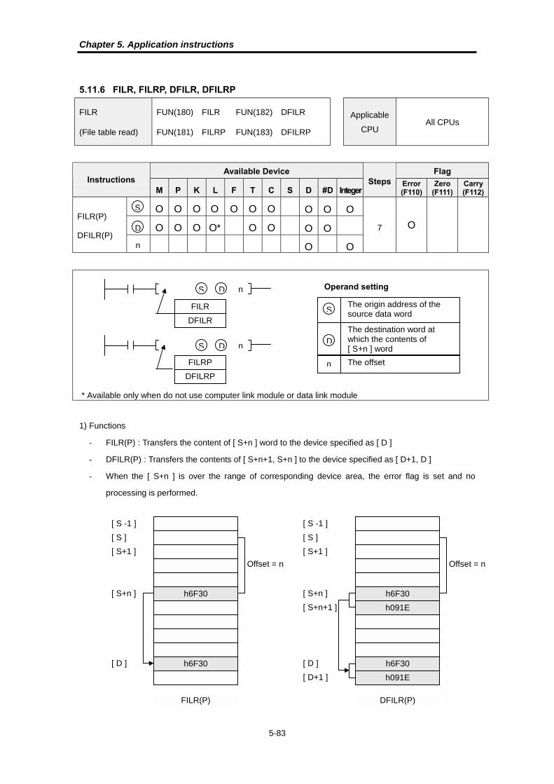
Chapter 5. Application instructions
5-83
5.11.6 FILR, FILRP, DFILR, DFILRP
FILR
(File table read)
FUN(180) FILR FUN(182) DFILR
FUN(181) FILRP FUN(183) DFILRP
Applicable
CPUAll CPUs
Available Device FlagInstructions
M P K L F T C S D #D IntegerSteps Error
(F110)Zero
(F111)Carry(F112)
O O O O O O O O O O
O O O O* O O O OFILR(P)
DFILR(P)
O O
7 O
* Available only when do not use computer link module or data link module
1) Functions
� FILR(P) : Transfers the content of [ S+n ] word to the device specified as [ D ]
� DFILR(P) : Transfers the contents of [ S+n+1, S+n ] to the device specified as [ D+1, D ]
� When the [ S+n ] is over the range of corresponding device area, the error flag is set and no
processing is performed.
Operand setting
FILR
DFILRP
S D
S D
The origin address of thesource data word
The destination word atwhich the contents of[ S+n ] word
D
D
S
S
n
n
The offsetn
n
DFILR
FILRP
h6F30
h6F30
[ S+1 ]
[ S -1 ]
[ S ]
[ S+n ]
[ D ]
Offset = n
FILR(P)
h091E
h6F30
h6F30
h091E
[ S+1 ]
[ S -1 ]
[ S ]
[ S+n ]
[ D ]
Offset = n
[ S+n+1 ]
[ D+1 ]
DFILR(P)

Chapter 5. Application instructions
5-84
� Execution conditions
2) Program example
� Program that transfer the content of the M03+n word to M01 word when P020 is switched on. The n
is stored at D0010 word.
Input condition
FILR, DFILR
FILRP, DFILRP
Executed only once Executed only once
Executed per scan Executed per scan
FILRP M03 M01 D0010P020
h5030
h6030
M002
M000
M001
when n=3
M003
M004
M005
M006
M007
h6030
h5030
h6030
M002
M000
M001
when n=4
M003
M004
M005
M006
M007
h5030

Chapter 5. Application instructions
5-85
5.11.7 FILW, FILWP, DFILW, DFILWP
FILW
(File table write)
FUN(184) FILW FUN(186) DFILW
FUN(185) FILWP FUN(187) DFILWP
Applicable
CPUAll CPUs
Available Device FlagInstructions
M P K L F T C S D #D IntegerSteps Error
(F110)Zero
(F111)Carry(F112)
O O O O* O O O O O
O O O O O O O O OFILW(P)
DFILW(P)
O O
7 O
* Available only when do not use computer link module or data link module
1) Functions
� FILW(P) : Transfers the content of [ S ] word to the device specified as [ D+n ]
� DFILW(P) : Transfers the contents of [ S+1, S ] to the device specified as [ D+n+1, D+n ]
� When the [ D+n ] is over the range of corresponding device area, the error flag is set and no
processing is performed.
Operand setting
FILW
DFILWP
SD
SD
The origin address of thedestination.
The source data or deviceat which the source data isstored
D
D
S
S
n
n
The offsetn
n
DFILW
FILWP
h6F30
h6F30
[ D+1 ]
[ D -1 ]
[ D ]
[ D+n ]
[ S ]
Offset = n
FILW(P)
h091E
h6F30
h6F30
h091E
[ D+1 ]
[ D -1 ]
[ D ]
[ D+n ]
[ S ]
Offset = n
[ D+n+1 ]
[ S+1 ]
DFILW(P)

Chapter 5. Application instructions
5-86
� Execution conditions
2) Program example
� Program that transfer the content of the M01 word to M03+n word when P020 is switched on. The n
is stored at D0010 word.
Input condition
FILW, DFILW
FILWP, DFILWP
Executed only once Executed only once
Executed per scan Executed per scan
FILWP M03 M01 D0010P020
h6030
M002
M000
M001
when n=3
M003
M004
M005
M006
M007
h6030
h6030
M002
M000
M001
when n=4
M003
M004
M005
M006
M007
h6030

Chapter 5. Application instructions
5-87
5.11.8 DIS, DISP
DIS
(Data dissociation)
FUN(194) DIS
FUN(195) DISP
Applicable
CPUAll CPUs
Available Device FlagInstructions
M P K L F T C S D #D IntegerSteps Error
(F110)Zero
(F111)Carry(F112)
O O O O O O O O O
O O O O* O O O ODIS(P)
O O
7 O
* Available only when do not use computer link module or data link module
1) Functions
� Transfers n nibbles that start from the bit 0 of device specified as [ S ] into the lower 4 bits of the
block specified as [ D+n-1 ] ~ [ D ].
� The higher 12 bits (bit 4 ~ bit F) of the block specified as [ D+n-1 ] ~ [ D ] are cleared as 0.
� When n=0, no processing is performed.
� When n > 4, the error flag is set and no processing is performed.
Operand setting
DIS
S D
S D
The source device
The start address ofdestination devices.D
D
S
S
n
n The number of nibble to bedissociated (1 ~ 4)n
n
DISP
When n = 4,16 ( =4�4 ) bits are effective
0 1 0 0 0 0 1 1 0 0 1 0 0 0 0 1
D CF E 9 8B A 5 47 6 1 03 2
0000 0000 0000 0001
0000 0000 0000 0010
0000 0000 0000 0011
0000 0000 0000 0100
D
S
D
D
+1
+2
D +3
F 4 03

Chapter 5. Application instructions
5-88
� Execution conditions
2) Program examples
� Program that dissociate the contents of lower 3 nibbles of P02 word to lower 4 bits of D0000 ~
D0003 when P030 is switched on.
Input condition
DIS
DISP
Executed only once Executed only once
Executed per scan Executed per scan
DISP P02 D0000 3P030
0 1 0 0 0 0 1 1 0 0 1 0 0 0 0 1
D CF E 9 8B A 5 47 6 1 03 2
0000 0000 0000 0001
0000 0000 0000 0010
0000 0000 0000 0011
D0000
D0001
D0002
P02
F 4 03
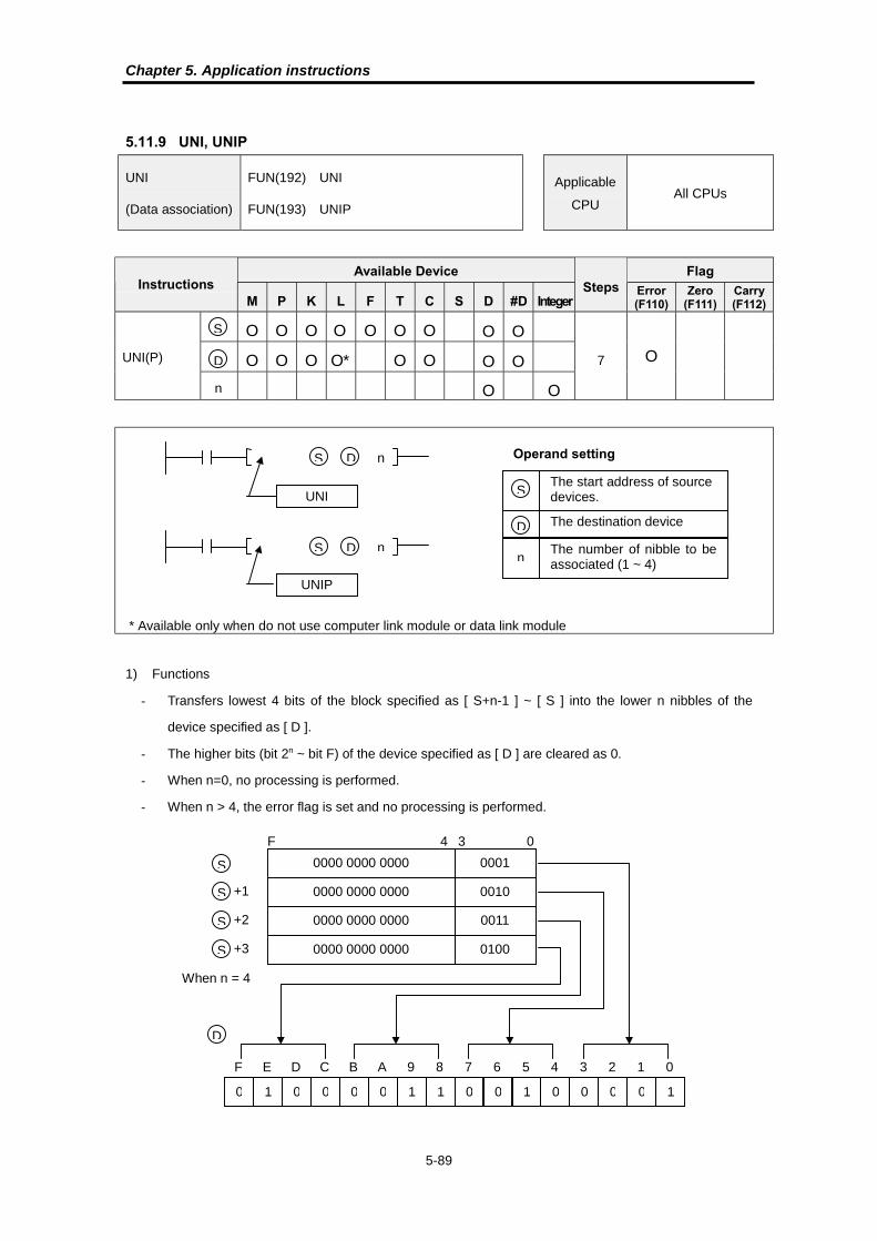
Chapter 5. Application instructions
5-89
5.11.9 UNI, UNIP
UNI
(Data association)
FUN(192) UNI
FUN(193) UNIP
Applicable
CPUAll CPUs
Available Device FlagInstructions
M P K L F T C S D #D IntegerSteps Error
(F110)Zero
(F111)Carry(F112)
O O O O O O O O O
O O O O* O O O OUNI(P)
O O
7 O
* Available only when do not use computer link module or data link module
1) Functions
� Transfers lowest 4 bits of the block specified as [ S+n-1 ] ~ [ S ] into the lower n nibbles of the
device specified as [ D ].
� The higher bits (bit 2n ~ bit F) of the device specified as [ D ] are cleared as 0.
� When n=0, no processing is performed.
� When n > 4, the error flag is set and no processing is performed.
Operand setting
UNI
S D
S D
The destination device
The start address of sourcedevices.
D
D
S
S
n
n The number of nibble to beassociated (1 ~ 4)n
n
UNIP
When n = 4
0 1 0 0 0 0 1 1 0 0 1 0 0 0 0 1
D CF E 9 8B A 5 47 6 1 03 2
0000 0000 0000 0001
0000 0000 0000 0010
0000 0000 0000 0011
0000 0000 0000 0100
S
D
+1
+2
+3
F 4 03
S
S
S

Chapter 5. Application instructions
5-90
� Execution conditions
2) Program examples
� Program that associate the content of lower 4 bits of D0000 ~ D0003 to lower 3 nibbles of P02 word
when P030 is switched on.
Input condition
UNI
UNIP
Executed only once Executed only once
Executed per scan Executed per scan
UNIP D0000 P06 3P030
0 0 0 0 0 0 1 1 0 0 1 0 0 0 0 1
D CF E 9 8B A 5 47 6 1 03 2
0000 0000 0000 0001
0000 0000 0000 0010
0000 0000 0000 0011
D0001
D0002
F 4 03
D0000
P06

Chapter 5. Application instructions
5-91
5.11.10 IORF, IORFP
IORF
(I/O refresh)
FUN(200) IORF
FUN(201) IORFP
Applicable
CPU
K200S
K300S
K1000S
Available Device FlagInstructions
M P K L F T C S D #D IntegerSteps Error
(F110)Zero
(F111)Carry(F112)
OIORF(P)
O5 O
1) Functions
� Refresh I/O data of the block specified as [ D1 ] ~ [ D2 ].
� The [ D1 ] should be lower word than [ D2 ]. If the [ D1 ] is higher than [ D2 ], the error flag is set
and no processing is performed.
� This instruction is useful when read latest input data or output the data of P area to external device
immediately in a sequence program that has a long scan time.
� Execution conditions
Operand setting
The first word of the blockto be refreshed
D1 D2
D1 D2
D1
D2
D1
D2
IORF
IORFP
The last word of the block tobe refreshed
Input condition
IORF
IORFP
Executed only once Executed only once
Executed per scan Executed per scan

Chapter 5. Application instructions
5-92
2) Program example
� During FOR ~ NEXT loop execution, the P060 is keep the initial status, but the P061 is switched
on/off according to the status change of the P020.
( P060 )P020
[ FOR 10000 ]
[ WDT ]F010
[ IORF P02 P02 ]F010
P020( P061 )
[ IORF P06 P06 ]F010
[ NEXT ]
[ END ]
FOR ~ NEXT loop
(Repeats 10000 times)

Chapter 5. Application instructions
5-93
5.12 System instructions
5.12.1 FALS
FALS
(Error display)FUN(204) FALS
Applicable
CPU
K200S
K300S
K1000S
Available Device FlagInstructions
M P K L F T C S D #D IntegerSteps Error
(F110)Zero
(F111)Carry(F112)
FALS O 3
1) Functions
� When the input condition is switched on, stores a number specified as ‘n’ to the F14 word (F140 ~
F14F) and set the FALS flag (F038).
� Once the F14 is set by a FALS instruction, it keeps the value until it is cleared by executing ‘FALS
0000’ instruction. Even if other FALS instruction is executed, the value of F14 word is not changed.
� Execution condition
2) Program example
Operand setting
The error code to be storedat the F area
n
FALS nn
Input condition
FALS Executed per scan Executed per scan
FALS h 1 2 3 4
P030
P031
FALS h A A A A
FALS h B B B B
FALS h 0 0 0 0
P032
P033
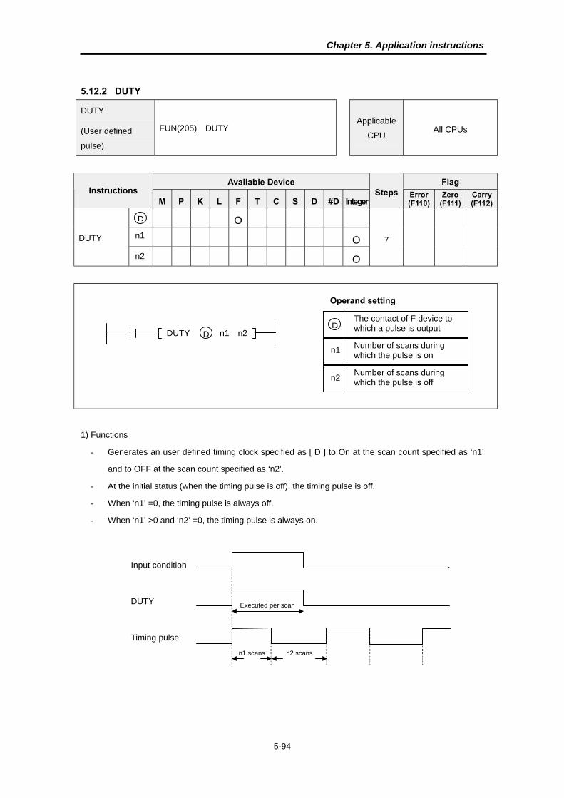
Chapter 5. Application instructions
5-94
5.12.2 DUTY
DUTY
(User defined
pulse)
FUN(205) DUTYApplicable
CPUAll CPUs
Available Device FlagInstructions
M P K L F T C S D #D IntegerSteps Error
(F110)Zero
(F111)Carry(F112)
O
ODUTY
O
7
1) Functions
� Generates an user defined timing clock specified as [ D ] to On at the scan count specified as ‘n1’
and to OFF at the scan count specified as ‘n2’.
� At the initial status (when the timing pulse is off), the timing pulse is off.
� When ‘n1’ =0, the timing pulse is always off.
� When ‘n1’ >0 and ‘n2’ =0, the timing pulse is always on.
Operand setting
The contact of F device towhich a pulse is output
n1
DUTY n1 n2D
n2
D
D
Number of scans duringwhich the pulse is on
Number of scans duringwhich the pulse is off
n1
n2
Input condition
DUTY
Timing pulse
n1 scans
Executed per scan
n2 scans
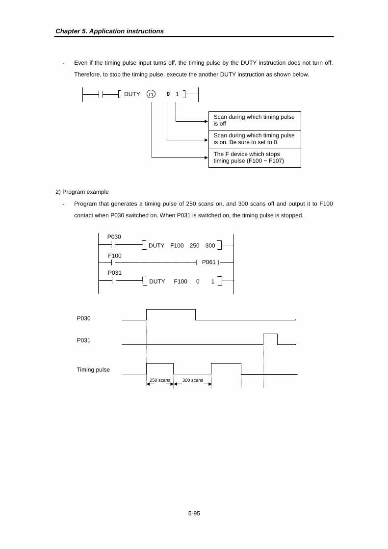
Chapter 5. Application instructions
5-95
� Even if the timing pulse input turns off, the timing pulse by the DUTY instruction does not turn off.
Therefore, to stop the timing pulse, execute the another DUTY instruction as shown below.
2) Program example
� Program that generates a timing pulse of 250 scans on, and 300 scans off and output it to F100
contact when P030 switched on. When P031 is switched on, the timing pulse is stopped.
DUTY 0 1D
Scan during which timing pulseis off
Scan during which timing pulseis on. Be sure to set to 0.
The F device which stopstiming pulse (F100 ~ F107)
DUTY F100 250 300
P030
( P061 )F100
DUTY F100 0 1
P031
P030
Timing pulse
250 scans 300 scans
P031

Chapter 5. Application instructions
5-96
5.12.3 WDT, WDTP
WDT
(Watch dog timer
clear)
FUN(202) WDT
FUN(203) WDTP
Applicable
CPU
K200S
K300S
K1000S
Available Device FlagInstructions
M P K L F T C S D #D IntegerSteps Error
(F110)Zero
(F111)Carry(F112)
WDT
WDTP1
1) Functions
� Resets the watch dog timer in a sequence program
� Used when the period of scan time (from step 0 to END in the sequence program) exceeds the set
value of watch dog timer depending on conditions. If the scan time exceeds the set value of watch
dog timer at every scan, change the set value of watch dog timer by the parameter setting
� Set the set value of the watch dog timer so that ‘t1’ from step 0 to WDT(P) instruction and ‘t2’ from
the WDT(P) to END instruction do not exceed the set value. (See the diagram below)
� The WDT(P) instruction can be user two or more times during one scan. However, please be
careful when use WDT(P) instruction because if an error occurs, the outputs cannot be turned off
immediately.
� Values of scan time stored in special resisters (F device) are not cleared though the WDT(P)
instruction is executed.
WDT
WDTP
t1 t2
WDTPStep 0 END
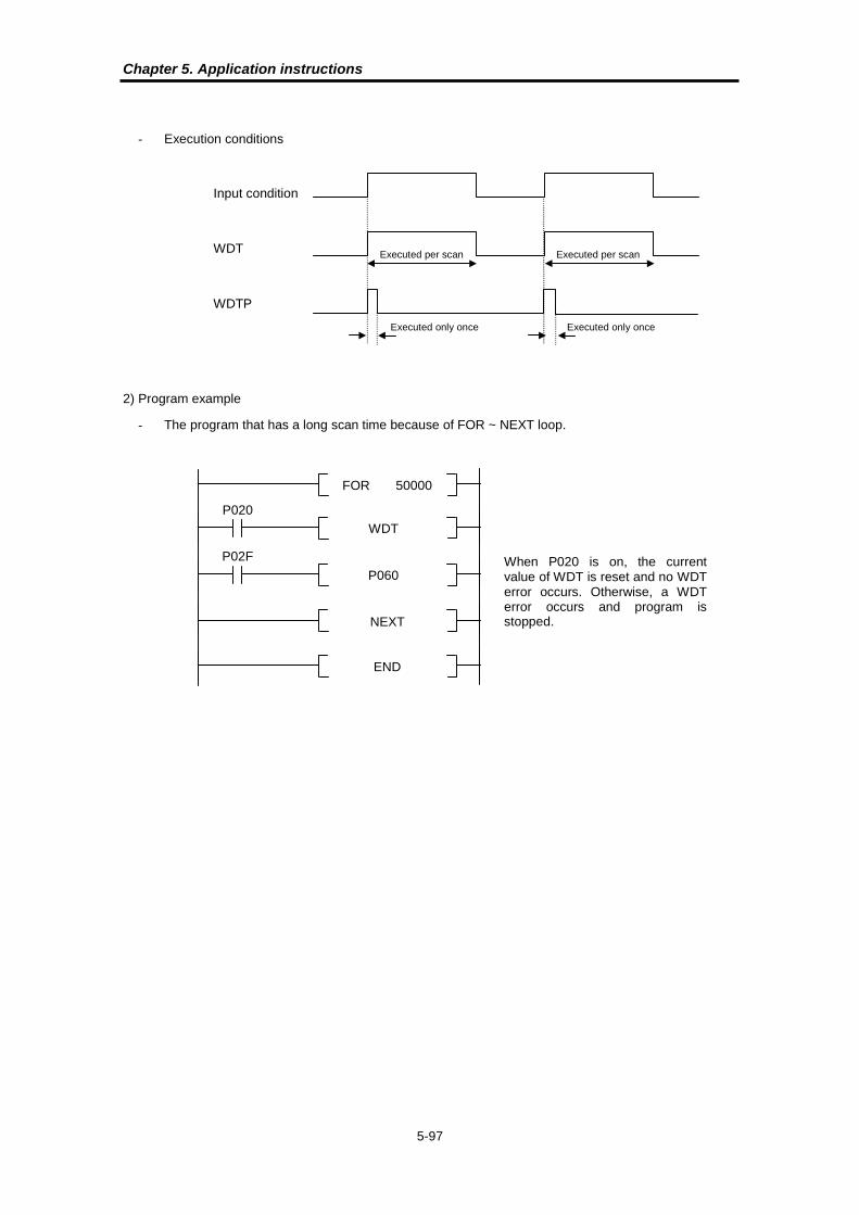
Chapter 5. Application instructions
5-97
� Execution conditions
2) Program example
� The program that has a long scan time because of FOR ~ NEXT loop.
Input condition
WDT
WDTP
Executed only once Executed only once
Executed per scan Executed per scan
FOR 50000
WDT
P060
NEXT
END
P020
P02F When P020 is on, the currentvalue of WDT is reset and no WDTerror occurs. Otherwise, a WDTerror occurs and program isstopped.

Chapter 5. Application instructions
5-98
5.12.4 OUTOFF
OUTOFF
(All output off)FUN(208) OUTOFF
Applicable
CPUAll CPUs
Available Device FlagInstructions
M P K L F T C S D #D IntegerSteps Error
(F110)Zero
(F111)Carry(F112)
OUTOFF 1
1) Functions
� Stops to output the operation result of P area to the external device and turn on the OUTOFF flag
(F113) when an input condition is turns on. However, the P device is updated according to the
operation result.
� When the input condition switched off, the CPU restarts to output operation result of P area to
external devices.
� Useful for test operation of a PLC system.
� Execution conditions
2) Program example
- Program that stop to output to external devices while P020 is on.
OUTOFF
INCP P05
F093
F092
P020
DECP P06
OUTOFF
Input condition
OUTOFF Executed per scan Executed per scan

Chapter 5. Application instructions
5-99
5.12.5 STOP
STOP
(Stop execution of
program)
FUN(008) STOPApplicable
CPU
K200S
K300S
K1000S
Available Device FlagInstructions
M P K L F T C S D #D IntegerSteps Error
(F110)Zero
(F111)Carry(F112)
STOP 1
1) Functions
� When an input condition is switched on, stops execution of sequence program and change mode to
STOP mode after finishing the current scan.
� To resume the operation of CPU after the execution of STOP instruction, change the mode of CPU
to the STOP mode and move it to the RUN mode again by loader or mode switch.
2) Program example
� Program that stops operation when P021 turns on.
STOP
STOP
P021

Chapter 5. Application instructions
5-100
5.13 Branch instructions
5.13.1 JMP, JME
JMP
(Jump)
FUN(012) JMP
FUN(013) JME
Applicable
CPUAll CPUs
Available Device FlagInstructions
M P K L F T C S D #D IntegerSteps Error
(F110)Zero
(F111)Carry(F112)
JMP
JMEO 1
1) Functions
� When the ‘JMP n’ instruction is executed by turn on of input condition, the CPU jumps to the JME
instruction that has same ‘n’ and instructions between ‘JMP n’ and ‘JME n’ are not executed.
� The ‘JMP n’ instruction should be matched only one ‘JME n’ instruction. The duplication of ‘JME n’
is not permitted. However, the duplication of ‘JMP n’ instruction is possible.
� A ‘JMP n’ instruction without corresponding ‘JME n’ instruction (stand-alone ‘JMP n’) will cause
program error. If only a JME or JMP is inside of a loop (subroutine, FOR ~ NEXT, or interrupt
routine), an operation error will occur when the JMP instruction is enabled. (Refer 2.7.1 for details)
JMP
n
JME
n
n
Operand setting
K10S1/K10S/K30S/K60S: 0 ~ 63
K200S/K300S/K1000S : 0 ~ 127
n
JMP 001
JME 001
JME 001
Error
JMP 001
JMP 001
JME 001
No Error
JME 001JME 001

Chapter 5. Application instructions
5-101
� Execution conditions
2) Program example
- Program that skips the ring counter operation between ‘JMP 2’ and ‘JME 2’ when P020 is on.
JMP 02
U CTU C002
R < s > 00100
P030
P031
( P060 )C002
P020
JME 02
Input condition
JMP Executed per scan Executed per scan

Chapter 5. Application instructions
5-102
5.13.2 CALL, CALLP, SBRT, RET
CALL / SBRT
(Subroutine)
FUN(014) CALL FUN(015) CALLP
FUN(016) SBRT FUN(004) RET
Applicable
CPUAll CPUs
Available Device FlagInstructions
M P K L F T C S D #D IntegerSteps Error
(F110)Zero
(F111)Carry(F112)
CALL(P)
SBRTO 1
RET
1) Functions
� When the input condition turns on, stops the sequence program and executes the corresponding
subroutine program specified by pointer ‘n’. After finishing execution of subroutine, resume to
execute sequence program from the next step of ‘CALL n’ instruction.
� Multiple levels of nesting of the CALL(P) instruction are allowed as much as 64.
� The range of pointer ‘n’ is various according to the type of CPU. (See the above picture)
� If a ‘CALL(P) n’ instruction has no corresponding ‘SBRT’ instruction that has same pointer ‘n’ with
the ‘CALL(P) n’ instruction, an instruction error occurs.
� Execution conditions
n
CALL(P) nOperand setting
K10S1 : 0 ~ 15K10S/K30S/K60S
: 0 ~ 63K200S/K300S/K1000S : 0 ~ 127
n
SBRT n
RET
END
Input condition
CALL
CALLP
Executed only once Executed only once
Executed per scan Executed per scan

Chapter 5. Application instructions
5-103
2) Program example
( P050 )P020
( P051 ) P021 P022
CALL 0003P02F
END
SBRT 0003
INCP D0000F092
MOV D0000 P06
F010
RET
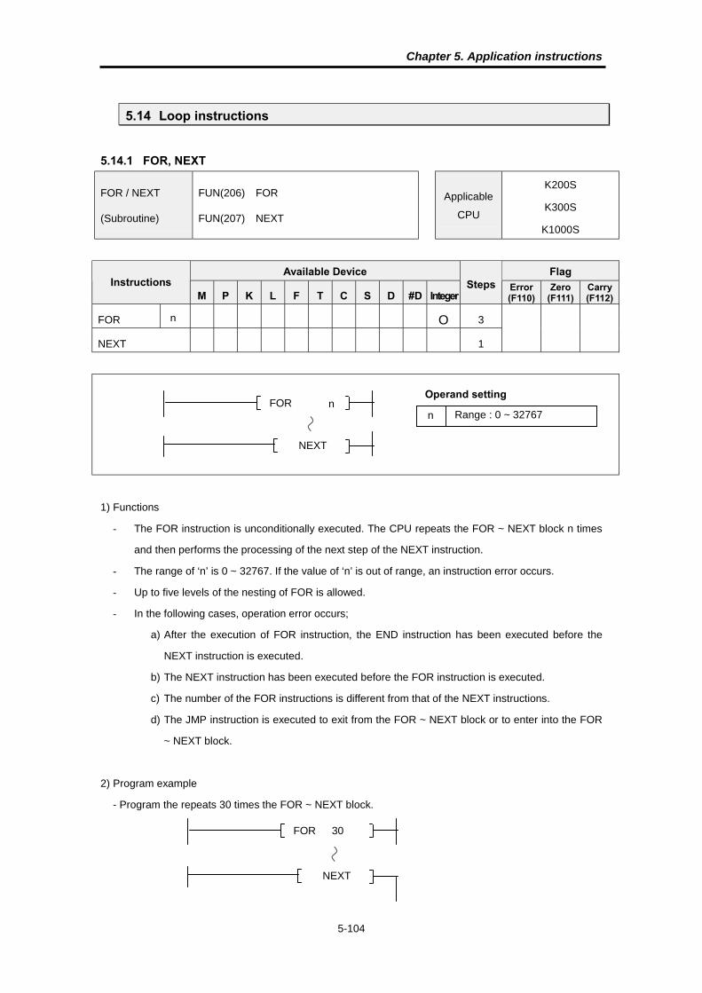
Chapter 5. Application instructions
5-104
5.14 Loop instructions
5.14.1 FOR, NEXT
FOR / NEXT
(Subroutine)
FUN(206) FOR
FUN(207) NEXT
Applicable
CPU
K200S
K300S
K1000S
Available Device FlagInstructions
M P K L F T C S D #D IntegerSteps Error
(F110)Zero
(F111)Carry(F112)
FOR O 3
NEXT 1
1) Functions
� The FOR instruction is unconditionally executed. The CPU repeats the FOR ~ NEXT block n times
and then performs the processing of the next step of the NEXT instruction.
� The range of ‘n’ is 0 ~ 32767. If the value of ‘n’ is out of range, an instruction error occurs.
� Up to five levels of the nesting of FOR is allowed.
� In the following cases, operation error occurs;
a) After the execution of FOR instruction, the END instruction has been executed before the
NEXT instruction is executed.
b) The NEXT instruction has been executed before the FOR instruction is executed.
c) The number of the FOR instructions is different from that of the NEXT instructions.
d) The JMP instruction is executed to exit from the FOR ~ NEXT block or to enter into the FOR
~ NEXT block.
2) Program example
- Program the repeats 30 times the FOR ~ NEXT block.
FOR nOperand setting
Range : 0 ~ 32767n
NEXT
n
FOR 30
NEXT
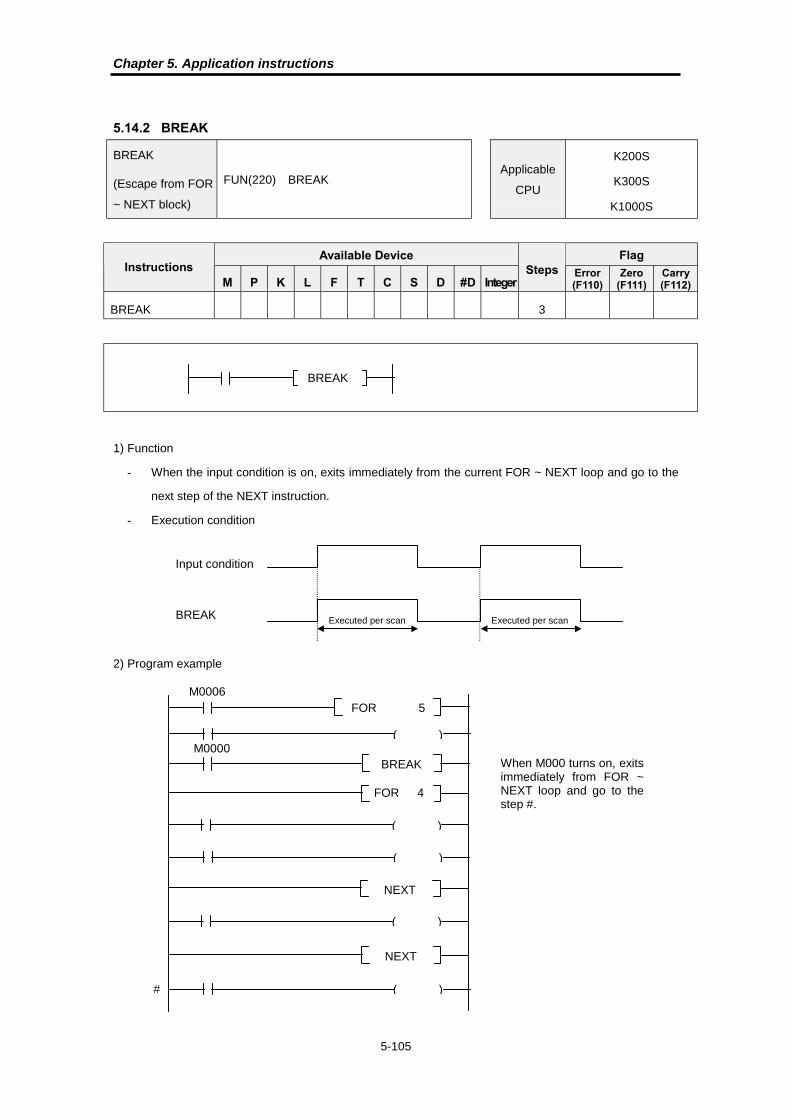
Chapter 5. Application instructions
5-105
5.14.2 BREAK
BREAK
(Escape from FOR
~ NEXT block)
FUN(220) BREAK
Applicable
CPU
K200S
K300S
K1000S
Available Device FlagInstructions
M P K L F T C S D #D IntegerSteps Error
(F110)Zero
(F111)Carry(F112)
BREAK 3
1) Function
� When the input condition is on, exits immediately from the current FOR ~ NEXT loop and go to the
next step of the NEXT instruction.
� Execution condition
2) Program example
BREAK
Input condition
BREAK Executed per scan Executed per scan
M0006
( )
FOR 5
M0000BREAK
FOR 4
( )
( )
NEXT
( )
NEXT
( )#
When M000 turns on, exitsimmediately from FOR ~NEXT loop and go to thestep #.

Chapter 5. Application instructions
5-106
5.15 Flag instructions
5.15.1 STC, CLC
STC, CLC
(Set / Reset the
carry flag)
FUN(002) STC
FUN(003) CLC
Applicable
CPUAll CPUs
Available Device FlagInstructions
M P K L F T C S D #D IntegerSteps Error
(F110)Zero
(F111)Carry(F112)
STC
CLC1 O
1) Functions
� STC : Turns the carry flag (F112) on when the input condition is switched on.
� CLC : Turns the carry flag (F112) off when the input condition is switched on.
� Execution conditions
2) Program example
� Program that set the carry flag (F112) when M0000 is on.
� Program that reset the carry flag (F112) when M0001 is on.
STC
CLC
Input condition
STC, CLC Executed per scan Executed per scan
S T CM0000
C L CM0001

Chapter 5. Application instructions
5-107
5.15.2 CLE
CLE
(Reset the latched
error flag)
FUN(009) CLE
Applicable
CPU
K200S
K300S
K1000S
Available Device FlagInstructions
M P K L F T C S D #D IntegerSteps Error
(F110)Zero
(F111)Carry(F112)
CLE 1
1) Functions
� Reset the latched error flag (F115) when the input condition turns on.
( See the 2.8.2 for detail information of F115 flag)
� Execution condition
2) Program example
- Program that resets the latched error flag (F115) when M0000 turns on.
CLE
Input condition
STC, CLC Executed per scan Executed per scan
CLEM0000

Chapter 5. Application instructions
5-108
5.16 Special module instructions
5.16.1 GET, GETP
GET, GETP
(Read data from
special module)
FUN(230) GET
FUN(231) GETP
Applicable
CPU
K200S
K300S
K1000S
Available Device FlagInstructions
M P K L F T C S D #D IntegerSteps Error
(F110)Zero
(F111)Carry(F112)
O
O
O O O O* O O O OGET(P)
O
9 O
* Available only when do not use computer link module or data link module
1) Functions
� Reads the data of ‘n2’ words, which start at the address specified as [ S ] of buffer memory inside
the special module specified at ‘sl’, and stores the data into devices which begin with the device
specified at [ D ].
D
sl
n2
S
GET sl S D n2
[ S ]
n2 words
The buffer memory ofthe special function
module at the slot ‘sl’
[ D ]
n2 words
CPU module
Operand setting
Slot number of special functionmodule is mounted
Start address of data to be read
Start address of data to be stored
Number of word to be read
sl
S
D
n2

Chapter 5. Application instructions
5-109
� In the following cases, operation error occurs;
a) The slot number specified as ‘sl’ is not a special function module
b) The value of ‘n2’ is over 512, or [ D+n2 ] is exceeds the specified device range.
� Execution conditions
2) Program example
� Program that reads 4 words from the address 0 of buffer memory of A/D module, and stores them
to the 4 words from D0010 of CPU module.
Input condition
GET
GETP
Executed only once Executed only once
Executed per scan Executed per scan
Powersupplymodule
CPUmodule
16 pointsinput
module
32 pointsinput
module
4channel
A/Dmodule
2channel
D/Amodule
slot 0 slot 1 slot 2 slot 3
GET h0002 h0000 D0010 h0004
h0F0F
hE246
h1122
h4477
[ 0 ]
4 words
The buffer memory ofthe A/D module
h4477
h0F0F
h1122D0010
4 words
CPU module
hE246

Chapter 5. Application instructions
5-110
5.16.2 PUT, PUTP
PUT, PUTP
(Write data to
special function
module)
FUN(234) PUT
FUN(235) PUTP
Applicable
CPU
K200S
K300S
K1000S
Available Device FlagInstructions
M P K L F T C S D #D IntegerSteps Error
(F110)Zero
(F111)Carry(F112)
O
O
O O O O* O O O OPUT(P)
O
9 O
* Available only when do not use computer link module or data link module
1) Functions
� Writes the data of ‘n2’ words, which start at the address specified as [ S ] of CPU, and transfer the
data into the block starting at the address specified as [ S ] of buffer memory inside the special
function module mounted at the slot specified as ‘sl’
D
sl
n2
S
PUT sl SD n2
[ S ]
n2 words
The buffer memory of thespecial function module
mounted at slot ‘sl’
[ D ]
n2 words
CPU module
Operand setting
Slot number of special functionmodule is mounted
Start address of data to be stored
Start address of source data
Numbers of word to be written
n1
S
D
n2

Chapter 5. Application instructions
5-111
� In the following cases, operation error occurs;
a) The slot number specified as ‘sl’ is not a special function module
b) The value of ‘n2’ is over 512, or [ D+n2 ] is exceeds the specified device range.
� Execution conditions
2) Program example
� Program that write 4 words from D0010 of CPU module, and stores them to the 4 words from the
address 0 of buffer memory of D/A module.
Input condition
PUT
PUTP
Executed only once Executed only once
Executed per scan Executed per scan
Powersupplymodule
CPUmodule
16 pointsinput
module
32 pointsinput
module
4channel
A/Dmodule
2channel
D/Amodule
slot 0 slot 1 slot 2 slot 3
GET h0003 h0000 D0010 h0004
h0F0F
hE246
h1122
h4477
[ 0 ]
4 words
The buffer memory ofthe D/A module
h4477
h0F0F
h1122D0010
4 words
CPU module
hE246
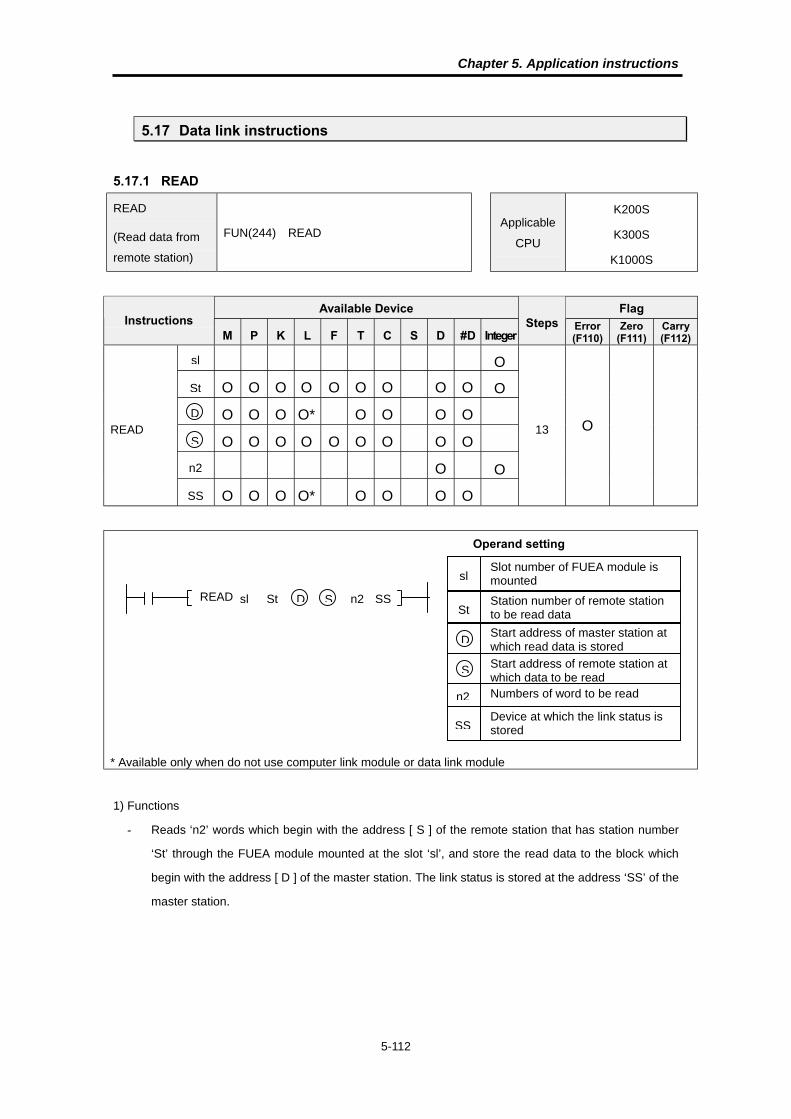
Chapter 5. Application instructions
5-112
5.17 Data link instructions
5.17.1 READ
READ
(Read data from
remote station)
FUN(244) READ
Applicable
CPU
K200S
K300S
K1000S
Available Device FlagInstructions
M P K L F T C S D #D IntegerSteps Error
(F110)Zero
(F111)Carry(F112)
O
O O O O O O O O O O
O O O O* O O O O
O O O O O O O O O
O O
READ
O O O O* O O O O
13 O
* Available only when do not use computer link module or data link module
1) Functions
� Reads ‘n2’ words which begin with the address [ S ] of the remote station that has station number
‘St’ through the FUEA module mounted at the slot ‘sl’, and store the read data to the block which
begin with the address [ D ] of the master station. The link status is stored at the address ‘SS’ of the
master station.
READ St SD n2
Operand setting
Slot number of FUEA module ismounted
Station number of remote stationto be read data
Start address of master station atwhich read data is stored
Start address of remote station atwhich data to be read
sl
S
D
n2
D
sl
n2
S
St
SS
sl SS
Numbers of word to be read
SS
St
Device at which the link status isstored
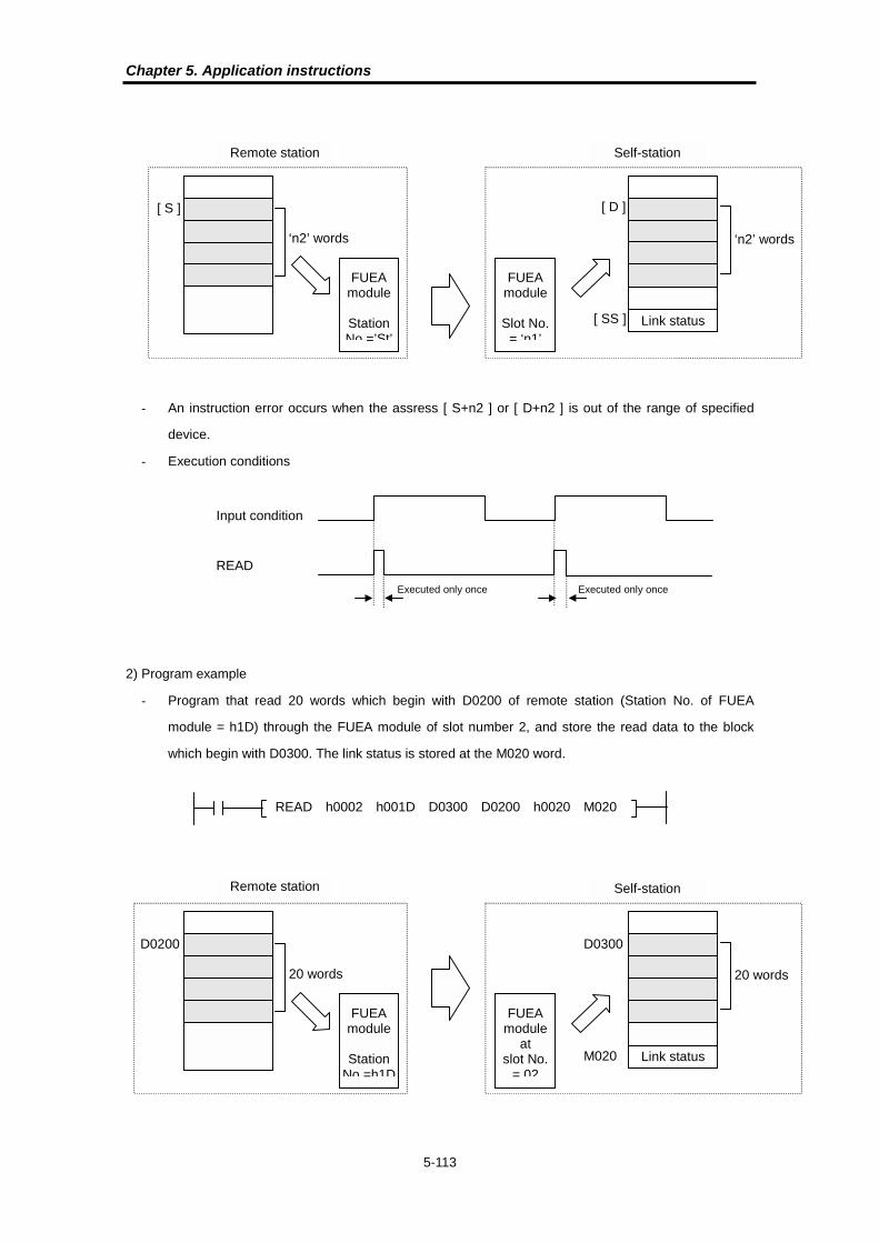
Chapter 5. Application instructions
5-113
� An instruction error occurs when the assress [ S+n2 ] or [ D+n2 ] is out of the range of specified
device.
� Execution conditions
2) Program example
� Program that read 20 words which begin with D0200 of remote station (Station No. of FUEA
module = h1D) through the FUEA module of slot number 2, and store the read data to the block
which begin with D0300. The link status is stored at the M020 word.
Input condition
READ
Executed only once Executed only once
[ S ]
‘n2’ words
Remote station
FUEAmodule
StationNo =’St’
[ D ]
‘n2’ words
Self-station
FUEAmodule
Slot No.= ‘n1’
Link status[ SS ]
READ h0002 h001D D0300 D0200 h0020 M020
D0200
20 words
Remote station
FUEAmodule
StationNo =h1D
20 words
Self-station
FUEAmodule
atslot No.
= 02Link status
D0300
M020

Chapter 5. Application instructions
5-114
Powersupplymodule
CPUmodule
16 pointsinput
module
32 pointsinput
module
4channel
A/Dmodule
FUEAmodule
StationNo h1D
slot 0 slot 1 slot 2 slot 3
Powersupplymodule
CPUmodule
16 pointsinput
module
32 pointsinput
module
4channel
A/Dmodule
FUEAmodule
StationNo h2F
slot 0 slot 1 slot 2 slot 3
Powersupplymodule
CPUmodule
16 pointsinput
module
32 pointsinput
module
FUEAmodule
StationNo h01
FUEAmodule
StationNo h02
slot 0 slot 1 slot 2 slot 3
Self-station
System configuration

Chapter 5. Application instructions
5-115
5.17.2 WRITE
WRITE
(Write data to
remote station)
FUN(245) WRITE
Applicable
CPU
K200S
K300S
K1000S
Available Device FlagInstructions
M P K L F T C S D #D IntegerSteps Error
(F110)Zero
(F111)Carry(F112)
O
O O O O O O O O O O
O O O O* O O O O
O O O O O O O O O
O O
WRITE
O O O O* O O O O
13 O
* Available only when do not use computer link module or data link module
1) Functions
� Reads ‘n2’ words which begin with the address [ S ], and write the read data to the block which
begin with the address [ D ] of the remote station that has a station number specified as ‘St’ through
the FUEA module mounted at the slot ‘sl’ of self station. The link status is stored at the address ‘SS’
of the master station.
WRITE St S D n2
D
sl
n2
S
St
SS
sl SS
Operand setting
Slot number of FUEA module ismounted
Station number of remote stationto be read data
Start address of master station atwhich read data is stored
Start address of remote station atwhich data to be read
sl
S
D
n2 Numbers of word to be read
SS
St
Device at which the link status isstored

Chapter 5. Application instructions
5-116
� An instruction error occurs when the assress [ S+n2 ] or [ D+n2 ] is out of the range of specified
device.
� Execution conditions
2) Program example
� Program that read 14 words which begin with D1234 of self station, and write the read data to the
block which begin with D5678 of remote station (Station No. of FUEA module = h2F) through the
FUEA module at slot number 3 of self station. The link status is stored at the K015 word.
(System configuration is same as the example of READ instruction.)
Input condition
WRITE
Executed only once Executed only once
[ D ]
‘n2’ words
Remote station
FUEAmodule
StationNo =’St’
[ S ]
‘n2’ words
Self-station
FUEAmodule
atslot No.= ‘n1’
Link status[ SS ]
WRITE h0003 h002F D1234 D5678 h0014 K015
D5678
14 words
Remote station
FUEAmodule
StationNo =h1D
14 words
Self-station
FUEAmodule
Slot No.= 02
Link status
D1234
K015

Chapter 5. Application instructions
5-117
5.17.3 RGET
RGET
(Read data from special function
module of remote station)
FUN(232) RGET
Applicable
CPU
K200S
K300S
K1000S
Available Device FlagInstructions
M P K L F T C S D #D IntegerSteps Error
(F110)Zero
(F111)Carry(F112)
O
O
O O O O* O O O O
O
O O
RGET
O O O O* O O O O
13 O
* Available only when do not use computer link module or data link module
1) Functions
� Reads the data of ‘n2’ words, which start at the address specified as [ S ] of buffer memory inside
the special function module of remote station (station number & slot number is specified as ‘St’)
through the FUEA module, and stores the data into devices which begin with the device specified
as [ D ]. Then, stores the link status into the device specified as [ SS ] of self station.
D
sl
n2
S
St
SS
RGET St SD n2sl SS
Operand setting
Slot number of FUEA module ismounted & Type of specialfunction module to be read
Station number of remote stationto be read data & Slot number ofspecial function module
Start address of self station atwhich read data is stored
Start address of remote station atwhich data to be read
sl
S
D
n2 Numbers of word to be read
SS
St
Device at which the link status isstored
Lower 8 bits (CD) : Slot No. of FUEAHigher 8 bits (AB) : Type of special function module
AB CD
The configuration of ‘sl’
Lower 8 bits (CD) : Station No. of remote stationHigher 8 bits (AB) : Slot No. of special function module
AB CD
The configuration of ‘St’
AD DAI TC RTD
K1000S 00h 01h 02h 03h 04h
K300S 80h 81h 82h 83h 84h
K200S 80h 81h 82h − −
DAV
The ID code of special function module
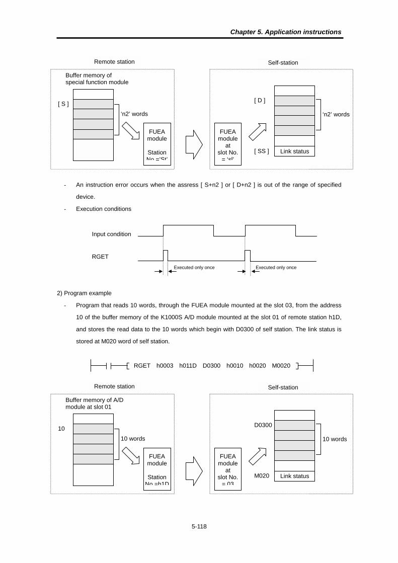
Chapter 5. Application instructions
5-118
� An instruction error occurs when the assress [ S+n2 ] or [ D+n2 ] is out of the range of specified
device.
� Execution conditions
2) Program example
� Program that reads 10 words, through the FUEA module mounted at the slot 03, from the address
10 of the buffer memory of the K1000S A/D module mounted at the slot 01 of remote station h1D,
and stores the read data to the 10 words which begin with D0300 of self station. The link status is
stored at M020 word of self station.
‘n2’ words
Self-station
FUEAmodule
atslot No.
= ‘sl’Link status
[ D ]
[ SS ]
[ S ]
‘n2’ words
Remote station
FUEAmodule
StationNo =’St’
Buffer memory ofspecial function module
Input condition
RGET
Executed only once Executed only once
10 words
Self-station
FUEAmodule
atslot No.
= 03Link status
D0300
M020
10
10 words
Remote station
FUEAmodule
StationNo =h1D
Buffer memory of A/Dmodule at slot 01
RGET h0003 h011D D0300 h0010 h0020 M0020

Chapter 5. Application instructions
5-119
Powersupplymodule
CPUmodule
16 pointsinput
module
4channel
A/Dmodule
32 pointsinput
module
FUEAmodule
StationNo h1D
slot 0 slot 1 slot 2 slot 3
Powersupplymodule
CPUmodule
16 pointsinput
module
32 pointsinput
module
4channel
A/Dmodule
FUEAmodule
StationNo h2F
slot 0 slot 1 slot 2 slot 3
Powersupplymodule
CPUmodule
16 pointsinput
module
32 pointsinput
module
FUEAmodule
StationNo h01
FUEAmodule
StationNo h02
slot 0 slot 1 slot 2 slot 3
Self-station
System configuration
Remote station 1(K1000S)
Remote station 2(K300S)

Chapter 5. Application instructions
5-120
5.17.4 RPUT
RPUT
(Write data to special function
module of remote station)
FUN(233) RPUT
Applicable
CPU
K200S
K300S
K1000S
Available Device FlagInstructions
M P K L F T C S D #D IntegerSteps Error
(F110)Zero
(F111)Carry(F112)
O
O
O
O O O O* O O O O
O O
RPUT
O O O O* O O O O
13 O
* Available only when do not use computer link module or data link module
1) Functions
� Reads the data of ‘n2’ words, which start at the device specified as [ D ], and write the data to the
block which begin with the address specified as [ S ] of buffer memory inside the special function
module of remote station (station number & slot number is specified as ‘St’) through the FUEA
module. Then, stores the link status into the device specified as [ SS ] of self station.
D
sl
n2
S
St
SS
RPUT St S D n2sl SS
Operand setting
Slot number of FUEA module ismounted & Type of specialfunction module to be read
Station number of remote stationto be read data & Slot number ofspecial function module
Start address of self station atwhich source data is stored
Start address of remote station atwhich data to be written
sl
S
D
n2 Numbers of word to be written
SS
St
Device at which the link status isstored
Lower 8 bits (CD) : Slot No. of FUEAHigher 8 bits (AB) : Type of special function module
AB CD
The configuration of ‘sl’
Lower 8 bits (CD) : Station No. of remote stationHigher 8 bits (AB) : Slot No. of special function module
AB CD
The configuration of ‘St’
AD DAI TC RTD
K1000S 00h 01h 02h 03h 04h
K300S 80h 81h 82h 83h 84h
K200S 80h 81h 82h − −
DAV
The ID code of special function module

Chapter 5. Application instructions
5-121
� An instruction error occurs when the assress [ S+n2 ] or [ D+n2 ] is out of the range of specified
device.
� Execution conditions
2) Program example
� Program that reads 15 words from D0200 of self station, then write the data to the 15 words block
which begin with the address 5 of buffer memory of the K300S A/D module mounted at the slot 02
of remote station h2F through the FUEA module at the slot 02. The link status is stored at M020
word of self station.
(System conficuration is same as that of the example of RGET instruction – p115)
‘n2’ words
Self-station
FUEAmodule
atslot No.
= ‘sl’Link status
[ S ]
[ SS ]
[ D ]
‘n2’ words
Remote station
FUEAmodule
StationNo =’St’
Buffer memory ofspecial function module
Input condition
RPUT
Executed only once Executed only once
15 words
Self-station
FUEAmodule
atslot No.
= 03Link status
D0200
M020
05
15 words
Remote station
FUEAmodule
StationNo =h2F
Buffer memory of A/Dmodule at slot 02
RPUT h8002 h022F D0200 h0005 h0015 M020

Chapter 5. Application instructions
5-122
5.17.5 STATUS
STATUS
(Read the link information of
FUEA module of remote station)
FUN(247) STATUS
Applicable
CPU
K200S
K300S
K1000S
Available Device FlagInstructions
M P K L F T C S D #D IntegerSteps Error
(F110)Zero
(F111)Carry(F112)
O
O O O O O O O O O
O O O O* O O O OSTATUS
O O O O* O O O O
9 O
* Available only when do not use computer link module or data link module
1) Functions
� Read the link information (10 words) from the remote station of which station number is ‘St’ through
the FUEA module mounted at the slot number ‘sl’, and stores the information data to the block
begin with the device specified as [ D ]. The link status is stored into the device [ SS ].
� Execution conditions
2) Program example
- Program that reads the information of remote station (station number is stored at D0000) through the
FUEA module of slot 07, and stores the data from D1234. The link status is stored into K015 word.
D
sl
St
SS
STATUS St Dsl SS
Operand setting
Slot number of FUEA module ismounted & Type of specialfunction module to be read
Station number of remote stationto be read data & Slot number ofspecial function module
Start address of remote station atwhich data to be written
sl
D
SS
St
Device at which the link status isstored
Input condition
RPUT
Executed only once Executed only once
STATUS h0007 D0000 D1234 K015
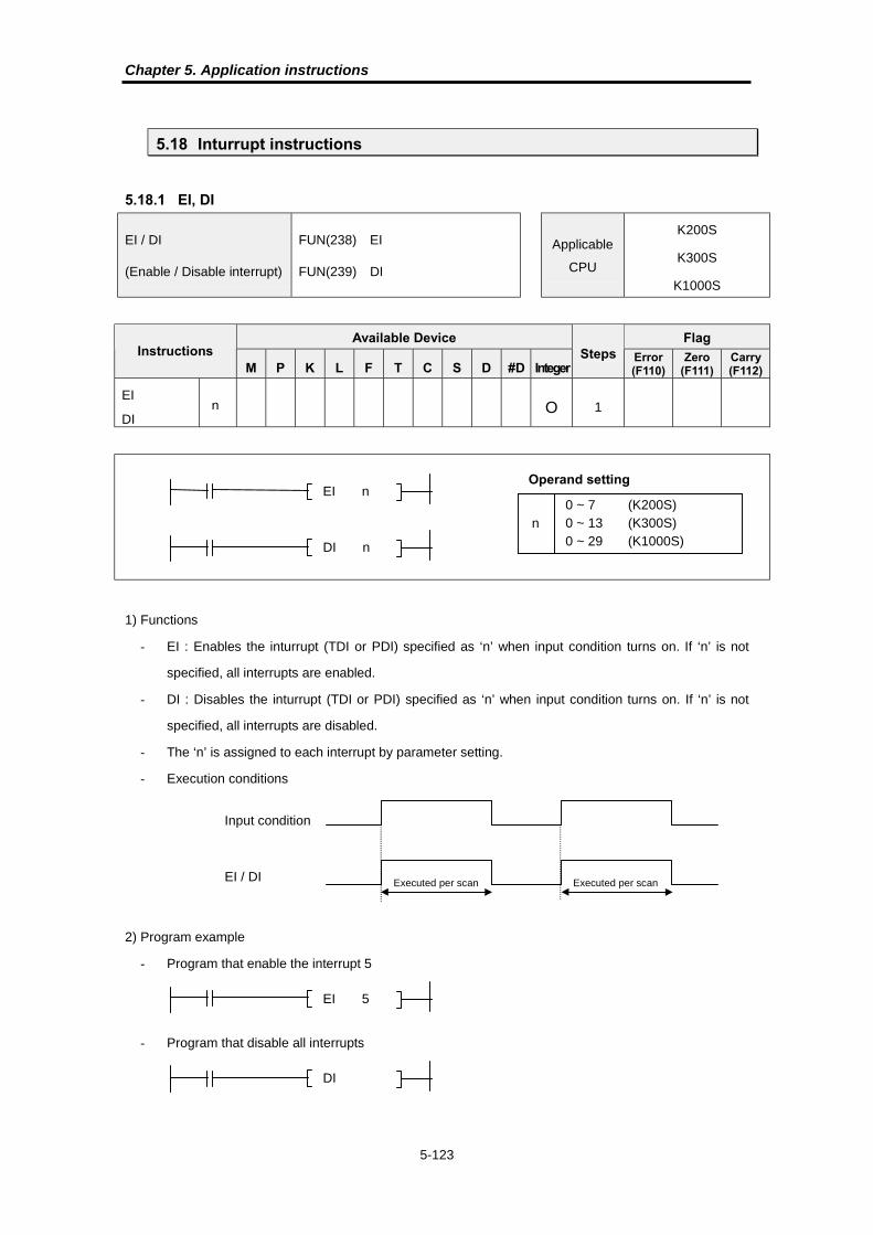
Chapter 5. Application instructions
5-123
5.18 Inturrupt instructions
5.18.1 EI, DI
EI / DI
(Enable / Disable interrupt)
FUN(238) EI
FUN(239) DI
Applicable
CPU
K200S
K300S
K1000S
Available Device FlagInstructions
M P K L F T C S D #D IntegerSteps Error
(F110)Zero
(F111)Carry(F112)
EI
DIO 1
1) Functions
� EI : Enables the inturrupt (TDI or PDI) specified as ‘n’ when input condition turns on. If ‘n’ is not
specified, all interrupts are enabled.
� DI : Disables the inturrupt (TDI or PDI) specified as ‘n’ when input condition turns on. If ‘n’ is not
specified, all interrupts are disabled.
� The ‘n’ is assigned to each interrupt by parameter setting.
� Execution conditions
2) Program example
� Program that enable the interrupt 5
� Program that disable all interrupts
Operand setting
0 ~ 7 (K200S)0 ~ 13 (K300S)0 ~ 29 (K1000S)
n
n
EI n
DI n
EI 5
DI
Input condition
EI / DI Executed per scan Executed per scan

Chapter 5. Application instructions
5-124
5.18.2 TDINT, IRET
TDINT / IRET
(Time driven interrupt)
FUN(226) TDINT
FUN(225) IRET
Applicable
CPU
K200S
K300S
K1000S
Available Device FlagInstructions
M P K L F T C S D #D IntegerSteps Error
(F110)Zero
(F111)Carry(F112)
TDINT O 1
1) Functions
� TDINT : Indicates the begin of the time driven interrupt routine.
� IRET : Indicates the end of the interrupt routine.
� Instructions between the TDINT ‘n’ and the next IRET are executed only when the corresponding
time driven interrupt occurs and is enabled by the EI instruction.
� The interval of interrupt can be set as 60msec ~ 60000msec (unit : 10msec) with parameter setting.
� The execution time of interrupt routine should be less than the interval of interrupt.
� The TDINT n instruction has to be placed after the END instruction.
� The TDINT and IRET instructions are executed unconditionally.
2) Program example
Operand setting
0 ~ 5 (K200S)0 ~ 7 (K300S)0 ~ 15 (K1000S)
n
n
TDINT n
( P0000 )
TDINT n
M0000
•
•
•
•
( P0001 )
IRET
M0001

Chapter 5. Application instructions
5-125
5.18.3 INT, IRET
INT / IRET
(Process driven
interrupt)
FUN(227) INT
FUN(225) IRET
Applicable
CPU
K200S
K300S
K1000S
Available Device FlagInstructions
M P K L F T C S D #D IntegerSteps Error
(F110)Zero
(F111)Carry(F112)
INT O 1
1) Functions
� INT : Indicates the begin of the process driven interrupt routine.
� IRET : Indicates the end of the interrupt routine.
� Instructions between the INT ‘n’ and the next IRET are executed only when the corresponding time
driven interrupt occurs and is enabled by the EI instruction.
� To use process driven interrupts, the interrupt module is required and general input module can not
ube used for interrupt input. However, K200S can use general input module for interrupt input by
parameter setting. (Refer 2.4 ‘Parameter setting’ for details)
� The INT n instruction has to be placed after the END instruction.
� The INT and IRET instructions are executed unconditionally.
2) Program example
Operand setting
0 ~ 5 (K200S)0 ~ 7 (K300S)0 ~ 15 (K1000S)
n
n
INT n
( P0000 )
INT n
M0000
•
•
•
•
( P0001 )
IRET
M0001

Chapter 5. Application instructions
5-126
5.19 Sign inversion instruction
5.19.1 NEG, NEGP, DNEG, DNEGP
NEG
(Sign inverse)
FUN(240) NEG FUN(242) DNEG
FUN(241) NEGP FUN(243) DNEGP
Applicable
CPU
K200S
K300S
K1000S
Available Device FlagInstructions
M P K L F T C S D #D IntegerSteps Error
(F110)Zero
(F111)Carry(F112)
NEG(P)
DNEG(P)O O O O* O O O O 1 O
* Available only when do not use computer link module or data link module
1) Functions
� NEG(P) : Reverses the sign of the 16 bits data of device specified as [ D ] and stores the result in
the device specified as [ D ].
� DNEG(P) : Reversees the sign of the 32 bits data of device specified as [ D+1, D ] and stores the
result in the device specified as [ D+1, D ].
� Used to reverse the positive sign to the negative sign or vice versa.
Operand setting
NEG
NEGP
DNEG
DNEGP
D
D
The device which stores thedata to be inversed.D
D
16 bits0 0 1 1 1 0 1 0 1 1 0 1 0 0 1 1Before execution
D
0 0 1 1 1 0 1 0 1 1 0 1 0 0 1 1
h3AD3
Sign inversion(2’s complement)
1 1 0 0 0 1 0 1 0 0 1 0 1 1 0 1 hC52DAfter execution
D
1 0 0 0 0 0 0 0 0 0 0 0 0 0 0 00
–
= 15059
= –15059
16bits

Chapter 5. Application instructions
5-127
� Execution conditions
2) Program example
� Program that get an absolute value of D0000 when the value of D0000 is negative.
Input condition
NEG, DNEG
NEGP, DNEGP
Executed only once Executed only once
Executed per scan Executed per scan
1 0 1 0 0 0 1 1 0 1 0 0 0 1 0 1 -23739
0 1 0 1 1 1 0 0 1 0 1 1 1 0 1 1 23739D0000
D0000
NEG D0020
< D0020 0000 ( M001A )
M001A
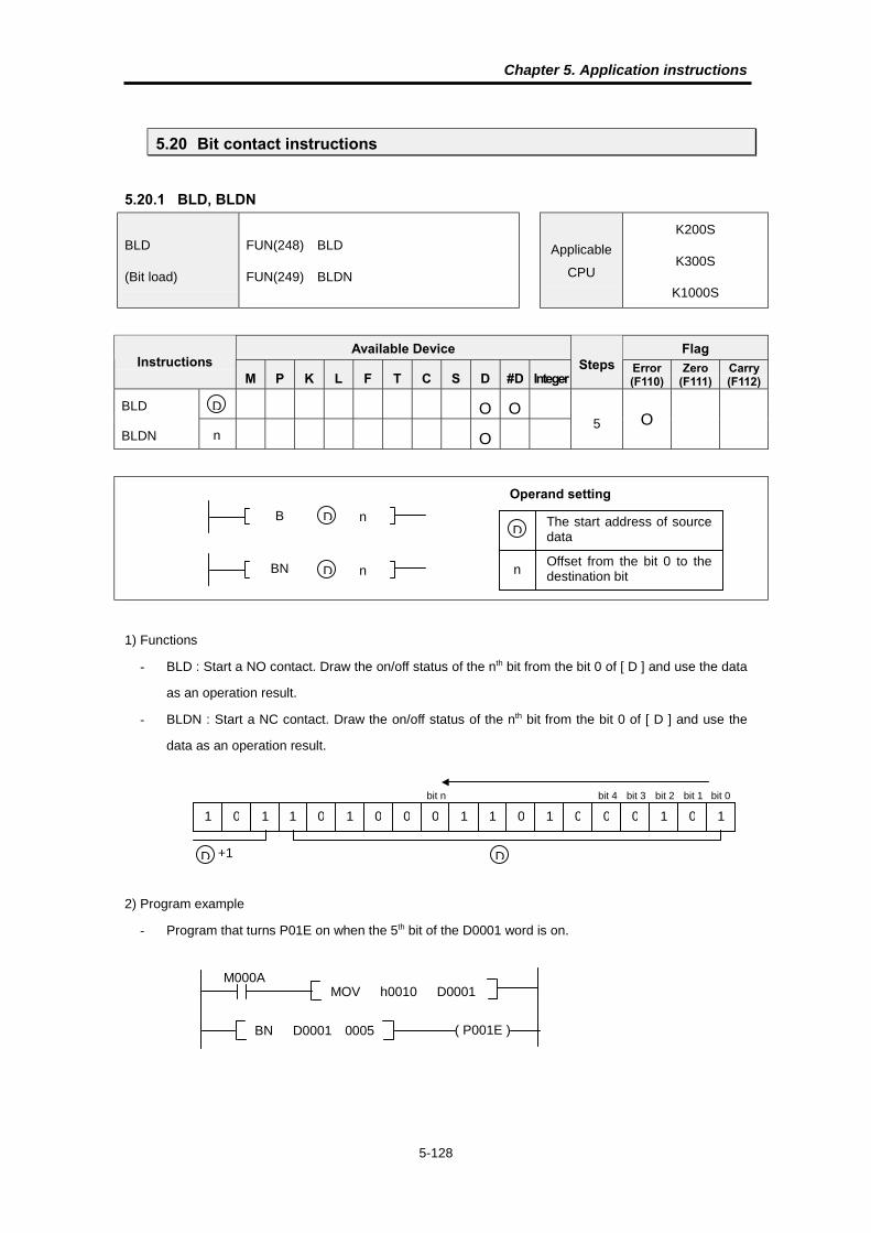
Chapter 5. Application instructions
5-128
5.20 Bit contact instructions
5.20.1 BLD, BLDN
BLD
(Bit load)
FUN(248) BLD
FUN(249) BLDN
Applicable
CPU
K200S
K300S
K1000S
Available Device FlagInstructions
M P K L F T C S D #D IntegerSteps Error
(F110)Zero
(F111)Carry(F112)
O OBLD
BLDN O5 O
1) Functions
� BLD : Start a NO contact. Draw the on/off status of the nth bit from the bit 0 of [ D ] and use the data
as an operation result.
� BLDN : Start a NC contact. Draw the on/off status of the nth bit from the bit 0 of [ D ] and use the
data as an operation result.
2) Program example
� Program that turns P01E on when the 5th bit of the D0001 word is on.
Operand setting
B
BN
D
D
The start address of sourcedataD
n
nOffset from the bit 0 to thedestination bitn
n
D
1 0 1 0 0 0 1 1 0 1 0 0 0 1 0 1
bit 0bit 1bit 2bit 3bit 4bit n
D
1 0 1
D +1
MOV h0010 D0001 M000A
BN D0001 0005 ( P001E )

Chapter 5. Application instructions
5-129
5.20.2 BAND, BANDN
BAND
(Bit AND)
FUN(250) BAND
FUN(251) BANDN
Applicable
CPU
K200S
K300S
K1000S
Available Device FlagInstructions
M P K L F T C S D #D IntegerSteps Error
(F110)Zero
(F111)Carry(F112)
O OBAND
BANDN O5 O
1) Functions
� BAND : A series connection of a NO contact. Reads the on/off status of the nth bit from the bit 0 of
[ D ] and performs the AND operation with previous result, and use it as an new operation result.
� BANDN : A series connection of a NC contact. Reads the on/off status of the nth bit from the bit 0 of
[ D ] and performs the AND operation with previous result, and use it as an new operation result..
2) Program example
� Program that turns on P001A and P001B according to the status of bit 1 and bit 8 of the D0003
word.
Operand setting
B
BN
D
D
The start address of sourcedataD
n
nOffset from the bit 0 to thedestination bitn
n
D
1 0 1 0 0 0 1 1 0 1 0 0 0 1 0 1
bit 0bit 1bit 2bit 3bit 4bit n
D
1 0 1
D +1
MOV h0F0F D0003 M0000
MOV hF0F0 D0003 M0000
B D0003 00001 ( P001A ) M0001
BN D0003 00008 ( P001B )
M0000 P001A P001B
0 0 1
1 1 0
Result (M0001=1)

Chapter 5. Application instructions
5-130
5.20.3 BAND, BANDN
BOR
(Bit OR)
FUN(252) BOR
FUN(253) BORN
Applicable
CPU
K200S
K300S
K1000S
Available Device FlagInstructions
M P K L F T C S D #D IntegerSteps Error
(F110)Zero
(F111)Carry(F112)
O OBOR
BORN O5 O
1) Functions
� BOR : A parallel connection of a NO contact. Reads the on/off status of the nth bit from the bit 0 of
[ D ] and performs the OR operation with previous result, and use it as an new operation result.
� BORN : A parallel connection of a NC contact. Reads the on/off status of the nth bit from the bit 0 of
[ D ] and performs the OR operation with previous result, and use it as an new operation result.
2) Program example
� Program that turns on P0010 and P0011 according to the on/off status of bit 1 and bit 8 of the
D0000 word.
Operand setting
B
BN
D
D
The start address of sourcedataD
n
nOffset from the bit 0 to thedestination bitn
n
D
MOV hFF00 D0000 M0000
( P0010 )M0001
B D0000 0001
( P0011 )
BN D0000 0008
M0001

Chapter 5. Application instructions
5-131
5.20.4 BOUT
BOUT
(Bit output)FUN(236) BOUT
Applicable
CPU
K200S
K300S
K1000S
Available Device FlagInstructions
M P K L F T C S D #D IntegerSteps Error
(F110)Zero
(F111)Carry(F112)
O OBOUT
O5 O
1) Function
� Outputs the current operation result to the the nth bit from the bit 0 of [ D ].
2) Program example
- Program that turns on the bit 2 of D0001 when M0002 is on.
Operand setting
BOUT D The start address of sourcedataD
n
Offset from the bit 0 to thedestination bitn
n
D
BOUT D0001 7
M0002
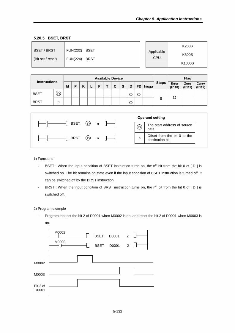
Chapter 5. Application instructions
5-132
5.20.5 BSET, BRST
BSET / BRST
(Bit set / reset)
FUN(232) BSET
FUN(224) BRST
Applicable
CPU
K200S
K300S
K1000S
Available Device FlagInstructions
M P K L F T C S D #D IntegerSteps Error
(F110)Zero
(F111)Carry(F112)
O OBSET
BRST O5 O
1) Functions
� BSET : When the input condition of BSET instruction turns on, the nth bit from the bit 0 of [ D ] is
switched on. The bit remains on state even if the input condition of BSET instruction is turned off. It
can be switched off by the BRST instruction.
� BRST : When the input condition of BRST instruction turns on, the nth bit from the bit 0 of [ D ] is
switched off.
2) Program example
� Program that set the bit 2 of D0001 when M0002 is on, and reset the bit 2 of D0001 when M0003 is
on.
Operand setting
BSET D The start address of sourcedataD
n
Offset from the bit 0 to thedestination bitn
n
D
BRST D n
BSET D0001 2 M0002
BSET D0001 2 M0003
M0002
M0003
Bit 2 ofD0001

Chapter 5. Application instructions
5-133
5.21 Computer link module instructions
5.21.1 SND
SND
(Send data and frame name to
Cnet module)
FUN(169) SND
Applicable
CPU
K200S
K300S
K1000S
Available Device FlagInstructions
M P K L F T C S D #D IntegerSteps Error
(F110)Zero
(F111)Carry(F112)
O
O O O O O O O
O O O O O O O
O O
SND
O O O O O O O
11 O
1) Functions
� Sends ‘n’ bytes which begin with the device specified as [ S ] to the Cnet module that mounted on
the slot ‘sl’. The name of frame is stored as ASCII format into 8 words which begin with the device
[ Fnam ]. The link status is stored at the device specified as [ SS ].
� The maximum size of data block to be sent is 256 bytes.
2) Program example
� Program that send 10 words from D1234 and frame name (8 words from D0000) to the Cnet
module at slot 3, channel 0 (RS232C). The link status is stored at K015 word.
sl
n
S
SS
SND S nsl SS
Operand setting
Slot number of Cnet module ismounted & Type of channel(RS232C or RS422)
The name of frame (8 words)
Start address of device thatstores source data to be sent
sl
S
n Numbers of byte to be sent
SSDevice at which the link status isstored
Lower 8 bits (CD) : Slot No. of Cnetmodule
Higher 8 bits (AB) : Type of channelh00 : RS232Ch01 : RS422
AB CD
The configuration of ‘sl’
Fnam
Fnam
Fnam
SND h0003 D0000 D1234 h0010 K015

Chapter 5. Application instructions
5-134
5.21.2 RCV
RCV
(Receive data and frame name
from Cnet module)
FUN(168) RCV
Applicable
CPU
K200S
K300S
K1000S
Available Device FlagInstructions
M P K L F T C S D #D IntegerSteps Error
(F110)Zero
(F111)Carry(F112)
O
O O O O O O O
O O O O O O O
O O
RCV
O O O O O O O
11 O
1) Functions
� Receives ‘n’ bytes and frame name from the Cnet module that mounted on the slot ‘sl’, then stores
the data from the device specified as [ D ], and frame name as ASCII format into 8 words which
begin with the device [ Fnam ]. The link status is stored at the device specified as [ SS ].
� The maximum size of data block to be sent is 256 bytes.
2) Program example
� Program that receive 20 words and frame name from Cnet module at slot 5, channel 1 (RS232C),
and stores them to the block which begin with D0200 and D0100. The link status is stored at K016
word.
sl
n
D
SS
RCV D nsl SS
Operand setting
Slot number of Cnet module ismounted & Type of channel(RS232C or RS422)
The name of frame (8 words)
Start address of device thatstores source data to be sent
sl
D
n Numbers of byte to be read
SSDevice at which the link status isstored
Lower 8 bits (CD) : Slot No. of Cnetmodule
Higher 8 bits (AB) : Type of channelh00 : RS232Ch01 : RS422
AB CD
The configuration of ‘sl’
Fnam
Fnam
Fnam
RSV h0105 D0100 D0200 h0020 K016
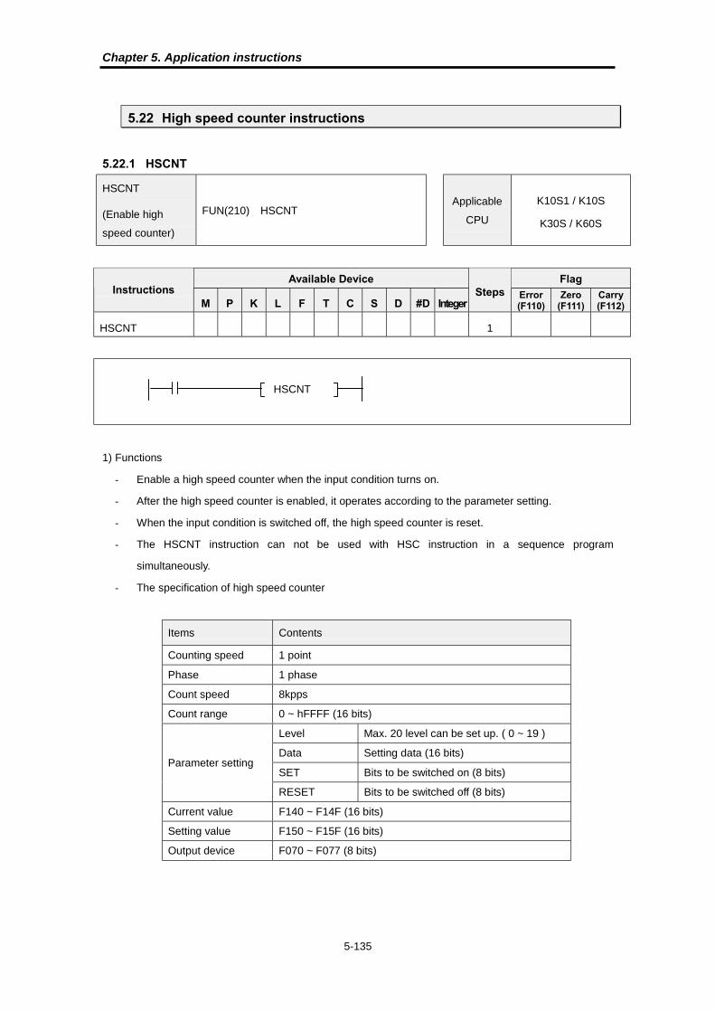
Chapter 5. Application instructions
5-135
5.22 High speed counter instructions
5.22.1 HSCNT
HSCNT
(Enable high
speed counter)
FUN(210) HSCNT
Applicable
CPU
K10S1 / K10S
K30S / K60S
Available Device FlagInstructions
M P K L F T C S D #D IntegerSteps Error
(F110)Zero
(F111)Carry(F112)
HSCNT 1
1) Functions
� Enable a high speed counter when the input condition turns on.
� After the high speed counter is enabled, it operates according to the parameter setting.
� When the input condition is switched off, the high speed counter is reset.
� The HSCNT instruction can not be used with HSC instruction in a sequence program
simultaneously.
� The specification of high speed counter
Items Contents
Counting speed 1 point
Phase 1 phase
Count speed 8kpps
Count range 0 ~ hFFFF (16 bits)
Level Max. 20 level can be set up. ( 0 ~ 19 )
Data Setting data (16 bits)
SET Bits to be switched on (8 bits)Parameter setting
RESET Bits to be switched off (8 bits)
Current value F140 ~ F14F (16 bits)
Setting value F150 ~ F15F (16 bits)
Output device F070 ~ F077 (8 bits)
HSCNT
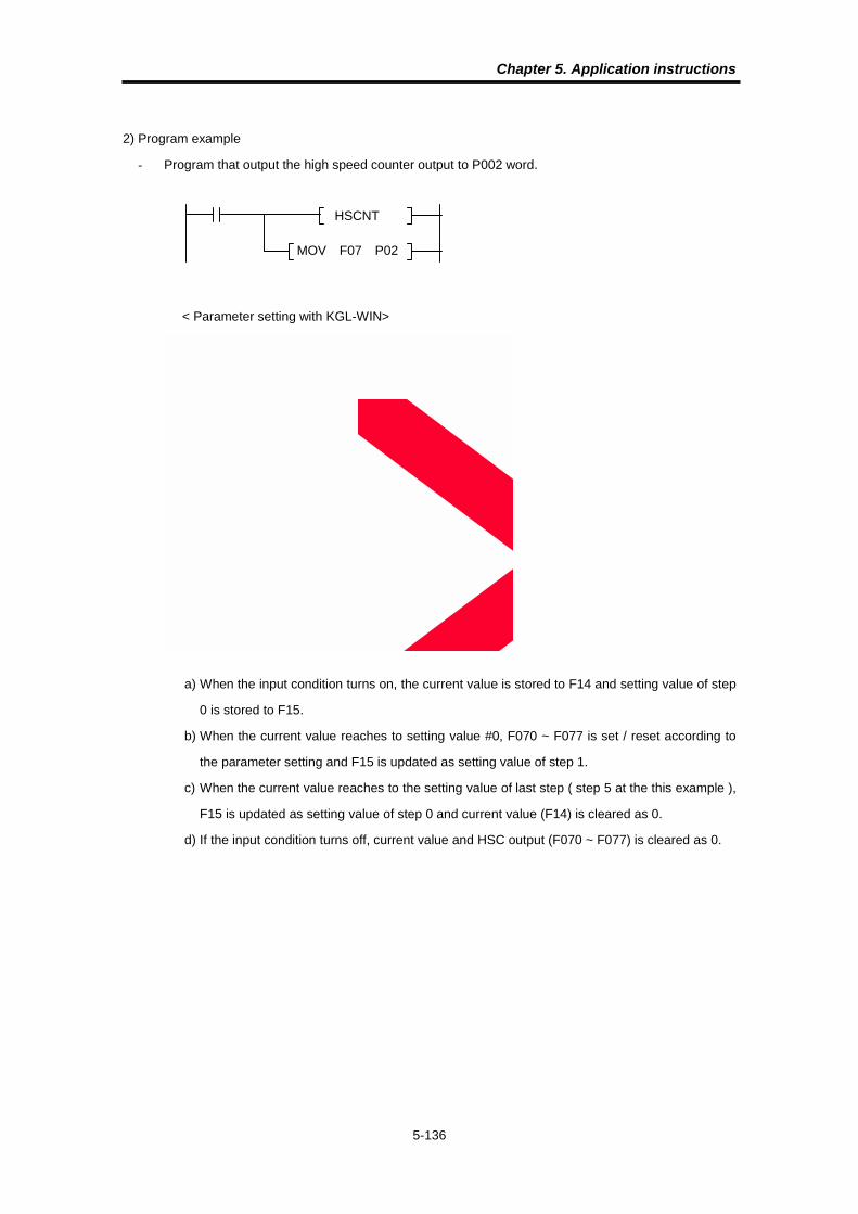
Chapter 5. Application instructions
5-136
2) Program example
� Program that output the high speed counter output to P002 word.
a) When the input condition turns on, the current value is stored to F14 and setting value of step
0 is stored to F15.
b) When the current value reaches to setting value #0, F070 ~ F077 is set / reset according to
the parameter setting and F15 is updated as setting value of step 1.
c) When the current value reaches to the setting value of last step ( step 5 at the this example ),
F15 is updated as setting value of step 0 and current value (F14) is cleared as 0.
d) If the input condition turns off, current value and HSC output (F070 ~ F077) is cleared as 0.
HSCNT
MOV F07 P02
< Parameter setting with KGL-WIN>

Chapter 5. Application instructions
5-137
5.22.2 HSC
HSC
(High speed
counter)
FUN(215) HSC
Applicable
CPU
K10S1 / K10S
K30S / K60S
Available Device FlagInstructions
M P K L F T C S D #D IntegerSteps Error
(F110)Zero
(F111)Carry(F112)
PV O O O O O O O O O OHSC
SV O O O O O O O O O O7/9/11
1) Functions
� HSC instruction can not be used with HSCNT instruction in a program. Only one of them can be
used in a sequence program.
� 32-bits, up / down high speed counter. ( HSCNT : 16-bits, up-counter )
� If the current value same or greater than SV, the HSC output bit (F070) turns on.
� The current value can not be changed by user.
� The current value is stored at F14 (lower word) and F15 (higher word).
� When the HSC instruction is used, the high speed counter parameter setting is ignored.
� Explanation of operands
a) EN : High speed counter enable contact
b) U/D : operates as up counter when U/D is 0, and down counter when U/D is 1.
c) PR : If the PR input turns on, the current value is changed as preset value (PV).
d) PV : Preset value. If the PV is specified as device [ A ], the PV is contents of [ A+1, A ].
e) SV : Setting value. If the SV is specified as device [ A ], the SV is contents of [ A+1, A ].
HSC
EN
U/D
PR
PV < >
SV < >
Operand setting
Preset valuePV
Setting valueSV

Chapter 5. Application instructions
5-138
2) Program example
� M1 : HSC reset, M2 : U/D input (0 = up, 1 = down), M3 : Change current value as PV
� If the current value is same or greater than SV, the F070 bit turns on.
HSC
EN
U/D
PR
PV D010
SV 100
MOV 100 D010M003
M001
M002
M003
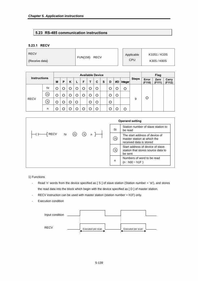
Chapter 5. Application instructions
5-139
5.23 RS-485 communication instructions
5.23.1 RECV
RECV
(Receive data)FUN(158) RECV
Applicable
CPU
K10S1 / K10S
K30S / K60S
Available Device FlagInstructions
M P K L F T C S D #D IntegerSteps Error
(F110)Zero
(F111)Carry(F112)
O O O O O O O O O O
O O O O O O O O O
O O O O O O ORECV
O O O O O O O O O O
9 O
1) Functions
� Read ‘n’ words from the device specified as [ S ] of slave station (Station number = ‘st’), and stores
the read data into the block which begin with the device specified as [ D ] of master station.
� RECV instruction can be used with master station (station number = h1F) only.
� Execution condition
Operand setting
Station number of slave station tobe read
The start address of device ofmaster station at which thereceived data is stored
Start address of device of slavestation that stores source data tobe sent
St
S
nNumbers of word to be read(n : h00 ~ h1F )
St
n
S
D
RECV S nSt D
D
Input condition
RECV Executed per scan Executed per scan
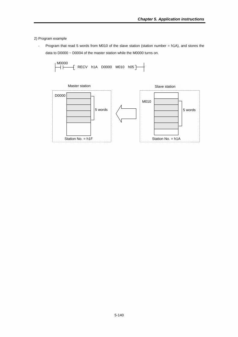
Chapter 5. Application instructions
5-140
2) Program example
� Program that read 5 words from M010 of the slave station (station number = h1A), and stores the
data to D0000 ~ D0004 of the master station while the M0000 turns on.
M0000RECV h1A D0000 M010 h05
5 words
Slave station
M010
Station No. = h1A
D0000
5 words
Master station
Station No. = h1F
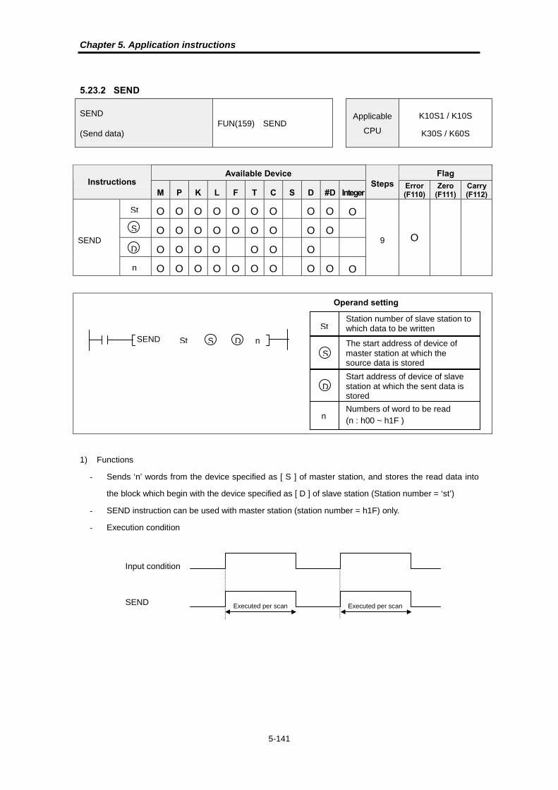
Chapter 5. Application instructions
5-141
5.23.2 SEND
SEND
(Send data)FUN(159) SEND
Applicable
CPU
K10S1 / K10S
K30S / K60S
Available Device FlagInstructions
M P K L F T C S D #D IntegerSteps Error
(F110)Zero
(F111)Carry(F112)
O O O O O O O O O O
O O O O O O O O O
O O O O O O OSEND
O O O O O O O O O O
9 O
1) Functions
� Sends ‘n’ words from the device specified as [ S ] of master station, and stores the read data into
the block which begin with the device specified as [ D ] of slave station (Station number = ‘st’)
� SEND instruction can be used with master station (station number = h1F) only.
� Execution condition
Operand setting
Station number of slave station towhich data to be written
The start address of device ofmaster station at which thesource data is stored
Start address of device of slavestation at which the sent data isstored
St
D
nNumbers of word to be read(n : h00 ~ h1F )
St
n
D
S
SEND D nSt S
S
Input condition
SEND Executed per scan Executed per scan

Chapter 5. Application instructions
5-142
2) Program example
� Program that send 5 words from D0010 of the master station, and stores the data to M0000 ~
M0004 of the slave station (station number = h0A) while the M0000 turns on.
M0000SEND h0A D0010 M000 h05
5 words
Slave station
M000
Station No. = h0A
D0010
5 words
Master station
Station No. = h1F

Appendix
A.1 Memory configuration........................................................................... 1
A.2 Special relay ........................................................................................ 3
A.2 Instruction list ..................................................................................... 12
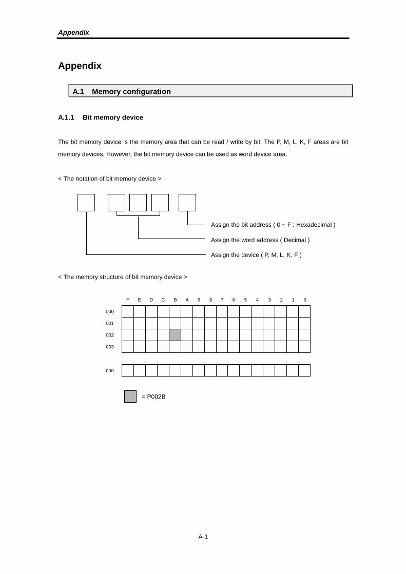
Appendix
A-1
Appendix
A.1 Memory configuration
A.1.1 Bit memory device
The bit memory device is the memory area that can be read / write by bit. The P, M, L, K, F areas are bit
memory devices. However, the bit memory device can be used as word device area.
< The notation of bit memory device >
< The memory structure of bit memory device >
Assign the bit address ( 0 ~ F : Hexadecimal )
Assign the word address ( Decimal )
Assign the device ( P, M, L, K, F )
F E D C B A 9 8 7 6 5 4 3 2 1 0
000
001
002
003
nnn
= P002B

Appendix
A-2
A.1.2 Bit / Word memory device ( timer & counter )
The timer and counter memory area consist of 3 parts - the output bit, current value word, and setting
value word. When the T or C device is used as a operand of bit instruction, the instruction takes effect to
the output bit of timer or counter. If the T or C device is used as an operand of word instruction, the current
value word is effected by the instruction. The setting value can not be changed by user.
A.1.3 Word memory device
The D device used by word. Therefore, the D device can not be used as an operand of bit instruction such
as LOAD, OUT, etc. To control the D device by bit, use special instructions such as BLD, BAND, BOR, etc.
F E D C B A 9 8 7 6 5 4 3 2 1 0
D0000
D0001
D0002
D0003
Dnnnn
= D0002

Appendix
A-3
A.2 Special relay
A.2.1 K10S1 / K10S / K30S / K60S
1) F device
Relay Name Description
F000 Run flag Set while PLC is on RUN modeF001 PGM flag Set while PLC is on PGM modeF002 Pause flag Set while PLC is on Pause modeF007 EPROM mode Set when PLC is on EPROM run mode.F010 Always onF011 Always off
Used as a dummy relay or initalization in user programs
F012 1 scan On On during the first scan after PGM�RUN modeF013 1 scan Off Off during the first scan after PGM�RUN mode
F014Turnover perEach scan
Repeat set/reset during PLC is on RUN mode
F020�
F02F
CommunicationError information
! Replated to SEND, RECV instructions only! Upper byte:The station No. where error occurred Lower byte:error code! The error code of time out error:h20! No error:h000
F030 Serious error Set in case of internal ROM error, 24V fail error
F031 Light errorSet in case of WDT error, program error, I/O combination error,missing END/RET error
F03A RTC data error flag Set when an error is detected in RTC data
F040�
F045I/O combination error
Set in case of attachment/detachment of I/O unitDuring operation, or improper connection
F050�
F05FError code
! h0000:No error ! h0023:Code error! h0014:I/O error ! h0024:Missing END error! h0021:Parameter error! h0025:Missing RET error
F060�
F06F
The step No. Whereerror occurred
! The step No. where program error occurred is stored! In case of branch instruction error, the destination step No. is stored.
F070�
F077HSC register High speed counter area
F080�
F08FPLC model
! K10S:h0031! K60S:h0036! K30S:h0033!K100S:h0035
Upper byte:PLC station No.Lower byte:PLC model

Appendix
A-4
Relay Name Description
F090 20msec period clock
F091 100msec period clock
F092 200msec period clock
F093 1sec period clock
F094 2sec period clock
F095 10sec period clock
F096 20sec period clock
F097 1minute period clock
These relays repeat On/Off with fixed time interval,
and are generated in RUN mode only.
F100
~
F107
User defined clock
F100:clock0
~
F107:clock7
These relays repeat On/Off based on a scan time.
(Initial state=Off)
F110 Arithmetic error flag Set when an arithmetic error occurred during operation
F111 Zero flag Set when the result value is zero
F112 Carry flagSet when Carry or Borrow occurs as a result of
operation
F11A On sending flag
F11C On receiving flag
F11EReceive completion
Flag
These relays indicate the communication status
When DIN, DOUT instruction are used.
F11FCommunication
error flag
! DIN, DOUT:Set when time-out error occurred
! SEND, RECV:Set when time-out error occurs or
NAK massage is detected.
F120 �
F121 �
F122 =
F123 >
F124 �
F125 �
These relays are set according to the result of
Compare instructions
(CMP, CMPP, DCMP, DCMPP)
F130
~
F135
I/O statusEach relays show whether relevant I/O modules
Are attached or not.
F140
~
F14F
HSC present value
HSCNT : The present value of high speed counter is stored.
HSC : The low word of present value of high speed counter is
stored.
F150
~
F15F
HSC preset value
HSCNT : The preset value of high speed counter is stored.
HSC : The high word of present value of high speed counter is
stored.
F094
1sec 1sec
2sec
n1 n2
DUTY F10X n1 n2

Appendix
A-5
2) Other special relays
Area Description Remarks
M310 RTC User Write Enable
When M310 is On, theData of RTC is changedAs the data ofD249~D252
L12~
L15RTC Data
D240 Data of A/D Ch.0 Input
D241 Data of A/D Ch.1 Input
D242
AnalogUnit#1 Data of D/A Output
D243 Data of A/D Ch.0 Input
D244 Data of A/D Ch.1 Input
D245
AnalogUnit#1 Data of D/A Output
D247 High Speed Counter Mode Set Area
K30S-A / K60S-A type
Only
D248Time out Value of RS485Communications
O/S V1.5 or later
D249~
D252RTC User Write Data Area
MK-S Series Ver1.3 orLater Used when M310Point is on Same format
As L12~L15
D253 Current Scan Time
D254 Minimum Scan Time
D255 Maximum Scan Time

Appendix
A-6
A.2.2 K200S / K300S / K1000S
1) F relay
Contact Keyword Function DescriptionF0000 RUN mode Turns on when the CPU in the RUN mode.F0001 Program mode Turns on when the CPU in the Program modeF0002 Pause mode Turns on when the CPU in the Pause modeF0003 Debug mode Turns on when the CPU in the Debug modeF0006 Remote mode Turns on when the CPU in the Remote modeF0007 User memory
installationTurns on when a user memory is installed.
F0008 andF0009
Unused
F000A User memoryoperation
Turns on when a user memory is beingoperated
F000B to F000E UnusedF000F p_STOP Execution of the
STOP instructionTurns on when the STOP instruction is beingoperated.
F0010 p _ON Always On Always OnF0011 p_OFF Always Off Always OffF0012 p_1ON 1 Scan On 1 Scan OnF0013 p_1OFF 1 Scan Off 1 Scan OffF0014 p_STOG Scan toggle Scan toggle
F0015 to F001F UnusedF0020 1 step run Turns on when the 1 step run is operated in
the Debug mode.F0021 Breakpoint run Turns on when the breakpoint run is operated
in the Debug mode.F0022 Scan run Turns on when the scan run is operated in the
Debug mode.F0023 Coincident junction
value runTurns on when the coincident junction run isoperated in the Debug mode.
F0024 Coincident wordvalue run
Turns on when the coincident word run isoperated in the Debug mode.
F0025 to F002F UnusedF0030 s_HEAVY_ER Fatal error Turns on when a fatal error has occurred.F0031 s_LIGHT_ER Ordinary error Turns on when an ordinary error has occurred.F0032 s_WD_ER WDT Error Turns on when a watch dog timer error has
occurred.F0033 s_IO_TYER I/O combination
errorTurns on when an I/O error has occurred.(When one or more bit(s) of F0040 to F005Fturns on)
F0034 s_BAT_ER Battery voltageerror
Turns on when the battery voltage has fallenbelow the defined value.
F0035 s_FUSE_ER Fuse error Turns on when a fuse of output modules hasbeen disconnected.
F0036 to F0038 UnusedF0039 s_D_BCK_OK Normal backup
operationTurns on when the data backup is normal.
F003A s_RTC_ER RTC data error Turns on when the RTC data setting error hasoccurred.
F003B During programedit
Turns on during program edit while runningthe program.
F003C Program edit error Turns on when a program edit error hasoccurred while running the program.
F003D to F003F Unused

Appendix
A-7
Junction Keyword Function DescriptionF0040 to F005F S_IO_TYER
(0 to 31)I/O error When the reserved I/O module (set by the
parameter) differs from the real loaded I/Omodule or a I/O module has been mounted ordismounted, the corresponding bit turns on.
F0060 to F006F Storing error code Stores the system error code, (See Section2.9)
F0070 to F008F S_FUSE_ER Storing thedisconnectionstate of fuses
When a fuse has disconnected in an outputmodule, the corresponding bit to the slot turns
on.F0090 _p_T20MS 20-ms cycle clockF0091 _p_T100MS 100-ms cycle clockF0092 _p_T200MS 200-ms cycle clockF0093 _p_T1S 1-sec cycle clockF0094 _p_T2S 2-sec cycle clockF0095 _p_T10S 10-sec cycle clockF0096 _p_T10S 20-sec cycle clockF0097 _p_T60S 60-sec cycle clock
Turning On/Off is repeated with a constantcycle.
F0098 to F009F UnusedF0100 User clock 0F0101 User clock 1F0102 User clock 2F0103 User clock 3F0104 User clock 4F0105 User clock 5F0106 User clock 6F0107 User clock 7
Turning On/Off is repeated as many times asthe scan specified by Duty instruction.
F0108 to F010f UnusedF0110 _p_ERR Operation error
flagTurns on when an operation error has
occurred.F0111 _p_ZERO Zero flag Turns on when the operation result is “0”.F0112 _p_CARRY Carry flag Turns on when a carry occurs due to the
operation.F0113 _p_OUT_OFF All outputs off Turns on when an output instruction is
executed.F0114 Common RAM
R/W errorTurns on when a memory access error of the
special module has occurred.F0115 Operation error
flag (Latch)Turns on when an operation error has
occurred.(Latch)F0116 to F011F Unused
F0120 _p_LT LT flag Turns on if S1 < S2 when using the CMPinstruction.
F0121 _p_LTE LTE flag Turns on if S1 ≤ S2 when using the CMPinstruction.
F0122 _p_EQU EQU flag Turns on if S1 = S2 when using the CMPinstruction.
F0123 _p_GT GT flag Turns on if S1 > S2 when using the CMPinstruction.
F0124 _p_GTE GTE flag Turns on if S1 ≥ S2 when using the CMPinstruction.
F0125 _p_NEQ NEQ flag Turns on if S1 ≠ S2 when using the CMPinstruction.
OffOn
DUTY F010xN1N2
N2 scan Off
N1 scan Off

Appendix
A-8
Junction Keyword Function DescriptionF0126 to F012F Unused
F0130 to F013F _S_AC_F_CNT AC Down Count Stores AC down counting value.F0140 to F014F _S_FALS_N FALS No. The error code generated by FALS instruction
is stored to this flag.F0150 to F015F PUT/GET error
flagWhen a common RAM access error of specialmodules has occurred an output module, thecorresponding bit to the slot turns on.
F0160 to F049F UnusedF0500 to F050F S_SCAN_MAX Maximum scan
timeStores the maximum scan time.
F0510 to F051F S_SCAN_MIN Minimum scantime
Stores the minimum scan time.
F0520 to F052F S_SCAN_AVG Present scan time Stores the present scan time.F0530 to F053F Clock data
(year/month)Clock data(year/month)
F0540 to F054F Clock data(day/hour)
Clock data(day/hour)
F0550 to F055F Clock data(minute/second)
Clock data(minute/second)
F0560 to F056F Clock data(day of the week)
Clock data(day of the week)
F0570 to F058F UnusedF0590 to F059F S_CODE_ER_N Storing error step Stores the error step of the program.F0600 to F060F S_ERR-TYP Storing FMM step If a FMM related error has occurred, its
occurrence information is stored.F0610 to F063F Unused
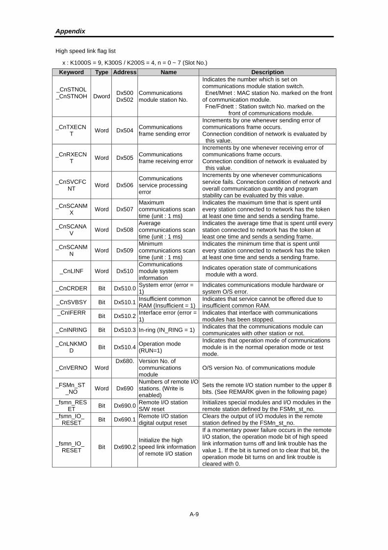
Appendix
A-9
High speed link flag list
x : K1000S = 9, K300S / K200S = 4, n = 0 ~ 7 (Slot No.)
Keyword Type Address Name Description
_CnSTNOL_CnSTNOH Dword
Dx500Dx502
Communicationsmodule station No.
Indicates the number which is set oncommunications module station switch. Enet/Mnet : MAC station No. marked on the frontof communication module. Fne/Fdnett : Station switch No. marked on the
front of communications module.
_CnTXECNT
Word Dx504Communicationsframe sending error
Increments by one whenever sending error ofcommunications frame occurs.Connection condition of network is evaluated by
this value.
_CnRXECNT
Word Dx505Communicationsframe receiving error
Increments by one whenever receiving error ofcommunications frame occurs.Connection condition of network is evaluated by
this value.
_CnSVCFCNT
Word Dx506Communicationsservice processingerror
Increments by one whenever communicationsservice fails. Connection condition of network andoverall communication quantity and programstability can be evaluated by this value.
_CnSCANMX
Word Dx507Maximumcommunications scantime (unit : 1 ms)
Indicates the maximum time that is spent untilevery station connected to network has the tokenat least one time and sends a sending frame.
_CnSCANAV
Word Dx508Averagecommunications scantime (unit : 1 ms)
Indicates the average time that is spent until everystation connected to network has the token atleast one time and sends a sending frame.
_CnSCANMN
Word Dx509Minimumcommunications scantime (unit : 1 ms)
Indicates the minimum time that is spent untilevery station connected to network has the tokenat least one time and sends a sending frame.
_CnLINF Word Dx510Communicationsmodule systeminformation
Indicates operation state of communicationsmodule with a word.
_CnCRDER Bit Dx510.0System error (error =1)
Indicates communications module hardware orsystem O/S error.
_CnSVBSY Bit Dx510.1Insufficient commonRAM (Insufficient = 1)
Indicates that service cannot be offered due toinsufficient common RAM.
_CnIFERRBit Dx510.2
Interface error (error =1)
Indicates that interface with communicationsmodules has been stopped.
_CnINRING Bit Dx510.3 In-ring (IN_RING = 1)Indicates that the communications module cancommunicates with other station or not.
_CnLNKMOD
Bit Dx510.4Operation mode(RUN=1)
Indicates that operation mode of communicationsmodule is in the normal operation mode or testmode.
_CnVERNO WordDx680. Version No. of
communicationsmodule
O/S version No. of communications module
_FSMn_ST_NO
Word Dx690Numbers of remote I/Ostations. (Write isenabled)
Sets the remote I/O station number to the upper 8bits. (See REMARK given in the following page)
_fsmn_RESET
Bit Dx690.0Remote I/O stationS/W reset
Initializes special modules and I/O modules in theremote station defined by the FSMn_st_no.
_fsmn_IO_RESET
Bit Dx690.1Remote I/O stationdigital output reset
Clears the output of I/O modules in the remotestation defined by the FSMn_st_no.
_fsmn_IO_RESET
Bit Dx690.2Initialize the highspeed link informationof remote I/O station
If a momentary power failure occurs in the remoteI/O station, the operation mode bit of high speedlink information turns off and link trouble has thevalue 1. If the bit is turned on to clear that bit, theoperation mode bit turns on and link trouble iscleared with 0.

Appendix
A-10
Slot No. & Flag List
Slot No. D area address Remark
1 Dx511 to Dx521
2 Dx522 to Dx532
3 Dx533 to Dx543
4 Dx544 to Dx554
5 Dx555 to Dx565
6 Dx566 to Dx576
7 Dx577 to Dx587
The address of the flag which is loaded onto the slot n iscalculated as shown below.
∗ Address of D area = Address shown in the [TABLE1] + 11 × n, where n = 1 to 7
Example) Address for the average communications scan timeof the communications module loaded on the slot 6.
→ Dx508 + 11 × 6 = Dx574
Detailed High Speed Link Information Flag List (when m=0)
KeywordTyp
e
BitAddres
sName Description
_HSmRLINK BitDx600.
0
High speed linknormal runinformation(RUN_LINK)
Indicates that all stations are normally operatingcomplying with the parameter set in the highspeed link. This flag turns on under the followingconditions.
1. All stations set in the parameter are in theRUN mode and have no error, and
2. All blocks set in the parameter normallycommunicate, and
3. The parameters set in all stations, which areset in the parameter, normally communicate.
Once this flag is turned on, it maintains thatstate as long as link disable does not make thatstate stopped.
_HSmLTRBL
BitDx600.
1
High speed linktrouble abnormal runinformation
This flag turns on when, under the condition that_HSmRLINK is turned on, communications ofthe stations and data blocks set in theparameter is under the following conditions.
1. A station set in the parameter is not in theRUN mode, or
2. A station set in the parameter has an error,or
3. The communications of data blocks set inthe parameter does not normally operate.
This flag turns on if the above conditions 1), 2)and 3) occur. If normal conditions are restored, itwill turn off again.
_HSmSTATE[k]
(k = 0 to 63)
BitArra
y
Dx601.0 to
Dx604.15
Overallcommunications stateinformation of K DataBlock set by the highlink parameter
Indicates overall communications state of everyblocks of the parameters set. _HSmSTATE[k] = _HSmMOD[k] &_HSmTRX[k] & _HSmERR[k]
_HSmMOD[k]
(k = 0 to 63)
BitArra
y
Dx605.0 to
Dx608.15
K Data Block settingstations modeinformation. (RUN =1, others =-0)
Indicates the operation modes of stations setthe K data block of parameters.
_HSmTRX[k]
(k = 0 to 63)
BitArra
y
Dx609.0 to
Dx612.15
K Data Blockcommunications stateinformation (Normal =1, abnormal = 0)
Indicates whether communications of the K datablock of parameters are normally operating asset .
_HSmERR[k]
(k = 0 to 63)
BitArra
y
Dx613.0 to
Dx616.15
K Data Block settingstations stateinformation. (Normal= 1, abnormal = 0)
Indicates whether the stations set in the K datablock of parameters have an error.
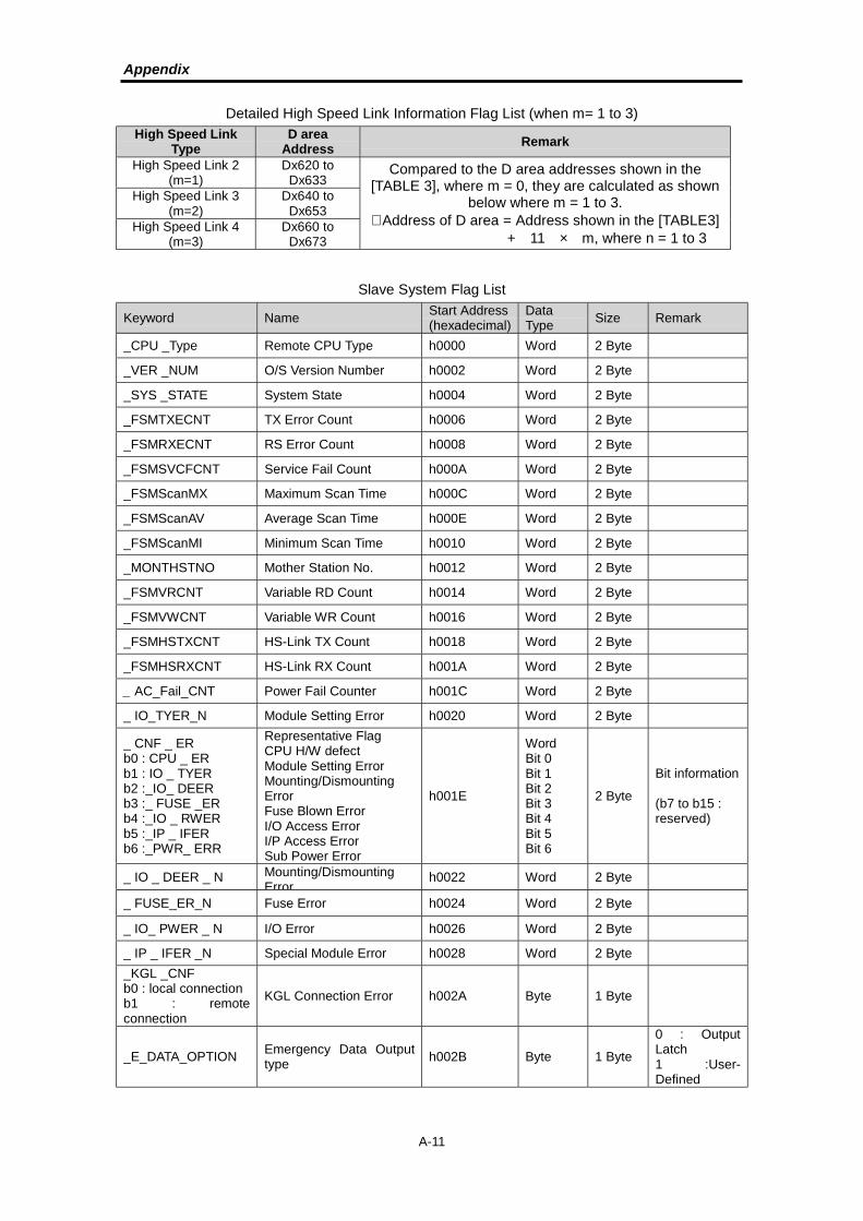
Appendix
A-11
Detailed High Speed Link Information Flag List (when m= 1 to 3)
High Speed LinkType
D areaAddress
Remark
High Speed Link 2(m=1)
Dx620 toDx633
High Speed Link 3(m=2)
Dx640 toDx653
High Speed Link 4(m=3)
Dx660 toDx673
Compared to the D area addresses shown in the[TABLE 3], where m = 0, they are calculated as shown
below where m = 1 to 3.∗ Address of D area = Address shown in the [TABLE3]
+ 11 × m, where n = 1 to 3
Slave System Flag List
Keyword NameStart Address(hexadecimal)
DataType
Size Remark
_CPU _Type Remote CPU Type h0000 Word 2 Byte
_VER _NUM O/S Version Number h0002 Word 2 Byte
_SYS _STATE System State h0004 Word 2 Byte
_FSMTXECNT TX Error Count h0006 Word 2 Byte
_FSMRXECNT RS Error Count h0008 Word 2 Byte
_FSMSVCFCNT Service Fail Count h000A Word 2 Byte
_FSMScanMX Maximum Scan Time h000C Word 2 Byte
_FSMScanAV Average Scan Time h000E Word 2 Byte
_FSMScanMI Minimum Scan Time h0010 Word 2 Byte
_MONTHSTNO Mother Station No. h0012 Word 2 Byte
_FSMVRCNT Variable RD Count h0014 Word 2 Byte
_FSMVWCNT Variable WR Count h0016 Word 2 Byte
_FSMHSTXCNT HS-Link TX Count h0018 Word 2 Byte
_FSMHSRXCNT HS-Link RX Count h001A Word 2 Byte
_ AC_Fail_CNT Power Fail Counter h001C Word 2 Byte
_ IO_TYER_N Module Setting Error h0020 Word 2 Byte
_ CNF _ ERb0 : CPU _ ERb1 : IO _ TYERb2 :_IO_ DEERb3 :_ FUSE _ERb4 :_IO _ RWERb5 :_IP _ IFERb6 :_PWR_ ERR
Representative FlagCPU H/W defectModule Setting ErrorMounting/DismountingErrorFuse Blown ErrorI/O Access ErrorI/P Access ErrorSub Power Error
h001E
WordBit 0Bit 1Bit 2Bit 3Bit 4Bit 5Bit 6
2 Byte
Bit information (b7 to b15 :reserved)
_ IO _ DEER _ N Mounting/DismountingError
h0022 Word 2 Byte
_ FUSE_ER_N Fuse Error h0024 Word 2 Byte
_ IO_ PWER _ N I/O Error h0026 Word 2 Byte
_ IP _ IFER _N Special Module Error h0028 Word 2 Byte
_KGL _CNFb0 : local connectionb1 : remoteconnection
KGL Connection Error h002A Byte 1 Byte
_E_DATA_OPTIONEmergency Data Outputtype
h002B Byte 1 Byte
0 : OutputLatch1 :User-Defined
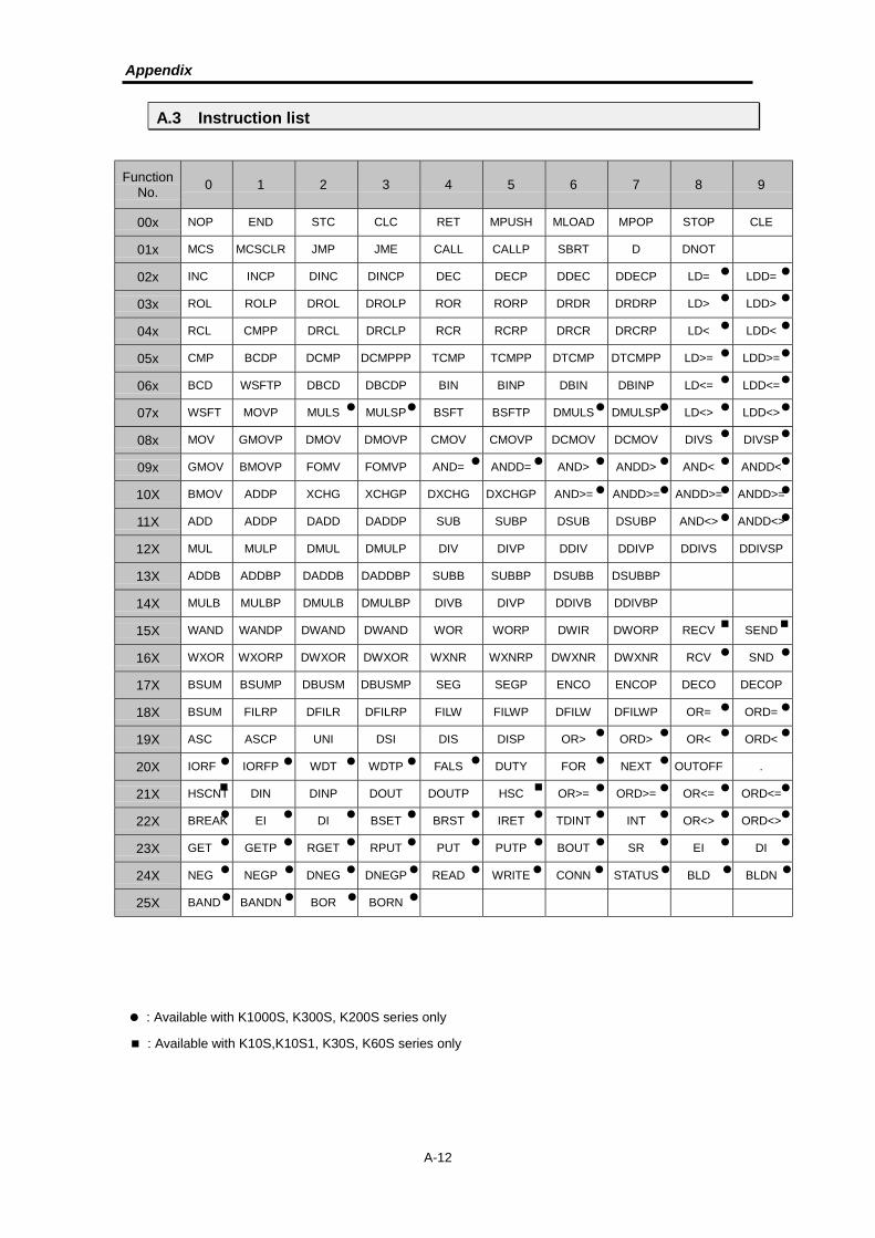
Appendix
A-12
A.3 Instruction list
FunctionNo.
0 1 2 3 4 5 6 7 8 9
00x NOP END STC CLC RET MPUSH MLOAD MPOP STOP CLE
01x MCS MCSCLR JMP JME CALL CALLP SBRT D DNOT
02x INC INCP DINC DINCP DEC DECP DDEC DDECP LD= LDD=
03x ROL ROLP DROL DROLP ROR RORP DRDR DRDRP LD> LDD>
04x RCL CMPP DRCL DRCLP RCR RCRP DRCR DRCRP LD< LDD<
05x CMP BCDP DCMP DCMPPP TCMP TCMPP DTCMP DTCMPP LD>= LDD>=
06x BCD WSFTP DBCD DBCDP BIN BINP DBIN DBINP LD<= LDD<=
07x WSFT MOVP MULS MULSP BSFT BSFTP DMULS DMULSP LD<> LDD<>
08x MOV GMOVP DMOV DMOVP CMOV CMOVP DCMOV DCMOV DIVS DIVSP
09x GMOV BMOVP FOMV FOMVP AND= ANDD= AND> ANDD> AND< ANDD<
10X BMOV ADDP XCHG XCHGP DXCHG DXCHGP AND>= ANDD>= ANDD>= ANDD>=
11X ADD ADDP DADD DADDP SUB SUBP DSUB DSUBP AND<> ANDD<>
12X MUL MULP DMUL DMULP DIV DIVP DDIV DDIVP DDIVS DDIVSP
13X ADDB ADDBP DADDB DADDBP SUBB SUBBP DSUBB DSUBBP
14X MULB MULBP DMULB DMULBP DIVB DIVP DDIVB DDIVBP
15X WAND WANDP DWAND DWAND WOR WORP DWIR DWORP RECV SEND
16X WXOR WXORP DWXOR DWXOR WXNR WXNRP DWXNR DWXNR RCV SND
17X BSUM BSUMP DBUSM DBUSMP SEG SEGP ENCO ENCOP DECO DECOP
18X BSUM FILRP DFILR DFILRP FILW FILWP DFILW DFILWP OR= ORD=
19X ASC ASCP UNI DSI DIS DISP OR> ORD> OR< ORD<
20X IORF IORFP WDT WDTP FALS DUTY FOR NEXT OUTOFF .
21X HSCNT DIN DINP DOUT DOUTP HSC OR>= ORD>= OR<= ORD<=
22X BREAK EI DI BSET BRST IRET TDINT INT OR<> ORD<>
23X GET GETP RGET RPUT PUT PUTP BOUT SR EI DI
24X NEG NEGP DNEG DNEGP READ WRITE CONN STATUS BLD BLDN
25X BAND BANDN BOR BORN
"
! : Available with K1000S, K300S, K200S series only
: Available with K10S,K10S1, K30S, K60S series only
"
!! ! !
!!!!!!!!!!
! ! ! ! ! ! ! ! ! !
! ! ! ! ! ! ! ! ! !
! ! ! !
! !!! ! ! !
! ! ! !
! !
! !
! ! ! ! ! !
! !
! !
! ! ! ! ! !
! ! ! !
! !
! !
! !
! !
! !
"
" "