Embed Size (px)
Citation preview
Smart Measurement Solutions®
Bode 100 - Application Note
Input Impedance Measurements
for Stable Input-Filter Design
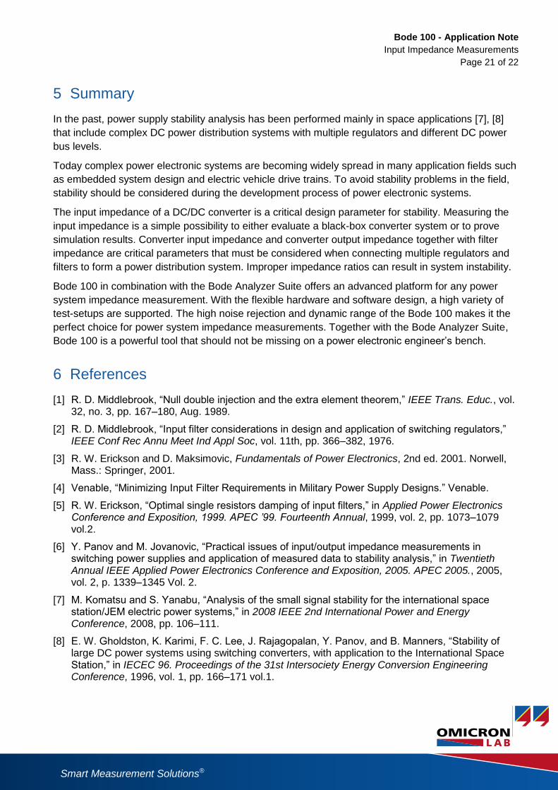
0,01
0,1
1
10
100
1000
10 100 1000 10000 100000
Converter Input Impedance
Filter Output Impedance
By Florian Hämmerle
© 2017 by OMICRON Lab – V1.0
Visit www.omicron-lab.com for more information.
Contact [email protected] for technical support.
Bode 100 - Application Note
Input Impedance Measurements
Page 2 of 22
Smart Measurement Solutions
Smart Measurement Solutions®
Table of Contents
1 Executive Summary .................................................................................................................... 3
2 The Input Filter Can Degrade System Stability ......................................................................... 3
2.1 Middlebrook’s Extra-Element Theorem ....................................................................................... 3
2.2 Reducing the Influence of the Input Filter ................................................................................... 4
2.3 Simplified Black-Box Stability Criterion ....................................................................................... 4
2.4 Negative Resistance Causes Oscillation .................................................................................... 5
3 Experimental Verification ........................................................................................................... 6
3.1 DC/DC Converter Under Test ..................................................................................................... 6
3.2 Adding an Input Filter to Reduce Input Current Ripple ................................................................ 7
3.3 Influence on the Stability of the Converter .................................................................................. 8
3.4 Influence on the Transient Response ......................................................................................... 9
3.5 Impedance Ratio ........................................................................................................................ 9
3.6 Damping the Input Filter ........................................................................................................... 10
4 Measuring the Input Impedance of a DC/DC Converter ......................................................... 12
4.1 Voltage / Current Method .......................................................................................................... 12
4.2 Voltage/Current Measurement Mode ........................................................................................ 13
4.3 Modulating the DC Input Signal ................................................................................................ 14
4.3.1 J2120A Line Injector from Picotest ..................................................................................... 14
4.3.2 Configurable Power Amplifier ............................................................................................. 15
4.3.3 Capacitive or Inductive Injection ......................................................................................... 15
4.4 Measuring the AC Voltage ........................................................................................................ 17
4.5 Measuring the AC Current ........................................................................................................ 18
4.6 Calibrating the Test Setup ........................................................................................................ 19
4.6.1 Thru Calibration ................................................................................................................. 19
4.6.2 Open/Short/Load Calibration .............................................................................................. 20
4.7 Measurement Setup Verification ............................................................................................... 20
5 Summary ................................................................................................................................... 21
6 References ................................................................................................................................ 21
Note: Basic procedures such as setting-up, adjusting and calibrating the Bode 100 are described in
the Bode 100 user manual. You can download the Bode 100 user manual at www.omicron-
lab.com/bode-100/downloads#3
Note: All measurements in this application note have been performed with the Bode Analyzer Suite
V3.11 Use this version or a higher version to perform the measurements shown in this
document. You can download the latest version at
www.omicron-lab.com/bode-100/downloads
Bode 100 - Application Note
Input Impedance Measurements
Page 3 of 22
Smart Measurement Solutions
Smart Measurement Solutions®
1 Executive Summary
This application note describes why the input impedance of a DC/DC power converter is an essential
parameter for a stable system design. The theory of the filter stability problem is reviewed in
section 2. To show that input filter instability is not only a theoretical problem but can also happen in
real live, an experiment with a bad input filter design and its effect on system stability are
demonstrated in section 3. Finally, different possible input impedance measurement setups are
presented and discussed in section 4.
2 The Input Filter Can Degrade System Stability
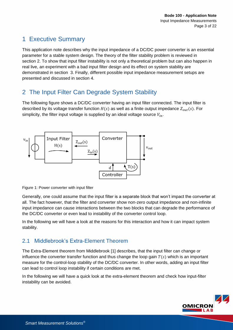
The following figure shows a DC/DC converter having an input filter connected. The input filter is
described by its voltage transfer function 𝐻(𝑠) as well as a finite output impedance 𝑍𝑜𝑢𝑡(𝑠). For
simplicity, the filter input voltage is supplied by an ideal voltage source 𝑉𝑖𝑛.
Figure 1: Power converter with input filter
Generally, one could assume that the input filter is a separate block that won’t impact the converter at
all. The fact however, that the filter and converter show non-zero output impedance and non-infinite
input impedance can cause interactions between the two blocks that can degrade the performance of
the DC/DC converter or even lead to instability of the converter control loop.
In the following we will have a look at the reasons for this interaction and how it can impact system
stability.
2.1 Middlebrook’s Extra-Element Theorem
The Extra-Element theorem from Middlebrook [1] describes, that the input filter can change or
influence the converter transfer function and thus change the loop gain 𝑇(𝑠) which is an important
measure for the control-loop stability of the DC/DC converter. In other words, adding an input filter
can lead to control loop instability if certain conditions are met.
In the following we will have a quick look at the extra-element theorem and check how input-filter
instability can be avoided.
Bode 100 - Application Note
Input Impedance Measurements
Page 4 of 22
Smart Measurement Solutions
Smart Measurement Solutions®
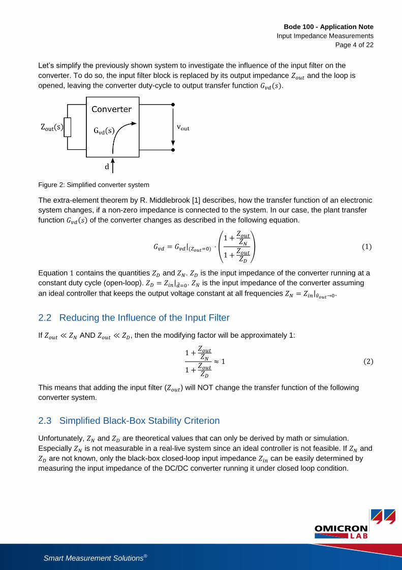
Let’s simplify the previously shown system to investigate the influence of the input filter on the
converter. To do so, the input filter block is replaced by its output impedance 𝑍𝑜𝑢𝑡 and the loop is
opened, leaving the converter duty-cycle to output transfer function 𝐺𝑣𝑑(𝑠).
Figure 2: Simplified converter system
The extra-element theorem by R. Middlebrook [1] describes, how the transfer function of an electronic
system changes, if a non-zero impedance is connected to the system. In our case, the plant transfer
function 𝐺𝑣𝑑(𝑠) of the converter changes as described in the following equation.
𝐺𝑣𝑑 = 𝐺𝑣𝑑|(𝑍𝑜𝑢𝑡=0) ⋅ (1 +
𝑍𝑜𝑢𝑡𝑍𝑁
1 +𝑍𝑜𝑢𝑡𝑍𝐷
) (1)
Equation 1 contains the quantities 𝑍𝐷 and 𝑍𝑁. 𝑍𝐷 is the input impedance of the converter running at a
constant duty cycle (open-loop). 𝑍𝐷 = 𝑍𝑖𝑛|�̂�=0. 𝑍𝑁 is the input impedance of the converter assuming
an ideal controller that keeps the output voltage constant at all frequencies 𝑍𝑁 = 𝑍𝑖𝑛|�̂�𝑜𝑢𝑡→0.
2.2 Reducing the Influence of the Input Filter
If 𝑍𝑜𝑢𝑡 ≪ 𝑍𝑁 AND 𝑍𝑜𝑢𝑡 ≪ 𝑍𝐷, then the modifying factor will be approximately 1:
1 +𝑍𝑜𝑢𝑡𝑍𝑁
1 +𝑍𝑜𝑢𝑡𝑍𝐷
≈ 1 (2)
This means that adding the input filter (𝑍𝑜𝑢𝑡) will NOT change the transfer function of the following
converter system.
2.3 Simplified Black-Box Stability Criterion
Unfortunately, 𝑍𝑁 and 𝑍𝐷 are theoretical values that can only be derived by math or simulation.
Especially 𝑍𝑁 is not measurable in a real-live system since an ideal controller is not feasible. If 𝑍𝑁 and
𝑍𝐷 are not known, only the black-box closed-loop input impedance 𝑍𝑖𝑛 can be easily determined by
measuring the input impedance of the DC/DC converter running it under closed loop condition.
Bode 100 - Application Note
Input Impedance Measurements
Page 5 of 22
Smart Measurement Solutions
Smart Measurement Solutions®
According to [2, Sec. 5.3] the following simplified condition is sufficient to prove system stability. In
words; for guaranteed system stability, the output impedance of the input filter must be much smaller
than the input impedance of the closed-loop converter.
|𝑍𝑜𝑢𝑡| ≪ |𝑍𝑖𝑛| (3)
If the phase information is available, even the full Nyquist stability criterion can be applied to the
following ratio.
𝑇 =
𝑍𝑜𝑢𝑡
𝑍𝑖𝑛
(4)
The closed-loop input impedance 𝑍𝑖𝑛 is not sufficient to prove that the input filter won’t have an impact
on the transfer function of the converter but it is sufficient to check for system stability.
In other words; by measuring converter input impedance and filter output impedance one can prove
system stability but cannot conclude that the input filter won’t change the system dynamic behavior.
2.4 Negative Resistance Causes Oscillation
The control loop of a converter keeps the output voltage 𝑉𝑜𝑢𝑡 constant. Assuming a constant load
𝑅𝑙𝑜𝑎𝑑 at the converter output, the output current 𝐼𝑜𝑢𝑡 will also stay constant.
Constant output voltage and constant output current lead to constant output power 𝑃𝑜𝑢𝑡. If we assume
that the converter has 100% efficiency, input power equals output power 𝑃𝑖𝑛 = 𝑃𝑜𝑢𝑡.
Now let’s assume the input voltage of the converter 𝑉𝑖𝑛 increases by 10%. The converter regulation
will keep the output voltage and therefore output power constant. The input power must stay constant
as well since the converter cannot dissipate any power. To achieve this, the input current 𝐼𝑖𝑛 must
now decrease by 10%.
The fact that increasing the voltage causes the current to drop can be described as a negative
resistance. A positive resistance would cause the current to rise if the voltage rises (𝑅 = 𝑉/𝐼).
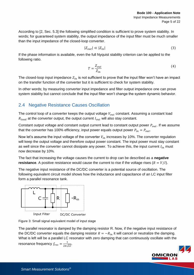
The negative input resistance of the DC/DC converter is a potential source of oscillation. The
following equivalent circuit model shows how the inductance and capacitance of an LC input filter
form a parallel resonance tank.
Figure 3: Small signal equivalent model of input stage
The parallel resonator is damped by the damping resistor R. Now, if the negative input resistance of
the DC/DC converter equals the damping resistor 𝑅 = −𝑅𝑖𝑛 it will cancel or neutralize the damping.
What is left will be a parallel LC resonator with zero damping that can continuously oscillate with the
resonance frequency 𝑓𝑟𝑒𝑠 =1
2𝜋√𝐿𝐶.
Bode 100 - Application Note
Input Impedance Measurements
Page 6 of 22
Smart Measurement Solutions
Smart Measurement Solutions®
3 Experimental Verification
The input filter stability problem is well known in theory but does it really happen in a real live
application?
The fact that the loop bandwidth is generally limited helps to avoid negative resistance oscillation.
Negative resistance only appears at frequencies where the loop gain of the converter is sufficiently
high and the converter shows good regulation. Depending on the speed of the control loop this
frequency can be between hundreds of Hz up to decades of kHz.
The negative resistance oscillation occurs if the resonance frequency of the input filter falls into the
negative resistance region of the converter. This means that the resonance frequency of the filter
must be well below the crossover frequency of the converter. This generally only happens if either the
control loop is very fast or the input filter is rather big.
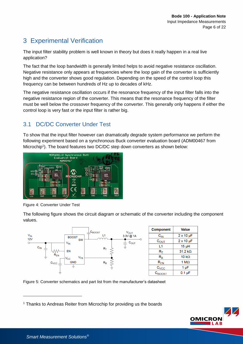
3.1 DC/DC Converter Under Test
To show that the input filter however can dramatically degrade system performance we perform the
following experiment based on a synchronous Buck converter evaluation board (ADM00467 from
Microchip1). The board features two DC/DC step down converters as shown below:
Figure 4: Converter Under Test
The following figure shows the circuit diagram or schematic of the converter including the component
values.
Figure 5: Converter schematics and part list from the manufacturer’s datasheet
1 Thanks to Andreas Reiter from Microchip for providing us the boards
Bode 100 - Application Note
Input Impedance Measurements
Page 7 of 22
Smart Measurement Solutions
Smart Measurement Solutions®
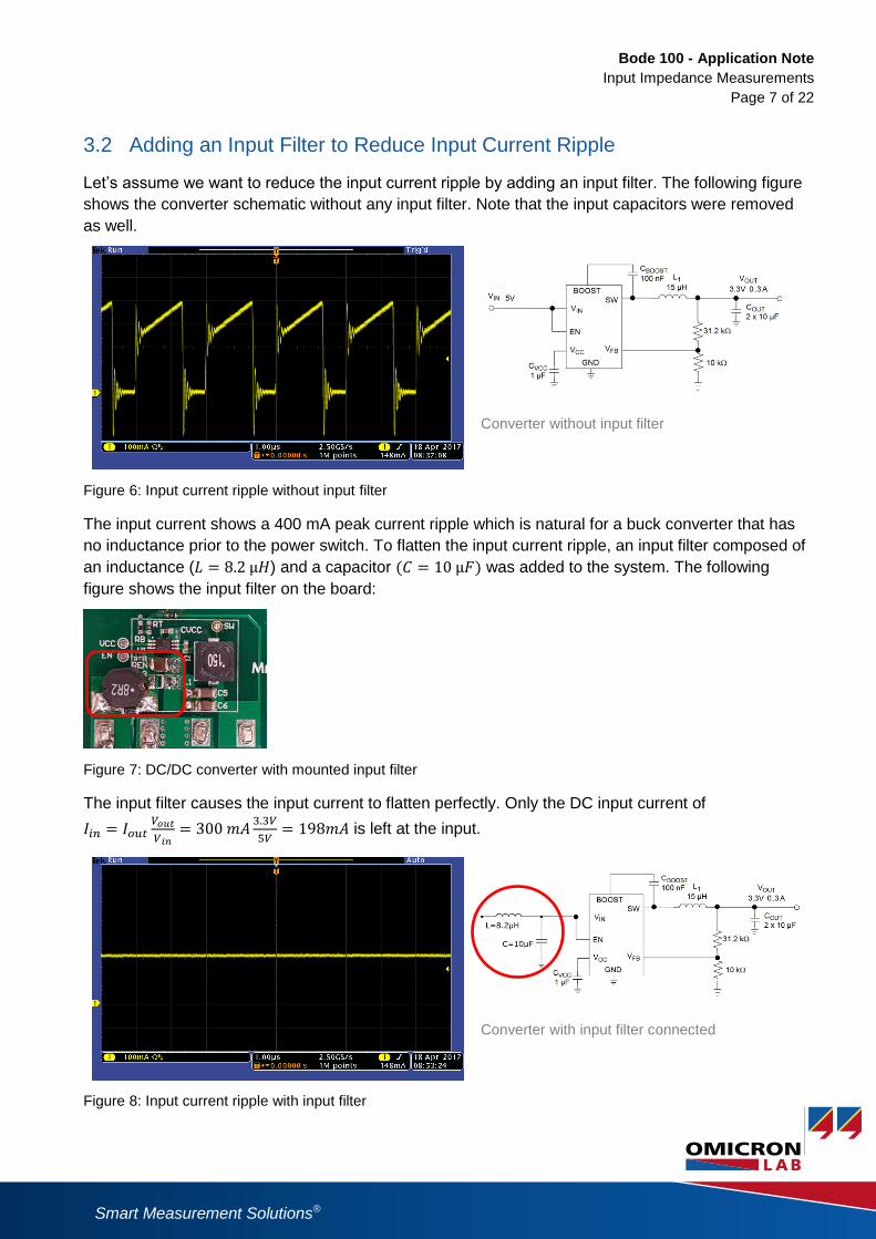
3.2 Adding an Input Filter to Reduce Input Current Ripple
Let’s assume we want to reduce the input current ripple by adding an input filter. The following figure
shows the converter schematic without any input filter. Note that the input capacitors were removed
as well.
Converter without input filter
Figure 6: Input current ripple without input filter
The input current shows a 400 mA peak current ripple which is natural for a buck converter that has
no inductance prior to the power switch. To flatten the input current ripple, an input filter composed of
an inductance (𝐿 = 8.2 µ𝐻) and a capacitor (𝐶 = 10 µ𝐹) was added to the system. The following
figure shows the input filter on the board:
Figure 7: DC/DC converter with mounted input filter
The input filter causes the input current to flatten perfectly. Only the DC input current of
𝐼𝑖𝑛 = 𝐼𝑜𝑢𝑡𝑉𝑜𝑢𝑡
𝑉𝑖𝑛= 300 𝑚𝐴
3.3𝑉
5𝑉= 198𝑚𝐴 is left at the input.
Converter with input filter connected
Figure 8: Input current ripple with input filter
Bode 100 - Application Note
Input Impedance Measurements
Page 8 of 22
Smart Measurement Solutions
Smart Measurement Solutions®
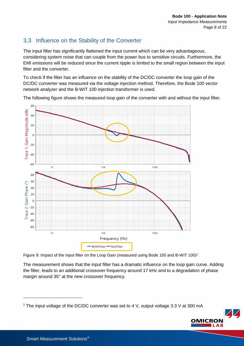
3.3 Influence on the Stability of the Converter
The input filter has significantly flattened the input current which can be very advantageous,
considering system noise that can couple from the power bus to sensitive circuits. Furthermore, the
EMI emissions will be reduced since the current ripple is limited to the small region between the input
filter and the converter.
To check if the filter has an influence on the stability of the DC/DC converter the loop gain of the
DC/DC converter was measured via the voltage injection method. Therefore, the Bode 100 vector
network analyzer and the B-WIT 100 injection transformer is used.
The following figure shows the measured loop gain of the converter with and without the input filter.
Figure 9: Impact of the input filter on the Loop Gain (measured using Bode 100 and B-WIT 100)2
The measurement shows that the input filter has a dramatic influence on the loop gain curve. Adding
the filter, leads to an additional crossover frequency around 17 kHz and to a degradation of phase
margin around 35° at the new crossover frequency.
2 The input voltage of the DC/DC converter was set to 4 V, output voltage 3.3 V at 300 mA
Bode 100 - Application Note
Input Impedance Measurements
Page 9 of 22
Smart Measurement Solutions
Smart Measurement Solutions®
3.4 Influence on the Transient Response
To check how the degraded loop gain impacts the transient response a small-signal load step test
was performed. 50 mA load steps were generated using a Picotest J2111A current injector and a
Picotest G5100A arbitrary waveform generator. The following figure shows the transient response
without input filter on the left-hand side and the transient response with input filter on the right-hand
side.
Figure 10: Impact of the input filter on the transient response3
The transient response with input filter shows clearly degraded performance. Excessive ringing at
approximately 17 kHz appears after each load step. This ringing is not present without the input filter.
Note that the ringing is undesired and can significantly degrade performance when powering a
sensitive circuit.
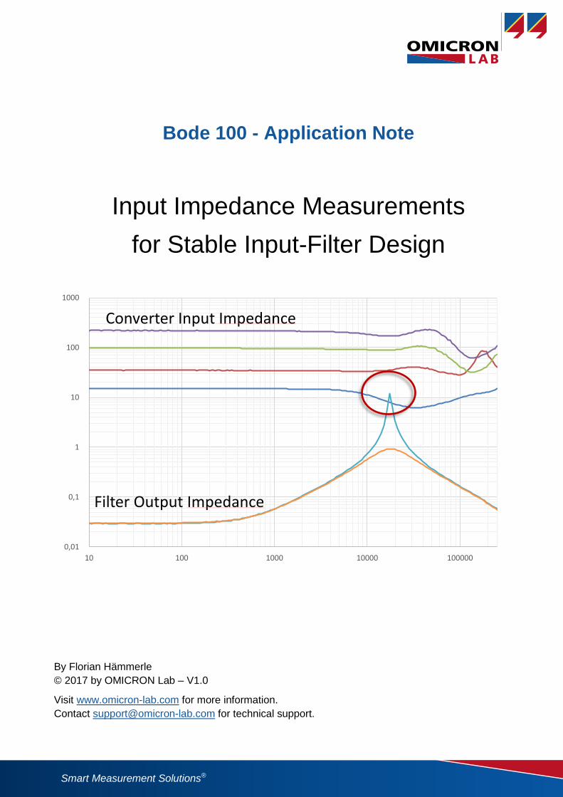
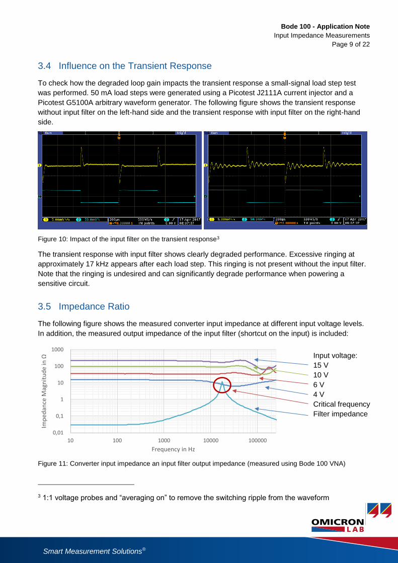
3.5 Impedance Ratio
The following figure shows the measured converter input impedance at different input voltage levels.
In addition, the measured output impedance of the input filter (shortcut on the input) is included:
Figure 11: Converter input impedance an input filter output impedance (measured using Bode 100 VNA)
3 1:1 voltage probes and “averaging on” to remove the switching ripple from the waveform
0,01
0,1
1
10
100
1000
10 100 1000 10000 100000
Imp
edan
ce M
agn
itu
de
in Ω
Frequency in Hz
Input voltage:
15 V
10 V
6 V
4 V
Critical frequency
Filter impedance
Bode 100 - Application Note
Input Impedance Measurements
Page 10 of 22
Smart Measurement Solutions
Smart Measurement Solutions®
Figure 11 clearly shows that the measured closed-loop input impedance of the converter and the
output impedance of the filter intersect at ≈ 17 𝑘𝐻𝑧. The input filter impedance at resonance peaks
above 10 Ω, whereas the converter input impedance is below 10 Ω at an input voltage of 4 V. The
impedance peak of the input filter resonance is clearly the reason for the system oscillation at 17 kHz.
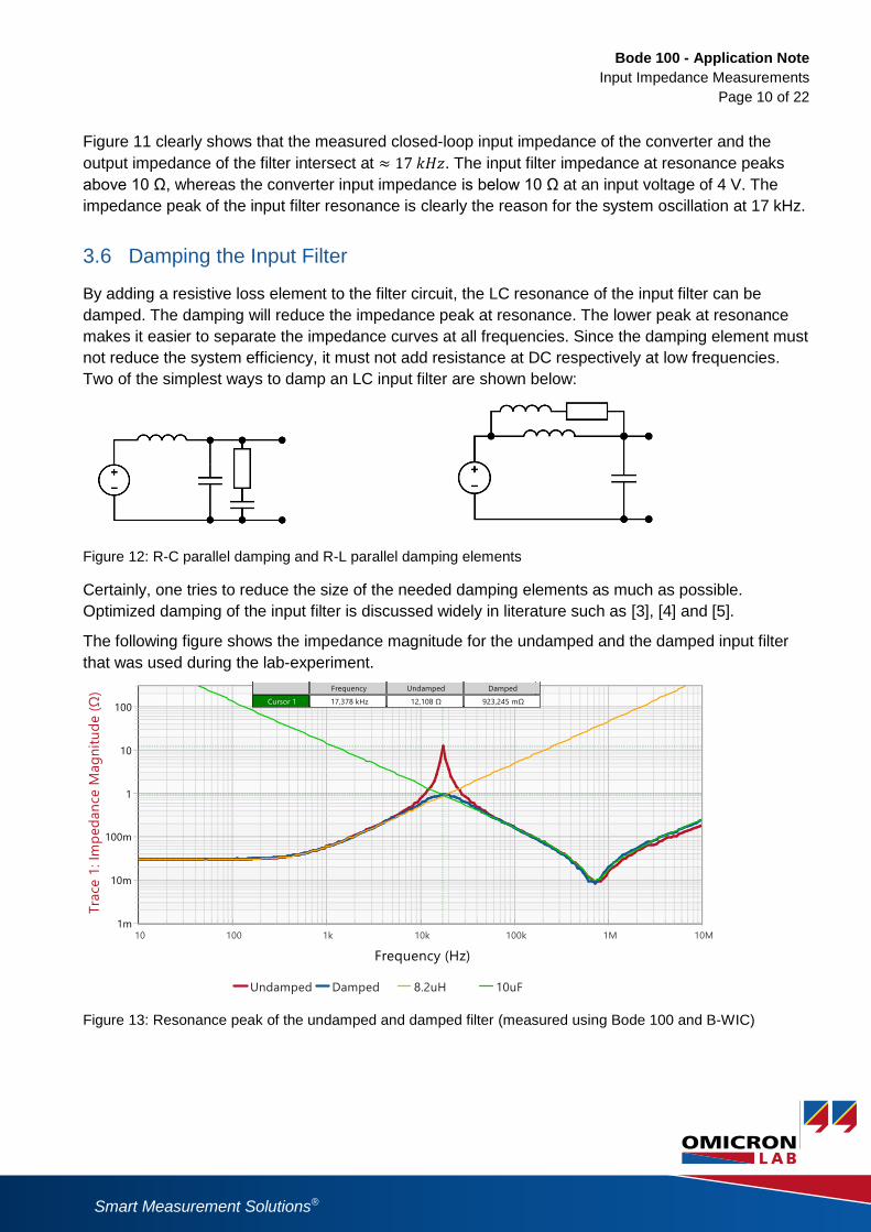
3.6 Damping the Input Filter
By adding a resistive loss element to the filter circuit, the LC resonance of the input filter can be
damped. The damping will reduce the impedance peak at resonance. The lower peak at resonance
makes it easier to separate the impedance curves at all frequencies. Since the damping element must
not reduce the system efficiency, it must not add resistance at DC respectively at low frequencies.
Two of the simplest ways to damp an LC input filter are shown below:
Figure 12: R-C parallel damping and R-L parallel damping elements
Certainly, one tries to reduce the size of the needed damping elements as much as possible.
Optimized damping of the input filter is discussed widely in literature such as [3], [4] and [5].
The following figure shows the impedance magnitude for the undamped and the damped input filter
that was used during the lab-experiment.
Figure 13: Resonance peak of the undamped and damped filter (measured using Bode 100 and B-WIC)

Bode 100 - Application Note
Input Impedance Measurements
Page 11 of 22
Smart Measurement Solutions
Smart Measurement Solutions®
Figure 13 shows that the impedance peak was lowered from ≈12 Ω to ≈1 Ω by adding a damping
element to the filter. The impact on the loop gain of the converter was also lowered as shown in the
following figure:
Figure 14: Damping the input filter reduces impact on loop gain
The loop gain does show that the second crossover frequency that was added by the input filter
disappears when the input filter is damped. The damping also recuperates the transient response as
shown in the following figure.
Figure 15: Improving transient response by damping the input filter
Filter damping

Bode 100 - Application Note
Input Impedance Measurements
Page 12 of 22
Smart Measurement Solutions
Smart Measurement Solutions®
4 Measuring the Input Impedance of a DC/DC Converter
The AC input impedance of a DC/DC converter can be measured using various methods. The input
impedance measurement of a 100 mW converter will require a completely different test-setup than the
input impedance measurement of a 100 kW converter. The basic measurement concept however
generally stays the same for all power levels. In the following the Voltage/Current method is explained
in detail.
4.1 Voltage / Current Method
The input impedance is defined as the quotient of AC input voltage and AC input current.
𝑍𝑖𝑛 =
𝑣𝑖𝑛
𝑖�̂�𝑛
(5)
To be able to measure the input impedance an AC disturbance must be added to the DC supply
voltage. Then the input impedance can be evaluated by comparing the size of voltage ripple and
corresponding current ripple as shown in equation 5.
The following figure shows the basic test setup that can be used to measure the input impedance of
the DC/DC converter (DUT4) using the Bode 100 vector network analyzer / frequency response
analyzer.
Figure 16: Input impedance measurement setup (Using Bode 100 VNA)
By connecting the Bode 100 in this way and choosing the “Voltage/Current” impedance measurement
mode in the Bode Analyzer Suite software, the Bode 100 measures the input impedance of the DUT
by performing the complex division 𝑍 =𝑉𝐶𝐻2
𝑉𝐶𝐻1. The used stepped sine-wave frequency response
measurement method offers the high sensitivity and noise-rejection needed to achieve high-dynamic-
range results on DUTs that generate a lot of switching noise.
4 Device Under Test
Bode 100 - Application Note
Input Impedance Measurements
Page 13 of 22
Smart Measurement Solutions
Smart Measurement Solutions®
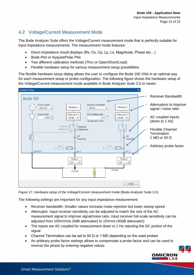
4.2 Voltage/Current Measurement Mode
The Bode Analyzer Suite offers the Voltage/Current measurement mode that is perfectly suitable for
input impedance measurements. The measurement mode features:
• Direct impedance result displays (Rs, Cs, Cp, Lp, Ls, Magnitude, Phase etc…)
• Bode-Plot or Nyquist/Polar Plot
• Two different calibration methods (Thru or Open/Short/Load)
• Flexible hardware setup for various measurement setup possibilities
The flexible hardware setup dialog allows the user to configure the Bode 100 VNA in an optimal way
for each measurement setup or probe-configuration. The following figure shows the hardware setup of
the Voltage/Current measurement mode available in Bode Analyzer Suite 3.0 or newer.
Figure 17: Hardware setup of the Voltage/Current measurement mode (Bode Analyzer Suite 3.X)
The following settings are important for any input impedance measurement:
• Receiver bandwidth: Smaller values increase noise-rejection but lower sweep speed
• Attenuator: Input receiver sensitivity can be adjusted to match the size of the AC
measurement signal to improve signal/noise ratio. Input receiver full-scale sensitivity can be
adjusted from 100mVrms (0dB attenuator) to 10Vrms (40dB attenuator)
• The inputs are AC coupled for measurement down to 1 Hz rejecting the DC portion of the
signal
• Channel Termination can be set to 50 Ω or 1 MΩ depending on the used probes
• An arbitrary probe factor settings allows to compensate a probe factor and can be used to
reverse the phase by entering negative values
• Receiver Bandwidth
• Attenuators to improve signal / noise ratio
• AC coupled inputs (down to 1 Hz)
• Flexible Channel Termination 1 MΩ or 50 Ω
• Arbitrary probe factor
Bode 100 - Application Note
Input Impedance Measurements
Page 14 of 22
Smart Measurement Solutions
Smart Measurement Solutions®
4.3 Modulating the DC Input Signal
Depending on the power level of your application, this is the trickiest part of the entire input
impedance measurement. The challenge is to modulate the DC supply proportionally to the Bode 100
output signal such that the AC signal is added to the DC supply. Depending on the voltage level and
power level of the DUT this can be quite easy or very challenging.
In the following we will have a closer look at the following measurement methods:
• Modulate the DC supply using a line injector such as the Picotest J2120A
• Modulate the DC supply line using a linear power amplifier featuring a DC offset
• Injecting to the DC supply via inductive coupling
• Injecting to the DC supply via capacitive coupling
Note that there are many more measurement methods possible as shown in e.g. [6].
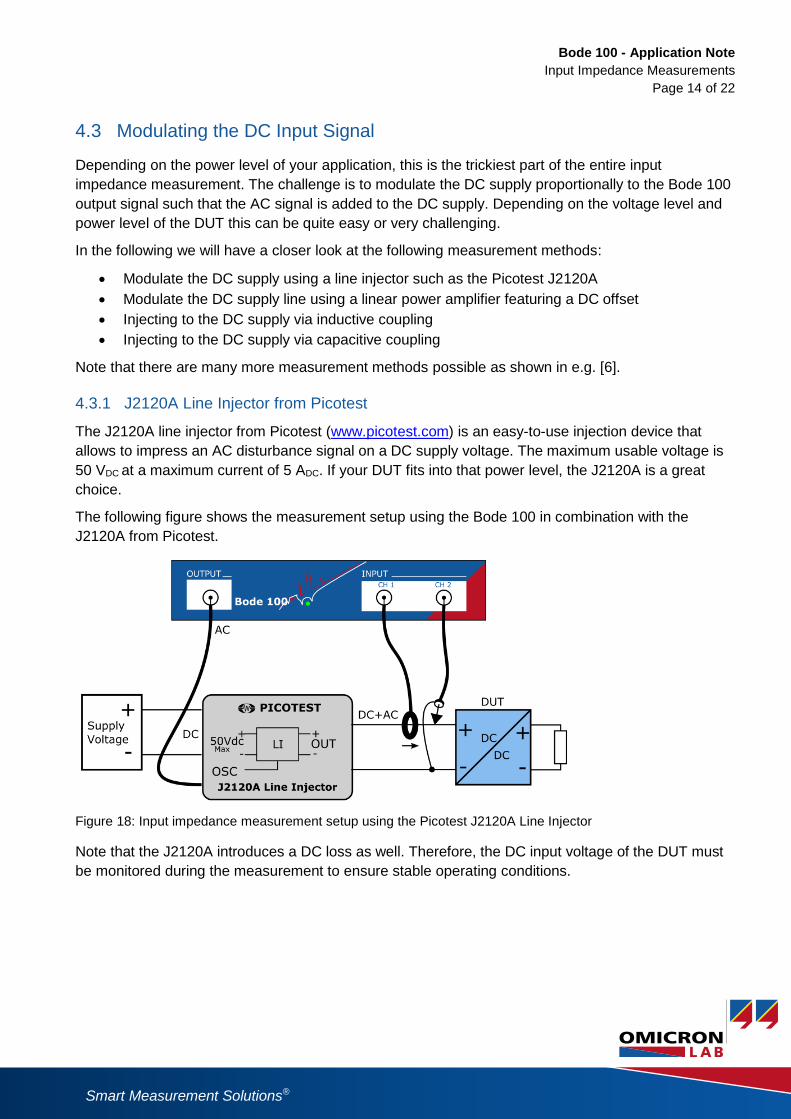
4.3.1 J2120A Line Injector from Picotest
The J2120A line injector from Picotest (www.picotest.com) is an easy-to-use injection device that
allows to impress an AC disturbance signal on a DC supply voltage. The maximum usable voltage is
50 VDC at a maximum current of 5 ADC. If your DUT fits into that power level, the J2120A is a great
choice.
The following figure shows the measurement setup using the Bode 100 in combination with the
J2120A from Picotest.
Figure 18: Input impedance measurement setup using the Picotest J2120A Line Injector
Note that the J2120A introduces a DC loss as well. Therefore, the DC input voltage of the DUT must
be monitored during the measurement to ensure stable operating conditions.
Bode 100 - Application Note
Input Impedance Measurements
Page 15 of 22
Smart Measurement Solutions
Smart Measurement Solutions®
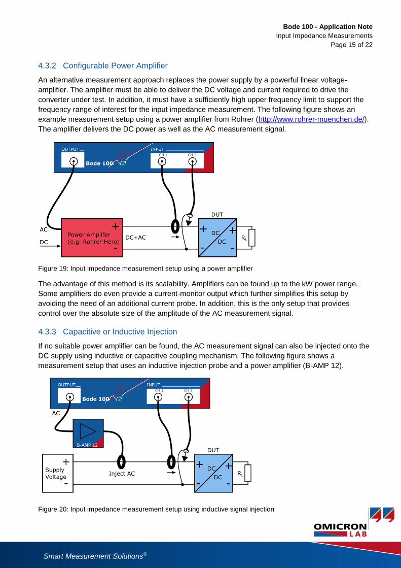
4.3.2 Configurable Power Amplifier
An alternative measurement approach replaces the power supply by a powerful linear voltage-
amplifier. The amplifier must be able to deliver the DC voltage and current required to drive the
converter under test. In addition, it must have a sufficiently high upper frequency limit to support the
frequency range of interest for the input impedance measurement. The following figure shows an
example measurement setup using a power amplifier from Rohrer (http://www.rohrer-muenchen.de/).
The amplifier delivers the DC power as well as the AC measurement signal.
Figure 19: Input impedance measurement setup using a power amplifier
The advantage of this method is its scalability. Amplifiers can be found up to the kW power range.
Some amplifiers do even provide a current-monitor output which further simplifies this setup by
avoiding the need of an additional current probe. In addition, this is the only setup that provides
control over the absolute size of the amplitude of the AC measurement signal.
4.3.3 Capacitive or Inductive Injection
If no suitable power amplifier can be found, the AC measurement signal can also be injected onto the
DC supply using inductive or capacitive coupling mechanism. The following figure shows a
measurement setup that uses an inductive injection probe and a power amplifier (B-AMP 12).
Figure 20: Input impedance measurement setup using inductive signal injection

Bode 100 - Application Note
Input Impedance Measurements
Page 16 of 22
Smart Measurement Solutions
Smart Measurement Solutions®
Alternatively, capacitive coupling can be used as well. The capacitor is used to block the DC voltage
from arriving at the injecting amplifier or measurement equipment as shown in the figure below.
Figure 21: Input impedance measurement setup using capacitive signal injection
The above-mentioned injection methods might require a higher power level than the +13 dBm
maximum power of the Bode 100. Therefore, the B-AMP 12 power amplifier was included in the
measurement setup. B-AMP 12 provides additional 12 dB of amplification resulting in a maximum
injecting power of 25 dBm (316 mW). Certainly, any third-party amplifier can be used to increase the
injection power even further.
The advantages of these injection methods is their full scalability. Depending on the choice of the
inductive or capacitive injection methods, nearly any power level can be measured. The inductive
injection offers further on the advantage of galvanic isolation. When suitable probes are used, a fully
isolated test system can be employed using inductive injection. Note that injection clamps or current
transformers needed for these measurements are hard to find or need to be custom-made.
Hint: It might be advantageous to provide a low-impedance path to the injected signal on the supply
side as shown in the following figure. This will improve the results especially at higher frequencies.
Figure 22: Providing a low-impedance path for the injected signal
Bode 100 - Application Note
Input Impedance Measurements
Page 17 of 22
Smart Measurement Solutions
Smart Measurement Solutions®
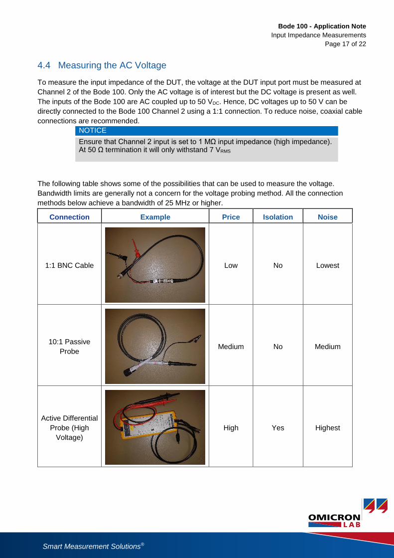
4.4 Measuring the AC Voltage
To measure the input impedance of the DUT, the voltage at the DUT input port must be measured at
Channel 2 of the Bode 100. Only the AC voltage is of interest but the DC voltage is present as well.
The inputs of the Bode 100 are AC coupled up to 50 VDC. Hence, DC voltages up to 50 V can be
directly connected to the Bode 100 Channel 2 using a 1:1 connection. To reduce noise, coaxial cable
connections are recommended.
NOTICE
Ensure that Channel 2 input is set to 1 MΩ input impedance (high impedance). At 50 Ω termination it will only withstand 7 VRMS
The following table shows some of the possibilities that can be used to measure the voltage.
Bandwidth limits are generally not a concern for the voltage probing method. All the connection
methods below achieve a bandwidth of 25 MHz or higher.
Connection Example Price Isolation Noise
1:1 BNC Cable
Low No Lowest
10:1 Passive
Probe
Medium No Medium
Active Differential
Probe (High
Voltage)
High Yes Highest
Bode 100 - Application Note
Input Impedance Measurements
Page 18 of 22
Smart Measurement Solutions
Smart Measurement Solutions®
NOTICE
Do not apply more than 50 VDC to the input channels of Bode 100! Even a passive 10:1 probe with 10 MΩ input impedance cannot be used to increase the DC capability since the inputs are AC-coupled!
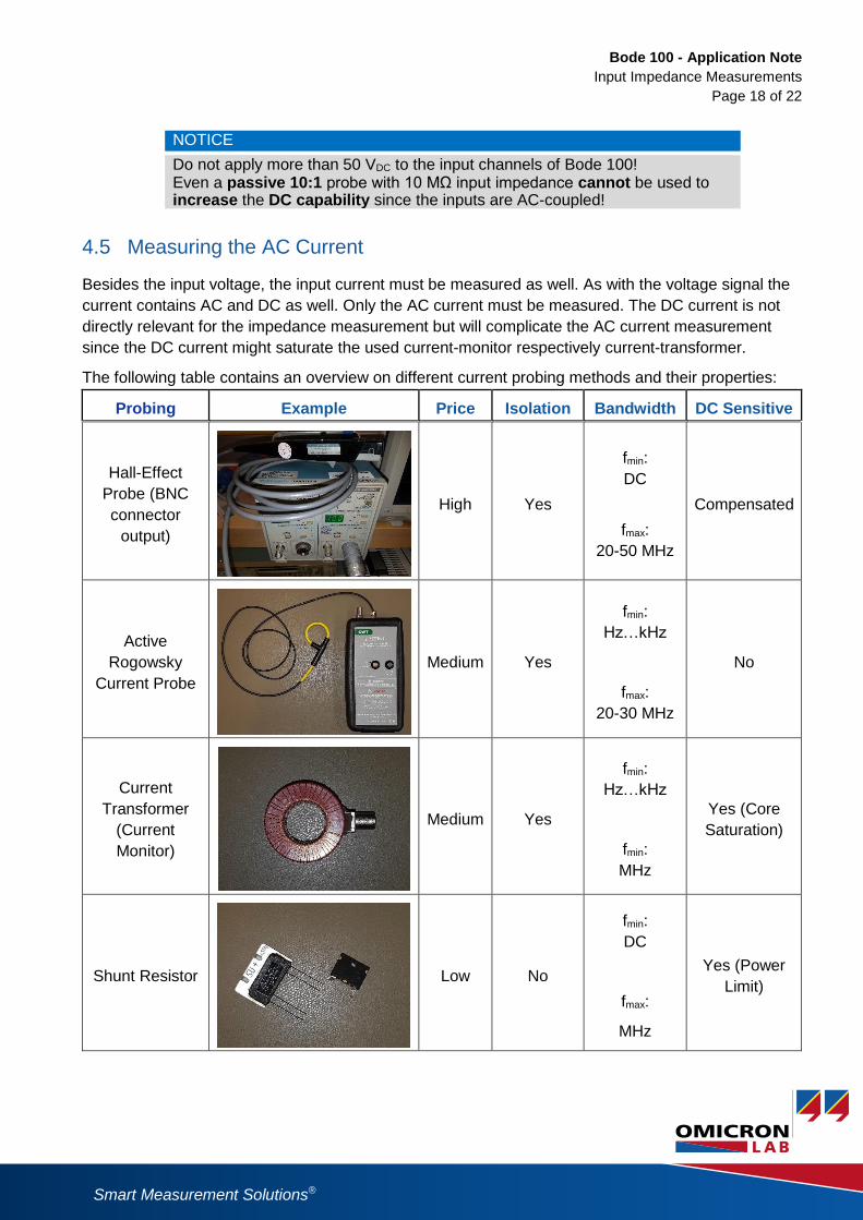
4.5 Measuring the AC Current
Besides the input voltage, the input current must be measured as well. As with the voltage signal the
current contains AC and DC as well. Only the AC current must be measured. The DC current is not
directly relevant for the impedance measurement but will complicate the AC current measurement
since the DC current might saturate the used current-monitor respectively current-transformer.
The following table contains an overview on different current probing methods and their properties:
Probing Example Price Isolation Bandwidth DC Sensitive
Hall-Effect
Probe (BNC
connector
output)
High Yes
fmin:
DC
fmax:
20-50 MHz
Compensated
Active
Rogowsky
Current Probe
Medium Yes
fmin:
Hz…kHz
fmax:
20-30 MHz
No
Current
Transformer
(Current
Monitor)
Medium Yes
fmin:
Hz…kHz
fmin:
MHz
Yes (Core
Saturation)
Shunt Resistor
Low No
fmin:
DC
fmax:
MHz
Yes (Power
Limit)
Bode 100 - Application Note
Input Impedance Measurements
Page 19 of 22
Smart Measurement Solutions
Smart Measurement Solutions®
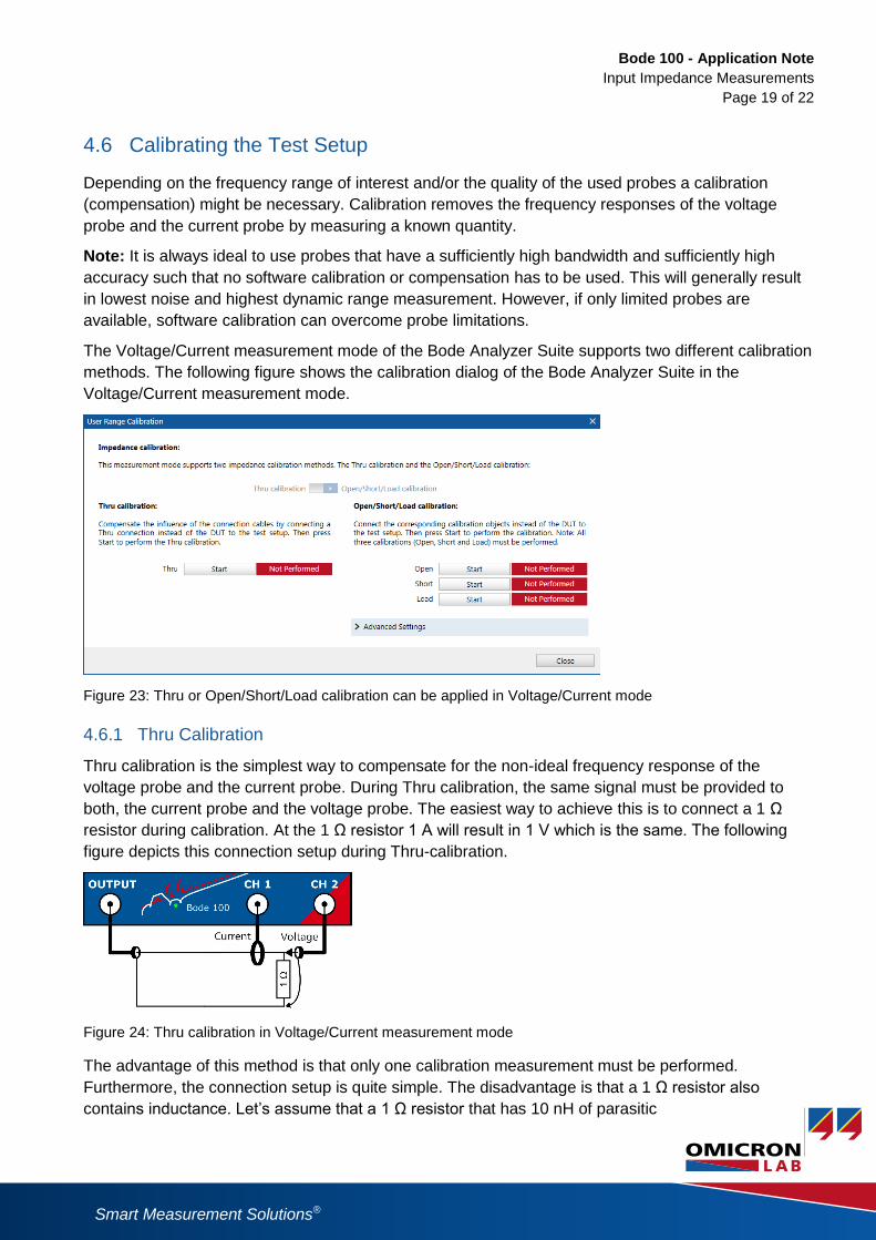
4.6 Calibrating the Test Setup
Depending on the frequency range of interest and/or the quality of the used probes a calibration
(compensation) might be necessary. Calibration removes the frequency responses of the voltage
probe and the current probe by measuring a known quantity.
Note: It is always ideal to use probes that have a sufficiently high bandwidth and sufficiently high
accuracy such that no software calibration or compensation has to be used. This will generally result
in lowest noise and highest dynamic range measurement. However, if only limited probes are
available, software calibration can overcome probe limitations.
The Voltage/Current measurement mode of the Bode Analyzer Suite supports two different calibration
methods. The following figure shows the calibration dialog of the Bode Analyzer Suite in the
Voltage/Current measurement mode.
Figure 23: Thru or Open/Short/Load calibration can be applied in Voltage/Current mode
4.6.1 Thru Calibration
Thru calibration is the simplest way to compensate for the non-ideal frequency response of the
voltage probe and the current probe. During Thru calibration, the same signal must be provided to
both, the current probe and the voltage probe. The easiest way to achieve this is to connect a 1 Ω
resistor during calibration. At the 1 Ω resistor 1 A will result in 1 V which is the same. The following
figure depicts this connection setup during Thru-calibration.
Figure 24: Thru calibration in Voltage/Current measurement mode
The advantage of this method is that only one calibration measurement must be performed.
Furthermore, the connection setup is quite simple. The disadvantage is that a 1 Ω resistor also
contains inductance. Let’s assume that a 1 Ω resistor that has 10 nH of parasitic
Bode 100 - Application Note
Input Impedance Measurements
Page 20 of 22
Smart Measurement Solutions
Smart Measurement Solutions®
inductance is used. This will introduce a measurement error of 6 % at 1 MHz due to the reactance
added by the 10 nH parasitic inductance.
4.6.2 Open/Short/Load Calibration
Open/Short/Load calibration offers the highest accuracy over the widest frequency range and
compensates more effects than the Thru calibration. A major disadvantage however is that not every
test setup can be used to perform e.g. a Short calibration. This is especially the case if the DC portion
of the signal cannot be removed during calibration.
The following figure shows the three states that must be measured to perform an Open/Short/Load
calibration.
Figure 25: Open/Short/Load calibration in Voltage/Current measurement mode
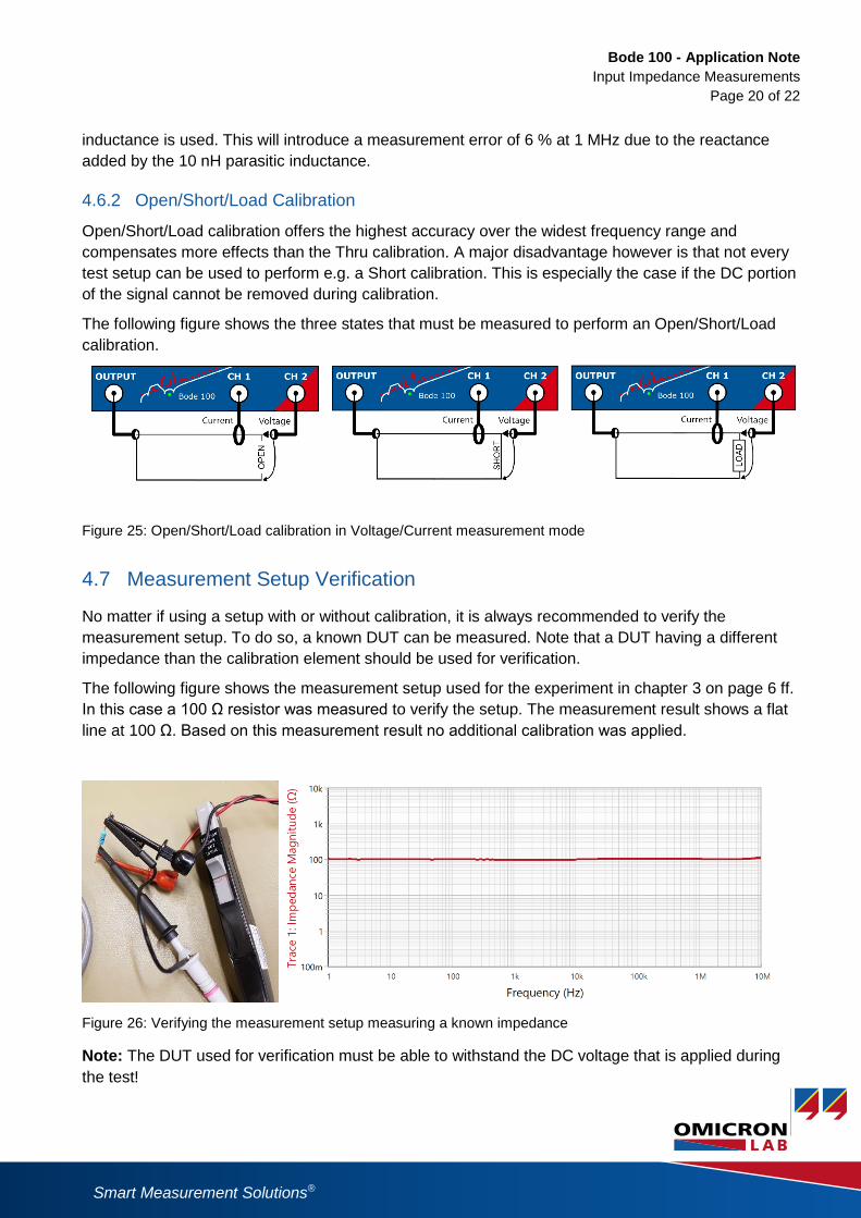
4.7 Measurement Setup Verification
No matter if using a setup with or without calibration, it is always recommended to verify the
measurement setup. To do so, a known DUT can be measured. Note that a DUT having a different
impedance than the calibration element should be used for verification.
The following figure shows the measurement setup used for the experiment in chapter 3 on page 6 ff.
In this case a 100 Ω resistor was measured to verify the setup. The measurement result shows a flat
line at 100 Ω. Based on this measurement result no additional calibration was applied.
Figure 26: Verifying the measurement setup measuring a known impedance
Note: The DUT used for verification must be able to withstand the DC voltage that is applied during
the test!
Bode 100 - Application Note
Input Impedance Measurements
Page 21 of 22
Smart Measurement Solutions
Smart Measurement Solutions®
5 Summary
In the past, power supply stability analysis has been performed mainly in space applications [7], [8]
that include complex DC power distribution systems with multiple regulators and different DC power
bus levels.
Today complex power electronic systems are becoming widely spread in many application fields such
as embedded system design and electric vehicle drive trains. To avoid stability problems in the field,
stability should be considered during the development process of power electronic systems.
The input impedance of a DC/DC converter is a critical design parameter for stability. Measuring the
input impedance is a simple possibility to either evaluate a black-box converter system or to prove
simulation results. Converter input impedance and converter output impedance together with filter
impedance are critical parameters that must be considered when connecting multiple regulators and
filters to form a power distribution system. Improper impedance ratios can result in system instability.
Bode 100 in combination with the Bode Analyzer Suite offers an advanced platform for any power
system impedance measurement. With the flexible hardware and software design, a high variety of
test-setups are supported. The high noise rejection and dynamic range of the Bode 100 makes it the
perfect choice for power system impedance measurements. Together with the Bode Analyzer Suite,
Bode 100 is a powerful tool that should not be missing on a power electronic engineer’s bench.
6 References
[1] R. D. Middlebrook, “Null double injection and the extra element theorem,” IEEE Trans. Educ., vol. 32, no. 3, pp. 167–180, Aug. 1989.
[2] R. D. Middlebrook, “Input filter considerations in design and application of switching regulators,” IEEE Conf Rec Annu Meet Ind Appl Soc, vol. 11th, pp. 366–382, 1976.
[3] R. W. Erickson and D. Maksimovic, Fundamentals of Power Electronics, 2nd ed. 2001. Norwell, Mass.: Springer, 2001.
[4] Venable, “Minimizing Input Filter Requirements in Military Power Supply Designs.” Venable.
[5] R. W. Erickson, “Optimal single resistors damping of input filters,” in Applied Power Electronics Conference and Exposition, 1999. APEC ’99. Fourteenth Annual, 1999, vol. 2, pp. 1073–1079 vol.2.
[6] Y. Panov and M. Jovanovic, “Practical issues of input/output impedance measurements in switching power supplies and application of measured data to stability analysis,” in Twentieth Annual IEEE Applied Power Electronics Conference and Exposition, 2005. APEC 2005., 2005, vol. 2, p. 1339–1345 Vol. 2.
[7] M. Komatsu and S. Yanabu, “Analysis of the small signal stability for the international space station/JEM electric power systems,” in 2008 IEEE 2nd International Power and Energy Conference, 2008, pp. 106–111.
[8] E. W. Gholdston, K. Karimi, F. C. Lee, J. Rajagopalan, Y. Panov, and B. Manners, “Stability of large DC power systems using switching converters, with application to the International Space Station,” in IECEC 96. Proceedings of the 31st Intersociety Energy Conversion Engineering Conference, 1996, vol. 1, pp. 166–171 vol.1.

Bode 100 - Application Note
Input Impedance Measurements
Page 22 of 22
Smart Measurement Solutions
Smart Measurement Solutions®
Americas
OMICRON electronics Corp. USA
Phone: +1 713 830-4660
Fax: +1 713 830-4661
Asia Pacific
OMICRON electronics Asia Limited
Phone: +852 3767 5500
Fax: +852 3767 5400
Europe, Middle East, Africa
OMICRON electronics GmbH
Phone: +43 59495
Fax: +43 59495 9999
[email protected] www.omicron-lab.com
OMICRON Lab is a division of OMICRON electronics specialized in
providing Smart Measurement Solutions to professionals such as
scientists, engineers and teachers engaged in the field of electronics.
It simplifies measurement tasks and provides its customers with more
time to focus on their real business.
OMICRON Lab was established in 2006 and is meanwhile serving
customers in more than 50 countries. Offices in America, Europe, East
Asia and an international network of distributors enable a fast and
extraordinary customer support.
OMICRON Lab products stand for high quality offered at the best
price/value ratio on the market. The products' reliability and ease of use
guarantee trouble-free operation. Close customer relationship and more
than 30 years in-house experience enable the development of
innovative products close to the field.