Embed Size (px)
Citation preview
InP AND GaAs COMPONENTS FOR 40 Gbps APPLICATIONS
M. Siddiqui, G. Chao, A. Oki, A. Gutierrez-Aitken, B. Allen, A. Chau, W. Beall, M. D’Amore, B. Oyama, D. Hall, R Lai, and D. Streit
Velocium, a TRW Company
2221 Park Place El Segundo, CA 90245
Abstract - We have developed a number of products for 40 Gbps applications, including InP-based monolithically integrated PIN-TIA circuits, GaAs HEMT modulator drivers, InP double heterojunction digital circuits, HBT TIAs, and high responsivity dual-absorption PIN diodes. Other products include integrated TIAs and limiting amplifiers as well as CDRs and CMUs with MUX and DeMUX’s
I. INTRODUCTION The development of OC-768 fiber optics is being paced by both market requirements and product availability. A push to obtain cost-effective solutions for 40 Gbps is being realized. The success criteria for OC-768 is that the cost for 40 Gbps equipment must not be more than about 2.5 times the cost of 10 Gbps equipment. We are using high-volume GaAs and InP production processes to obtain 40 Gbps solutions that are both high performance and cost effective. We describe here the products we have already developed for 40 Gbps applications, as well as those ready for near-term introduction.
II. MODULATOR DRIVER We have developed a HEMT-based modulator driver for 40 Gbps and beyond (1). Using the 0.1 µm gate-length GaAs PHEMT process, a distributed amplifier that demonstrates over 12.5 dB gain up to 50 GHz with as much as 23 dBm output power was developed. This high output power shows the amplifier's capability of providing the large voltage swing that is required to drive an external optical modulator. TRW's 0.1 µm GaAs HEMT MMIC process is unique towards simultaneously providing high bandwidth and high power capability for this application. The process features high cutoff frequency at high drain voltage operation with fT > 110 GHz up to 4V operation, and proven reliable operation at these conditions. Thousands of 0.1 µm HEMT wafers have been fabricated at TRW, and the first pass design success of
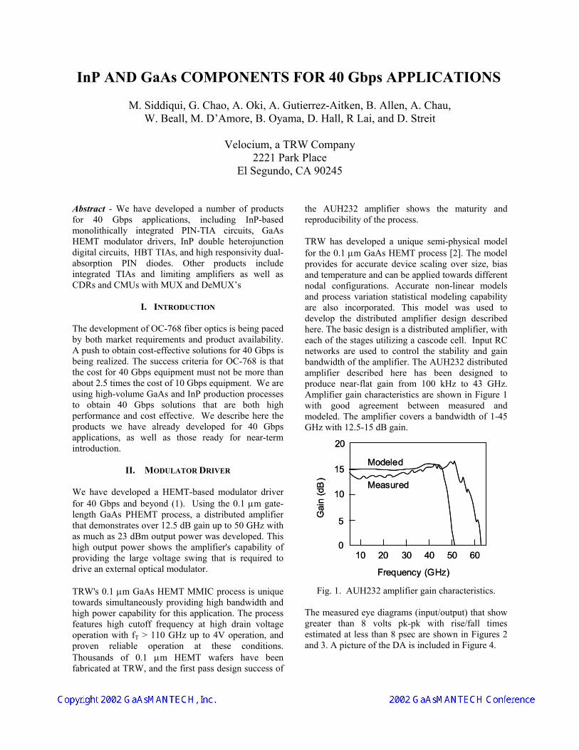
the AUH232 amplifier shows the maturity and reproducibility of the process. TRW has developed a unique semi-physical model for the 0.1 µm GaAs HEMT process [2]. The model provides for accurate device scaling over size, bias and temperature and can be applied towards different nodal configurations. Accurate non-linear models and process variation statistical modeling capability are also incorporated. This model was used to develop the distributed amplifier design described here. The basic design is a distributed amplifier, with each of the stages utilizing a cascode cell. Input RC networks are used to control the stability and gain bandwidth of the amplifier. The AUH232 distributed amplifier described here has been designed to produce near-flat gain from 100 kHz to 43 GHz. Amplifier gain characteristics are shown in Figure 1 with good agreement between measured and modeled. The amplifier covers a bandwidth of 1-45 GHz with 12.5-15 dB gain.
10 20 30 40 50 60
Frequency (GHz)
0
10
20
5
15
Gai
n (d
B)
Modeled
Measured
10 20 30 40 50 60
Frequency (GHz)
0
10
20
5
15
Gai
n (d
B)
Modeled
Measured
Fig. 1. AUH232 amplifier gain characteristics. The measured eye diagrams (input/output) that show greater than 8 volts pk-pk with rise/fall times estimated at less than 8 psec are shown in Figures 2 and 3. A picture of the DA is included in Figure 4.
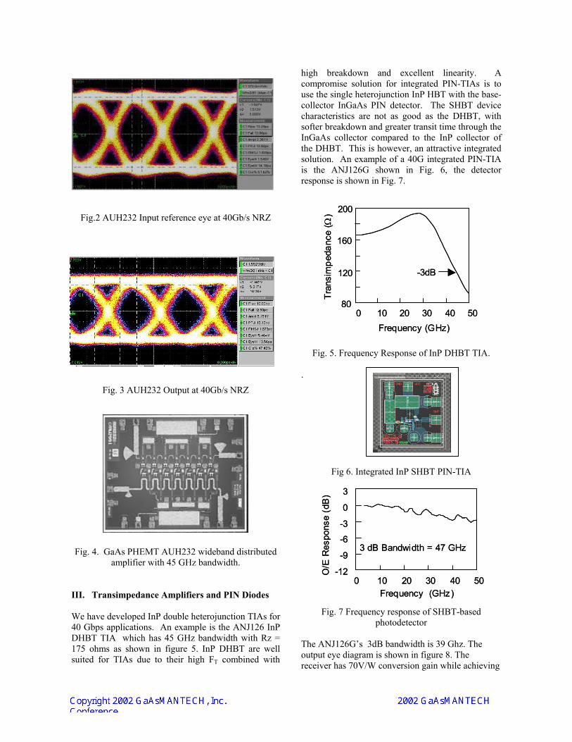
Fig.2 AUH232 Input reference eye at 40Gb/s NRZ
Fig. 3 AUH232 Output at 40Gb/s NRZ Fig. 4
III. T
We hav40 GbpDHBT175 ohsuited
high breakdown and excellent linearity. A compromise solution for integrated PIN-TIAs is to use the single heterojunction InP HBT with the base-collector InGaAs PIN detector. The SHBT device characteristics are not as good as the DHBT, with softer breakdown and greater transit time through the InGaAs collector compared to the InP collector of the DHBT. This is however, an attractive integrated solution. An example of a 40G integrated PIN-TIA is the ANJ126G shown in Fig. 6, the detector response is shown in Fig. 7.
80
120
160
200
Tran
sim
peda
nce
(Ω)
0 10 20 30 40 50Frequency (GHz)
-3dB
80
120
160
200
Tran
sim
peda
nce
(Ω)
0 10 20 30 40 50Frequency (GHz)
-3dB
Fig. 5. Frequency Response of InP DHBT TIA. .
. GaAs PHEMT AUH232 wideband distributed amplifier with 45 GHz bandwidth.
ransimpedance Amplifiers and PIN Diodes
e developed InP double heterojunction TIAs for s applications. An example is the ANJ126 InP
TIA which has 45 GHz bandwidth with Rz = ms as shown in figure 5. InP DHBT are well for TIAs due to their high FT combined with
Fig 6. Integrated InP SHBT PIN-TIA
-12
-9
-6-3
0
3
0 10 20 30 40 5Frequency (GHz)
O/E
Res
pons
e (d
B)
3 dB Bandwidth = 47 GHz
-12
-9
-6-3
0
3
0 10 20 30 40 5Frequency (GHz)
O/E
Res
pons
e (d
B)
3 dB Bandwidth = 47 GHz
00
Fig. 7 Frequency response of SHBT-based photodetector
The ANJ126G’s 3dB bandwidth is 39 Ghz. The output eye diagram is shown in figure 8. The receiver has 70V/W conversion gain while achieving

error free operation with < –7dBm (2^23-1 PN coded) input.
Fig. 8. Output Eye Diagram
IV. HIGH RESPONSIVITY PINIP PHOTODETECTOR
We have developed an In GaAs dual-absorption PINIP diode that has significant advantages for 40 Gbps and higher applications. The device eliminates the trade-off in design characteristics between high responsivity and high bandwidth. The key idea in this photodiode is to integrate two absorption regions using a transparent contact layer in the center, as shown in Fig. 9. The photocurrents generated in both of the absorption regions are combined to increase the responsivity of the device, while the transit time of the carriers remains the same since the carriers are collected separately from each absorption region. While the capacitance of the detector is twice that of a single detector, this is not an issue for high frequency applications because for small area diodes transit time dominates detector frequency response. Using the first generation of this device we have achieved responsivity of 1.04 A/W with a bandwidth of 30 GHz. The circuit schematic for the PINIP device is shown in Fig. 10. Analysis of these results leads us to believe that devices optimized for 40 GHz applications will have responsivity > 0.8 A/W. This high responsivity is key to achieve good photodetector sensitivity. While waveguide photodetectors also eliminate transit time and responsivity compromises, they are typically difficult to couple due to the small size of the waveguide. The dual-absorption PINIP detector will simplify packaging compared to the waveguide detectors, and promises an elegant solution to the traditional PIN diodes.
InP Substrate
p+ contact layer
n+ transparent contact
n- InGaAs
n- InGaAs
n+ contact layer
InP Substrate
p+ contact layer
n+ transparent contact
n- InGaAs
n- InGaAs
n+ contact layer
Fig. 9. Profile of high-responsivity PINIP photodetector.
C2
R2
2
C1
R1
1I
I C2
R2
2
C1
R1
1I
I
Fig. 10. Schematic of PINIP device.
V. INP DHBT DIGITAL CIRCUITS
InP DHBT is a natural solution to the problem of 40 Gbps digital requirements. We are in our second iteration of a full physical layer chip set including PN generator, 1:4 MUX, 4:1 DEMUX, Clock Recovery Loop, and X4 PLL multiplier. In addition, several smaller circuits were developed including NRZ-RZ converter at 12.5 G, a high sensitivity 25G Div. By 2 as well as a 50 G Divide by 2. The first iteration of the 4:1 MUX operates up to 45Gb/s taking in 4 streams of 10G data. It uses a half rate clock with internal retiming. We have combined it with a PN generator for ease of testing. The PN generator creates 4 streams of 10g data with 2^4 PN code. This was done to eliminate the need for an expensive data generator during initial testing. The 1:4 DEMUX also operates up to 45Gb/s. The MUX/DEMUX photographs are included in Figures 11 and 12. The eye diagram showing the performance of the MUX/DEMUX pair is shown in Figure 12. The figure shows four 10 Gb/s streams of data after going through a 4:1 and 1:4 MUX/DEMUX back-to-back. Included in the first iteration chips are the CDR and CMU IC’s that are currently under test. Also under development are the following single function IC’s: VCO at 20 and 40

Ghz, 40G divide by 4, 2.5 G phase detectors, D flip flops at 40 G, fan out buffers and EXOR gate, both at 20G.
Fig. 11. InP DHBT 4:1 Mux.
Fig. 12. InP DHBT 1:4 Demux.
FIG. 13
VI. RELIABILITY One of the key ingredients for long-term success in telecommunication applications is the ability to achieve high reliability for all parts. We have space-qualified GaAs HEMT and InP HEMT processes, and we are now qualifying our InP HBT process. The results for the GaAs HEMT and InP HEMT have been presented in (2) and (3), with MTF > 107 h at 125C. Our InP DHBT integrated circuits have achieved in-process reliability of MTF > 4x 10⁸ hours at 125C, with an activation energy of 1.9 eV, at a current density of Jc = 120 kA/cm2. This translates to junction temperatures of 220°C. The qualification vehicle is an InP DHBT log amp, with 5 stages of amplification and 6 stages of detection, as shown in Fig. 14. This circuit is extremely sensitive to changes in beta, Vbe, emitter resistance, and to passive element value changes. The circuit includes Schottky diodes, MIM capacitors, thin film resistors, airbridge interconnect and backside vias. The advantage of qualifying an integrated circuit is obvious in that all components are evaluated simultaneously.
Fig. 14. InP DHBT logarithmic amplifier.
. 10 GB/SEC DATA FROM BACK-TO-BACK MUX/DEMUX.
10
8
107
Jc = 120 kA/cm2
125o
C MTF > 108
h
Ea ~ 1.9 eV 10
6
105
MTF (h)
104
103
102
101
1.5 1.75 2.0 2.25 2.5 1000/T (1/K)
Fig. 15. Arrenhious plot of InP DHBT log amp in-process reliability results.
VII. SUMMARY
OC768 systems will require cost effective high performance, high reliability solutions to the photonic and electronic requirement .We are building a broad range of products to address the 40 Gbps market in a high-volume process that will allow efficiencies of scale to be applied to this market. These products include GaAs PHEMT mod drivers today, and soon improved InP HEMT drivers. Monolithic PIN-TIAs achieve integration efficiency and newer high responsivity detectors will improve sensitivity. Digital products using improved high-yield InP DHBT processes will soon be available, and will compete in both power and cost with silicon solutions, while providing full rate rather than half rate clocks. The reliability of these processes has been fully tested and proven time and again for TRW's space applications. The drive to 40 Gbps is both capacity-based and cost-based, applying proven high-volume high-performance process solutions to 40 Gbps requirements will enable this market.
Acknowledgements We gratefully acknowledge the contributions of the InP design, layout, and processing teams at TRW and Velocium, including Frank Yamada, Tom Block, Jeff Elliott, Scott Olson, and Donald Umemoto. We also thank the module evaluation team including Leo Callejo, David Cisneros and Jennifer Battle.
References
(1) D. Streit, et. Al., “InP and GaAs Components for 40GBPS Applications,” 2002 GaAs IC Symposium Tech. Digest, pgs 247 – 250. (2) R. Lai, et. al., "0.1 µm InGaAs/AlGaAs/GaAs HEMT MMIC production process for Ka-band LNAs," Proceedings 2000 International Conference on Gallium Arsenide Manufacturing Technology, pp. 249-250, 2000. (3) A. Gutierrez-Aitken, "Responsivity Photodetector," US Patent 6043549, Mar. 28, 2000 (4) A. Gutierrez-Aitken, et. al., "Ultra High Speed Direct Digital Synthesizer Using InP DHBT Technology," proceedings of 2001 GaAs IC Symposium.


![Convection interaction in GaAs/LEC growth modelcrystal structure due to the formation of facets on the oxides growth interface [5]. In the case of semiconductors such as GaAs and InP,](https://img.dokumen.tips/doc/110x75/5f8c6f31cd9ef24dc9575a6e/convection-interaction-in-gaaslec-growth-crystal-structure-due-to-the-formation.jpg)

![LIST OF PUBLICATIONSshodhganga.inflibnet.ac.in/bitstream/10603/11617/5... · LIST OF PUBLICATIONS Journals Included in the Thesis [1] Observation of electron confinement in InP/GaAs](https://img.dokumen.tips/doc/110x75/5ec805791d45222e6334df55/list-of-pu-list-of-publications-journals-included-in-the-thesis-1-observation.jpg)


