Embed Size (px)
DESCRIPTION
Wireless Power
Citation preview
IEEE TRANSACTIONS ON POWER ELECTRONICS, VOL. 30, NO. 2, FEBRUARY 2015 817
Innovative 5-m-Off-Distance Inductive PowerTransfer Systems With Optimally
Shaped Dipole CoilsChangbyung Park, Student Member, IEEE, Sungwoo Lee, Gyu-Hyeong Cho, Senior Member, IEEE,
and Chun T. Rim, Senior Member, IEEE
Abstract—5-m-off-distance inductive power transfer systemsthat have optimally shaped cores in the primary and secondarycoils are proposed. Instead of conventional-loop-type coils for mag-netic resonance scheme, magnetic dipole type coils with cores areused for drastic reduction in deployment space and quite longwireless power transfer. An optimized stepped core structure isalso proposed, where a strong magnetic field section is so thick thatmagnetic field density may be even. Thus, the proposed optimizedstepped core has only 41% core loss compared with an unoptimizedeven core but delivers 2.1 times more wireless power for a givenamount of core. Experimentally obtained maximum output pow-ers and primary-coil-to-load-power efficiencies for 3, 4, and 5 m at20 kHz were 1403, 471, 209 W, and 29%, 16%, 8%, respectively.
Index Terms—Inductive coupling, inductive power transfer sys-tem (IPTS), wireless power.
I. INTRODUCTION
EXTENDING the distance of wireless power has a long his-tory beginning with Nikola Tesla trying to make an electric
power grid without wires [1]. In 2007, a wireless power trans-fer scheme using strongly coupled magnetic resonance systems(CMRS) was introduced whose power transfer level and coil-to-coil efficiency are 60 W and 45%, respectively, at a distanceof 2 m [2]. CMRS adopted large self-resonant coils at eachprimary and secondary side to induce a large magnetic field toobtain an extended transfer range. For the high current in theseself-resonant coils, the internal resistances of the coils must bevery small. This means that the coils must have very high Qfactors, which consequently result in very thick wires. The highQ factors also result in substantial voltage stresses on the coils
Manuscript received October 21, 2013; revised January 5, 2014; acceptedFebruary 22, 2014. Date of publication March 11, 2014; date of current versionOctober 7, 2014. This paper was presented in part at the ECCE-ASIA 2012. Thiswork was supported by the National Research Foundation of Korea Grant fundedby the Korea government (MEST) under Grant 2010-0029179, and also by theNuclear Power Core Technology Development Program of KETEP, granted fi-nancial resource from the Ministry of Trade, Industry, and Energy, Republic ofKorea (20121610100030). Recommended for publication by Associate EditorU. K. Madawala.
C. Park and G.-H. Cho are with the Department of Electrical Engineering,Korea Advanced Institute of Science and Technology, Daejeon 305-755, Korea(e-mail: [email protected]; [email protected]).
S. Lee is with Samsung Electronics, Yong-in 446-711, Korea (e-mail:[email protected]).
C. T. Rim is with the Department of Nuclear and Quantum Engineering,Korea Advanced Institute of Technology, Daejeon 305-755, Korea (e-mail:[email protected]).
Color versions of one or more of the figures in this paper are available onlineat http://ieeexplore.ieee.org.
Digital Object Identifier 10.1109/TPEL.2014.2310232
because the coils should sustain Q times larger reactive currentor voltage than the corresponding current or voltage of the realpower. For example, 1 MVA rating of coil is required to deliver400 W for Q = 2500. To sustain high voltage stress among wiresin the coil, the coils cannot help being bulky with large air gapbetween adjacent wires. Furthermore, the resonant frequenciesof the coils are not set by lumped capacitors and inductors butby their inherent stray capacitances and inductances. The straycapacitances and inductances are too sensitive to surroundingssuch as temperature, humidity, and human proximity [3], [4].With high Q factors that result in extremely narrow resonantfrequency bandwidth and moving resonant frequency due toenvironmental sensitivity, a complicated automated matchingsystem is needed to track and tune up the resonant condition ofthe high Q coils using switched inductors and capacitors [5], [6].Even though a tuning up scheme is applied, matching the mul-tiple resonant coils with high environmental sensitivity is ex-tremely difficult in practice. Due to the distributed coil structureof parasitic capacitance and inductance, the operating frequencyof the CMRS tends to be of the order of 10 MHz, which resultsin the use of RF power amplifiers rather than efficient switch-ing converters [6]. The CMRS for 60-W power transferred overthe distance of 50 cm has an apparently high coil-to-coil ef-ficiency of 80% [7]; however, its system efficiency includingpower source and ac–dc conversion would be quite low. Thesecharacteristics are why the well-known CMRS is seldom usedin high-power applications. Therefore, inductive power transfersystems (IPTS) have been widely used [8]–[35] for applicationsthat consume more than tens of watt.
In this paper, an IPTS driven by an inverter of 20-kHz switch-ing frequency for 5-m-off distance is proposed. Magnetic dipolecoils of narrow and long structure, having ferrite cores inside, areadopted for the primary and secondary coils, minimizing par-asitic effects [35]. Optimum-stepped core structures that mini-mize core loss for a given amount of ferrite material are newlyproposed. It is verified by simulations, analyses, and experi-ments for 20 and 105 kHz that the IPTS, which has been, so far,believed to be adequate for proximity wireless power transferonly, is quite suitable for long distance power delivery as well.
II. PRIMARY AND SECONDARY COIL DESIGN
A. Overall Coil Configuration
The overall configuration of the IPTS, which is composedof an inverter, capacitor banks, a rectifier, and load as well as
0885-8993 © 2014 IEEE. Personal use is permitted, but republication/redistribution requires IEEE permission.See http://www.ieee.org/publications standards/publications/rights/index.html for more information.
818 IEEE TRANSACTIONS ON POWER ELECTRONICS, VOL. 30, NO. 2, FEBRUARY 2015
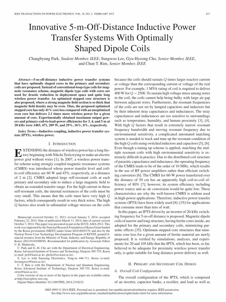
Fig. 1. Overall configuration of the proposed IPTS including primary andsecondary coils.
Fig. 2. Simulation result of the magnetic flux lines of the proposed coil con-figuration, where d = 3 m, I1 = 10 A.
proposed primary and secondary coils, is shown in Fig. 1. Theprimary and secondary windings are wound around the center ofprimary and secondary cores, and its winding shape is analogousto a helical coil. Each winding is composed of a litz wire toreduce the ac series resistance of the coils. The current of theprimary winding generates magnetic field, and then the linkagemagnetic flux induces the voltage at the secondary winding.
If an air coil were used, the inner part of the coil would havelarge magnetic reluctance whereas the outer part of it would haverelatively very small magnetic reluctance because of the largeeffective field crossing area of the outer part of the coil. Strongmagnetic field generation, which is crucial for longer distancepower delivery, is limited by the large magnetic reluctance ofthe inner part of the air coil. To reduce this magnetic reluctance,a long rod-type ferrite core is inserted into the air coil, as shownin Fig. 1. As a rule of thumb, this ferrite coil generates about50 times stronger magnetic field intensity than the air coil bymeans of the magnetic reluctance reduction.
Magnetic flux lines between the primary and secondary coilsare shown in Fig. 2, representing that parts of magnetic fluxlines are effectively interlinked to the secondary coil. To make alarger linkage flux, a longer ferrite rod should be inserted. Thesimulations, throughout this paper, were performed by AnsoftMaxwell v14.0.
Fig. 3. Simulation results of the magnetic flux density at the center of thesecondary coil for the primary and secondary core length lc (1–6 m) and variousdistances d (2–5 m). lc = 3 m was selected as the baseline design in this paper.
The rms value of the induced voltage of the secondary coilV2 is proportional to the rms value of the magnetic flux crossingits winding B2(x) as follows:
V2 = ωB2(x)A2N2 (1)
where the winding is evenly distributed, ω is the angular switch-ing frequency, A2 is the cross-sectional area of the secondarycoil near center lh2 · lt2 , N2 is the number of turns of the sec-ondary coil, and the averaged magnetic flux density over thewinding length lw is determined as follows:
B2(x) ≡ 1lw
∫ lw /2
−lw /2B2(x)dx. (2)
The simulated magnetic flux density at the center of the sec-ondary coil B2(0) versus the primary and secondary core lengthlc for various distances d is shown in Fig. 3, where the corelengths of the primary and secondary cores are assumed to besame. The longer core length is, the larger magnetic flux den-sity in the secondary core is. For a longer distance of powertransfer, the core should be lengthened. As shown in Fig. 3,the core length of 1–2 m is too short for 5-m-off power trans-fer because of the very low magnetic flux density; however, itbecomes considerably increased if the core length is 3 m.
Concerning the winding length lw , the magnetic linkage fluxpassing through the secondary winding increases as lw de-creases, as shown in Fig. 2; hence, lw = 0 is the optimumcondition for maximizing the induced voltage, as was identifiedfrom (2) as follows:
Max{
B2(x)}
= limlw →0
1lw
∫ lw /2
−lw /2B2(x)dx = B2(0)
= Max {B2(x)} . (3)
In practice, (3) cannot be realized because the narrowed wind-ing length deteriorates the frequency response due to parasiticcapacitances between each coil winding and between core andwinding, respectively, as shown in Fig. 9. Furthermore, local

PARK et al.: INNOVATIVE 5-M-OFF-DISTANCE INDUCTIVE POWER TRANSFER SYSTEMS WITH OPTIMALLY SHAPED DIPOLE COILS 819
Fig. 4. Simulated magnetic flux density for the primary coil with even thick-ness of ferrite core lt1 = 7 cm, when lc = 3 m and lw = 1 m. The number ofturns is 22 and the primary current I1 is 40 Arm s to reach the saturation levelof 190 mT.
Fig. 5. Magnetic flux density profile of the proposed stepped core. x1 , x2 , x3 ,and x4 denote the junctions of each stepped core.
core saturation may occur for a large secondary current due toconcentrated magnetic flux if lw is too small.
B. Optimized Design of the Proposed Stepped Core
Conventional ferrite material has a saturation flux density ofabout 300 mT at room temperature, but practically, the maxi-mum should be less than 200 mT considering the core loss andtemperature increase of the material due to the loss. The highertemperature of the ferrite material decreases the saturation fluxdensity. If the thickness of the ferrite core along the x-axis iseven, the magnetic flux density profile in the ferrite core is notuniform along the longitudinal line (x-axis), as shown in Fig. 4.This uneven profile can be easily anticipated from Fig. 2, wherethe magnetic linkage of each side is concentrated at the centerof the core; hence, the magnetic flux density becomes highestatthe center of the core and gradually decreases for the outer sec-tion. Therefore, the lower magnetic field section of other partsdoes not have to be thick. Even though applicable to the sec-ondary coil, this optimum core design, in this paper, is focusedon the primary coil, which undergoes severe core saturation forgenerating high magnetic flux.
As shown in Fig. 4, the ampere-turn of the primary coil isfound to be 880 [Amp turn] by simulation with the configurationof lh1 = 20 cm and lt1 = 7 cm, i.e., A1 = 140 cm2 to reach
Fig. 6. Magnetic flux distribution at the stepped junction of the ferrite core.Magnetic flux density change is plotted at the bottom.
the magnetic saturation level of 190 mT. Now, the current levelof the primary coil I1 was chosen as 40 Arms , considering thecurrent rating of an available inverter; however, it could be sofar as the ampere-turn is met. Then, the number of turns of theprimary coil N1 was determined as 22.
The ferrite core thickness should be optimized considering themagnetic field profile. If the total amount of the ferrite material isgiven, the outer section needs to be thinner so that the magneticflux density can be uniform. A simple optimum design rule foruniform magnetic flux density is to make the core cross-sectionalarea as follows:
A1opt(x) =A1(0)B1(0)
B1(x) (4)
where A1(0) and B1(x) are the cross-sectional area and mag-netic flux density, respectively, of the even thickness core, asshown in Fig. 6. Under the condition of (4), the magnetic fluxdensity of the proposed optimized core becomes the following:
B1opt(x) =B1(x)A1(0)A1opt(x)
=B1(0)A1(0)
≡ B0
A1(0)= constant.
(5)In other words, if the cross-sectional area is of the same form
of magnetic flux density profile of the even thickness core, thenuniform magnetic flux density can be obtained.
For fabrication purposes, however, the core length should befinitely segmented, as shown in Fig. 5, where half of the coreis presented due to symmetry of the coil. This stepped shapeconfiguration can be easily implemented by small-size ferriteblocks, where the thickness of a block is now 2 cm. It hasbeen assumed that the magnetic flux density profile B1(x) isunchanged even though A1opt(x) is changed, which shall bevalid for the case of this paper where the core thickness is muchless than the core length.
The optimization can be done by finding the longitudinal(x-axis) points x1 , x2 , x3 , and x4 , where the magnetic flux den-sity at each stepped junction reaches the maximum value B0 . Inthis paper, five segmentations were assumed.
Different from conventional air coils, the exact calculationof the magnetic flux density in the proposed ferrite-core coil ishardly possible, and measuring the magnetic flux density in the

820 IEEE TRANSACTIONS ON POWER ELECTRONICS, VOL. 30, NO. 2, FEBRUARY 2015
ferrite core is impossible. In this paper, the simulated magneticflux density profile, as shown in Fig. 4, is numerically modeled,considering the curved and straight line portions, as follows:
B1(x) =
⎧⎪⎪⎨⎪⎪⎩
Bw (x) = B0{1 − c0 |x|n}, for|x| < lw /2 wound section (6a)
Bu (x) = a0(|x| − x1) + b0 , forlw /2 < |x| < lc/2 unwound section (6b)
where x1≈lw /2 and the coefficients are determined from Fig. 5as follows:
a0 = − Bw (x1)lc/2 − x1
, b0 = Bw (x1) (7a)
c0 = 0.9, n = 2.0. (7b)
In (7b), the c0 and n are obtained by curve fitting from Fig. 5.Similar with (5), an optimized magnetic flux density profile
for the stepped core can also be found by approximating theprofile to the even magnetic flux density B1(0). The optimizedmagnetic flux density profile function is then as follows:
B1opt(x) = B10(x) + B11(x) + B12(x) + B13(x) + B14(x)(8)
where
B10(x) = Bw (x), for 0 ≤ |x| < x1 (9a)
B11(x) = a1(|x| − x1) + b1 , for x1 ≤ |x| < x2 (9b)
B12(x) = a2(|x| − x2) + b2 , for x2 ≤ |x| < x3 (9c)
B13(x) = a3(|x| − x3) + b3 , for x3 ≤ |x| < x4 (9d)
B14(x) = a4(|x| − x4) + b4 , for x4 ≤ |x| < lc/2. (9e)
In (9), what should be determined are 12 constants, i.e., ai’s,bi’s, and xi’s.
First, bi’s are easily found, considering the fact that the initialvalue of each B1i(xi) should be the same as B0 , as shown inFig. 5. From (9b)–(9e), B1i(xi) is found as follows:
B1i(xi) = ai(|xi | − xi) + bi = bi = B0 , for i = 1, 2, 3, 4 .
(10)The magnetic flux should be continuous at the stepped junc-
tion of the core, as shown in Fig. 6. The adjacent magnetic fluxdensity Bj+1 can be found as follows:
Bj+1 =Aj
Aj+1Bj , ∵ φj+1 = Aj+1Bj+1 = φj = AjBj .
(11)At x = x1 , the number of core stacks is changed from five
to four; therefore, the magnetic flux density is increased by thisratio of cross-sectional area A10 /A11 = 5/4, as identified from(11). Moreover, the magnetic field density of B11(x1) shouldbe the same as the maximum allowable magnetic field densityB0 , as follows:
B11(x1) = B0 =A10
A11B10(x1) =
54B10(x1). (12)
From (12), x1 can be calculated by using (6a) and (9a) asfollows:
x1 =1
(5c0)1/n
. (13)
From (13), x1 is calculated from (7b) as 0.49 m.It is noteworthy that the magnetic flux density at the ends of
the ferrite core, i.e., |x| = lc /2, is nearly zero, as shown in Figs. 4and 5. This means that each B1i(x) has the same zero value at |x | = lc /2, as shown in Fig. 5, because each segmented stackedcore assumes even thickness to the ends, i.e.,
B1i(lc/2) = ai(|lc/2| − xi) + B0 = 0 for i = 1, 2, 3, 4.(14)
From (14), ai’s can be determined as follows:
ai =−B0
lc/2 − xifor i = 1, 2, 3, 4. (15)
Applying (7a) and (12) to (15), a1 can be determined asfollows:
a1 =−B0
lc/2 − x1= −5
4B10(x1)lc/2 − x1
=54a0 . (16)
Now the coefficients of (9b) are completely determined, andat x=x2 , the number of core stacks is changed from four to three;therefore, the magnetic flux density is increased by A11 /A12 =4/3. Similar with (12), the magnetic field density of B12(x2)should be the same as the maximum allowable magnetic fielddensity B0 , as identified from (11), as follows:
B12(x2) = B0 =A11
A12B11(x2) =
43B11(x2)
=43{a1(x2 − x1) + B0}. (17)
From (17), x2 can be determined from the following:
x2 = x1 +−B0
4a1= x1 +
14(lc/2 − x1) ≡ x1 +
lu4
. (18)
In (18), it was found that the second segmented positioncorresponds to a fourth of the unwound core length lu .
By recursive applications of this procedure of finding ai’sand xi’s, as shown in (12)–(18), a complete determination ofthe coefficients becomes as follows:
a2 =53a0 (19a)
a3 =52a0 (19b)
a4 =51a0 (19c)
x3 = x2 +lu4
(20a)
x4 = x3 +lu4
. (20b)
In general, the coefficients for an arbitrary m-segmentationare found to be, so far as the magnetic flux density of the

PARK et al.: INNOVATIVE 5-M-OFF-DISTANCE INDUCTIVE POWER TRANSFER SYSTEMS WITH OPTIMALLY SHAPED DIPOLE COILS 821
Fig. 7. Comparison of the simulated magnetic flux density profile with thecalculated one for the proposed stepped core, when lc = 3 m and lw = 1 m.The number of turns is 22, and the primary current I1 is 40 Arm s .
Fig. 8. Simulation results of the normalized magnetic flux density for thestepped core and even core, where lc = 3 m and lw = 1 m. The number of turnsis 22, and the primary current I1 is 40 Arm s .
unwound core area is of a straight line like in Fig. 4, as follows:
ai =m
m − ia0 for i = 1, 2, . . . , m − 1 (21a)
bi = B0 for i = 1, 2, . . . , m − 1 (21b)
xi+1 − xi =lu
m − 1for i = 1, 2, . . . , m − 1. (21c)
Using the designed parameters, the calculated magnetic fluxdensity of (8) and the simulated one were compared with eachother, as shown in Fig. 7. As anticipated, the magnetic fluxdensity has the peak value B0 at each stepped junction point(x1 , x2 , x3 , x4).
Fig. 8 shows the simulation results of the normalized magneticflux densities for the optimized stepped core and even core,respectively. The amount of used ferrite core for each case isassumed to be same, for fair comparison. It is found that thepeak magnetic field of the stepped core is reduced to 65% ofthat of the even core, which means that 35% of the core canbe saved by the proposed stepped core design to achieve samemagnetic flux density profile.
The magnetic flux in the core is proportional to the inductanceof a coil in general for a given current. Hence, the inductance ofthe stepped core and even core, L1opt and L1 , respectively, arecalculated by simulations for comparison, which are 942 and991 μH, respectively. Because the inductance of the proposedstepped core is only 4.9% less than the even core, the inducedvoltage drop is not so significant. Therefore, it can be concludedthat the proposed scheme can deliver 2.13 (=1.462) times wire-less power than the even core type for same amount of core,considering the delivered wireless power is proportional to thesquare of induced voltage of (1) or magnetic flux density, asfollows:
P1,opt
P1=
(V1,opt
V2
)2
=(
L1,opt
L1· B0,opt
B0
)2
. (22)
C. Core Loss Calculation
The magnetic flux is significantly intensified and the coil sizebecomes quite compact by using the core; however, the penaltyof using the core is core loss. As identified from the side viewof the proposed stepped core, as shown in Fig. 8, both the totalvolume and maximum magnetic flux density of a core shouldbe minimized to mitigate the core loss. Hysteresis loss, whichis the major source of core loss, can be modeled in watt per unitvolume by the following Steinmetz equation [30]:
Pcv = Cm CT fpBqpeak [W/m3 ], CT =CT 0 − CT 1T + CT 2T
2
(23)where Cm and CT are core loss coefficient and temperaturecorrection parameter, respectively.
Quantitative core loss can be assessed for the even core andoptimized stepped core when the amount of core is given. Apply-ing (8) to (23), the ferrite core loss can be analytically calculatedas follows:
P1h =∫∫∫
Pcv dxdydz =∫
Cm CT fp Bqp eakA1 (x)dx
={
Cm CT fp∫
Bq1(x)A1 (x)dx, for even core
Cm CT fp∫
Bq1 o p t
(x)A1opt (x)dx, for stepped core
(24)
where A1(x) and A1opt (x) are the cross-sectional area of theeven core and stepped fore, respectively. Parameters for thepower loss density of the ferrite core from the maker are sum-marized in Table I. From (24), the losses for the even core andstepped core were calculated with the temperature of 100 ◦Cand I1 of 40 Arms by the mathematical software Maple v16.0,and the losses were calculated to be 1340 and 550 W, respec-tively. Adopting the proposed optimizing technique, the coreloss became just 41% of the unoptimized even core.
D. Winding Methods and Parasitic Capacitances
Compared with air coils, the proposed core wound coils haverelatively large inductances of the order of mH; therefore, smallparasitic capacitances of the coils may affect the self-resonantfrequencies of the coils. Two major parasitic capacitances of thecore wound coil are shown in Fig. 9. Different from conven-tional air coils that have just parasitic capacitances Cw between

822 IEEE TRANSACTIONS ON POWER ELECTRONICS, VOL. 30, NO. 2, FEBRUARY 2015
TABLE IFIT PARAMETERS TO CALCULATE THE HYSTERESIS CORE LOSS DENSITY
Fig. 9. Parallel parasitic capacitances of ferrite wound coils (upper) and thefabricated coil for minimizing parasitics (lower) for hundred kilohertz operation.
Fig. 10. Resonant tank model comprises of a ferrite wound coil with a parasiticcapacitance and a series resonant capacitor.
adjacent wires, the proposed core wound coils have the parasiticcapacitances Cf between the wire and core. The Cf of the pro-posed coil is not negligible because the wire length of the coilis several tens of meters. These parasitic capacitances, Cw andCf , constitute a parallel capacitance Cp in an equivalent circuitmodel, as shown in Fig. 10.
Fig. 10 shows the simplified equivalent circuit model of aresonant tank, which is composed of the ferrite wound coilsincluding its parallel parasitic capacitor Cp and a series resonant
Fig. 11. Picture of the proposed primary and secondary coils with steppedcores and acryl spacers for experiments.
capacitor Cs . Considering that Ls represents either L1 or L2 ,the impedance of the circuit Z is as follows:
Z =1
jωCs+
1jωCp
||jωLs =1 − Ls(Cs + Cp) · ω2
jωCs(1 − LsCpω2)
=1 − (ω/ωs)2
jωCs{1 − (ω/ωp)2} (25)
where the parallel angular resonant frequency ωp and seriesangular resonant frequency ωs are as follows:
ωp =1√
LsCp
(26a)
ωs =1√
Ls(Cp + Cs). (26b)
To make the secondary induced voltage large, the number ofturns of the secondary winding should be large and the operatingfrequency should be as high as several hundreds of kilohertz,as identified in (1). To meet these conditions, Cs should be assmall as a few nanofarad because of the large Ls of millihertz.As identified from (25), Cp should be at least a few times smallerthan Cs in order to separate ωs far enough from ωp . To reduceCf and Cw , an acryl spacer is inserted between the wire andferrite core, and the wire is wound with a sufficient interwiregap based on the given winding space and the number of turns,as shown in Fig. 9. Thus, the coil can operate over a hundredkilohertz without deteriorating resonance characteristics.
III. EXPERIMENTAL VERIFICATIONS OF THE IPTS
A. Overall Configuration
Experimental verifications of the proposed coils were madein a laboratory, as shown in Fig. 11, where the primary andsecondary coils were placed on the tables.
The circuit diagram of the proposed IPTS is shown in Fig. 12,where the primary coil and its series resonant capacitor C1are driven by a full bridge inverter. To guarantee zero-voltageswitching operation of the inverter, the switching frequency ofthe inverter was selected to be slightly higher than the primary-side resonant frequency determined by C1 and L1 [11]. On theother hand, the secondary-side resonant frequency determinedby C2 and L2 was tuned exactly to the switching frequency.
PARK et al.: INNOVATIVE 5-M-OFF-DISTANCE INDUCTIVE POWER TRANSFER SYSTEMS WITH OPTIMALLY SHAPED DIPOLE COILS 823
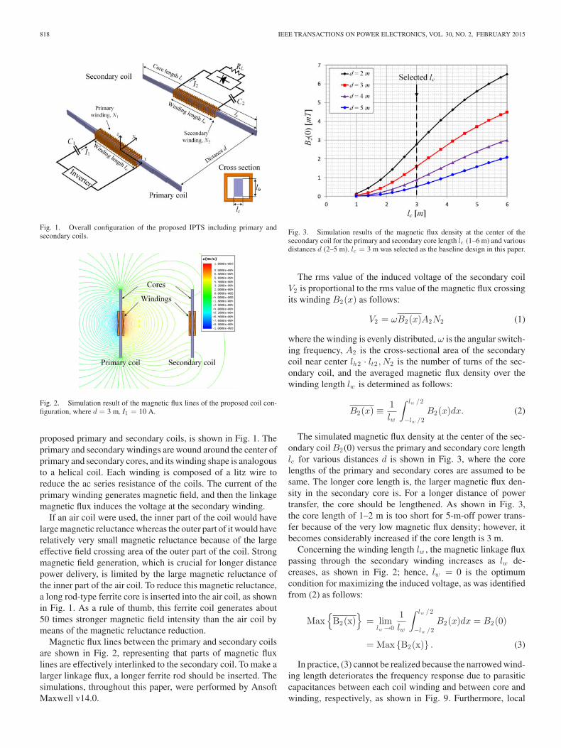
Fig. 12. Circuit diagram of the proposed IPTS for experiments, which includesan inverter for the primary coil driving and a rectifier for the secondary coil.
TABLE IIPARAMETERS OF THE PROPOSED IPTS INCLUDING COILS
These are summarized as follows:
ω ∼= 1.05 ω1 =1.05√L1C1
(27a)
ω = ω2 =1√
L2C2. (27b)
From (27), C1 and C2 were determined by using the measuredvalues of L1 and L2 , which are listed in Table II.
A full bridge rectifier converts the induced ac voltage of thesecondary coil to dc voltage. The R1 and R2 represent primaryand secondary effective series ac resistances, respectively, whichinclude the equivalent series resistances (ESR) of the resonantcapacitors and equivalent ac resistances of the coils compriseof conduction loss and eddy current loss. RL was fixed to 40 Ωthroughout the experiments to give 1 kW at 200-V load voltage.
B. Fabrication of Coils
The proposed coils designed in the previous sections werefabricated, as shown in Figs. 9 and 11, which are the stepped core
Fig. 13. Measured output power versus the primary rms current I1 for variousdistances. (20 kHz).
type and even core type. The lengths of primary and secondarycores are all lc = 3 m, and other parameters for fabricationare listed in Table II. For fabrication, we selected a low-pricedMn–Zn type soft ferrite material named PL-7 from SamwhaElectronics, Korea because the material’s loss characteristic issimilar to a Mn–Zn type material called 3C30 produced byFerrox Cube.
The primary coil inductance L1 was measured as 832 μH,which is 12% less than the simulated value of 942 μH; this ismainly due to thin isolation films between each ferrite block,which were inserted to mitigate eddy current loss inside thecores.
The acryl spacers were also inserted between the wire andferrite core to reduce Cf in order to obtain about a 3 cm gap.Thus, the measured parasitic capacitances of the primary andsecondary coils, Cp1 and Cp2 , were merely 95 and 44 pF, re-spectively. Comparing these values of Cp1 and Cp2 with C1= 80 nF and C2 = 7.1 nF, they are 0.12% and 0.62%, whichcorrespond to 28.9 and 12.7 times frequency separation of (26),respectively. In other words, the parallel resonance frequenciesof the primary and secondary coils are 566 and 256 kHz, re-spectively; hence, the fabricated coils can be used up to about ahundred kilohertz in practice.
C. Efficiency Measurements
To measure the power efficiency of the proposed IPTS, theac input power of the primary coil was measured by a precisiondigital power analyzer, Yokogawa, WT1800, whereas the dcoutput power of the load resistor was measured by multimeters.The measured output power versus the primary current I1 forvarious distances at 20 kHz is shown in Fig. 13. The maximumoutput powers for distances 3, 4, and 5 m were 1403, 471,and 209 W at the maximum primary current I1 = 47 Arms ,respectively.
Fig. 14(a) shows the power efficiency measured from the pri-mary coil to the load resistor versus the output power PL forvarious distances d. The maximum output powers and efficien-cies for 3, 4, and 5 m at 20 kHz were 1403, 471, 209 W, and29%, 16%, 8%, respectively. The power efficiency decreases as
824 IEEE TRANSACTIONS ON POWER ELECTRONICS, VOL. 30, NO. 2, FEBRUARY 2015
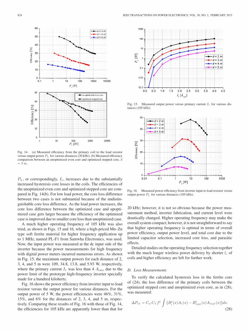
Fig. 14. (a) Measured efficiency from the primary coil to the load resistorversus output power PL for various distances (20 kHz). (b) Measured efficiencycomparison between an unoptimized even core and optimized stepped core, d= 3 m.
PL , or correspondingly, I1 , increases due to the substantiallyincreased hysteresis core losses in the coils. The efficiencies ofthe unoptimized even core and optimized stepped core are com-pared in Fig. 14(b). For low load power, the core loss differencebetween two cases is not substantial because of the undistin-guishable core loss difference. As the load power increases, thecore loss difference between the optimized case and upopti-mized case gets larger because the efficiency of the optimizedcase is improved due to smaller core loss than unoptimized case.
A much higher operating frequency of 105 kHz was alsotried, as shown in Figs. 15 and 16, where a high-priced Mn–Zntype soft ferrite material for higher frequency application upto 1 MHz, named PL-F1 from Samwha Electronics, was used.Now, the input power was measured at the dc input side of theinverter because the power measurements for high frequencywith digital power meters incurred numerous errors. As shownin Fig. 15, the maximum output powers for each distance of 2,3, 4, and 5 m were 109, 34.8, 13.8, and 5.93 W, respectively,where the primary current I1 was less than 4 Arms due to thepower limit of the prototype high-frequency inverter speciallymade for a hundred kilohertz.
Fig. 16 shows the power efficiency from inverter input to loadresistor versus the output power for various distances. For theoutput power of 5 W, the power efficiencies were 46%, 31%,15%, and 6% for the distances of 2, 3, 4, and 5 m, respec-tively. Comparing these results of Fig. 16 with those of Fig. 14,the efficiencies for 105 kHz are apparently lower than that for
Fig. 15. Measured output power versus primary current I1 for various dis-tances (105 kHz).
Fig. 16. Measured power efficiency from inverter input to load resistor versusoutput power PL for various distances (105 kHz).
20 kHz; however, it is not so obvious because the power mea-surement method, inverter fabrication, and current level weredrastically changed. Higher operating frequency may make theoverall system compact; however, it is not straightforward to saythat higher operating frequency is optimal in terms of overallpower efficiency, output power level, and total cost due to thelimited capacitor selection, increased core loss, and parasiticeffects.
Detailed studies on the operating frequency selection togetherwith the much longer wireless power delivery by shorter lc ofcoils and higher efficiency are left for further work.
D. Loss Measurements
To verify the calculated hysteresis loss in the ferrite coreof (24), the loss difference of the primary coils between theoptimized stepped core and unoptimized even core, as in (28),was measured:
ΔP1h = Cm CT fp
∫{Bq
1(x)A1 (x) − Bq
1opt (x)A1opt (x)}dx.
(28)
PARK et al.: INNOVATIVE 5-M-OFF-DISTANCE INDUCTIVE POWER TRANSFER SYSTEMS WITH OPTIMALLY SHAPED DIPOLE COILS 825
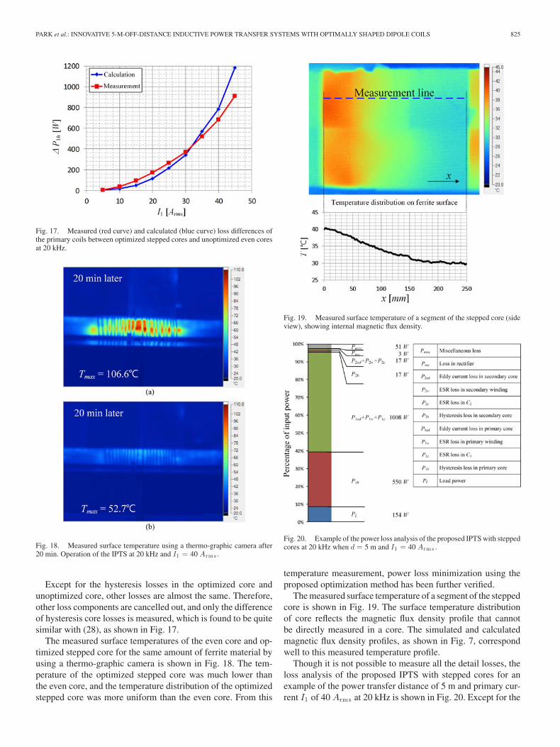
Fig. 17. Measured (red curve) and calculated (blue curve) loss differences ofthe primary coils between optimized stepped cores and unoptimized even coresat 20 kHz.
Fig. 18. Measured surface temperature using a thermo-graphic camera after20 min. Operation of the IPTS at 20 kHz and I1 = 40 Arm s .
Except for the hysteresis losses in the optimized core andunoptimized core, other losses are almost the same. Therefore,other loss components are cancelled out, and only the differenceof hysteresis core losses is measured, which is found to be quitesimilar with (28), as shown in Fig. 17.
The measured surface temperatures of the even core and op-timized stepped core for the same amount of ferrite material byusing a thermo-graphic camera is shown in Fig. 18. The tem-perature of the optimized stepped core was much lower thanthe even core, and the temperature distribution of the optimizedstepped core was more uniform than the even core. From this
Fig. 19. Measured surface temperature of a segment of the stepped core (sideview), showing internal magnetic flux density.
Fig. 20. Example of the power loss analysis of the proposed IPTS with steppedcores at 20 kHz when d = 5 m and I1 = 40 Arm s .
temperature measurement, power loss minimization using theproposed optimization method has been further verified.
The measured surface temperature of a segment of the steppedcore is shown in Fig. 19. The surface temperature distributionof core reflects the magnetic flux density profile that cannotbe directly measured in a core. The simulated and calculatedmagnetic flux density profiles, as shown in Fig. 7, correspondwell to this measured temperature profile.
Though it is not possible to measure all the detail losses, theloss analysis of the proposed IPTS with stepped cores for anexample of the power transfer distance of 5 m and primary cur-rent I1 of 40 Arms at 20 kHz is shown in Fig. 20. Except for the

826 IEEE TRANSACTIONS ON POWER ELECTRONICS, VOL. 30, NO. 2, FEBRUARY 2015
term Pmisc which is the remaining unexplained discrepancy, thepowers were either measured or calculated; P1h and P2h werecalculated from (24) and all the other powers were measured.The dominant losses are found to be the hysteresis and eddy cur-rent losses of the primary coil. Therefore, better a ferrite coreshould be developed for a long distance wireless power transferwith higher system efficiency.
The parameters of the proposed IPTS are summarized inTable II. The effective ac resistances R1 and R2 were measuredby tuning the resonant circuits of the primary and secondarycoils at the operating frequency of 20 kHz, respectively. Themutual inductance Lm was calculated from the measured in-duced voltage V2 for a given primary current I1 . The mutuallycoupling factor κ was calculated from Lm ,L1 , and L2 .
Note that the quality factor of the secondary circuit Q2 for20 kHz, considering the effective ac side resistance of dc sideresistor [31], is merely 30.2 as follows:
Q2 ≡ ωL2
Re=
ωL2
RL,eff + R2=
ωL2
RL8
π 2 + R2, RL,eff
=
(2√
2π
)2
RL. (29)
Comparing the very large Q of the CMRS, the proposed Q2is about 100 times smaller; hence, the proposed IPTS is wellwithin the practical Q2 of less than 100, which has been verifiedby several applications [11], [32], [33].
IV. CONCLUSION
The 5-m-off-long-distance IPTS has been demonstrated, in-troducing the possibility of a new remote power delivery mech-anism that has never been implemented, even by the CMRS, sofar. The dipole structure coil with a ferrite core instead of con-ventional loop-type coils used in the CMRS is found to be quiteeffective for a longer power delivery. Its shape is not bulky butnarrow and long so that it can be installed in the corner or ceilingof a room. The proposed optimized stepped core has been ex-perimentally verified to have only 41% core loss compared withthe unoptimized even core but delivers 2.1 times more wire-less power for a given amount of core. Experimentally obtainedmaximum output powers and primary-coil-to-load-power effi-ciencies for 3, 4, and 5 m at 20 kHz were 1403, 471, 209 W,and 29%, 16%, 8%, respectively. The proposed IPTS is underdevelopment as a potential back-up power of essential sensorsduring severe accidents in a nuclear power plant.
REFERENCES
[1] N. Tesla, “Apparatus for transmitting electrical energy,” U.S. Patent1 119 732, Dec. 1, 1914.
[2] A. Kurs, A. Karalis, R. Moffatt, J. D. Joannopoulos, P. Fisher, andM. Soljacic, “Wireless power transfer via strongly coupled magnetic res-onances,” Science, vol. 317, no. 5834, pp. 83–86, Jul. 2007.
[3] L. H. Ford, “The effect of humidity on the calibration of precision aircapacitors,” J. Inst. Power Eng., vol. 95, no. 48, pp. 709–712, Dec. 1948.
[4] V. J. Brusamarello, Y. B. Blauth, R. Azambuja, I. Muller, and F. R. Sousa,“Power transfer with an inductive link and wireless tuning,” IEEE Trans.Instrum. Meas., vol. 62, no. 5, pp. 924–931, May 2013.
[5] T. C. Beh, M. Kato, T. Imura, Sehoon Oh, and Y. Hori, “Automatedimpedance matching system for robust wireless power transfer via mag-netic resonance coupling,” IEEE Trans. Ind. Electron., vol. 60, no. 9,pp. 3689–3698, Sep. 2013.
[6] A. P. Sample, D. T. Meyer, and J. R. Smith, “Analysis, experimental re-sults, and range adaptation of magnetically coupled resonators for wirelesspower transfer,” IEEE Trans. Ind. Electron., vol. 58, no. 2, pp. 544–554,Feb. 2010.
[7] Sony Corp. (2009, Oct. 2). Sony develops highly efficient wirelesspower transfer system based on magnetic resonance. [Online]. Available:http://www.sony.net/SonyInfo/News/Press/200910/09-119E/index.html
[8] J. Hirai, T.-W. Kim, and A. Kawamura, “Study on intelligent batterycharging using inductive transmission of power and information,” IEEETrans. Power Electron., vol. 15, no. 2, pp. 335–345, Mar. 2000.
[9] B. L. Cannon, J. F. Hoburg, D. D. Stancil, and S. C. Goldstein, “Magneticresonant coupling as a potential means for wireless power transfer tomultiple small receivers,” IEEE Trans. Power Electron., vol. 24, no. 7,pp. 1819–1825, Jul. 2009.
[10] M. Budhia, G. A. Covic, and J. T. Boys, “Design and optimization ofcircular magnetic structures for lumped inductive power transfer systems,”IEEE Trans. Power Electron., vol. 26, no. 11, pp. 3096–3108, Nov. 2011.
[11] J. Huh, S. W. Lee, W. Y. Lee, G. H. Cho, and C. T. Rim, “Narrow-width in-ductive power transfer system for online electrical vehicles,” IEEE Trans.Power Electron., vol. 26, no. 12, pp. 3666–3679, Dec. 2011.
[12] S. H. Lee and R. D. Lorenz, “Development and validation of model for95%-efficiency 220-W wireless power transfer over a 30-cm Air Gap,”IEEE Trans. Ind. Appl., vol. 47, no. 6, pp. 2495–2504, Nov.-Dec. 2011.
[13] H. Matsumoto, Y. Neba, K. Ishizaka, and R. Itoh, “Comparison of charac-teristics on planar contactless power transfer systems,” IEEE Trans. PowerElectron., vol. 27, no. 6, pp. 2980–2993, Jun. 2012.
[14] Z. Pantic and S. M. Lukic, “Framework and topology for active tuning ofparallel compensated receivers in power transfer systems,” IEEE Trans.Power Electron., vol. 27, no. 11, pp. 4503–4513, Nov. 2012.
[15] J. P. C. Smeets, T. T. Overboom, J. W. Jansen, and E. A. Lomonova,“Comparison of position-independent contactless energy transfer sys-tems,” IEEE Trans. Power Electron., vol. 28, no. 4, pp. 2059–2067, Apr.2013.
[16] M. Pinuela, D. C. Yates, S. Lucyszyn, and P. D. Mitcheson, “MaximizingDC-to-load efficiency for inductive power transfer,” IEEE Trans. PowerElectron., vol. 28, no. 5, pp. 2437–2447, May 2013.
[17] S. Lee, B. Choi, and C. T. Rim, “Dynamics characterization of the induc-tive power transfer system for online electric vehicles by laplace phasortransform,” IEEE Trans. Power Electron., vol. 28, no. 12, pp. 5902–5909,Dec. 2013.
[18] Y. Zhang, Z. Zhao, and K. Chen, “Frequency decrease analysis of resonantwireless power transfer,” IEEE Trans. Power Electron., vol. 29, no. 3,pp. 1058–1063, Mar. 2014.
[19] H. Hao, G. A. Covic, and J. T. Boys, “A parallel topology for inductivepower transfer power supplies,” IEEE Trans. Power Electron., vol. 29,no. 3, pp. 1140–1151, Mar. 2014.
[20] C.-S. Wang, G. A. Covic, and O. H. Stielau, “Power transfer capabilityand bifurcation phenomena of loosely coupled inductive power transfersystems,” IEEE Trans. Ind. Electron., vol. 51, no. 1, pp. 148–157, Feb.2004.
[21] Z. N. Low, R. A. Chinga, R. Tseng, and J. Lin, “Design and test of ahigh-power high-efficiency loosely coupled planar wireless power transfersystem,” IEEE Trans. Ind. Electron., vol. 56, no. 5, pp. 1801–1812, May2009.
[22] J. Sallan, J. L. Villa, A. Llombart, and J. F. Sanz, “Optimal design ofICPT systems applied to electric vehicle battery charge,” IEEE Trans.Ind. Electron., vol. 56, no. 6, pp. 2140–2149, Jun. 2009.
[23] J. U. W. Hsu, A. P. Hu, and A. Swain, “A wireless power pickup basedon directional tuning control of magnetic amplifier,” IEEE Trans. Ind.Electron., vol. 56, no. 7, pp. 2771–2781, Jul. 2009.
[24] G. Elliott, S. Raabe, G. A. Covic, and J. T. Boys, “Multiphase pickups forlarge lateral tolerance contactless power-transfer systems,” IEEE Trans.Ind. Electron., vol. 57, no. 5, pp. 1590–1598, May 2010.
[25] M. L. G. Kissin, G. A. Covic, and J. T. Boys, “Steady-state flat-pickuploading effects in polyphase inductive power transfer systems,” IEEETrans. Ind. Electron., vol. 58, no. 6, pp. 2274–2282, Jun. 2011.
[26] F. F. A. van der Pijl, M. Castilla, and P. Bauer, “Adaptive sliding-modecontrol for a multiple-user inductive power transfer system without needfor communication,” IEEE Trans. Ind. Electron., vol. 60, no. 1, pp. 271–279, Jan. 2013.
PARK et al.: INNOVATIVE 5-M-OFF-DISTANCE INDUCTIVE POWER TRANSFER SYSTEMS WITH OPTIMALLY SHAPED DIPOLE COILS 827
[27] S. Chopra and P. Bauer, “Driving range extension of EV with on-roadcontactless power transfer—A case study,” IEEE Trans. Ind. Electron.,vol. 60, no. 1, pp. 329–338, Jan. 2013.
[28] D. Kurschner, C. Rathge, and U. Jumar, “Design methodology for highefficient inductive power transfer systems with high coil positioning flexi-bility,” IEEE Trans. Ind. Electron., vol. 60, no. 1, pp. 372–381, Jan. 2013.
[29] J. Shin, S. Shin, Y. Kim, S. Ahn, S. Lee, G. Jung, S.-J. Jeon, and D.-H. Cho,“Design and implementation of shaped magnetic-resonance-based wire-less power transfer system for roadway-powered moving electric vehi-cles,” IEEE Trans. Ind. Electron., vol. 61, no. 3, pp. 1179–1192, Mar.2014.
[30] Ferrox Cube. Design of planar power transformers. [Online]. Available:http://www.ferroxcube.com/appl/info/plandesi.pdf
[31] C. T. Rim and G. H. Cho, “Phasor transformation and its application to theDC/AC analyses of frequency/phase controlled series resonant converters(SRC),” IEEE Trans. Power Electron., vol. 5, no. 2, pp. 201–211, Apr.1990.
[32] W. Y. Lee, J. Huh, S. Y. Choi, X. V. Thai, J. H. Kim, E. A. Al-Ammar,M. A. El-Kady, and C. T. Rim, “Finite-width magnetic mirror models ofmono and dual coils for wireless electric vehicles,” IEEE Trans. PowerElectron., vol. 28, no. 3, pp. 1413–1428, Mar. 2013.
[33] S. Choi, J. Huh, S. Lee, and C. T. Rim, “New cross-segmented powersupply rails for roadway powered electric vehicles,” IEEE Trans. PowerElectron., vol. 28, no. 12, pp. 5832–5841, Dec. 2013.
[34] G. A. Covic and J. T. Boys, “Modern trends in inductive power transfer fortransportation applications,” IEEE J. Emerg. Sel. Topics Power Electron.,vol. 1, no. 1, pp. 28–41, Mar. 2013.
[35] C. B. Park, S. W. Lee, and C. T. Rim, “5m-off-long-distance inductivepower transfer system using optimum shaped dipole coils,” in Proc. Int.Power Electron. Motion Control Conf., Jun. 2012, pp. 1137–1142.
Changbyung Park (S’10) received the B.S. and M.Sdegrees in electrical engineering from the Korea Ad-vanced Institute of Science and Technology (KAIST),Daejeon, Korea, in 2008 and 2010, respectively He iscurrently working toward the Ph.D. degree at KAIST.
He has worked on developing an LED driver ICand a column driver IC for LCD, and wireless powertransfer system. His current research interests includewireless power transfer system and touch read-outcircuit.
Sungwoo Lee received the B.S. degree from KoreaUniversity, Seoul, Korea, in 2007, and the IntegratedMaster’s Ph.D. degree in electrical engineering fromthe Korea Advanced Institute of Science and Tech-nology (KAIST), Daejeon, Korea.
He has been working at Samsung electronics,Yong-In, Korea. His research interests are in the fieldof analog integrated circuit design, and his currentresearch interests include the power management ICand in the contactless power supply.
Gyu-Hyeong Cho (S’76–M’80–SM’11) was born inKorea in 1953. He received the B.S. degree fromHanyang University, Seoul, Korea, and the M.S. andPh.D. degrees in electrical engineering from the Ko-rea Advanced Institute of Science and Technology(KAIST), Daejeon, Korea, in 1975, 1977, and 1981,respectively.
From 1982 to 1983, he was with the Westing-house R&D Center, Pittsburgh, PA, USA, and joinedthe Department of Electrical Engineering, KAIST, in1984. He has been a Tenured Professor since 1991
and was a Visiting Professor at the University of Wisconsin, Madison, in 1989.He performed research in the area of power electronics until the late 1990sand has worked on soft-switching converters, high-power and high-voltage in-verters, and static VAR compensators; he later shifted to researching analogintegrated circuit designs. His recent research focuses on two areas. One is thecombined area of analog integrated circuits and power electronics, includingsmart power ICs, such as single-chip power management ICs and Class D audiopower amplifiers. The other area is display driver ICs for LED, OLED, and LCDflat panel displays.
Chun T. Rim (M’90–SM’11) was born in Korea in1963. He received the B.S. degree in electrical engi-neering from the Kumoh National Institute of Tech-nology, Gumi-si, Korea, in 1985, and the M.S. andPh.D. degrees in electrical engineering from the Ko-rea Advanced Institute of Technology (KAIST), Dae-jeon, Korea, in 1987 and 1990, respectively.
Since 2007, he has been an Associate Professor ofNuclear and Quantum Engineering, and an adjunctto Aerospace Engineering in Power Electronics atKAIST. He is currently developing inductive power
transfer systems for On-Line Electrical Vehicles and leading the Nuclear PowerElectronics and Robots Lab, named the Tesla Lab, at KAIST. From 1990 to 1995,he was a Military Officer at the Ministry of National Defense in Korea. From1995 to 2003, he was a Senior Researcher at the Agency for Defense Devel-opment, Daejeon, and from 1997 to 1999, he was with Astrium in Portsmouth,U.K. From 2003 to 2007, he was a Senior Director at the Presidential Office,Seoul, Korea. He was involved in developing Korea’s first airborne and space-borne Synthetic Aperture Radars. His research interests include wireless electricvehicles, wireless power systems for robots and bio-medical applications, andenergy grid applications. He has authored or coauthored 81 technical papers,written four books, and holds more than 99 patents (awarded and pending).
Dr. Rim has received three prizes from the Korean government.