Embed Size (px)
Citation preview

Influence of pick & place
machines on product quality
The impact of placement quality on SMT manufacturing costs

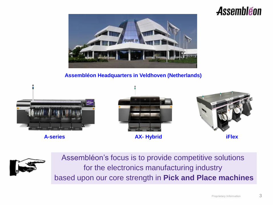
ABOUT ASSEMBLEON
Introduction
3
Assembléon Headquarters in Veldhoven (Netherlands)
Assembléon’s focus is to provide competitive solutions
for the electronics manufacturing industry
based upon our core strength in Pick and Place machines
A-series AX- Hybrid iFlex

SMT PROCESS Q CRITERIA
SMT process quality influencing factors
4

5
Typical SMT process flow
Solder paste
printingComponent placement Reflow soldering

6
SMT process requirements
Solder paste
printingComponent placement Reflow soldering
• Right amount
• Right place
• Right component
• Right place
• Right temperature profile
• Good reflow
Process requirements

7
Assessment criteria for stencil printing process
1. Solder paste pattern resolution (paste transfer)
2. Bridging (‘smearing’)
3. Misalignment
Stencil printing

8
0 no paste
1 irregular shape (few balls)
2 pyramid lower than stencil
thickness
3 pyramid equal to stencil thickness
4 beginning flat top with "dog ears"
5 flat top side
6 scooped-out
0 1 2 3 4 5 6
Solder paste pattern resolution
OK !
Stencil printing

9
OK !
Solder paste smearing
Criterion:
Neighboring pads
May not have contact
Flux with incidental balls
Perfect
Smearing
Stencil printing

10
Solder paste pattern misalignment
Perfect Acceptable Not acceptable
100% of paste
centered on pad
< 25% of paste
off-pad
> 25% of paste
off-pad
Acceptable Acceptable Not acceptable
100% of paste
on pad
< 25% of paste
off-pad
> 25% of paste
off-pad
Remedy:
Board to stencil
alignment correction
Stencil printing

11
Placement defect analysis
Symptom
(before reflow)
Cause Defect
(end of process)
Part misaligned
Incorrect part
Part damaged
Wrong polarity
Extra / missing part
• Mis read fiducials
• Machine needs calibration
• Placement error
• Alignment error
• Part slid off pads
• Incorrect part reel loading
• Tape splice error
• Part damaged at supplier
• Placement force too high
• Programming error
• Tray rotated
• Part lost during pick & place
• Misalignment
• Solder bridging
• Tombstoning
•Incorrect part
• Opens
• Component cracking
• Tilted part
• Wrong polarity
• Extra / missing part
Pick & place

12
Reflow solder process requirements
240 - 280 deg. C
205 deg. C180 deg. C160 deg. C
Temperature
Time< 70 sec< 60 sec
Pre-heat
Soack
ReflowMinimum soldering temperature
Maximum soldering temperature
235 deg. CReflow zone for Lead-free
Reflow zone for PbSn217 deg. C
< 70 sec
Soak
< 3C / sec < 6C / sec
Reflow soldering

13
Reflow process defect analysisPeak temperature too high:
• Charring
• Delamination
• Intermetallics
• Leaching
• Dewetting
• Voiding
Cooling rate too fast
• Solder detachment
• Pad Detachment
Cooling rate too slow
• Intermetalllics
• Charring
• Leaching
• Dewetting
• Grain Size too large
Soaking Zone too long
• Voiding
• Poor Wetting
• Solder Balling
• Opens
Ramp-up rate too high
• Hot Slump
• Bridging
• Tombstoning
• Skewing
• Wicking
• Opens
• Solder beading
• Solder balling
• Components cracking.
Reflow soldering

14
Acceptable part to pad misalignment (IPC-A-610D)
Before reflow After reflow
Self alignment: solder to pad
Self alignment: part to solder
Reflow soldering

PICK & PLACE RELATED ERRORS
Relationship placement machine concept and placement quality control
15

16
Possible defects in SMT: defect opportunities
1. Component opportunities (OC)
All parts that need to be assembled on board (incl. PCB)
Every part counts for one defect opportunity
Defect example: damaged parts
2. Placement opportunity (OP)
All parts that need to be placed on board, based on bill of materials (excl. PCB)
Every part counts for one defect opportunity
Defect examples: misaligned parts, missing parts
3. Termination opportunity (OT)
Any hole, pad or land or other surface to which a component is electrically
terminated
Every termination counts for one defect opportunity
(example: QFP48 48 leads 48 termination opportunities)
4. Assembly opportunity (OA)
An overall defect opportunity that is not captured within component, placement or
termination opportunity defect classes
Defect examples: conformal coating, cleaning
17
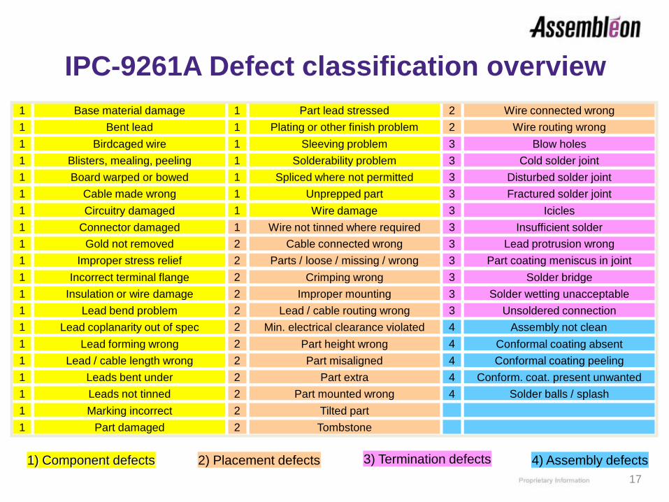
IPC-9261A Defect classification overview
Base material damage
Bent lead
Birdcaged wire
Blisters, mealing, peeling
Board warped or bowed
Cable made wrong
Circuitry damaged
Connector damaged
Gold not removed
Improper stress relief
Incorrect terminal flange
Insulation or wire damage
Lead bend problem
Lead coplanarity out of spec
Lead forming wrong
Lead / cable length wrong
Leads bent under
Leads not tinned
Marking incorrect
Part damaged
1
1
1
1
1
1
1
1
1
1
1
1
1
1
1
1
1
1
1
1
Part lead stressed
Plating or other finish problem
Sleeving problem
Solderability problem
Spliced where not permitted
Unprepped part
Wire damage
Wire not tinned where required
Cable connected wrong
Parts / loose / missing / wrong
Crimping wrong
Improper mounting
Lead / cable routing wrong
Min. electrical clearance violated
Part height wrong
Part misaligned
Part extra
Part mounted wrong
Tilted part
Tombstone
1
1
1
1
1
1
1
1
2
2
2
2
2
2
2
2
2
2
2
2
Wire connected wrong
Wire routing wrong
Blow holes
Cold solder joint
Disturbed solder joint
Fractured solder joint
Icicles
Insufficient solder
Lead protrusion wrong
Part coating meniscus in joint
Solder bridge
Solder wetting unacceptable
Unsoldered connection
Assembly not clean
Conformal coating absent
Conformal coating peeling
Conform. coat. present unwanted
Solder balls / splash
2
2
3
3
3
3
3
3
3
3
3
3
3
4
4
4
4
4
1) Component defects 2) Placement defects 3) Termination defects 4) Assembly defects

18
Yield vs. number of defect opportunities
0.00
0.20
0.40
0.60
0.80
1.00
1.20
0 5000 10000 15000 20000 25000 30000 35000 40000
Defect opportunities
Es
tim
ate
d Y
ield
5 10 20 30 40 50 75 100 150 200 300 400 500 750 1000DPMO =
Lower DPMO will increase Yield and thus reduce repair costs
Mobile phone application 2012

19
Most pick & place machines are sequential
• High accelerations / decelerations
High forces acting on components risk of component shift or loss
• No component position monitoring between component alignment
and placement position
• In most cases: no placement force control / no presence check
PLACEMENT HEAD
Pick Place

20
Acceleration forces acting on pipettes
Hg
m.g [N]
a [m/s2]m.a [N]
Di
Do
Ffriction
Risk of components shift:
Acceleration force (= m.a) > friction force
Risk of components break loose:
m.a.Hg > Fvacuum.(Do/2)
Revolver & turret heads add extra acceleration forces

21
Parallel pick & place principle
• Multiple parallel placement robots
• Indexing board transport
• Single placement head per robot
COMPONENT SUPPLY
PCBs
PICK
TRANSFER
PLACE
PLACEMENT HEAD

22
Total pick & place process control
Pick
Place
Pick height control Component presence check
Component inspection
Component alignment
On-edge detection
Component
force
control
Component presence check
Component presence check
Component
pick
correction

23
Placement head with integrated P&P process feedback
Phi-Z module
BA-camera module
Laser Align module
PCBAuto calibration
Short accuracy loops
Component pick correction

24
Force control
Impact force is determined by :
• Velocity
• High velocity high impact force
• Contact stiffness
• High stiffness high impact force
• Impact mass
• High mass high impact force
Placement head
PCB
Contact stiffness
staticimpactplacement FFF
contactimpact kmvF
No force control:
Risk of component cracking

Impact
detection
Impact force control
25
height
force
Static force
PCB / Substrate

26
Placement defect prevention
Symptom
(before reflow)
Cause Defect
(end of process)
Part misaligned
Incorrect part
Part damaged
Wrong polarity
Extra / missing part
• Mis read fiducials
• Machine needs calibration
• Placement error
• Alignment error
• Part slid off pads
• Incorrect part reel loading
• Tape splice error
• Part damaged at supplier
• Placement force too high
• Programming error
• Tray rotated
• Part lost during pick & place
• Misalignment
• Solder bridging
• Tombstoning
• Incorrect part
• Opens
• Component cracking
• Tilted part
• Wrong polarity
• Extra / missing part
Auto calibration
Short accuracy
loops
Low accelerations
Servo Z movement
On edge detection
Pick correction
Setup verification
Splice detection
Force control
Presence check
Pick & place

RESULTS
Relationship DPMO and rework costs
27

28
DPMO results for parallel placement
machines
Product: LCD television (Shenzhen, China) (790 parts / board)
Line A: Parallel placement
DPUtotal (5 days) = 0.0399 Y = 96.1%
Line B: Sequential placement
DPUtotal (5 days) = 0.2873 Y = 75%
WORK MONTH 08-30 08-31 09-01 09-02 09-03
INSPECTION(output) 1030 2332 2940 2850 2136
PASS 993 2302 2919 2801 2136
FAILED 37 30 21 49
TOTAL DEFECT 112 96 49 142 52
DPU 0.109 0.041 0.017 0.050 0.024
DPMO
DPU control level 0.094 0.094 0.094 0.094 0.094
DPMO control level
DEFECT BREAKDOWN QTY QTY QTY QTY QTY
COMPONENT RELATED
Bend lead
PROCESS RELATED DEFECT
Wrong Direction
Wrong Component
Missing Component 1 1 7 6 6
Extra Component 3 2 1
Damaged Component
Misalignment 4 5 5
Tombstone 10 16 17 9
Component reversal 1 4
Component incline
Component high
total defect 11 24 10 33 20
DPM 14 13 4 15 12
WORK MONTH 08-28 08-29 08-30 09-01 09-02
INSPECTION(output) 628 104 420 120 1610
PASS 612 92 394 110 1574
FAILED 16 12 26 10 36
TOTAL DEFECT 126 221 147 190 144
DPU 0.201 2.121 0.349 1.584 0.090
DPMO
DPU control level 0.094 0.094 0.094 0.094 0.094
DPMO control level
DEFECT BREAKDOWN QTY QTY QTY QTY QTY
COMPONENT RELATED
Bend lead
PROCESS RELATED DEFECT
Wrong Direction
Wrong Component
Missing Component 24 2 6 9 16
Extra Component 1
Damaged Component
Misalignment 6 11 3
Tombstone 1 12 10 5 29
Component reversal
Component incline
Component high
total defect 31 14 27 14 49
DPM 64 193 87 161 39
Difference in first pass yield: 21.1%

29
Example: Rework cost savings for LCD television
Item Parallel line Sequential line
# Productive hours per year 7800 7800
Real output per line [cph] 100000 100000
# Components per board 790 790
# Defect opportunities per board 5700 5700
DPMO 7 50
DPU 0.04 0.29
First pass yield [%] 96% 75%
Average BOM cost per part [€] 0.07 0.07
Line cycle time [s] 28.44 28.44
# Repairs per hour (board level) 5 31
Average rework per hour [s] 2674 16951
# Rework operators (3 shifts) 2 14
Annual labor cost per operator [k€] 3 3
Total annual labor cost [k€] 7 45
# Rework stations needed 1 5
Annual station costs (excl. labor) [k€] 20 100
Annual BOM rework costs [k€] 3 17
Total repairs per line per year [-] 38619 244847
Total repair costs per line (per year) [k€] 30 162
Average defect coverage [%] 90.00 90.00
# Boards needing second order rework (per year) 3862 24485
Average second order rework per hour [s] 267 1695
# Rework operators (3 shifts) 0 2
Total annual labor cost [k€] 1 5
# Rework stations needed 1 1
Annual station costs (excl. labor) [k€] 20 20
Annual BOM rework costs [k€] 0.26 1.66
Second order repair costs (per year) [k€] 21.2 26.5
Total repair costs per line
(incl. defect recov. per year) [k€]51.2 188.6

30
Quality inspection methods
AXI
Automatic X-ray Inspection
ICT
In-Circuit Test
AOI
Automatic Optical Inspection

31
Defect coverage estimates
Source: Nokia & University of Oulu, Finland, 2005
HVI: Human Visual Inspection
ICT: In Circuit Testing
AOI: Automatic Optical Inspection
AXI: Automatic X-ray Inspection
BSCAN: Boundary Scan
A combination of different test methods is needed for optimal test coverage
Approximate test coverage: 90% ( 10% of all defects is not detected)

32
Conclusion
• Prevention is better than cure…
Solder paste printing
• Selection of optimal stencil & aperture definition
• Selection of optimal printing parameters
• Process monitoring (stencil cleaning, paste replenishment, etc.)
Component placement
• Monitoring of every pick & place process step
• Selection of optimal P&P parameters (‘Take it easy’)
Reflow soldering
• Selection of optimal reflow temperature profile
• Reflow process control
• Parallel placement principle gives intrinsically better placement quality
Continuous process monitoring
More time available per process step less risks
Result: Typical DPMO ≤ 10 Considerable savings on rework cost !

Sjef van Gastel
October 3rd 2012


![Essentials Fabrication Quality Plan Samplefirsttimequalityplans.com/.../03/1049_Essentials-Steel-fabrication... · Pat [Pick the date] Essentials Fabrication Quality Plan Sample](https://img.dokumen.tips/doc/110x75/5a7a0fc17f8b9adf778c6330/essentials-fabrication-quality-plan-samplef-pick-the-date-essentials-fabrication.jpg)