Embed Size (px)
Citation preview

1
INFLUENCE OF GROWTH CONDITIONS
ON THE STRUCTURAL AND ELECTRICAL PROPERTIES
OF GALLIUM ARSENIDE THIN FILMS
I. Hamidah1,2), N. Yuningsih3), P. Arifin1), M. Budiman1), and M. Barmawi1)
1)Lab. For Electronic Materials Physics, Dept. of Physics , Bandung Institut of Technology, Jl. Ganesha No. 10 Bandung 40132
2)Lab. Of Physics, Dept. of Mechanical Engineering, Indonesia University of Education, Jl. Setiabudhi No. 207, Bandung 40154
3)Lab. Of Physics, UP-MKU, Politeknik Negeri Bandung, Jl. Geger kalong Hilir PO Box 6468 BDCD, Bandung 40162
Abstract GaAs films were usually grown by MOCVD using AsH3 and TMGa as precursors. In this study, TDMAAs and TMGa had been successfully used as As and Ga precursor, respectively. For these experiments, the growth temperature was allowed to range from 580 to 600oC, the total reactor pressure was varied from 50 to 70 torr, and the flows of hydrogen and nitrogen were varied from 200 to 400 sccm. The TDMAAs/TMGa ratio was kept at 4.5. The structural and electrical properties are characterized using SEM method and standard van-der Pauw Hall measurement, respectively. The optimum growth condition occurred at growth temperature of 580 oC, reactor pressure of 50 torr, H2/N2 ratio of 1,and V/III ratio of 4.5. This film had grain size of 1.08 µm, growth rate of 0.94 µm/h, 395 cm2/Vs mobility, and hole concentration of 3.44 x 1015 cm-3. Abstrak Film tipis GaAs biasanya ditumbuhkan dengan metoda MOCVD dengan menggunakan precursor AsH3 dan TMGa. Dalam studi ini, TDMAAs dan TMGa telah berhasil digunakan sebagai precursor As dan Ga. Dalam eksperimen ini , parameter penumbuhan diatur sebagai berikut: temperatur penumbuhan divariasikan dari 580 sampai 600 oC, tekanan total dalam reaktor divariasikan dari 50 sampai 70 torr, dan laju aliran H2 dan N2 divariasikan dari 200 sampai 400 sccm, sedangkan perbandingan TDMAAs /TMGa dijaga pada nilai 4,5. Sifat-sifat struktural dan listrik dikarakterisasi dengan menggunakan metoda SEM dan Hall-van der Pauw effect. Kondisi optimum penumbuhan GaAs terjadi pada temperatur penumbuhan 580 oC, tekanan reaktor 50 torr, perbandingan H2/N2 sama dengan 1, dan perbandingan V/III 4,5. Film tersebut memiliki ukuran butir kristal 1,08 µm, laju penumbuhan 0,94 µm/jam, mobilitas 395 cm2/Vs, dan konsentrasi hole 3.44 x 1015 cm-3.
I. INTRODUCTION
In the last few years the interest in Gallium Arsenide (GaAs) rapidly increased because
of their unique electrical and optical properties and the resulting wide range of electronic
applications [1-5]. GaAs-based optoelectronic for optical fiber communications is an
interesting alternative for some important applications such as optical interconnections, fast
switching systems, etc. Beside that, semi-insulating GaAs has received great deal attention
because of its high performance as a substrate for advanced integrated circuits (ICs).

2
Therefore, the state of the art of GaAs growth allows one to obtain a semi-insulating
material without intentional doping. Successful homoepitaxial growth of high purity,
unintentionally doped GaAs layers using metal organic chemical vapor deposition
(MOCVD) has traditionally involved the use of arsine (AsH3) and trimethyl-gallium
(TMGa) as precursors. Unfortunately, the high toxicity of AsH3, which is caused by As-H
bonds, and its inefficient reaction with TMGa [6], as well as the incorporation of carbon
impurities from the TMGa into the layers, are inherent drawbacks to this system. To
overcome those problems, trisdimethylamino-arsenic (TDMAAs) has been proposed as
another alternative precursor with no As-H bonds and As-C bonds [7-9]. In this study,
some phenomena will be reported. These are structural and electrical properties of GaAs
films, which are influenced by growth conditions. The phenomenon is studied by scanning
electron microscopy (SEM) method and the standard Hall-van der Pauw effect
measurement.
II. EXPERIMENT
GaAs films were grown in vertical MOCVD reactor on semi-insulating (100) GaAs
substrate, using TMGa and TDMAAs as Ga and As precursors, respectively. The TMGA
and TDMAAs were introduced to the reactor by carrier gas H2 which is purified in
hydrogen purifier (Palladium diffuser RSI-10). It was assumed that the carrier gas is fully
saturated and the precursor exerted its equilibrium vapor pressure. Thus, the flow rate of the
precursor could be accurately controlled by mass flow controller (MFC) upstream from the
bubbler. For these experiments, the growth temperature was allowed to range from 580 to
600oC, the total reactor pressures were varied from 50 to 70 torr, and the flow of hydrogen
and nitrogen (N2) were varied from 200 to 400 sccm. The TDMAAs/TMGa ratio was kept

3
at 4.5 due to the optimum growth condition, which has been reported in our previous paper
[10]. Growth conditions of GaAs films are presented in table 1. The shadow part shows the
variety of growth conditions.
Table 1. Growth conditions and grain size of GaAs films
V/III Tg (oC) H2/N2 Pg (torr) Grain Size (µm) 4
4.5 5
580 580 580
1 1 1
50 50 50
1.67 1.08 0.78
4.5 4.5 4.5
580 590 600
1 1 1
50 50 50
1.08 3.20 1.84
4.5 4.5 4.5
580 580 580
0.5 1 2
50 50 50
1.8 1.08 0.75
4.5 4.5 4.5
580 580 580
1 1 1
50 60 70
1.08 2.50 1.00
All GaAs films were characterized structurally by SEM method to study the GaAs surface
morphology. The electrical properties of GaAs films were characterized by the standard
Hall-van der Pauw effect measurement at room temperature. Au was deposited on the GaAs
films by evaporation method acting as an Ohmic contact [11-12].
III. RESULT AND DISCUSSION
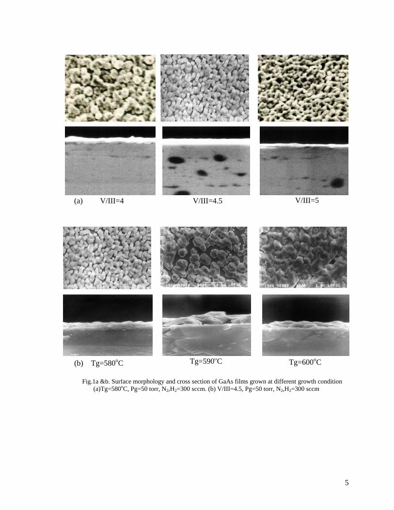
The surface morphology of GaAs films, grown at different growth conditions was
presented in fig. 1. It can be seen that the quality of films are influenced by the V/III ratio,
the growth temperature, the H2/N2 ratio, and the reactor pressure. (a) GaAs films with 4.5
V/III ratio has homogeneous surface morphology, and it has migration between its grain. It
also revealed that the higher V/III ratio, the small the grain size of GaAs . (b) Due to the
goal obtained from (a), GaAs films grown at different growth temperature. It is found that

4
the GaAs are grown at temperatures of 590 and 600oC have grain size larger than 580oC.
But those GaAs have no migration between its grains. So, we can not get information that
of grown at these conditions. (c) We set growth condition by varying total reactor pressure.
GaAs film grown at reactor pressure of 70 torr, has grain that more dense but
inhomogeneous, whereas GaAs film grown at pressure reactor of 60 torr, has no migration
between its grain. (d) GaAs films grown at varying H2/N2 ratio. It is found that the
optimum condition for obtaining GaAs film with good morphology is by using H2/N2 ratio
of 1. That film has grain size bigger than the other and more homogeneous (d). The effect
of growth conditions on the grain size is presented in table 1.
The growth rates of all films vary from 0.4 to 1.25 µm/h. The fastest growth rate is
obtained for GaAs film grown at V/III ratio of 4.5, growth temperature of 590oC, reactor
pressure of 50 torr, and H2/N2 ratio of 1. However, from the fig. 1, it can be seen that, this
film has no migration between its grain. For this condition, cohesive energy between atoms
of films is stronger than cohesive energy between atoms of films and atoms of substrate, so
island growth is formed [13].
The result obtained from electrical measurement of GaAs films, are summarized in
fig.3. All of films have p-type conductivity. The room temperature mobility and the hole
concentration exhibit growth temperature and V/III ratio dependency [14]. GaAs films with
4 and 5 V/III ratios and 590 and 600 oC growth temperatures have low mobility. It is
caused by the absence of migration between its grain, as can be seen from fig. 1. Mobility
for GaAs film with 4.5 V/III ratio and 580 oC growth temperature has high mobility, i.e.
395 cm2/Vs. These results are comparable to those obtained by Dong [9].
5
Fig.1a &b. Surface morphology and cross section of GaAs films grown at different growth condition (a)Tg=580oC, Pg=50 torr, N2,H2=300 sccm. (b) V/III=4.5, Pg=50 torr, N2,H2=300 sccm
(b) Tg=580oC Tg=590oC Tg=600oC
(a) V/III=4 V/III=4.5 V/III=5

6
Fig.1c & d. Surface morphology and cross section of GaAs films grown at different growth condition (c) Tg=580oC, V/III=4.5, N2,H2=300 sccm, (d) Tg=580oC, Pg=50 torr, V/III=4.5.
(d) H2/N2=0.5 H2/N2=1 H2/N2=2
( c ) Pg=50 torr Pg=60 torr Pg=70 torr

7
Fig. 2. Hole concentration (dash line) and mobility (thick line) of GaAs films
The carrier concentration is in the range between 1015 to 1017 cm-3. From fig. 2, we can
see that the higher mobility the lower hole concentration.
IV. CONCLUSION
GaAs films have been successfully grown by MOCVD using TDMAAs and TMGa
precursors. The structural and electrical properties are characterized using SEM method and
standard van-der Pauw Hall measurement, respectively. All the grown films show p-type
conductivity. The optimum growth condition occurs at V/III ratio of 4.5, growth
temperature of 580 oC, H2/N2 ratio of 1 and pressure of reactor of 50 torr. This film has
grain size of 1.08 µm, growth rate of 0.94 µm/h, 395 cm2/Vs mobility, and hole
concentration of 3.44 x 1015 cm-3.
REFERENCES
[1] F.W. Smith, A.R. Calawa, C.L. Chen, M.J. Mantra, L.J. Mahoney, IEEE Electron Device Lett. 9, 77 (1988).
[2] M. Kaminska, Z. Liliental-Weber, E.R. Weber, T. George, J.B. kortright, F.W. Smith, B.Y.Tsaur, and A.R Calawa, Appl. Phys. Lett. 54, 1831 (1989).
[3] M.R. Melloch, K. Mahalingam, N. Otsuka, J.M. Woodall, and, A.C. Warren, J. Cryst. Growth 111, 39 (1991).
[4] N.A. Bert, A.I. Veinger, M.D. Vilisova, S.I. Goloshchapov, I.V. Ivonin, S.V. Kozyrev, A.E. Kunitsyn, L.G. Lavrentieva, D.I. Lubysev,V.V. Preobazhenskii, B.R. Semyagin, V.V. Tretyakov, V.V. Chaldysev, and M.P. Yakubenya, Phys. Solid State 35, 1289 (1993).
0
100
200
300
400
500
3.5 4 4.5 5 5.5
V/III ratio
mob
ility
(cm
2 /Vs)
1.E+14
1.E+15
1.E+16
1.E+17
1.E+18
1.E+19
hole
con
cent
ratio
n (c
m-3
)
0
100
200
300
400
500
570 580 590 600 610
Growth temperature (oC)
mob
ility
(cm
2 /Vs)
1.E+14
1.E+15
1.E+16
1.E+17
1.E+18
hole
con
cent
ratio
n (c
m-3
)

8
[5] J.K. Luo, H. Thomas, D.V. Morgan, D. Westwood, and R.H. Williams, Semicond. Sci. Technol. 9, 2199 (1994).
[6] P.D. Dapkus, H.M. Manasevit, K.L. Hess, T.S. Low, and G.E. Stillman, J. Cryst. Growth 55, 10 (1981).
[7] G. Zimmerman, H.Portmann, T. Marschner, O. Zseboek, W. Stolz, E.O. Goebel, P. Gimnich, J. Loberth, T. Filz, P. Kurpas, and W. Richter, J. Cryst. Growth 129, 37 (1993).
[8] M.H. Zimmer, R. Hovel, W. Brysch, A. Brauers, and P. Balk, J. Cryst. Growth 107, 348 (1991).
[9] H.K. Dong, N.Y Li, W.S. Wong, and C.W. Tu , J. Vac. Sci. Technol. B 15 (1), 159 (1997).
[10] I. Hamidah, N. Yuningsih, P. Arifin, M. Budiman, and M. Barmawi, 2002 Annual Physics Seminar, Bandung. (2002)
[11] M. P. Patkar, T.P. Chin, J. M. Woodall, S. Lundstrom, and M. R. Melloch, Appl. Phys. Lett. 66(11), 142 (1995).
[12] Takhee Lee and Nien Po-Chen, Appl. Phys. Lett. 76, 2, (2000). [13] A.C. Jones, P. O’Brien, CVD of Compound Semiconductors, Tokyo: VCH, (1997). [14] S.K. Shastry, S. Zemon, D.G. Kenneson, and G. Lambert, Appl. Phys. Lett. 52, 150
(1998).


