Embed Size (px)
Citation preview

User’s Manual 04.98
C5158-Bit CMOS Microcontroller
http://w
ww.siemens.d
e/
Semiconductor/

Edition 04.98Published by Siemens AG,Bereich Halbleiter, Marketing-Kommunikation, Balanstraße 73,81541 München© Siemens AG 1998All Rights Reserved.Attention please!As far as patents or other rights of third parties are concerned, liability is only assumed for components, not for applications, processes and circuits implemented within components or assemblies.The information describes the type of component and shall not be considered as assured characteristics.Terms of delivery and rights to change design reserved.For questions on technology, delivery and prices please contact the Semiconductor Group Offices in Germany or the Siemens Companies and Representatives worldwide (see address list).Due to technical requirements components may contain dangerous substances. For information on the types in question please contact your nearest Siemens Office, Semiconductor Group.Siemens AG is an approved CECC manufacturer.PackingPlease use the recycling operators known to you. We can also help you – get in touch with your nearest sales office. By agreement we will take packing material back, if it is sorted. You must bear the costs of transport. For packing material that is returned to us unsorted or which we are not obliged to accept, we shall have to invoice you for any costs incurred.Components used in life-support devices or systems must be expressly authorized for such purpose!Critical components1 of the Semiconductor Group of Siemens AG, may only be used in life-support devices or systems2 with the express written approval of the Semiconductor Group of Siemens AG.1 A critical component is a component used in a life-support device or system whose failure can reasonably be
expected to cause the failure of that life-support device or system, or to affect its safety or effectiveness of that device or system.
2 Life support devices or systems are intended (a) to be implanted in the human body, or (b) to support and/or maintain and sustain human life. If they fail, it is reasonable to assume that the health of the user may be en-dangered.

C515 User’s ManualRevision History : 04.98
Previous Releases: 08.97
Page (newversion)
Page (prev.version)
Subjects (changes since last revision)
1-21-31-4, 1-51-5 1-6 to 1-10
1-62-13-43-64-4
6-658-1
8-2
9-1
9-2
10-2, 10-5, 10-6 & 10-810-6
10-8
10-13
10-14
10-17
1-21-31-41-41-5 to 1-10
1-92-13-43-64-4
6-658-1
8-2
9-1
9-1
10-2, 10-5, 10-6 & 10-810-6
10-8
10-12
10-13
10-16
P-LCC-68 package is inlcuded in the features listPE pin is corrected as PE/SWDPin configuration of P-LCC-68 package is included.PE pin is corrected as PE/SWDThe Pin Definitions and Functions are added for P-LCC-68 package. The pin description is modified in ascending order starting from first pin of P-LCC-68 packageThe pin name and description is corrected for PE/SWD PE pin is corrected as PE/SWD in Figure 2.1SYSCON register description is updatedPCON and SYSCON register descriptions are updatedA note is added describing the non availability of ALE switch off feature in C515-LN/1RN versionsThe voltage specifications of VAREF and VAGND are changedThe description on starting of watchdog timer is modified to include the automatic start by strapping the pin PE/SWD to VCC. The content is modified with detailed subheadings.In Figure 8-1 PE/SWD is added to include the option for the automatic start of watchdog timerA detailed description is added for “Hardware Enable for the Use of Power Saving Modes” and “Application Example for Switching Pin PE/SWD”The description of Slow down mode bit (SD) is modified to indicate the availability of this feature for C515-LM/1RM versions onlyThe device specifications are valid for ROMless versions also. So C515-1RM is modified to C515 in all these pages.CLKOUT timing table for 16 MHz is included
CLKOUT timing table for 24 MHz is included
Timing diagram for CLKOUT timing is included
The title “ROM Verification Characteristics for the C515-1RM” is modified to “ROM Verification Characteristics for the C515-1R”
The package information is added for P-LCC-68 (SMD)
General InformationC515
Table of Contents Page
1 Introduction. . . . . . . . . . . . . . . . . . . . . . . . . . . . . . . . . . . . . . . . . . . . . . . . . . . . . . .1-11.1 Pin Configurations . . . . . . . . . . . . . . . . . . . . . . . . . . . . . . . . . . . . . . . . . . . . . . . . . .1-41.2 Pin Definitions and Functions . . . . . . . . . . . . . . . . . . . . . . . . . . . . . . . . . . . . . . . . .1-6
2 Fundamental Structure . . . . . . . . . . . . . . . . . . . . . . . . . . . . . . . . . . . . . . . . . . . . .2-12.1 CPU . . . . . . . . . . . . . . . . . . . . . . . . . . . . . . . . . . . . . . . . . . . . . . . . . . . . . . . . . . . . .2-22.2 CPU Timing . . . . . . . . . . . . . . . . . . . . . . . . . . . . . . . . . . . . . . . . . . . . . . . . . . . . . . .2-4
3 Memory Organization. . . . . . . . . . . . . . . . . . . . . . . . . . . . . . . . . . . . . . . . . . . . . . .3-13.1 Program Memory, "Code Space" . . . . . . . . . . . . . . . . . . . . . . . . . . . . . . . . . . . . . .3-23.2 Data Memory, "Data Space" . . . . . . . . . . . . . . . . . . . . . . . . . . . . . . . . . . . . . . . . . .3-23.3 General Purpose Registers . . . . . . . . . . . . . . . . . . . . . . . . . . . . . . . . . . . . . . . . . . .3-23.4 Special Function Registers . . . . . . . . . . . . . . . . . . . . . . . . . . . . . . . . . . . . . . . . . . .3-3
4 External Bus Interface . . . . . . . . . . . . . . . . . . . . . . . . . . . . . . . . . . . . . . . . . . . . . .4-14.1 Accessing External Memory . . . . . . . . . . . . . . . . . . . . . . . . . . . . . . . . . . . . . . . . . .4-14.1.1 Role of P0 and P2 as Data/Address Bus . . . . . . . . . . . . . . . . . . . . . . . . . . . . . . . .4-14.1.2 Timing . . . . . . . . . . . . . . . . . . . . . . . . . . . . . . . . . . . . . . . . . . . . . . . . . . . . . . . . . . .4-34.1.3 External Program Memory Access . . . . . . . . . . . . . . . . . . . . . . . . . . . . . . . . . . . . .4-34.2 PSEN, Program Store Enable . . . . . . . . . . . . . . . . . . . . . . . . . . . . . . . . . . . . . . . . .4-34.3 Overlapping External Data and Program Memory Spaces . . . . . . . . . . . . . . . . . . .4-34.4 ALE, Address Latch Enable . . . . . . . . . . . . . . . . . . . . . . . . . . . . . . . . . . . . . . . . . .4-44.5 Enhanced Hooks Emulation Concept . . . . . . . . . . . . . . . . . . . . . . . . . . . . . . . . . . .4-54.6 ROM Protection for the C515 . . . . . . . . . . . . . . . . . . . . . . . . . . . . . . . . . . . . . . . . .4-64.6.1 Unprotected ROM Mode . . . . . . . . . . . . . . . . . . . . . . . . . . . . . . . . . . . . . . . . . . . . .4-64.6.2 Protected ROM Mode . . . . . . . . . . . . . . . . . . . . . . . . . . . . . . . . . . . . . . . . . . . . . . .4-7
5 Reset and System Clock Operation . . . . . . . . . . . . . . . . . . . . . . . . . . . . . . . . . . .5-15.1 Hardware Reset Operation . . . . . . . . . . . . . . . . . . . . . . . . . . . . . . . . . . . . . . . . . . .5-15.2 Hardware Reset Timing . . . . . . . . . . . . . . . . . . . . . . . . . . . . . . . . . . . . . . . . . . . . . .5-35.3 Oscillator and Clock Circuit . . . . . . . . . . . . . . . . . . . . . . . . . . . . . . . . . . . . . . . . . . .5-45.4 System Clock Output . . . . . . . . . . . . . . . . . . . . . . . . . . . . . . . . . . . . . . . . . . . . . . . .5-6
6 On-Chip Peripheral Components . . . . . . . . . . . . . . . . . . . . . . . . . . . . . . . . . . . . .6-16.1 Parallel I/O . . . . . . . . . . . . . . . . . . . . . . . . . . . . . . . . . . . . . . . . . . . . . . . . . . . . . . . .6-16.1.1 Port Structures . . . . . . . . . . . . . . . . . . . . . . . . . . . . . . . . . . . . . . . . . . . . . . . . . . . . .6-16.1.2 Standard I/O Port Circuitry . . . . . . . . . . . . . . . . . . . . . . . . . . . . . . . . . . . . . . . . . . .6-36.1.2.1 Port 0 Circuitry . . . . . . . . . . . . . . . . . . . . . . . . . . . . . . . . . . . . . . . . . . . . . . . . . . . . .6-56.1.2.2 Port 1, Port 3 to Port 5 Circuitry . . . . . . . . . . . . . . . . . . . . . . . . . . . . . . . . . . . . . . . .6-66.1.2.3 Port 2 Circuitry . . . . . . . . . . . . . . . . . . . . . . . . . . . . . . . . . . . . . . . . . . . . . . . . . . . . .6-76.1.2.4 Detailed Output Driver Circuitry . . . . . . . . . . . . . . . . . . . . . . . . . . . . . . . . . . . . . . . .6-96.1.3 Port Timing . . . . . . . . . . . . . . . . . . . . . . . . . . . . . . . . . . . . . . . . . . . . . . . . . . . . . .6-116.1.4 Port Loading and Interfacing . . . . . . . . . . . . . . . . . . . . . . . . . . . . . . . . . . . . . . . . .6-126.1.5 Read-Modify-Write Feature of Ports 0 to 5 . . . . . . . . . . . . . . . . . . . . . . . . . . . . . .6-136.2 Timers/Counters . . . . . . . . . . . . . . . . . . . . . . . . . . . . . . . . . . . . . . . . . . . . . . . . . .6-146.2.1 Timer/Counter 0 and 1 . . . . . . . . . . . . . . . . . . . . . . . . . . . . . . . . . . . . . . . . . . . . . .6-146.2.1.1 Timer/Counter 0 and 1 Registers . . . . . . . . . . . . . . . . . . . . . . . . . . . . . . . . . . . . .6-156.2.1.2 Mode 0 . . . . . . . . . . . . . . . . . . . . . . . . . . . . . . . . . . . . . . . . . . . . . . . . . . . . . . . . . .6-186.2.1.3 Mode 1 . . . . . . . . . . . . . . . . . . . . . . . . . . . . . . . . . . . . . . . . . . . . . . . . . . . . . . . . . .6-19
Semiconductor Group 5

General InformationC515
Table of Contents Page
6.2.1.4 Mode 2 . . . . . . . . . . . . . . . . . . . . . . . . . . . . . . . . . . . . . . . . . . . . . . . . . . . . . . . . . .6-206.2.1.5 Mode 3 . . . . . . . . . . . . . . . . . . . . . . . . . . . . . . . . . . . . . . . . . . . . . . . . . . . . . . . . . .6-216.2.2 Timer/Counter 2 with Additional Compare/Capture/Reload . . . . . . . . . . . . . . . . .6-226.2.2.1 Timer 2 Registers . . . . . . . . . . . . . . . . . . . . . . . . . . . . . . . . . . . . . . . . . . . . . . . . .6-246.2.2.2 Timer 2 Operation . . . . . . . . . . . . . . . . . . . . . . . . . . . . . . . . . . . . . . . . . . . . . . . . .6-296.2.2.3 Compare Function of Registers CRC, CC1 to CC3 . . . . . . . . . . . . . . . . . . . . . . . .6-316.2.2.3.1 Compare Mode 0 . . . . . . . . . . . . . . . . . . . . . . . . . . . . . . . . . . . . . . . . . . . . . . . . . .6-316.2.2.3.2 Modulation Range in Compare Mode 0 . . . . . . . . . . . . . . . . . . . . . . . . . . . . . . . . .6-336.2.2.3.3 Compare Mode 1 . . . . . . . . . . . . . . . . . . . . . . . . . . . . . . . . . . . . . . . . . . . . . . . . . .6-356.2.2.4 Using Interrupts in Combination with the Compare Function . . . . . . . . . . . . . . . .6-376.2.2.5 Capture Function . . . . . . . . . . . . . . . . . . . . . . . . . . . . . . . . . . . . . . . . . . . . . . . . . .6-396.3 Serial Interface . . . . . . . . . . . . . . . . . . . . . . . . . . . . . . . . . . . . . . . . . . . . . . . . . . .6-416.3.1 Multiprocessor Communication . . . . . . . . . . . . . . . . . . . . . . . . . . . . . . . . . . . . . . .6-426.3.2 Serial Port Registers . . . . . . . . . . . . . . . . . . . . . . . . . . . . . . . . . . . . . . . . . . . . . . .6-426.3.3 Baud Rate Generation . . . . . . . . . . . . . . . . . . . . . . . . . . . . . . . . . . . . . . . . . . . . . .6-446.3.3.1 Baud Rate in Mode 0 . . . . . . . . . . . . . . . . . . . . . . . . . . . . . . . . . . . . . . . . . . . . . . .6-456.3.3.2 Baud Rate in Mode 2 . . . . . . . . . . . . . . . . . . . . . . . . . . . . . . . . . . . . . . . . . . . . . . .6-456.3.3.3 Baud Rate in Mode 1 and 3 . . . . . . . . . . . . . . . . . . . . . . . . . . . . . . . . . . . . . . . . . .6-466.3.3.3.1 Using the Baud Rate Generator . . . . . . . . . . . . . . . . . . . . . . . . . . . . . . . . . . . . . .6-466.3.3.3.2 Using Timer 1 to Generate Baud Rates . . . . . . . . . . . . . . . . . . . . . . . . . . . . . . . .6-466.3.4 Details about Mode 0 . . . . . . . . . . . . . . . . . . . . . . . . . . . . . . . . . . . . . . . . . . . . . . .6-486.3.5 Details about Mode 1 . . . . . . . . . . . . . . . . . . . . . . . . . . . . . . . . . . . . . . . . . . . . . . .6-516.3.6 Details about Modes 2 and 3 . . . . . . . . . . . . . . . . . . . . . . . . . . . . . . . . . . . . . . . . .6-546.4 A/D Converter . . . . . . . . . . . . . . . . . . . . . . . . . . . . . . . . . . . . . . . . . . . . . . . . . . . .6-576.4.1 A/D Converter Operation . . . . . . . . . . . . . . . . . . . . . . . . . . . . . . . . . . . . . . . . . . . .6-576.4.2 A/D Converter Registers . . . . . . . . . . . . . . . . . . . . . . . . . . . . . . . . . . . . . . . . . . . .6-596.4.2.1 A/D Converter Control Register ADCON . . . . . . . . . . . . . . . . . . . . . . . . . . . . . . . .6-596.4.2.2 A/D Converter Data Register ADDAT . . . . . . . . . . . . . . . . . . . . . . . . . . . . . . . . . .6-606.4.2.3 A/D Converter Interrupt Control Bits in IEN1 and IRCON . . . . . . . . . . . . . . . . . . .6-616.4.2.4 Programmable Reference Voltages of the A/D Converter (DAPR Register) . . . . .6-626.4.3 A/D Conversion Timing . . . . . . . . . . . . . . . . . . . . . . . . . . . . . . . . . . . . . . . . . . . . .6-66
7 Interrupt System. . . . . . . . . . . . . . . . . . . . . . . . . . . . . . . . . . . . . . . . . . . . . . . . . . .7-17.1 Interrupt Registers . . . . . . . . . . . . . . . . . . . . . . . . . . . . . . . . . . . . . . . . . . . . . . . . . .7-47.1.1 Interrupt Enable Registers . . . . . . . . . . . . . . . . . . . . . . . . . . . . . . . . . . . . . . . . . . . .7-47.1.2 Interrupt Request / Control Flags . . . . . . . . . . . . . . . . . . . . . . . . . . . . . . . . . . . . . .7-67.1.3 Interrupt Priority Registers . . . . . . . . . . . . . . . . . . . . . . . . . . . . . . . . . . . . . . . . . . .7-117.2 Interrupt Priority Level Structure . . . . . . . . . . . . . . . . . . . . . . . . . . . . . . . . . . . . . .7-127.3 How Interrupts are Handled . . . . . . . . . . . . . . . . . . . . . . . . . . . . . . . . . . . . . . . . . .7-137.4 External Interrupts . . . . . . . . . . . . . . . . . . . . . . . . . . . . . . . . . . . . . . . . . . . . . . . . .7-157.5 Interrupt Response Time . . . . . . . . . . . . . . . . . . . . . . . . . . . . . . . . . . . . . . . . . . . .7-17
8 Fail Safe Mechanisms . . . . . . . . . . . . . . . . . . . . . . . . . . . . . . . . . . . . . . . . . . . . . .8-18.1 Watchdog Timer . . . . . . . . . . . . . . . . . . . . . . . . . . . . . . . . . . . . . . . . . . . . . . . . . . .8-18.1.1 General Operation . . . . . . . . . . . . . . . . . . . . . . . . . . . . . . . . . . . . . . . . . . . . . . . . . .8-18.1.2 Starting the Watchdog Timer . . . . . . . . . . . . . . . . . . . . . . . . . . . . . . . . . . . . . . . . . .8-18.1.2.1 The First Possibility of Starting the Watchdog Timer . . . . . . . . . . . . . . . . . . . . . . . .8-1
Semiconductor Group 6

General InformationC515
Table of Contents Page
8.1.2.2 The Second Possibility of Starting the Watchdog Timer . . . . . . . . . . . . . . . . . . . . .8-18.1.3 Refreshing the Watchdog Timer . . . . . . . . . . . . . . . . . . . . . . . . . . . . . . . . . . . . . . .8-28.1.4 Watchdog Reset and Watchdog Status Flag . . . . . . . . . . . . . . . . . . . . . . . . . . . . .8-28.1.5 WDT Control and Status Flags . . . . . . . . . . . . . . . . . . . . . . . . . . . . . . . . . . . . . . . .8-3
9 Power Saving Modes . . . . . . . . . . . . . . . . . . . . . . . . . . . . . . . . . . . . . . . . . . . . . . .9-19.1 Hardware Enable for the Use of the Power Saving Modes . . . . . . . . . . . . . . . . . . .9-19.2 Power Saving Mode Control Register . . . . . . . . . . . . . . . . . . . . . . . . . . . . . . . . . . .9-29.3 Idle Mode . . . . . . . . . . . . . . . . . . . . . . . . . . . . . . . . . . . . . . . . . . . . . . . . . . . . . . . . .9-39.4 Slow Down Mode Operation (C515-LM/1RM only) . . . . . . . . . . . . . . . . . . . . . . . . .9-59.5 Power Down Mode . . . . . . . . . . . . . . . . . . . . . . . . . . . . . . . . . . . . . . . . . . . . . . . . .9-69.5.1 Invoking Power Down Mode . . . . . . . . . . . . . . . . . . . . . . . . . . . . . . . . . . . . . . . . . .9-69.5.2 Exit from Power Down Mode . . . . . . . . . . . . . . . . . . . . . . . . . . . . . . . . . . . . . . . . . .9-69.6 State of Pins in the Power Saving Modes . . . . . . . . . . . . . . . . . . . . . . . . . . . . . . . .9-7
10 Device Specifications. . . . . . . . . . . . . . . . . . . . . . . . . . . . . . . . . . . . . . . . . . . . . .10-110.1 Absolute Maximum Ratings . . . . . . . . . . . . . . . . . . . . . . . . . . . . . . . . . . . . . . . . . .10-110.2 DC Characteristics . . . . . . . . . . . . . . . . . . . . . . . . . . . . . . . . . . . . . . . . . . . . . . . . .10-210.3 A/D Converter Characteristics . . . . . . . . . . . . . . . . . . . . . . . . . . . . . . . . . . . . . . . .10-510.4 AC Characteristics (16 MHz) . . . . . . . . . . . . . . . . . . . . . . . . . . . . . . . . . . . . . . . . .10-610.5 AC Characteristics (24 MHz) . . . . . . . . . . . . . . . . . . . . . . . . . . . . . . . . . . . . . . . . .10-810.6 ROM Verification Characteristics for the C515-1R . . . . . . . . . . . . . . . . . . . . . . .10-1410.7 Package Information (P-LCC-68) . . . . . . . . . . . . . . . . . . . . . . . . . . . . . . . . . . .10-1710.8 Package Information (P-MQFP-80) . . . . . . . . . . . . . . . . . . . . . . . . . . . . . . . . . .10-18
11 Index . . . . . . . . . . . . . . . . . . . . . . . . . . . . . . . . . . . . . . . . . . . . . . . . . . . . . . . . . . .11 -1
Semiconductor Group 7

IntroductionC515
1 Introduction
The C515 is a member of the Siemens C500 family of 8-bit microcontrollers. lt is functionally fullyupward compatible with the SAB-80C515/80C535 microcontrollers.
The C515 basically operates with internal and/or external program memory. The C515-L is identicalto the C515-1R, except that it lacks the on-chip porgram memory. Therefore, in this documentationthe term C515 refers to all versions within this specification unless otherwise noted.
Figure 1-1 shows the different functional units of the C515 and figure 1-2 shows the simplified logicsymbol of the C515.
Figure 1-1 C515 Functional Units
MCA03198
On-
Chip
Em
ulat
ion
Supp
ort M
odul
e Port 0
Port 1
Port 2
Port 3
RAM256 x 8
CPU
T0
T1
USART
ROM
I/O
I/O
I/O
I/OPort6Port 5 Port 4
WatchdogTimer
A/DConverter
I/O I/OAnalog/DigitalInput
8-Bit
K8 x 8
Power
ModesSaving
T2
Semiconductor Group 1-1

IntroductionC515
Listed below is a summary of the main features of the C515:
¥ Full upward compatibility with SAB 80C515¥ Up to 24 MHz external operating frequency
– 500 ns instruction cycle at 24 MHz operation¥ 8K byte on-chip ROM (with optional ROM protection)
– alternatively up to 64K byte external program memory¥ Up to 64K byte external data memory¥ 256 byte on-chip RAM¥ On-chip emulation support logic (Enhanced Hooks Technology TM) ¥ Six 8-bit parallel I/O ports ¥ One input port for analog/digital input¥ Full duplex serial interface (USART)
– 4 operating modes, fixed or variabie baud rates¥ Three 16-bit timer/counters
– Timer 0 / 1 (C501 compatible)– Timer 2 for 16-bit reload, compare, or capture functions
¥ 8-bit A/D converter– 8 multiplexed analog inputs– programmable reference voltages
¥ 16-bit watchdog timer¥ Power saving modes
– Idle mode– Slow down mode (can be combined with idle mode)– Software power-down mode
¥ 12 interrupt sources (7 external, 5 internal) selectable at four priority levels¥ ALE switch-off capability (C515-LM/1RM only)¥ P-LCC-68 and P-MQFP-80 packages ¥ Temperature Ranges: SAB-C515 TA = 0 to 70 °C
SAF-C515 TA = -40 to 85 °CSAH-C515 TA = -40 to 110 °C (max. operating frequency: 16 MHz)
Semiconductor Group 1-2

IntroductionC515
Figure 1-2 Logic Symbol
MCL03199
XTAL1XTAL2
RESET
EA
ALEPSEN
C515
Port 08 Bit Digital I/O
1Port
Port 2
Port 3
VSSCCV
Digital Input
6Port
Port 5
4PortPE/SWD
8 Bit Digital I/O
8 Bit Digital I/O
8 Bit Digital I/O
8 Bit Digital I/O
8 Bit Digital I/O
8 Bit Analog/
AREFVVAGND
Semiconductor Group 1-3

IntroductionC515
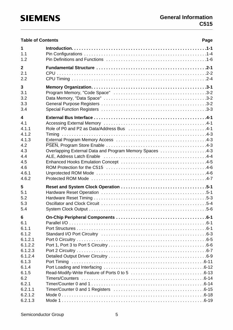
1.1 Pin Configurations
This section describes the pin configuration of the C515.
Figure 1-3 Pin Configuration of P-LCC-68 Package (top view)
P5.7P0.7
P0.5P0.6
P0.1
P2.6
P2.4
ALEPSEN
EAP0.0
P4.4
P4.5
PE/S
WD
P4.3
P5.2
P5.3
P5.5
P5.4
P5.0
P5.1
P4.0
1 689
10
2627 43
44
60
61
C515-LN/1RN
MCP00092
VCC
VAGND
P2.5
P2.7
P0.4
P2.3
P4.6
P4.7
P5.6
CCV
RESET
P6.7P6.6P6.5P6.4P6.3P6.2P6.1P6.0
RxD/P3.0TxD/P3.1
INT0/P3.2INT1/P3.3
T0/P3.4
WR/
P3.6
AREFV
P4.2
P4.1
P0.2P0.3
RD/P
3.7
T2/P
1.7
CLKO
UT/P
1.6
T2EX
/P1.
5IN
T2/P
1.4
CC3/
INT6
/P1.
3CC
2/IN
T5/P
1.2
CC1/
INT4
/P1.
1CC
0/IN
T3/P
1.0
XTAL
2XT
AL1
P2.0
P2.1
P2.2SSV
T0/P3.4T1/P3.5
Semiconductor Group 1-4

IntroductionC515
Figure 1-4 Pin Configuration of P-MQFP-80-1 Package (top view)
N.C. pins must not be connected
MCP03200
1 2
N.C.
3 4 5
P6.7
/AIN
7
6
P6.6
/AIN
6
7
P6.5
/AIN
5
8
P6.4
/AIN
4
9
P6.3
/AIN
3
10
P6.2
/AIN
2
11
P6.1
/AIN
1
12
P6.0
/AIN
0
13 14 15
P3.0
/RXD
16
P3.1
/TXD
17
P3.2
/INT0
18
P3.3
/INT1
19
P3.4
/T0
20
P3.5
/T1
V AGND
4142434445464748495051525354555657585960
P0.7
/AD7
P0.6
/AD6
P0.5
/AD5
P0.4
/AD4
P0.3
/AD3
P0.2
/AD2
P0.1
/AD1
P0.0
/AD0
EA ALE
PSEN
P2.7
/A15
P2.6
/A14
P2.5
/A13
P2.4
/A12
P2.3
/A11
P4.7P4.6P4.5P4.4P4.3
PE/SWDP4.2P4.1P4.0N.C.
P5.0P5.1P5.2P5.3P5.4P5.5
P3.6/WRP3.7/RD
P1.7/T2P1.6/CLKOUTP1.5/T2EXP1.4/INT2P1.3/INT6/CC3P1.2/INT5/CC2P1.1/INT4/CC1P1.0/INT3/CC0
XTAL2XTAL1P2.0/A8P2.1/A962
636465666768697071727374757677787980
39383736353433323130292827262524232221
4061P5.6
P5.7
SSV
CCV
P2.2/A10
AREF
VRESE
T
C515
N.C.
VCCN.
C.N.
C.N.C.
N.C.
N.C.
N.C.
N.C.
N.C.
N.C.
Semiconductor Group 1-5

IntroductionC515
1.2 Pin Definitions and Functions
This section describes all external signals of the C515 with its function.
Table 1-1 Pin Definitions and Functions
Symbol Pin NumberP-LCC-
68
Pin NumberP-MQFP-
80
I/O*) Function
P4.0-P4.7 1-3, 5-9 72-74,76-80
I/O Port 4is an 8-bit quasi-bidirectional I/O port with internal pull-up resistors. Port 4 pins that have 1’s written to them are pulled high by the internal pull-up resistors, and in that state can be used as inputs. As inputs, port 4 pins being externally pulled low will source current (I IL, in the DC characteristics) because of the internal pull-up resistors.
PE/SWD 4 75 I Power saving mode enable /Start watchdog timerA low level at this pin allows the software to enter the power saving modes(idle mode, slow down mode and power down mode). It is impossible to enter the software controlled power saving modes if this pin is held at high level. A high level during the reset performs an automatic start of watchdog timer immidiately after reset.When left unconnected this pin is pulled high by a weak internal pull-up resistor.
RESET 10 1 I RESETA low level on this pin for the duration of two machine cycles while the oscillator is running resets the C515. A small internal pullup resistor permits power-on reset using only a capacitor connected to VSS .
VAREF 11 3 – Reference voltage for the A/D converter
VAGND 12 4 – Reference ground for the A/D converter
P6.0-P6.7 13-20 5-12 I Port 6is an 8-bit unidirectional input port to the A/D converter. Port pins can be used for digital input, if voltage levels simultaneously meet the specifications for high/low input voltages and for the eight multiplexed analog inputs.
*) I = InputO = Output
Semiconductor Group 1-6

IntroductionC515
P3.0-P3.7 21-28
21
22
23
24
252627
28
15-22
15
16
17
18
192021
22
I/O Port 3is an 8-bit quasi-bidirectional I/O port with internal pullup resistors. Port 3 pins that have 1's written to them are pulled high by the internal pullup resistors, and in that state can be used as inputs. As inputs, port 3 pins being externally pulled low will source current (I IL, in the DC characteristics) because of the internal pullup resistors. Port 3 also contains the interrupt, timer, serial port and external memory strobe pins that are used by various options. The output latch corresponding to a secondary function must be programmed to a one (1) for that function to operate. The secondary functions are assigned to the pins of port 3 as follows: P3.0 / RxD Receiver data input (asynch.) or data
input/output (synch.) of serial interfaceP3.1 / TxD Transmitter data output (asynch.) or
clock output (synch.) of serial interfaceP3.2 / INT0 External interrupt 0 input /
timer 0 gate control inputP3.3 / INT1 External interrupt 1 input /
timer 1 gate control inputP3.4 / T0 Timer 0 counter inputP3.5 / T1 Timer 1 counter inputP3.6 / WR WR control output; latches the data byte
from port 0 into the external data memory
P3.7 / RD RD control output; enables theexternal data memory
*) I = InputO = Output
Table 1-1 Pin Definitions and Functions (cont’d)
Symbol Pin NumberP-LCC-
68
Pin NumberP-MQFP-
80
I/O*) Function
Semiconductor Group 1-7

IntroductionC515
P1.0 - P1.7 36-29
36
35
34
33
3231
3029
31-24
31
30
29
28
2726
2524
I/O Port 1is an 8-bit quasi-bidirectional I/O port with internal pullup resistors. Port 1 pins that have 1's written to them are pulled high by the internal pullup resistors, and in that state can be used as inputs. As inputs, port 1 pins being externally pulled low will source current (I IL, in the DC characteristics) because of the internal pullup resistors. The port is used for the low-order address byte during program verification. Port 1 also contains the interrupt, timer, clock, capture and compare pins that are used by various options. The output latch corresponding to a secondary function must be programmed to a one (1) for that function to operate (except when used for the compare functions). The secondary functions are assigned to the port 1 pins as follows :P1.0 / INT3 / CC0 Interrupt 3 input /
compare 0 output /capture 0 input
P1.1 / INT4 / CC1 Interrupt 4 input /compare 1 output /capture 1 input
P1.2 / INT5 / CC2 Interrupt 5 input /compare 2 output / capture 2 input
P1.3 / INT6 / CC3 Interrupt 6 input /compare 3 output /capture 3 input
P1.4 / INT2 Interrupt 2 inputP1.5 / T2EX Timer 2 external reload /
trigger inputP1.6 / CLKOUT System clock outputP1.7 / T2 Counter 2 input
VSS 38 34 – Ground (0 V)
VCC 37, 68 33, 69 – Supply voltageduring normal, idle, and power-down operation.
*) I = InputO = Output
Table 1-1 Pin Definitions and Functions (cont’d)
Symbol Pin NumberP-LCC-
68
Pin NumberP-MQFP-
80
I/O*) Function
Semiconductor Group 1-8

IntroductionC515
XTAL2 39 36 – XTAL2Input to the inverting oscillator amplifier and input to the internal clock generator circuits.To drive the device from an external clock source, XTAL2 should be driven, while XTAL1 is left unconnected. Minimum and maximum high and low times as well as rise/fall times specified in the AC characteristics must be observed.
XTAL1 40 37 – XTAL1Output of the inverting oscillator amplifier.
P2.0-P2.7 41-48 38-45 I/O Port 2is an 8-bit quasi-bidirectional I/O port with internal pullup resistors. Port 2 pins that have 1's written to them are pulled high by the internal pullup resistors, and in that state can be used as inputs. As inputs, port 2 pins being externally pulled low will source current (I IL, in the DC characteristics) because of the internal pullup resistors.Port 2 emits the high-order address byte during fetches from external program memory and during accesses to external data memory that use 16-bit addresses (MOVX @DPTR). In this application it uses strong internal pullup resistors when issuing 1's. During accesses to external data memory that use 8-bit addresses (MOVX @Ri), port 2 issues the contents of the P2 special function register.
PSEN 49 47 O The Program Store Enableoutput is a control signal that enables the external program memory to the bus during external fetch operations. It is activated every six oscillator periods, except during external data memory accesses. The signal remains high during internal program execution.
*) I = InputO = Output
Table 1-1 Pin Definitions and Functions (cont’d)
Symbol Pin NumberP-LCC-
68
Pin NumberP-MQFP-
80
I/O*) Function
Semiconductor Group 1-9

IntroductionC515
ALE 50 48 O The Address Latch enableoutput is used for latching the address into external memory during normal operation. It is activated every six oscillator periods, except during an external data memory access.
EA 51 49 I External Access EnableWhen held high, the C515 executes instructions from the internal ROM (C515-1R) as long as the program counter is less than 2000H. When held low, the C515 fetches all instructions from ext. program memory. For the C515-L this pin must be tied low.
P0.0-P0.7 52-59 52-59 I/O Port 0is an 8-bit open-drain bidirectional I/O port. Port 0 pins that have 1's written to them float, and in that state can be used as high-impedance inputs. Port 0 is also the multiplexed low-order address and data bus during accesses to external program and data memory. In this application it uses strong internal pullup resistors when issuing 1's. Port 0 also outputs the code bytes during program verification in the C515-1R. External pullup resistors are required during program verification.
P5.ß-P5.7 67-60 67-60 I/O Port 5 is an 8-bit quasi-bidirectional I/O port with internal pullup resistors. Port 5 pins that have 1's written to them are pulled high by the internal pullup resistors, and in that state can be used as inputs. As inputs, port 5 pins being externally pulled low will source current (I IL, in the DC characteristics) because of the internal pullup resistors.
N.C. – 2, 13, 14, 23, 32, 35, 46, 50, 51, 68, 70, 71
– Not connectedThese pins of the P-MQFP-80 package must not be connected.
*) I = InputO = Output
Table 1-1 Pin Definitions and Functions (cont’d)
Symbol Pin NumberP-LCC-
68
Pin NumberP-MQFP-
80
I/O*) Function
Semiconductor Group 1-10

Fundamental StructureC515
2 Fundamental Structure
The C515 is fully compatible to the architecture of the standard 8051/C501 microcontroller family.While maintaining all architectural and operational characteristics of the C501, the C515incorporates a 8-bit A/D converter, a timer 2 with capture/compare functions, as well as someenhancements in the Fail Save Mechanism unit. Figure 2-1 shows a block diagram of the C515.
Figure 2-1 Block Diagram of the C515
MCB03201
OSC & Timing
CPU
Timer 0
Timer 1
Timer 2
S & H
256 x 8RAM ROM
Port 0
Port 1
Port 2
Port 3
Port 0
Port 1
Port 2
XTAL2XTAL1
RESET
ALE
EA
SupportEmulation
LogicProgrammable
Watchdog Timer
PSEN
PE/SWD
Port 6
Port 5
Port 4
8 Bit Digital I/O
8 Bit Digital I/O
8K x 8
Baud Rate Generator
Digital Input
Port 5
Port 4
Port 3
Port 6
Interrupt Unit
USART
C515
8-BitA/D Converter
Reference VoltagesProgrammableVAREF
AGNDV
8 Bit Digital I/O
8 Bit Digital I/O
8 Bit Digital I/O
8 Bit Digital I/O
8 Bit Digital I/O
AnalogMUX
Semiconductor Group 2-1

Fundamental StructureC515
2.1 CPU
The C515 is efficient both as a controller and as an arithmetic processor. It has extensive facilitiesfor binary and BCD arithmetic and excels in its bit-handling capabilities. Efficient use of programmemory results from an instruction set consisting of 44% one-byte, 41% two-byte, and 15% three-byte instructions. With a 12 MHz external clock, 58% of the instructions execute in 1.0 ms (24 MHz500 ns).
The CPU (Central Processing Unit) of the C515 consists of the instruction decoder, the arithmeticsection and the program control section. Each program instruction is decoded by the instructiondecoder. This unit generates the internal signals controlling the functions of the individual unitswithin the CPU. They have an effect on the source and destination of data transfers and control theALU processing.
The arithmetic section of the processor performs extensive data manipulation and is comprised ofthe arithmetic/logic unit (ALU), an A register, B register and PSW register.
The ALU accepts 8-bit data words from one or two sources and generates an 8-bit result under thecontrol of the instruction decoder. The ALU performs the arithmetic operations add, substract,multiply, divide, increment, decrement, BDC-decimal-add-adjust and compare, and the logicoperations AND, OR, Exclusive OR, complement and rotate (right, left or swap nibble (left four)).Also included is a Boolean processor performing the bit operations as set, clear, complement, jump-if-not-set, jump-if-set-and-clear and move to/from carry. Between any addressable bit (or itscomplement) and the carry flag, it can perform the bit operations of logical AND or logical OR withthe result returned to the carry flag.
The program control section controls the sequence in which the instructions stored in programmemory are executed. The 16-bit program counter (PC) holds the address of the next instruction tobe executed. The conditional branch logic enables internal and external events to the processor tocause a change in the program execution sequence.
Accumulator
ACC is the symbol for the accumulator register. The mnemonics for accumulator-specificinstructions, however, refer to the accumulator simply as A.
Program Status Word
The Program Status Word (PSW) contains several status bits that reflect the current state of theCPU.
Semiconductor Group 2-2

Fundamental StructureC515
Special Function Register PSW (Address D0 H) Reset Value : 00 H
B Register
The B register is used during multiply and divide and serves as both source and destination. Forother instructions it can be treated as another scratch pad register.
Stack Pointer
The stack pointer (SP) register is 8 bits wide. It is incremented before data is stored during PUSHand CALL executions and decremented after data is popped during a POP and RET (RETI)execution, i.e. it always points to the last valid stack byte. While the stack may reside anywhere inthe on-chip RAM, the stack pointer is initialized to 07H after a reset. This causes the stack to begina location = 08H above register bank zero. The SP can be read or written under software control.
Bit Function
CY Carry FlagUsed by arithmetic instruction.
AC Auxiliary Carry FlagUsed by instructions which execute BCD operations.
F0 General Purpose Flag
RS1RS0
Register Bank select control bitsThese bits are used to select one of the four register banks.
OV Overflow FlagUsed by arithmetic instruction.
F1 General Purpose Flag
P Parity FlagSet/cleared by hardware after each instruction to indicate an odd/evennumber of "one" bits in the accumulator, i.e. even parity.
CY AC F0 RS1 RS0 OV F1 PD0H PSW
D7H D6H D5H D4H D3H D2H D1H D0H
Bit No. MSB LSB
RS1 RS0 Function
0 0 Bank 0 selected, data address 00H-07H0 1 Bank 1 selected, data address 08H-0FH1 0 Bank 2 selected, data address 10H-17H1 1 Bank 3 selected, data address 18H-1FH
Semiconductor Group 2-3

Fundamental StructureC515
2.2 CPU Timing
A machine cycle of the C515 consists of 6 states (12 oscillator periods). Each state is devided intoa phase 1 half and a phase 2 half. Thus, a machine cycle consists of 12 oscillator periods,numbererd S1P1 (state 1, phase 1) through S6P2 (state 6, phase 2). Each state lasts for twooscillator periods. Typically, arithmetic and logic operations take place during phase 1 and internalregister-to-register transfers take place during phase 2.
The diagrams in figure 2-2 show the fetch/execute timing related to the internal states and phases.Since these internal clock signals are not user-accessible, the XTAL1 oscillator signals and the ALE(address latch enable) signal are shown for external reference. ALE is normally activated twiceduring each machine cycle: once during S1P2 and S2P1, and again during S4P2 and S5P1.
Executing of a one-cycle instruction begins at S1P2, when the op-code is latched into the instructionregister. If it is a two-byte instruction, the second reading takes place during S4 of the samemachine cycle. If it is a one-byte instruction, there is still a fetch at S4, but the byte read (which wouldbe the next op-code) is ignored (discarded fetch), and the program counter is not incremented. Inany case, execution is completed at the end of S6P2. Figures 2-2 (a) and (b) show the timing of a1-byte, 1-cycle instruction and for a 2-byte, 1-cycle instruction.
Most C515 instructions are executed in one cycle. MUL (multiply) and DIV (divide) are the onlyinstructions that take more than two cycles to complete; they take four cycles. Normally two codebytes are fetched from the program memory during every machine cycle. The only exception to thisis when a MOVX instruction is executed. MOVX is a one-byte, 2-cycle instruction that accessesexternal data memory. During a MOVX, the two fetches in the second cycle are skipped while theexternal data memory is being addressed and strobed. Figure 2-2 (c) and (d) show the timing fora normal 1-byte, 2-cycle instruction and for a MOVX instruction.
Semiconductor Group 2-4

Fundamental StructureC515
Figure 2-2 Fetch Execute Sequence
ALE
MCD03218
S1 S2 S3 S4 S5 S6 S1 S2 S3 S4 S5 S6P1 P2 P2P1 P2P1 P2P1 P2P1 P2P1 P2P1 P2P1 P2P1 P2P1 P2P1 P2P1
OSC(XTAL1)
S1 S2 S3 S4 S5 S6
ReadOpcode Opcode (Discard)
Read next
a) 1-Byte,
b) 2-Byte,
S6S5S4S3S2S1
S1 S2 S3 S4 S5 S6
d) MOVX (1-Byte, 2-Cycle)
c) 1-Byte,
Read next Opcode (Discard)
S6S5S4S3S2S1 S1 S2 S3 S4 S5 S6
Read 2ndByteOpcode
Read
ReadOpcode
Read next Opcode again
S6S5S4S3S2S1
OpcodeRead
(MOVX)
ADDR DATA
Access External Memory
(Discard)
Read nextOpcode No Fetch No Fetch
No ALE
2-Cycle Instruction,
1-Cycle Instruction,
e.g. INC DPTR
e.g. ADD A,
e.g. INC A
# Data
1-Cycle Instruction,
Read nextOpcode
Opcode againRead next
Read next Opcode again
Semiconductor Group 2-5

Memory OrganizationC515
3 Memory Organization
The C515 CPU manipulates operands in the following four address spaces:
– up to 64 Kbyte of program memory (8K on-chip program memory for C515-1R)– up to 64 Kbyte of external data memory– 256 bytes of internal data memory– a 128 byte special function register area
Figure 3-1 illustrates the memory address spaces of the C515.
Figure 3-1 C515 Memory Map
MCD03202
00 H
H7FExternal
FFFF H
"Code Space" "Data Space" "Internal Data Space"
H0000RAM
Internal
InternalRAM
FF H
H80
FunctionSpecial
Register
DirectAddress
80 H
HFFAddressIndirect
(EA = 0)1)=(EAInternal
External
HFFFF
External
H0000
2000 H
1FFFH
Semiconductor Group 3-1

Memory OrganizationC515
3.1 Program Memory, "Code Space"
The C515-1R has 8 Kbytes of read-only program memory which can be externally expanded up to64 Kbytes. If the EA pin is held high, the C515-1R executes program code out of the internal ROMunless the program counter address exceeds 1FFFH. Address locations 2000H through FFFFH arethen fetched from the external program memory. If the EA pin is held low, the C515 fetches allinstructions from the external 64K byte program memory.
3.2 Data Memory, "Data Space"
The data memory address space consists of an internal and an external memory space. Theinternal data memory is divided into three physically separate and distinct blocks : the lower 128bytes of RAM, the upper 128 bytes of RAM, and the 128 byte special function register (SFR) area.While the upper 128 bytes of data memory and the SFR area share the same address locations,they are accessed through different addressing modes. The lower 128 bytes of data memory can beaccessed through direct or register indirect addressing; the upper 128 bytes of RAM can beaccessed through register indirect addressing; the special function registers are accessible throughdirect addressing. Four 8-register banks, each bank consisting of eight 8-bit general-purposeregisters, occupy locations 0 through 1FH in the lower RAM area. The next 16 bytes, locations 20Hthrough 2FH, contain 128 directly addressable bit locations. The stack can be located anywhere inthe internal RAM area, and the stack depth can be expanded up to 256 bytes.
The external data memory can be expanded up to 64 Kbyte and can be accessed by instructionsthat use a 16-bit or an 8-bit address.
3.3 General Purpose Registers
The lower 32 locations of the internal RAM are assigned to four banks with eight general purposeregisters (GPRs) each. Only one of these banks may be enabled at a time. Two bits in the programstatus word, RS0 (PSW.3) and RS1 (PSW.4), select the active register bank (see description of thePSW in chapter 2). This allows fast context switching, which is useful when entering subroutines orinterrupt service routines.
The 8 general purpose registers of the selected register bank may be accessed by registeraddressing. With register addressing the instruction op code indicates which register is to be used.For indirect addressing R0 and R1 are used as pointer or index register to address internal orexternal memory (e.g. MOV @R0).
Reset initializes the stack pointer to location 07H and increments it once to start from location 08Hwhich is also the first register (R0) of register bank 1. Thus, if one is going to use more than oneregister bank, the SP should be initialized to a different location of the RAM which is not used fordata storage.
Semiconductor Group 3-2

Memory OrganizationC515
3.5 Special Function Registers
The registers, except the program counter and the four general purpose register banks, reside inthe special function register area.
The 43 special function registers (SFRs) include pointers and registers that provide an interfacebetween the CPU and the other on-chip peripherals. All SFRs with addresses where address bits0-2 are 0 (e.g. 80H, 88H, 90H, 98H, ..., F8H, FFH) are bitaddressable.
The SFRs of the C515 are listed in table 3-1 and table 3-2 . In table 3-1 they are organized in groupswhich refer to the functional blocks of the C515. Table 3-2 illustrates the contents of the SFRs innumeric order of their addresses.
Semiconductor Group 3-3

Memory OrganizationC515
Table 3-1 Special Function Registers - Functional Blocks
Block Symbol Name Address Contents afterReset
CPU ACCBDPHDPLPSWSPSYSCONSYSCON4)
AccumulatorB-RegisterData Pointer, High ByteData Pointer, Low ByteProgram Status Word RegisterStack PointerSystem Control RegisterSystem Control Register
E0H 1)
F0H 1)
83H82HD0H
1)
81HB1HB1H
00H00H00H00H00H07HXX1X XXXXB
3)
XXXX XXXXB3)
A/D-Converter
ADCON 2)
ADDATDAPR
A/D Converter Control RegisterA/D Converter Data RegisterA/D Converter Program Register
D8H 1)
D9HDAH
00X0 0000B 3)
00H00H
InterruptSystem
IEN0 2)
IEN1 2)
P0 2)
IP1IRCONTCON 2)
T2CON 2)
SCON 2)
Interrupt Enable Register 0Interrupt Enable Register 1Interrupt Priority Register 0Interrupt Priority Register 1Interrupt Request Control RegisterTimer Control RegisterTimer 2 Control RegisterSerial Channel Control Register
A8H1)
B8H 1)
A9HB9HC0H
1)
88H 1)
C8H 1)
98H 1)
00H00H00HX000 0000B
3)
XX00 0000B 3)
00H00H00H
Timer 0/Timer 1
TCON 2)
TH0TH1TL0TL1TMOD
Timer 0/1 Control RegisterTimer 0, High ByteTimer 1, High ByteTimer 0, Low ByteTimer 1, Low ByteTimer Mode Register
88H 1)
8CH8DH8AH8BH89H
00H00H00H00H00H00H
Compare/ CaptureUnit /Timer 2
CCENCCH1CCH2CCH3CCL1CCL2CCL3CRCHCRCLTH2
Comp./Capture Enable Reg.Comp./Capture Reg. 1, High ByteComp./Capture Reg. 2, High ByteComp./Capture Reg. 3, High ByteComp./Capture Reg. 1, Low ByteComp./Capture Reg. 2, Low ByteComp./Capture Reg. 3, Low ByteCom./Rel./Capt. Reg. High ByteCom./Rel./Capt. Reg. Low ByteTimer 2, High Byte
C1HC3HC5HC7HC2HC4HC6HCBHCAHCDH
00H00H00H00H00H00H00H00H00H00H
1) Bit-addressable special function registers2) This special function register is listed repeatedly since some bits of it also belong to other functional blocks.3) “X“ means that the value is undefined and the location is reserved 4) For C515-LN/1RN only
Semiconductor Group 3-4

Memory OrganizationC515
Ports
TL2T2CON 2)
P0P1P2P3P4P5P6
Timer 2, Low ByteTimer 2 Control RegisterPort 0Port 1Port 2Port 3Port 4Port 5Port 6, Analog/Digital Input
CCHC8H
1)
80H 1)
90H 1)
A0H 1)
B0H 1
E8H 1)
F8H 1)
DBH
00H00HFFHFFHFFHFFHFFHFFH–
SerialChannel
ADCON 2)
PCON 2)
SBUFSCON 2)
A/D Converter Control RegisterPower Control RegisterSerial Channel Buffer RegisterSerial Channel Control Register
D8H 1
87H99H98H
1)
00X0 0000B 3)
00H
XXH 3)
00HWatchdog IEN0 2)
IEN1 2)
IP0 2)
Interrupt Enable Register 0Interrupt Enable Register 1Interrupt Priority Register 0
A8H1)
B8H 1)
A9H
00H00HX000 0000B
3)
Power Saving Modes
PCON 2) Power Control Register 87H 00H
1) Bit-addressable special function registers2) This special function register is listed repeatedly since some bits of it also belong to other functional blocks.3) “X“ means that the value is undefined and the location is reserved
Table 3-1 Special Function Registers - Functional Blocks (cont’d)
Block Symbol Name Address Contents afterReset
Semiconductor Group 3-5

Memory OrganizationC515
Table 3-2 Contents of the SFRs, SFRs in Numeric Order of their Addresses
Addr Register Contentafter Reset1)
Bit 7 Bit 6 Bit 5 Bit 4 Bit 3 Bit 2 Bit 1 Bit 0
80H 2) P0 FFH .7 .6 .5 .4 .3 .2 .1 .0
81H SP 07H .7 .6 .5 .4 .3 .2 .1 .0
82H DPL 00H .7 .6 .5 .4 .3 .2 .1 .0
83H DPH 00H .7 .6 .5 .4 .3 .2 .1 .0
87H PCON 00H SMOD PDS IDLS SD GF1 GF0 PDE IDLE
87H PCON3) 00H SMOD PDS IDLS _ GF1 GF0 PDE IDLE
88H 2) TCON 00H TF1 TR1 TF0 TR0 IE1 IT1 IE0 IT0
89H TMOD 00H GATE C/T M1 M0 GATE C/T M1 M0
8AH TL0 00H .7 .6 .5 .4 .3 .2 .1 .0
8BH TL1 00H .7 .6 .5 .4 .3 .2 .1 .0
8CH TH0 00H .7 .6 .5 .4 .3 .2 .1 .0
8DH TH1 00H .7 .6 .5 .4 .3 .2 .1 .0
90H 2) P1 FFH T2 CLK-
OUTT2EX INT2 INT6 INT5 INT4 INT3
98H 2) SCON 00H SM0 SM1 SM2 REN TB8 RB8 TI RI
99H SBUF XXH .7 .6 .5 .4 .3 .2 .1 .0
A0H2) P2 FFH .7 .6 .5 .4 .3 .2 .1 .0
A8H2) IEN0 00H EAL WDT ET2 ES ET1 EX1 ET0 EX0
A9H IP0 X000-0000B
– WDTS .5 .4 .3 .2 .1 .0
B0H2) P3 FFH RD WR T1 T0 INT1 INT0 TxD RxD
B1H SYSCON X1XX XXXXB
_ _ EALE _ _ _ _ _
B1H SYSCON XXXX XXXXB
4)
_ _ _ _ _ _ _ _
B8H2) IEN1 00H EXEN2 SWDT EX6 EX5 EX4 EX3 EX2 EADC
B9H IP1 XX00-0000B
– – .5 .4 .3 .2 .1 .0
1) X means that the value is undefined and the location is reserved2) Bit-addressable special function registers3) For C515-LN/1RN only4) This register is available without function in C515-LN/1RN
Semiconductor Group 3-6

Memory OrganizationC515
C0H2) IRCON 00H EXF2 TF2 IEX6 IEX5 IEX4 IEX3 IEX2 IADC
C1H CCEN 00H COCAH3
COCAL3
COCAH2
COCAL2
COCAH1
COCAL1
COCAH0
COCAL0
C2H CCL1 00H .7 .6 .5 .4 .3 .2 .1 .0
C3H CCH1 00H .7 .6 .5 .4 .3 .2 .1 .0
C4H CCL2 00H .7 .6 .5 .4 .3 .2 .1 .0
C5H CCH2 00H .7 .6 .5 .4 .3 .2 .1 .0
C6H CCL3 00H .7 .6 .5 .4 .3 .2 .1 .0
C7H CCH3 00H .7 .6 .5 .4 .3 .2 .1 .0
C8H2) T2CON 00H T2PS I3FR I2FR T2R1 T2R0 T2CM T2I1 T2I0
CAH CRCL 00H .7 .6 .5 .4 .3 .2 .1 .0
CBH CRCH 00H .7 .6 .5 .4 .3 .2 .1 .0
CCH TL2 00H .7 .6 .5 .4 .3 .2 .1 .0
CDH TH2 00H .7 .6 .5 .4 .3 .2 .1 .0
D0H2) PSW 00H CY AC F0 RS1 RS0 OV F1 P
D8H2) ADCON 00X0-
0000B
BD CLK – BSY ADM MX2 MX1 MX0
D9H ADDAT 00H .7 .6 .5 .4 .3 .2 .1 .0
DAH DAPR 00H .7 .6 .5 .4 .3 .2 .1 .0
DBH P6 – .7 .6 .5 .4 .3 .2 .1 .0
E0H2) ACC 00H .7 .6 .5 .4 .3 .2 .1 .0
E8H2) P4 FFH .7 .6 .5 .4 .3 .2 .1 .0
F0H2) B 00H .7 .6 .5 .4 .3 .2 .1 .0
F8H2) P5 FFH .7 .6 .5 .4 .3 .2 .1 .0
1) X means that the value is undefined and the location is reserved2) Bit-addressable special function registers
Table 3-2 Contents of the SFRs, SFRs in Numeric Order of their Addresses (cont’d)
Addr Register Contentafter Reset1)
Bit 7 Bit 6 Bit 5 Bit 4 Bit 3 Bit 2 Bit 1 Bit 0
Semiconductor Group 3-7

External Bus InterfaceC515
4 External Bus Interface
The C515 allows for external memory expansion. The functionality and implementation of theexternal bus interface is identical to the common interface for the 8051 architecture with oneexception : if the C515 is used in systems with no external memory the generation of the ALE signalcan be suppressed. Resetting bit EALE in SFR SYSCON register, the ALE signal will be gated off.This feature reduces RFI emissions of the system.
4.1 Accessing External Memory
It is possible to distinguish between accesses to external program memory and external datamemory or other peripheral components respectively. This distinction is made by hardware:accesses to external program memory use the signal PSEN (program store enable) as a readstrobe. Accesses to external data memory use RD and WR to strobe the memory (alternatefunctions of P3.7 and P3.6). Port 0 and port 2 (with exceptions) are used to provide data andaddress signals. In this section only the port 0 and port 2 functions relevant to external memoryaccesses are described.
Fetches from external program memory always use a 16-bit address. Accesses to external datamemory can use either a 16-bit address (MOVX @DPTR) or an 8-bit address (MOVX @Ri).
4.1.1 Role of P0 and P2 as Data/Address Bus
When used for accessing external memory, port 0 provides the data byte time-multiplexed with thelow byte of the address. In this state, port 0 is disconnected from its own port latch, and the address/data signal drives both FETs in the port 0 output buffers. Thus, in this application, the port 0 pins arenot open-drain outputs and do not require external pullup resistors.
During any access to external memory, the CPU writes FFH to the port 0 latch (the special functionregister), thus obliterating whatever information the port 0 SFR may have been holding.
Whenever a 16-bit address is used, the high byte of the address comes out on port 2, where it isheld for the duration of the read or write cycle. During this time, the port 2 lines are disconnectedfrom the port 2 latch (the special function register).
Thus the port 2 latch does not have to contain 1s, and the contents of the port 2 SFR are notmodified.
If an 8-bit address is used (MOVX @Ri), the contents of the port 2 SFR remain at the port 2 pinsthroughout the external memory cycle. This will facilitate paging. It should be noted that, if a port 2pin outputs an address bit that is a 1, strong pullups will be used for the entire read/write cycle andnot only for two oscillator periods.
Semiconductor Group 4-1

External Bus InterfaceC515
Figure 4-1 External Program Memory Execution
PCLOUT
PCHOUT
One Machine Cycle One Machine Cycle
ININST.
IN OUTPCL PCL
OUTIN IN OUTPCL
IN
(A)withoutMOVX
PCL OUTvalid
PCL OUTvalid
PCL OUTvalid
PCL OUTvalid
ALE
PSEN
RD
P2
a)
b)
P2
RD
PSEN
ALE
validPCL OUT
validDPL or Ri
validPCL OUT
MOVXwith(B)
INPCLOUTIN
DATAININ
DPH OUT ORP2 OUT
One Machine CycleOne Machine Cycle
OUTPCL
S6S5S4S3S2S1S6S5S4S3S2S1
MCT03220
S1 S2 S3 S4 S5 S6 S1 S2 S3 S4 S5 S6
OUTPCH PCH
OUTOUTPCH
PCHOUT OUT
PCH
INST. INST. INST. INST.P0
P0 INST. INST. INST.
Semiconductor Group 4-2

External Bus InterfaceC515
4.1.2 Timing
The timing of the external bus interface, in particular the relationship between the control signalsALE, PSEN, RD, WR and information on port 0 and port 2, is illustated in figure 4-1 a) and b).
Data memory: in a write cycle, the data byte to be written appears on port 0 just before WR isactivated and remains there until after WR is deactivated. In a read cycle, theincoming byte is accepted at port 0 before the read strobe is deactivated.
Program memory: Signal PSEN functions as a read strobe.
4.1.3 External Program Memory Access
The external program memory is accessed under two conditions:- whenever signal EA is active (low); or- whenever the program counter (PC) content is greater than 1FFFH
When the CPU is executing out of external program memory, all 8 bits of port 2 are dedicated to anoutput function and must not be used for general-purpose I/O. The content of the port 2 SFRhowever is not affected. During external program memory fetches port 2 lines output the high byteof the PC, and during accesses to external data memory they output either DPH or the port 2 SFR(depending on whether the external data memory access is a MOVX @DPTR or a MOVX @Ri).
Since the C515-L has no internal program memory, accesses to program memory are alwaysexternal, and port 2 is at all times dedicated to output the high-order address byte. This means thatport 0 and port 2 of the C515-L can never be used as general-purpose I/O. This also applies to theC515-1R when it operates with only an external program memory.
4.2 PSEN, Program Store Enable
The read strobe for external program memory fetches is PSEN. It is not activated for internalprogram memory fetches. When the CPU is accessing external program memory, PSEN isactivated twice every instruction cycle (except during a MOVX instruction) no matter whether or notthe byte fetched is actually needed for the current instruction. When PSEN is activated its timing isnot the same as for RD. A complete RD cycle, including activation and deactivation of ALE and RD,takes 6 oscillator periods. A complete PSEN cycle, including activation and deactivation of ALE andPSEN, takes 3 oscillator periods. The execution sequence for these two types of read cycles isshown in figure 4-1 a) and b).
4.3 Overlapping External Data and Program Memory Spaces
In some applications it is desirable to execute a program from the same physical memory that isused for storing data. In the C515 the external program and data memory spaces can be combinedby the logical-AND of PSEN and RD. A positive result from this AND operation produces a lowactive read strobe that can be used for the combined physical memory. Since the PSEN cycle isfaster than the RD cycle, the external memory needs to be fast enough to adapt to the PSEN cycle.
Semiconductor Group 4-3

External Bus InterfaceC515
4.4 ALE, Address Latch Enable
The C515 allows to switch off the ALE output signal. If the internal ROM is used (EA=1 andPC £ 1FFFH) and ALE is switched off by EALE=0, then, ALE will only go active during external datamemory accesses (MOVX instructions). If EA=0, the ALE generation is always enabled and the bitEALE has no effect.
After a hardware reset the ALE generation is enabled.
Special Function Register SYSCON (Address B1 H) Reset Value : XX1XXXXX B
Note: The ALE swicth-off feature is available in C515-LM/1RM versions only. In case of theC515-LN/1RN versions, the SYSCON register is present without function.
Bit Function
EALE Enable ALE outputEALE = 0 : ALE generation is disabled; disables ALE signal generation
during internal code memory accesses (EA=1). With EA=1,ALE is automatically generated at MOVX instructions.
EALE = 1 : ALE generation is enabledIf EA=0, the ALE generation is always enabled and the bit EALE has noeffect on the ALE generation.
– Reserved bits for future use, read by CPU returns undefined values.
7 6 5 4 3 2 1 0
EALE – –B1H SYSCON
Bit No. MSB LSB
– –– – –
Semiconductor Group 4-4

External Bus InterfaceC515
4.5 Enhanced Hooks Emulation Concept
The Enhanced Hooks Emulation Concept of the C500 microcontroller family is a new, innovativeway to control the execution of C500 MCUs and to gain extensive information on the internaloperation of the controllers. Emulation of on-chip ROM based programs is possible, too. Each C500 production chip has built-in logic for the support of the Enhanced Hooks EmulationConcept. Therefore, no costly bond-out chips are necessary for emulation. This also ensure thatemulation and production chips are identical.
The Enhanced Hooks TechnologyTM 1), which requires embedded logic in the C500 allows the C500together with an EH-IC to function similar to a bond-out chip. This simplifies the design and reducescosts of an ICE-system. ICE-systems using an EH-IC and a compatible C500 are able to emulateall operating modes of the different versions of the C500 microcontrollers. This includes emulationof ROM, ROM with code rollover and ROMless modes of operation. It is also able to operate insingle step mode and to read the SFRs after a break.
Figure 4-2 Basic C500 MCU Enhanced Hooks Concept Configuration
Port 0, port 2 and some of the control lines of the C500 based MCU are used by Enhanced HooksEmulation Concept to control the operation of the device during emulation and to transferinformations about the program execution and data transfer between the external emulationhardware (ICE-system) and the C500 MCU.
1 “Enhanced Hooks Technology“ is a trademark and patent of Metalink Corporation licensed to Siemens.
MCS02647
SYSCONPCONTCON
RESETEA
PSENALE
Port 0
Port 2
I/O PortsOptional
Port 3 Port 1
C500MCU Interface Circuit
Enhanced Hooks
RPort 0RPort 2
RTCONRPCON
RSYSCON
TEA TALE TPSEN
EH-IC
Target System Interface
ICE-System Interfaceto Emulation Hardware
Semiconductor Group 4-5

External Bus InterfaceC515
4.6 ROM Protection for the C515
The C515-1R allows to protect the contents of the internal ROM against unauthorized read out. Thetype of ROM protection (protected or unprotected) is fixed with the ROM mask. Therefore, thecustomer of a C515-1R version has to define whether ROM protection has to be selected or not.
The C515-1R devices, which operate from internal ROM, are always checked for correct ROMcontents during production test. Therefore, unprotected as well as protected ROMs must provide aprocedure to verify the ROM contents. In ROM verification mode 1, which is used to verifyunprotected ROMs, a ROM address is applied externally to the C515-1R and the ROM data byte isoutput at port 0. ROM verification mode 2, which is used to verify ROM protected devices, operatesdifferent : ROM addresses are generated internally and the expected data bytes must be appliedexternally to the device (by the manufacturer or by the customer) and are compared internally withthe data bytes from the ROM. After 16 byte verify operations the state of the P3.5 pin shows whetherthe last 16 bytes have been verified correctly.
This mechanism provides a very high security of ROM protection. Only the owner of the ROM codeand the manufacturer who know the contents of the ROM can read out and verify it with less effort.
The behaviour of the move code instruction, when the code is executed from the external ROM, isin such a way that accessing a code byte from a protected on-chip ROM address is not possible. Inthis case the state of the EA pin is always latched with the rising edge of RESET and the byteaccessed will be invalid.
4.6.1 Unprotected ROM Mode
If the ROM is unprotected, the ROM verification mode 1 as shown in figure 4-3 is used to read outthe contents of the ROM. The AC timing characteristics of the ROM verification mode is shown inthe AC specifications (chapter 10).
Figure 4-3 ROM Verification Mode 1
ROM verification mode 1 is selected if the inputs PSEN, ALE, EA, and RESET are put to thespecified logic level. Then the 14-bit address of the internal ROM byte to be read is applied to theport 1 and port 2 lines. After a delay time, port 0 outputs the content of the addressed ROM cell. InROM verification mode 1, the C515 must be provided with a system clock at the XTAL pins andpullup resistors on the port 0 lines.
MCT03221
Inputs: PSEN = SSVALE, EA = VIH
RESET = VIL2
Address
Port 0 Data
P2.0 - P2.4P1.7-P1.0
/ IH2V
1
1 Out 2 Out
2
Data
Address
Semiconductor Group 4-6

External Bus InterfaceC515
4.6.2 Protected ROM Mode
If the ROM is protected, the ROM verification mode 2 as shown in figure 4-4 is used to verify thecontents of the ROM. The detailed timing characteristics of the ROM verification mode is shown inthe AC specifications (chapter 10).
Figure 4-4 ROM Verification Mode 2
ROM verification mode 2 is selected if the inputs PSEN, EA, and ALE are put to the specified logiclevels. With RESET going inactive, the ROM verification mode 2 sequence is started. The C515outputs an ALE signal with a period of 3 CLP and expects data bytes at port 0. The data bytes at port0 are assigned to the ROM addresses in the following way :
1. Data Byte = content of internal ROM address 0000H2. Data Byte = content of internal ROM address 0001H3. Data Byte = content of internal ROM address 0002H :16. Data Byte= content of internal ROM address 000FH :
The C515-1R does not output any address information during the ROM verification mode 2. Thefirst data byte to be verified is always the byte which is assigned to the internal ROM address 0000Hand is put onto the data bus with the first rising edge of ALE. With each following ALE pulse theROM address pointer is internally incremented and the expected data byte for the next ROMaddress must be delivered externally.Between two ALE pulses the data at port 0 is latched (at 3 CLP after ALE rising edge) and comparedinternally with the ROM content of the actual address. If an verify error is detected, the error
MCT03222
Data forAddr. 1
Low : ErrorHigh : OK
~ ~~~
~~~~
~~ ~ ~~ ~
~ ~~~
Latch Latch Latch Latch
61. ALE Pulse
after Reset
~~
Inputs : ALE = SSVPSEN, EA = VIH
RESET =
RESET
ALE
Port 0
P3.5
Data forAddr. X-16-1 Addr. X-16
Data for Data forAddr. x-16+1Addr. 0
Data for
12 t CLCL
CLCLt
Semiconductor Group 4-7

External Bus InterfaceC515
condition is stored internally. After each 16th data byte the cumulated verify result (pass or fail) ofthe last 16 verify operations is output at P3.5. This means that P3.5 stays at static level (low for failand high for pass) during the 16 bytes are checked. In ROM verification mode 2, the C515 must beprovided with a system clock at the XTAL pins.
Figure 4-5 shows an application example of an external circuitry which allows to verify a protectedROM inside the C515-1R in ROM verification mode 2. With RESET going inactive, the C515-1Rstarts the ROM verify sequence. Its ALE is clocking a 13-bit address counter. This countergenerates the addresses for an external EPROM which is programmed with the contents of theinternal (protected) ROM. The verify detect logic typically displays the pass/fail information of theverify operation. P3.5 can be latched with the falling edge of ALE.
When the last byte of the internal ROM has been handled, the C515-1R starts generating a PSENsignal. This signal or the CY signal of the address counter indicate to the verify detect logic the endof the internal ROM verification.
Figure 4-5 ROM Verification Mode 2 - External Circuitry Example
MCS03223
&
&
CCV
Carry
S
2 kW A0
CS OE
D0
P3.5
ALE
RESET
0Port
C515-1R
CCVEA
PSEN
CLK
-
- A12
D7
LogicDetectVerify
AddressBit
Counter
13-
CompareCodeROM
Semiconductor Group 4-8

Reset / System ClockC515
5 Reset and System Clock Operation
5.1 Hardware Reset Operation
The hardware reset function incorporated in the C515 allows for an easy automatic start-up at aminimum of additional hardware and forces the controller to a predefined default state. Thehardware reset function can also be used during normal operation in order to restart the device. Thisis particularly done when the power-down mode is to be terminated.
Additional to the hardware reset, which is applied externally to the C515, there exists anotherinternal reset source, the watchdog timer. This chapter deals only with the external hardware reset.
The reset input is an active low input. An internal Schmitt trigger is used at the input for noiserejection. Since the reset is synchronized internally, the RESET pin must be held low for at least twomachine cycles (24 oscillator periods) while the oscillator is running. With the oscillator running theinternal reset is executed during the second machine cycle and is repeated every cycle until RESETgoes high again.
During reset, pins ALE and PSEN are configured as inputs and should not be stimulated or drivenexternally. (An external stimulation at these lines during reset activates several test modes whichare reserved for test purposes. This in turn may cause unpredictable output operations at severalport pins).
At the reset pin, a pullup resistor is internally connected to VCC to allow a power-up reset with anexternal capacitor only. An automatic power-up reset can be obtained when VCC is applied byconnecting the reset pin to VSS via a capacitor. After VCC has been turned on, the capacitor must holdthe voltage level at the reset pin for a specific time to effect a complete reset.
Semiconductor Group 5-1

Reset / System ClockC515
The time required for a reset operation is the oscillator start-up time plus 2 machine cycles, which,under normal conditions, must be at least 10 - 20 ms for a crystal oscillator. This requirement istypically met using a capacitor of 4.7 to 10 mF. The same considerations apply if the reset signal isgenerated externally (figure 5-1 b ). In each case it must be assured that the oscillator has startedup properly and that at least two machine cycles have passed before the reset signal goes inactive.
Figure 5-1 Reset Circuitries
A correct reset leaves the processor in a defined state. The program execution starts at location0000H. After reset is internally accomplished the port latches are set to FFH. This leaves port 0floating, since it is an open drain port when not used as data/address bus. All other I/O port lines(ports 1 to 5) output a one (1). Port 6 is an input-only port. It has no internal latch and therefore thecontents of the special function registers P6 depend on the levels applied to port 6.
The content of the internal RAM of the C515 is not affected by a reset. After power-up the contentis undefined, while it remains unchanged during a reset if the power supply is not turned off.
MCS03203
RESET
C515
b)a)
c)
+
+
&
RESET
RESET
C515
C515
Semiconductor Group 5-2

Reset / System ClockC515
5.2 Hardware Reset Timing
This section describes the timing of the hardware reset signal.
The input pin RESET is sampled once during each machine cycle. This happens in state 5 phase2. Thus, the external reset signal is synchronized to the internal CPU timing. When the reset isfound active (low level) the internal reset procedure is started. It needs two complete machinecycles to put the complete device to its correct reset state, i.e. all special function registers containtheir default values, the port latches contain 1's etc. Note that this reset procedure is also performedif there is no clock available at the device. (This is done by the oscillator watchdog, which providesan auxiliary clock for performing a perfect reset without clock at the XTAL1 and XTAL2 pins). TheRESET signal must be active for at least one machine cycle; after this time the C515 remains in itsreset state as long as the signal is active. When the signal goes inactive this transition is recognizedin the following state 5 phase 2 of the machine cycle. Then the processor starts its address output(when configured for external ROM) in the following state 5 phase 1. One phase later (state 5 phase2) the first falling edge at pin ALE occurs.
Figure 5-2 shows this timing for a configuration with EA = 0 (external program memory). Thus,between the release of the RESET signal and the first falling edge at ALE there is a time period ofat least one machine cycle but less than two machine cycles.
Figure 5-2 CPU Timing after Reset
MCT01879
S4 S5 S6 S1 S2 S3 S4 S5 S6 S1 S2 S3 S4 S5 S6 S1 S2
P1 P2
PCLOUT
PCLOUT
PCHOUT
PCHOUT
One Machine Cycle
RESET
P0
P2
ALE
INInst.
Semiconductor Group 5-3

Reset / System ClockC515
5.3 Oscillator and Clock Circuit
XTAL1 and XTAL2 are the output and input of a single-stage on-chip inverter which can beconfigured with off-chip components as a Pierce oscillator. The oscillator, in any case, drives theinternal clock generator. The clock generator provides the internal clock signals to the chip. Thesesignals define the internal phases, states and machine cycles.
Figure 5-3 shows the recommended oscillator circuit.
Figure 5-3 Recommended Oscillator Circuitry
In this application the on-chip oscillator is used as a crystal-controlled, positive-reactance oscillator(a more detailed schematic is given in figure 5-4 ). lt is operated in its fundamental response modeas an inductive reactor in parallel resonance with a capacitor external to the chip. The crystalspecifications and capacitances are non-critical. In this circuit 20 pF can be used as singlecapacitance at any frequency together with a good quality crystal. A ceramic resonator can be usedin place of the crystal in cost-critical applications. If a ceramic resonator is used, the two capacitorsnormally have different values depending on the oscillator frequency. We recommend consultingthe manufacturer of the ceramic resonator for value specifications of these capacitors.
MCS03225
C
C
C = 20 pF ± 10 pF for Crystal Operation
XTAL2
XTAL1
C515- 24 MHz1
Semiconductor Group 5-4

Reset / System ClockC515
Figure 5-4 On-Chip Oscillator Circuitry
To drive the C515 with an external clock source, the external clock signal has to be applied toXTAL2, as shown in figure 5-5 . XTAL1 has to be left unconnected. A pullup resistor is suggested(to increase the noise margin), but is optional if VOH of the driving gate corresponds to the VIH2
specification of XTAL2.
Figure 5-5 External Clock Source
MCS03226
C515
XTAL1 XTAL2
To InternalTiming Circuitry
1C C 2
1)
1) Crystal or Ceramic Resonator
MCS03227
XTAL1
XTAL2ExternalClock
VCC
Signal
N.C.
C515
Semiconductor Group 5-5

Reset / System ClockC515
5.4 System Clock Output
For peripheral devices requiring a system clock, the C515 provides a clock output signal derivedfrom the oscillator frequency as an alternate output function on pin P1.6/CLKOUT. lf bit CLK is set(bit 6 of special function register ADCON), a clock signal with 1/12 of the oscillator frequency isgated to pin P1.6/CLKOUT. To use this function the port pin must be programmed to a one (1),which is also the default after reset.
Special Function Register ADCON (Address D8 H) Reset Value : 00X000000 B
The system clock is high during S3P1 and S3P2 of every machine cycle and low during all otherstates. Thus, the duty cycle of the clock signal is 1:6. Associated with a MOVX instruction thesystem clock coincides with the last state (S3) in which a RD or WR signal is active. A timingdiagram of the system clock output is shown in figure 5-6 .
Note : During slow-down operation the frequency of the CLKOUT signal is divided by 8.
Bit Function
CLK Clockout enable bitWhen set, pin P1.6/CLKOUT outputs the system clock which is 1/12 of the oscillator frequency.
– Reserved bit for future use. Read by CPU returns undefined value.
BD CLK – BSYD8H ADCON
Bit No. DFH DEH DDH DCH DBH DAH D9H D8H
MSB LSB
ADM MX2 MX1 MX0
The shaded bits are not used for clock output control.
Semiconductor Group 5-6

Reset / System ClockC515
Figure 5-6 Timing Diagram - System Clock Output
MCT01858
S6 S1 S2 S3 S4 S5 S6 S1 S2 S3 S4 S5 S6 S1 S2
ALE
PSEN
RD,WR
CLKOUT
Semiconductor Group 5-7

On-Chip Peripheral ComponentsC515
6 On-Chip Peripheral Components
This chapter gives detailed information about all on-chip peripherals of the C515 except for theintegrated interrupt controller, which is described separately in chapter 7 .
6.1 Parallel I/O
The C515 has six 8-bit I/O ports and one 8-bit input port for analog/digital input. Port 0 is an open-drain bidirectional I/O port, while ports 1 to 5 are quasi-bidirectional I/O ports with internal pullupresistors. That means, when configured as inputs, ports 1 to 5 will be pulled high and will sourcecurrent when externally pulled low. Port 0 will float when configured as input.
The output drivers of port 0 and 2 and the input buffers of port 0 are also used for accessing externalmemory. In this application, port 0 outputs the low byte of the external memory address, timemultiplexed with the byte being written or read. Port 2 outputs the high byte of the external memoryaddress when the address is 16 bits wide. Otherwise, the port 2 pins continue emitting the P2 SFRcontents. In this function, port 0 is not an open-drain port, but uses a strong internal pullup FET .
6.1.1 Port Structures
The C515 generally allows digital I/O on 48 lines grouped into 6 bidirectional C501 compatible 8-bitports and one 8-bit analog/digital input port. Each port bit (except port 6) consists of a latch, anoutput driver and an input buffer. Read and write accesses to the I/O ports P0 to P5 are performedvia their corresponding special function registers. Depending on the specific ports, multiplefunctions are assigned to the port pins. These alternate functions of the port pins are listed intable 6-1 .
When port 6 is used as analog input, an analog channel is switched to the A/D converter through a3-bit multiplexer, which is controlled by three bits in SFR ADCON (see chapter 6.4 ). Port 6 linesmay also be used as digital inputs. In this case they are addressed as an input port via SFR P6.Since port 6 has no internal latch, the contents of SFR P6 only depends on the levels applied to theinput lines. It makes no sense to output a value to these input-only port by writing to the SFR P6.This will have no effect.
Semiconductor Group 6-1

On-Chip Peripheral ComponentsC515
Table 6-1 Alternate Functions of Port 1 and 3
Port Alternate Functions
Description
P1.0P1.1P1.2P1.3P1.4P1.5P1.6P1.7
P3.0
P3.1
P3.2P3.3P3.4P3.5P3.6P3.7
INT3 / CC0INT4 / CC1INT5 / CC2INT6 / CC3INT2T2EXCLKOUTT2
RxD
TxD
INT0INT1T0T1WRRD
External Interrupt 3 input / Capture/compare 0 input/outputExternal Interrupt 4 input / Capture/compare 1 input/outputExternal Interrupt 5 input / Capture/compare 2 input/outputExternal Interrupt 6 input / Capture/compare 3 input/outputExternal Interrupt 2 inputTimer 2 external reload/trigger inputSystem clock outputTimer 2 external count input
Serial port’s receiver data input (asynchronous) or data input/output (synchronous)Serial port’s transmitter data output (asynchronous) or data clock output (synchronous)External interrupt 0 input, timer 0 gate controlExternal interrupt 1 input, timer 1 gate controlTimer 0 external count inputTimer 1 external count inputExternal data memory write strobeExternal data memory read strobe
Semiconductor Group 6-2

On-Chip Peripheral ComponentsC515
6.1.2 Standard I/O Port Circuitry
Figure 6-1 shows a functional diagram of a typical bit latch and I/O buffer, which is the core of eachof the six I/O-ports. The bit latch (one bit in the port’s SFR) is represented as a type-D flip-flop, whichwill clock in a value from the internal bus in response to a "write-to-latch" signal from the CPU. TheQ output of the flip-flop is placed on the internal bus in response to a "read-latch" signal from theCPU. The level of the port pin itself is placed on the internal bus in response to a "read-pin" signalfrom the CPU. Some instructions that read from a port (i.e. from the corresponding port SFR P0 toP4) activate the "read-latch" signal, while others activate the "read-pin" signal.
Figure 6-1 Basic Structure of a Port Circuitry
MCS01822
D
CLK
PortLatch
Q
Q
Port
ReadLatch
toLatch
ReadPin
Write
Int. BusPortDriverCircuit
Pin
Semiconductor Group 6-3

On-Chip Peripheral ComponentsC515
The output drivers of port 1 to 5 have internal pullup FET’s (see figure 6-2 ). Each I/O line can beused independently as an input or output. To be used as an input, the port bit stored in the bit latchmust contain a one (1) (that means for figure 6-2 : Q=0), which turns off the output driver FET n1.Then, for ports 1 to 5 the pin is pulled high by the internal pullups, but can be pulled low by anexternal source. When externally pulled low the port pins source current (IIL or ITL). For this reasonthese ports are called "quasi-bidirectional".
Figure 6-2 Basic Output Driver Circuit of Ports 1 to 5
MCS01823
D
CLK
BitLatch
Q
Q
InternalPull UpArrangement
Pin
ReadLatch
toLatch
ReadPin
Write
VCC
Int. Bus
n1
Semiconductor Group 6-4
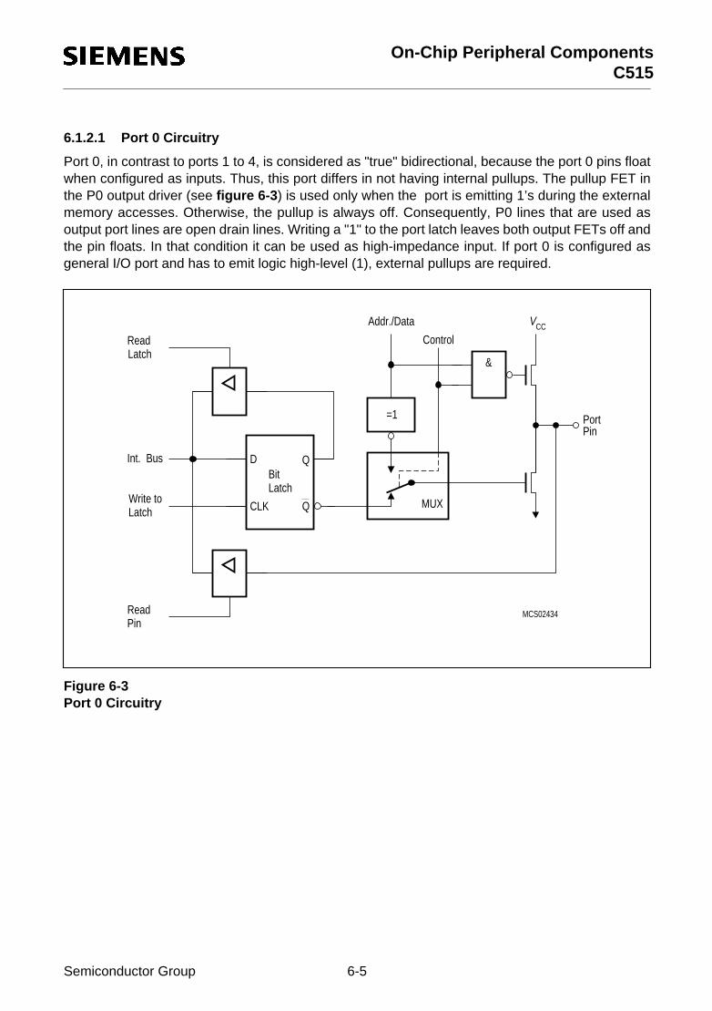
On-Chip Peripheral ComponentsC515
6.1.2.1 Port 0 Circuitry
Port 0, in contrast to ports 1 to 4, is considered as "true" bidirectional, because the port 0 pins floatwhen configured as inputs. Thus, this port differs in not having internal pullups. The pullup FET inthe P0 output driver (see figure 6-3 ) is used only when the port is emitting 1’s during the externalmemory accesses. Otherwise, the pullup is always off. Consequently, P0 lines that are used asoutput port lines are open drain lines. Writing a "1" to the port latch leaves both output FETs off andthe pin floats. In that condition it can be used as high-impedance input. If port 0 is configured asgeneral I/O port and has to emit logic high-level (1), external pullups are required.
Figure 6-3 Port 0 Circuitry
MCS02434
D
CLK
BitLatch
Control
Addr./Data
MUX
Pin
ReadLatch
Bus
Latch
ReadPin
Write to
VCC
Int.
&
Port=1
Q
Q
Semiconductor Group 6-5

On-Chip Peripheral ComponentsC515
6.1.2.2 Port 1, Port 3 to Port 5 Circuitry
The pins of ports 1, 3, 4, and 5 are multifunctional. They are port pins and also serve to implementspecial features as listed in table 6-1 .
Figure 6-4 shows a functional diagram of a port latch with alternate function. To pass the alternatefunction to the output pin and vice versa, however, the gate between the latch and driver circuit mustbe open. Thus, to use the alternate input or output functions, the corresponding bit latch in the portSFR has to contain a one (1); otherwise the pulldown FET is on and the port pin is stuck at 0. Afterreset all port latches contain ones (1).
Figure 6-4 Ports 1, 3, 4 and 5
MCS01827
D
CLK
BitLatch
Q
Q
InternalPull UpArrangement
Pin
ReadLatch
toLatch
ReadPin
Write
VCC
Int. Bus
AlternateOutput
Function
AlternateInput
Function
&
Semiconductor Group 6-6

On-Chip Peripheral ComponentsC515
6.1.2.3 Port 2 Circuitry
As shown in figure 6-3 and below in figure 6-5 , the output drivers of ports 0 and 2 can be switchedto an internal address or address/data bus for use in external memory accesses. In this applicationthey cannot be used as general purpose I/O, even if not all address lines are used externally. Theswitching is done by an internal control signal dependent on the input level at the EA pin and/or thecontents of the program counter. If the ports are configured as an address/data bus, the port latchesare disconnected from the driver circuit. During this time, the P0/P2 SFR remains unchanged. Beingan address/data bus, port 0 uses a pullup FET as shown in figure 6-3 . When a 16-bit address isused, port 2 uses the additional strong pullups p1 (figure 6-6 ) to emit 1’s for the entire externalmemory cycle instead of the weak ones (p2 and p3) used during normal port activity.
Figure 6-5 Port 2 Circuitry
If no external bus cycles are generated using data or code memory accesses, port 0 can be usedfor I/O functions.
MCS03228
D
CLK
BitLatch
ControlAddr.
MUX
Pin
ReadLatch
Latch
ReadPin
Write to
VCC
Int. Bus
Port
=1
Q
Q
InternalPull Up
Arrangement
Semiconductor Group 6-7

On-Chip Peripheral ComponentsC515
Figure 6-6 Port 2 Pull-up Arrangement
Port 2 in I/O function works similar to the standard port driver circuitry (section 6.1.2.4) whereas inaddress output function it works similar to Port 0 circuitry.
MCS03229
1
1
= 1= 1
VCC
PortPin
SSV
Input Data (Read Pin)
Delay p1 p2 p3
n1= 1
MUX
Addr. Control
Q
1 State
_<
_<
Semiconductor Group 6-8

On-Chip Peripheral ComponentsC515
6.1.2.4 Detailed Output Driver Circuitry
In fact, the pullups mentioned before and included in figure 6-2, 6-4 and 6-5 are pulluparrangements.
Figure 6-7 shows the detailed output driver (pullup arrangement) circuit of the the port 1 and 3 to 5port lines. The basic circuitry of these ports is shown in figure 6-4 . The pullup arrangement of theseport lines has one n-channel pulldown FET and three pullup FETs:
Figure 6-7 Driver Circuit of Ports 1, 3 to 6
– The pulldown FET n1 is of n-channel type. It is a very strong driver transistor which is capableof sinking high currents (IOL); it is only activated if a "0" is programmed to the port pin. A shortcircuit to VCC must be avoided if the transistor is turned on, since the high current might destroythe FET. This also means that no “0“ must be programmed into the latch of a pin that is usedas input.
– The pullup FET p1 is of p-channel type. It is activated for two oscillator periods (S1P1 andS1P2) if a 0-to-1 transition is programmed to the port pin, i.e. a "1" is programmed to the portlatch which contained a "0". The extra pullup can drive a similar current as the pulldown FETn1. This provides a fast transition of the logic levels at the pin.
– The pullup FET p2 is of p-channel type. It is always activated when a "1" is in the port latch,thus providing the logic high output level. This pullup FET sources a much lower current thanp1; therefore the pin may also be tied to ground, e.g. when used as input with logic low inputlevel.
MCS03230
=11
=1=1
VCC
PortPin
SSV
Q
Input Data(Read Pin)
p1 p2 p3
n1
Delay = 1 State
_<
Semiconductor Group 6-9

On-Chip Peripheral ComponentsC515
– The pullup FET p3 is of p-channel type. It is only activated if the voltage at the port pin ishigher than approximately 1.0 to 1.5 V. This provides an additional pullup current if a logichigh level shall be output at the pin (and the voltage is not forced lower than approximately1.0 to 1.5 V). However, this transistor is turned off if the pin is driven to a logic low level, e.gwhen used as input. In this configuration only the weak pullup FET p2 is active, which sourcesthe current IIL . If, in addition, the pullup FET p3 is activated, a higher current can be sourced(ITL). Thus, an additional power consumption can be avoided if port pins are used as inputswith a low level applied. However, the driving capability is stronger if a logic high level isoutput.
The described activating and deactivating of the four different transistors translates into four statesthe pins can be:
– input low state (IL), p2 active only– input high state (IH) = steady output high state (SOH) p2 and p3 active– forced output high state (FOH), p1, p2 and p3 active– output low state (OL), n1 active
If a pin is used as input and a low level is applied, it will be in IL state, if a high level is applied, it willswitch to IH state.
If the latch is loaded with "0", the pin will be in OL state.
If the latch holds a "0" and is loaded with "1", the pin will enter FOH state for two cycles and thenswitch to SOH state. If the latch holds a "1" and is reloaded with a "1" no state change will occur.
At the beginning of power-on reset the pins will be in IL state (latch is set to "1", voltage level on pinis below of the trip point of p3). Depending on the voltage level and load applied to the pin, it willremain in this state or will switch to IH (=SOH) state.If it is used as output, the weak pull-up p2 will pull the voltage level at the pin above p3’s trip pointafter some time and p3 will turn on and provide a strong "1". Note, however, that if the load exceedsthe drive capability of p2 (IIL), the pin might remain in the IL state and provide a week "1" until thefirst 0-to-1 transition on the latch occurs. Until this the output level might stay below the trip point ofthe external circuitry.
The same is true if a pin is used as bidirectional line and the external circuitry is switched fromoutput to input when the pin is held at "0" and the load then exceeds the p2 drive capabilities.
If the load exceeds IIL the pin can be forced to "1" by writing a "0" followed by a "1" to the port pin.
Semiconductor Group 6-10

On-Chip Peripheral ComponentsC515
6.1.3 Port Timing
When executing an instruction that changes the value of a port latch, the new value arrives at thelatch during S6P2 of the final cycle of the instruction. However, port latches are only sampled bytheir output buffers during phase 1 of any clock period (during phase 2 the output buffer holds thevalue it noticed during the previous phase 1). Consequently, the new value in the port latch will notappear at the output pin until the next phase 1, which will be at S1P1 of the next machine cycle.
When an instruction reads a value from a port pin (e.g. MOV A, P1) the port pin is actually sampledin state 5 phase 1 or phase 2 depending on port and alternate functions. Figure 6-8 illustrates thisport timing. It must be noted that this mechanism of sampling once per machine cycle is also usedif a port pin is to detect an "edge", e.g. when used as counter input. In this case an "edge" isdetected when the sampled value differs from the value that was sampled the cycle before.Therefore, there must be met certain reqirements on the pulse length of signals in order to avoidsignal "edges" not being detected. The minimum time period of high and low level is one machinecycle, which guarantees that this logic level is noticed by the port at least once.
Figure 6-8 Port Timing
MCT03231
P1 P2S4 S5
P2P1S6
P2P1S1
P2P1S2
P2P1S3
P2P1
XTAL2
Input sampled:e.g. MOV A, P1
Old Data New DataPort
P1 active for 1 State(driver transistor)
Semiconductor Group 6-11

On-Chip Peripheral ComponentsC515
6.1.4 Port Loading and Interfacing
The output buffers of ports 1 to 5 can drive TTL inputs directly. The maximum port load which stillguarantees correct logic output levels can be be looked up in the DC characteristics in the DataSheet of the C515 or in chapter 10 of this User’s Manual. The corresponding parameters are VOL
and VOH.
The same applies to port 0 output buffers. They do, however, require external pullups to drivefloating inputs, except when being used as the address/data bus.
When used as inputs it must be noted that the ports 1 to 5 are not floating but have internal pulluptransistors. The driving devices must be capable of sinking a sufficient current if a logic low levelshall be applied to the port pin (the parameters ITL and IIL in the DC characteristics specify thesecurrents). Port 0 as well as port 1 programmed to analog input function, however, have floatinginputs when used for digital input.
Semiconductor Group 6-12

On-Chip Peripheral ComponentsC515
6.1.5 Read-Modify-Write Feature of Ports 0 to 5
Some port-reading instructions read the latch and others read the pin. The instructions reading thelatch rather than the pin read a value, possibly change it, and then rewrite it to the latch. These arecalled "read-modify-write"- instructions, which are listed in table 6-2 . If the destination is a port or aport pin, these instructions read the latch rather than the pin. Note that all other instructions whichcan be used to read a port, exclusively read the port pin. In any case, reading from latch or pin,resp., is performed by reading the SFR P0, P2 and P3; for example, "MOV A, P3" reads the valuefrom port 3 pins, while "ANL P3, #0AAH" reads from the latch, modifies the value and writes it backto the latch.
It is not obvious that the last three instructions in table 6-2 are read-modify-write instructions, butthey are. The reason is that they read the port byte, all 8 bits, modify the addressed bit, then writethe complete byte back to the latch.
The reason why read-modify-write instructions are directed to the latch rather than the pin is to avoida possible misinterpretation of the voltage level at the pin. For example, a port bit might be used todrive the base of a transistor. When a "1" is written to the bit, the transistor is turned on. If the CPUthen reads the same port bit at the pin rather than the latch, it will read the base voltage of thetransitor (approx. 0.7 V, i.e. a logic low level!) and interpret it as "0". For example, when modifyinga port bit by a SETB or CLR instruction, another bit in this port with the above mentionedconfiguration might be changed if the value read from the pin were written back to th latch. However,reading the latch rater than the pin will return the correct value of "1".
Table 6-2 "Read-Modify-Write"-Instructions
Instruction Function
ANL Logic AND; e.g. ANL P1, A
ORL Logic OR; e.g. ORL P2, A
XRL Logic exclusive OR; e.g. XRL P3, A
JBC Jump if bit is set and clear bit; e.g. JBC P1.1, LABEL
CPL Complement bit; e.g. CPL P3.0
INC Increment byte; e.g. INC P4
DEC Decrement byte; e.g. DEC P5
DJNZ Decrement and jump if not zero; e.g. DJNZ P3, LABEL
MOV Px.y,C Move carry bit to bit y of port x
CLR Px.y Clear bit y of port x
SETB Px.y Set bit y of port x
Semiconductor Group 6-13

On-Chip Peripheral ComponentsC515
6.2 Timers/Counters
The C515 contains three general purpose 16-bit timers/counters, timer 0, 1, and 2, which are usefulin many applications for timing and counting.
In "timer" function, the timer register is incremented every machine cycle. Thus one can think of itas counting machine cycles. Since a machine cycle consists of 12 oscillator periods, the counterrate is 1/12 of the oscillator frequency.
In "counter" function, the register is incremented in response to a 1-to-0 transition (falling edge) atits corresponding external input pin, T0 or T1 (alternate functions of P3.4 and P3.5, resp.). In thisfunction the external input is sampled during S5P2 of every machine cycle. When the samples showa high in one cycle and a low in the next cycle, the count is incremented. The new count valueappears in the register during S3P1 of the cycle following the one in which the transition wasdetected. Since it takes two machine cycles (24 oscillator periods) to recognize a 1-to-0 transition,the maximum count rate is 1/24 of the oscillator frequency. There are no restrictions on the dutycycle of the external input signal, but to ensure that a given level is sampled at least once before itchanges, it must be held for at least one full machine cycle.
6.2.1 Timer/Counter 0 and 1
Timer / counter 0 and 1 of the C515 are fully compatible with timer / counter 0 and 1 of the C501and can be used in the same four operating modes:
Mode 0: 8-bit timer/counter with a divide-by-32 prescaler
Mode 1: 16-bit timer/counter
Mode 2: 8-bit timer/counter with 8-bit auto-reload
Mode 3: Timer/counter 0 is configured as one 8-bit timer/counter and one 8-bit timer; Timer/counter 1 in this mode holds its count. The effect is the same as setting TR1 = 0.
External inputs INT0 and INT1 can be programmed to function as a gate for timer/counters 0 and 1to facilitate pulse width measurements.
Each timer consists of two 8-bit registers (TH0 and TL0 for timer/counter 0, TH1 and TL1 for timer/counter 1) which may be combined to one timer configuration depending on the mode that isestablished. The functions of the timers are controlled by two special function registers TCON andTMOD.
In the following descriptions the symbols TH0 and TL0 are used to specify the high-byte and thelow-byte of timer 0 (TH1 and TL1 for timer 1, respectively). The operating modes are described andshown for timer 0. If not explicity noted, this applies also to timer 1.
Semiconductor Group 6-14

On-Chip Peripheral ComponentsC515
6.2.1.1 Timer/Counter 0 and 1 Registers
Totally six special function registers control the timer/counter 0 and 1 operation :
– TL0/TH0 and TL1/TH1 - counter registers, low and high part– TCON and TMOD - control and mode select registers
Special Function Register TL0 (Address 8A H) Reset Value : 00 HSpecial Function Register TH0 (Address 8C H) Reset Value : 00 HSpecial Function Register TL1 (Address 8B H) Reset Value : 00 HSpecial Function Register TH1 (Address 8D H) Reset Value : 00 H
Bit Function
TLx.7-0x=0-1
Timer/counter 0/1 low register
THx.7-0x=0-1
Timer/counter 0/1 high register
.7 .6 .5 .48AH TL0
Bit No.7 6 5 4 3 2 1 0
MSB LSB
.3 .2 .1 .0
.7 .6 .5 .48CH TH0.3 .2 .1 .0
.7 .6 .5 .48BH TL1.3 .2 .1 .0
.7 .6 .5 .48DH TH1.3 .2 .1 .0
Operating Mode Description
0 "TLx" holds the 5-bit prescaler value.
1 "TLx" holds the lower 8-bit part of the 16-bit timer/counter value.
2 "TLx" holds the 8-bit timer/counter value.
3 TL0 holds the 8-bit timer/counter value; TL1 is not used.
Operating Mode Description
0 "THx" holds the 8-bit timer/counter value.
1 "THx" holds the higher 8-bit part of the 16-bit timer/counter value
2 "THx" holds the 8-bit reload value.
3 TH0 holds the 8-bit timer value; TH1 is not used.
Semiconductor Group 6-15

On-Chip Peripheral ComponentsC515
Special Function Register TCON (Address 88 H) Reset Value : 00 H
Bit Function
TR0 Timer 0 run control bitSet/cleared by software to turn timer/counter 0 ON/OFF.
TF0 Timer 0 overflow flagSet by hardware on timer/counter overflow.Cleared by hardware when processor vectors to interrupt routine.
TR1 Timer 1 run control bitSet/cleared by software to turn timer/counter 1 ON/OFF.
TF1 Timer 1 overflow flagSet by hardware on timer/counter overflow.Cleared by hardware when processor vectors to interrupt routine.
8FH 8EH 8DH 8CH 8BH 8AH 89H 88H
TF1 TR1 TF0 TR088H TCON
Bit No.7 6 5 4 3 2 1 0
MSB LSB
IE1 IT1 IE0 IT0
The shaded bits are not used in controlling timer/counter 0 and 1.
Semiconductor Group 6-16

On-Chip Peripheral ComponentsC515
Special Function Register TMOD (Address 89 H) Reset Value : 00 H
Bit Function
GATE Gating controlWhen set, timer/counter "x" is enabled only while "INT x" pin is high and "TRx" control bit is set.When cleared timer "x" is enabled whenever "TRx" control bit is set.
C/T Counter or timer select bitSet for counter operation (input from "Tx" input pin).Cleared for timer operation (input from internal system clock).
M1M0
Mode select bits
Gate C/T M1 M089H TMOD
Bit No.7 6 5 4 3 2 1 0
MSB LSB
Gate C/T M1 M0
Timer 1 Control Timer 0 Control
M1 M0 Function
0 0 8-bit timer/counter:"THx" operates as 8-bit timer/counter"TLx" serves as 5-bit prescaler
0 1 16-bit timer/counter."THx" and "TLx" are cascaded; there is no prescaler
1 0 8-bit auto-reload timer/counter."THx" holds a value which is to be reloaded into "TLx" each time it overflows
1 1 Timer 0 :TL0 is an 8-bit timer/counter controlled by the standard timer 0 control bits. TH0 is an 8-bit timer only controlled by timer 1 control bits.Timer 1 :Timer/counter 1 stops
Semiconductor Group 6-17
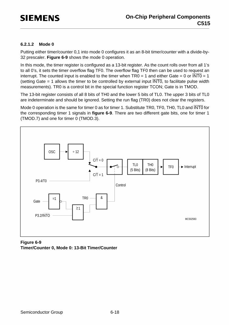
On-Chip Peripheral ComponentsC515
6.2.1.2 Mode 0
Putting either timer/counter 0,1 into mode 0 configures it as an 8-bit timer/counter with a divide-by-32 prescaler. Figure 6-9 shows the mode 0 operation.
In this mode, the timer register is configured as a 13-bit register. As the count rolls over from all 1’sto all 0’s, it sets the timer overflow flag TF0. The overflow flag TF0 then can be used to request aninterrupt. The counted input is enabled to the timer when TR0 = 1 and either Gate = 0 or INT0 = 1(setting Gate = 1 allows the timer to be controlled by external input INT0, to facilitate pulse widthmeasurements). TR0 is a control bit in the special function register TCON; Gate is in TMOD.
The 13-bit register consists of all 8 bits of TH0 and the lower 5 bits of TL0. The upper 3 bits of TL0are indeterminate and should be ignored. Setting the run flag (TR0) does not clear the registers.
Mode 0 operation is the same for timer 0 as for timer 1. Substitute TR0, TF0, TH0, TL0 and INT0 forthe corresponding timer 1 signals in figure 6-9 . There are two different gate bits, one for timer 1(TMOD.7) and one for timer 0 (TMOD.3).
Figure 6-9 Timer/Counter 0, Mode 0: 13-Bit Timer/Counter
MCS02583
1
&
OSC
C/T = 0TL0 TH0 TF0
C/T = 1
TR0Gate
P3.2/INTO
Control
Interrupt
P3.4/T0
(5
÷ 12
=1
Bits) Bits)(8
_<
Semiconductor Group 6-18

On-Chip Peripheral ComponentsC515
6.2.1.3 Mode 1
Mode 1 is the same as mode 0, except that the timer register is running with all 16 bits. Mode 1 isshown in figure 6-10 .
Figure 6-10 Timer/Counter 0, Mode 1: 16-Bit Timer/Counter
P3.2/INT0MCS02095
1
&
OSC
C/T = 0TL0 TH0 TF0
C/T = 1
(8 Bits)
TR0Gate
P3.2/INTO
Control
Interrupt
P3.4/T0
(8 Bits)
_<
÷ 12
=1
Semiconductor Group 6-19

On-Chip Peripheral ComponentsC515
6.2.1.4 Mode 2
Mode 2 configures the timer register as an 8-bit counter (TL0) with automatic reload, as shown infigure 6-11 . Overflow from TL0 not only sets TF0, but also reloads TL0 with the contents of TH0,which is preset by software. The reload leaves TH0 unchanged.
Figure 6-11 Timer/Counter 0,1, Mode 2: 8-Bit Timer/Counter with Auto-Reload
P3.2/INT0
Semiconductor Group 6-20
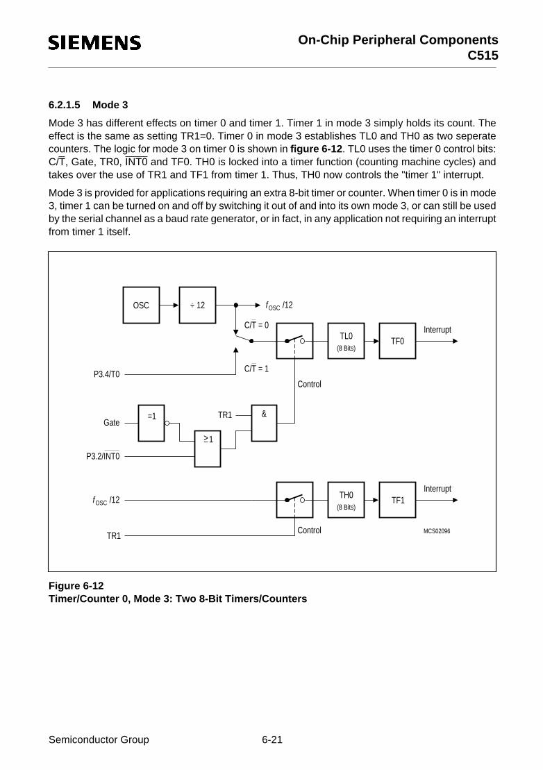
On-Chip Peripheral ComponentsC515
6.2.1.5 Mode 3
Mode 3 has different effects on timer 0 and timer 1. Timer 1 in mode 3 simply holds its count. Theeffect is the same as setting TR1=0. Timer 0 in mode 3 establishes TL0 and TH0 as two seperatecounters. The logic for mode 3 on timer 0 is shown in figure 6-12 . TL0 uses the timer 0 control bits:C/T, Gate, TR0, INT0 and TF0. TH0 is locked into a timer function (counting machine cycles) andtakes over the use of TR1 and TF1 from timer 1. Thus, TH0 now controls the "timer 1" interrupt.
Mode 3 is provided for applications requiring an extra 8-bit timer or counter. When timer 0 is in mode3, timer 1 can be turned on and off by switching it out of and into its own mode 3, or can still be usedby the serial channel as a baud rate generator, or in fact, in any application not requiring an interruptfrom timer 1 itself.
Figure 6-12 Timer/Counter 0, Mode 3: Two 8-Bit Timers/Counters
MCS02096
1
&
OSC
C/T = 0TL0 TF0
C/T = 1
(8 Bits)
TR1Gate
P3.2/INT0
Control
Interrupt
(8 Bits)
TH0Interrupt
TF1
ControlTR1
/12f OSC
OSCf /12
P3.4/T0
÷ 12
=1
<_
Semiconductor Group 6-21

On-Chip Peripheral ComponentsC515
6.2.2 Timer/Counter 2 with Additional Compare/Capture/Reload
The timer 2 with additional compare/capture/reload features is one of the most powerful peripheralunits of the C515. lt can be used for all kinds of digital signal generation and event capturing likepulse generation, pulse width modulation, pulse width measuring etc.
Timer 2 is designed to support various automotive control applications (ignition/injection-control,anti-lock-brake ... ) as well as industrial applications (DC-, three-phase AC- and stepper-motorcontrol, frequency generation, digital-to-analog conversion, process control ...). Please note thatthis timer is not equivalent to timer 2 of the C501.
The C515 timer 2 in combination with the compare/capture/reload registers allows the followingoperating modes:
– Compare : up to 4 PWM signals with 65535 steps at maximum and 500 ns resolution– Capture : up to 4 high speed capture inputs with 500 ns resolution– Reload : modulation of timer 2 cycle time
The block diagram in figure 6-13 shows the general configuration of timer 2 with the additionalcompare/capture/reload registers. The I/O pins which can used for timer 2 control are located asmultifunctional port functions at port 1 (see table 6-3 ).
Table 6-3 Alternate Port Functions of Timer 2
Pin Symbol Function
P1.0 / INT3 / CC0 Compare output / capture input for CRC register
P1.1 / INT4 / CC1 Compare output / capture input for CC register 1
P1.2 / INT5 / CC2 Compare output / capture input for CC register 2
P1.3 / INT6 / CC3 Compare output / capture input for CC register 3
P1.5 / T2EX External reload trigger input
P1.7 / T2 External count or gate input to timer 2
Semiconductor Group 6-22

On-Chip Peripheral ComponentsC515
Figure 6-13 Timer 2 Block Diagram
MCB03205
Comparator
CCL3/CCH3
Capture
Input/OutputControl
P1.0/INT3/CC0
CC1INT4/P1.1/
CC2INT5/P1.2/
CC3INT6/P1.2/
CCL2/CCH2
Comparator
CCL1/CCH1
Comparator
CRCL/CRCH
ComparatorBit16 16 Bit 16 Bit 16 Bit
OSC
÷ 12
÷ 24
f OSC
T2PS
Sync.P1.7/T2
T2EXP1.5/ Sync.
&
T2I1T2I0
Timer 2TH2TL2 TF2
Reload
EXEN2
Reload
1EXF2 InterruptRequest
Compare
_<
Semiconductor Group 6-23
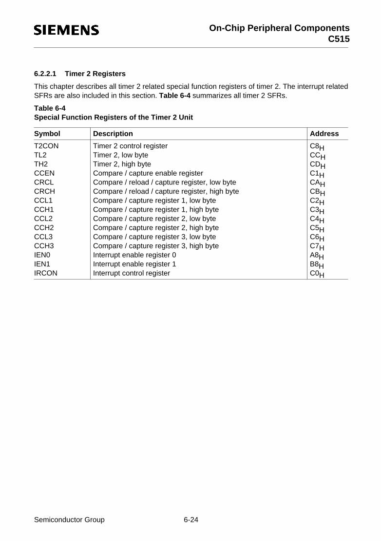
On-Chip Peripheral ComponentsC515
6.2.2.1 Timer 2 Registers
This chapter describes all timer 2 related special function registers of timer 2. The interrupt relatedSFRs are also included in this section. Table 6-4 summarizes all timer 2 SFRs.
Table 6-4 Special Function Registers of the Timer 2 Unit
Symbol Description Address
T2CONTL2TH2CCENCRCLCRCHCCL1CCH1CCL2CCH2CCL3CCH3IEN0IEN1IRCON
Timer 2 control registerTimer 2, low byteTimer 2, high byteCompare / capture enable registerCompare / reload / capture register, low byteCompare / reload / capture register, high byteCompare / capture register 1, low byteCompare / capture register 1, high byteCompare / capture register 2, low byteCompare / capture register 2, high byteCompare / capture register 3, low byteCompare / capture register 3, high byteInterrupt enable register 0Interrupt enable register 1Interrupt control register
C8HCCHCDHC1HCAHCBHC2HC3HC4HC5HC6HC7HA8HB8HC0H
Semiconductor Group 6-24

On-Chip Peripheral ComponentsC515
The T2CON timer 2 control register is a bitaddressable register which controls the timer 2 functionand the compare mode of registers CRC, CC1 to CC3.
Special Function Register T2CON (Address C8 H) Reset Value : 00 H
Bit Function
T2PS Prescaler select bitWhen set, timer 2 is clocked in the “timer“ or “gated timer“ function with 1/24 of theoscillator frequency. When cleared, timer 2 is clocked with 1/12 of the oscillatorfrequency. T2PS must be 0 for the counter operation of timer 2.
I3FR External interrupt 3 falling/rising edge flagUsed for capture function in combination with register CRC. lf set, a capture toregister CRC (if enabled) will occur on a positive transition at pin P1.0 / INT3 / CC0.lf I3FR is cleared, a capture will occur on a negative transition.
T2R1T2R0
Timer 2 reload mode selection
T2CM Compare mode bit for registers CRC, CC1 through CC3When set, compare mode 1 is selected. T2CM = 0 selects compare mode 0.
T2I1T2I0
Timer 2 input selection
CFH CEH CDH CCH CBH CAH C9H C8H
T2PS I3FR I2FR T2R1C8H T2CON
The shaded bit is not used in controlling timer/counter 2.
Bit No.7 6 5 4 3 2 1 0
MSB LSB
T2R0 T2CM T2I1 T2I0
T2R1 T2R0 Function
0 X Reload disabled
1 0 Mode 0 : auto-reload upon timer 2 overflow (TF2)
1 1 Mode 1 : reload on falling edge at pin P1.5 / T2EX.
T2I1 T2I0 Function
0 0 No input selected, timer 2 stops
0 1 Timer function : input frequency = fosc/12 (T2PS = 0) or fosc/24 (T2PS = 1)
1 0 Counter function : external input signal at pin P1.7 / T2
1 1 Gated timer function : input controlled by pin P1.7 / T2
Semiconductor Group 6-25

On-Chip Peripheral ComponentsC515
Special Function Register TL2 (Address CC H) Reset Value : 00 HSpecial Function Register TH2 (Address CD H) Reset Value : 00 HSpecial Function Register CRCL (Address CA H) Reset Value : 00 HSpecial Function Register CRCH (Address CB H) Reset Value : 00 H
Bit Function
TL2.7-0 Timer 2 value low byteThe TL2 register holds the 8-bit low part of the 16-bit timer 2 count value.
TH2.7-0 Timer 2 value high byteThe TH2 register holds the 8-bit high part of the 16-bit timer 2 count value.
CRCL.7-0 Compare / reload / capture register low byteCRCL is the 8-bit low byte of the 16-bit reload register of timer 2. It is also used forcompare/capture functions.
CRCH.7-0 Compare / reload / capture register high byteCRCH is the 8-bit high byte of the 16-bit reload register of timer 2. It is also used for compare/capture functions.
.7 .6 .5 .4CCH TL2
Bit No.7 6 5 4 3 2 1 0
MSB LSB
.3 .2 .1 LSB
MSB .6 .5 .4CDH TH2.3 .2 .1 .0
.7 .6 .5 .4CAH CRCL.3 .2 .1 LSB
MSB .6 .5 .4CBH CRCH.3 .2 .1 .0
Semiconductor Group 6-26
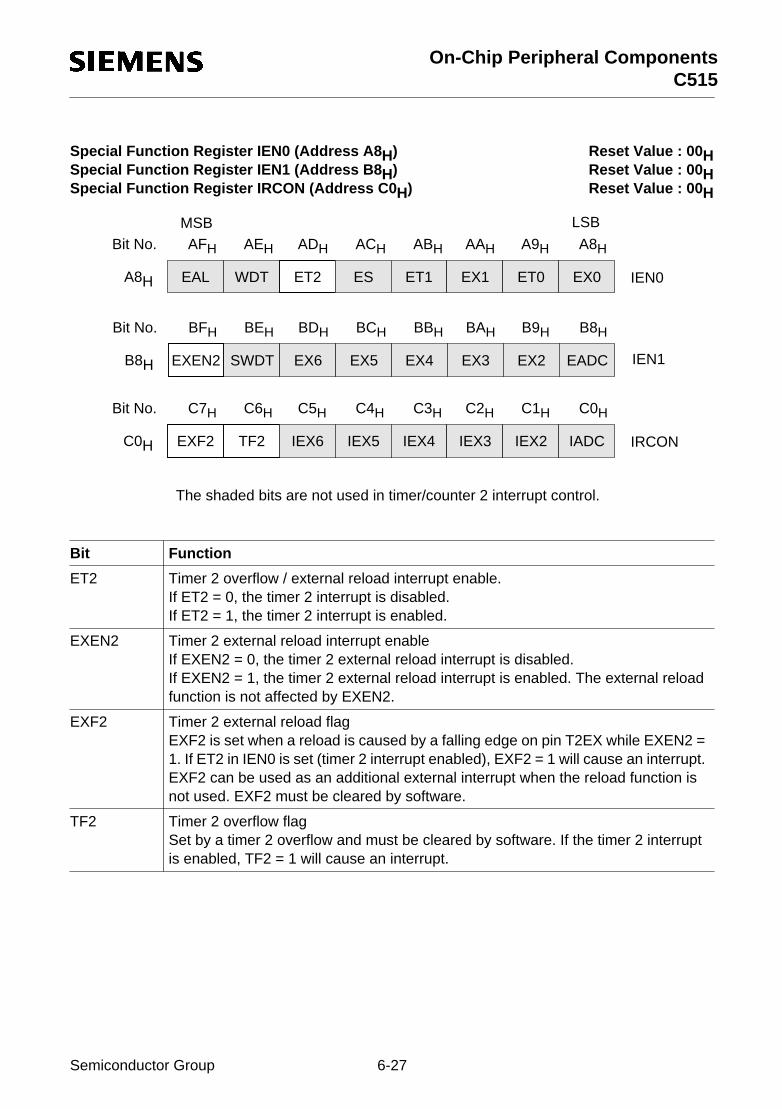
On-Chip Peripheral ComponentsC515
Special Function Register IEN0 (Address A8 H) Reset Value : 00 HSpecial Function Register IEN1 (Address B8 H) Reset Value : 00 HSpecial Function Register IRCON (Address C0 H) Reset Value : 00 H
Bit Function
ET2 Timer 2 overflow / external reload interrupt enable.If ET2 = 0, the timer 2 interrupt is disabled. If ET2 = 1, the timer 2 interrupt is enabled.
EXEN2 Timer 2 external reload interrupt enableIf EXEN2 = 0, the timer 2 external reload interrupt is disabled. If EXEN2 = 1, the timer 2 external reload interrupt is enabled. The external reload function is not affected by EXEN2.
EXF2 Timer 2 external reload flagEXF2 is set when a reload is caused by a falling edge on pin T2EX while EXEN2 = 1. If ET2 in IEN0 is set (timer 2 interrupt enabled), EXF2 = 1 will cause an interrupt. EXF2 can be used as an additional external interrupt when the reload function is not used. EXF2 must be cleared by software.
TF2 Timer 2 overflow flagSet by a timer 2 overflow and must be cleared by software. If the timer 2 interrupt is enabled, TF2 = 1 will cause an interrupt.
EXF2 TF2 IEX6 IEX5C0H IRCON
Bit No. C7H
IEX4 IEX3 IEX2 IADC
C6H C5H C4H C3H C2H C1H C0H
The shaded bits are not used in timer/counter 2 interrupt control.
EAL WDT ET2 ESA8H IEN0
Bit No. AFH
MSB LSB
ET1 EX1 ET0 EX0
AEH ADH ACH ABH AAH A9H A8H
EXEN2 SWDT EX6 EX5B8H IEN1
Bit No. BFH
EX4 EX3 EX2 EADC
BEH BDH BCH BBH BAH B9H B8H
Semiconductor Group 6-27

On-Chip Peripheral ComponentsC515
Special Function Register CCEN (Address C1 H) Reset Value : 00 H
Bit Function
COCAH3COCAL3
Compare/capture mode for CC register 3
COCAH2COCAL2
Compare/capture mode for CC register 2
COCAH1COCAL1
Compare/capture mode for CC register 1
COCAH0COCAL0
Compare/capture mode for CRC register
COCAH3 COCAL3 COCAH2 COCAL2C1H CCEN
Bit No.7 6 5 4 3 2 1 0
MSB LSB
COCAH1 COCAL1 COCAH0 COCAL0
COCAH3 COCAL3 Function
0 0 Compare/capture disabled
0 1 Capture on rising edge at pin P1.3 / INT6 / CC3
1 0 Compare enabled
1 1 Capture on write operation into register CCL3
COCAH2 COCAL2 Function
0 0 Compare/capture disabled
0 1 Capture on rising edge at pin P1.2 / INT5 / CC2
1 0 Compare enabled
1 1 Capture on write operation into register CCL2
COCAH1 COCAL1 Function
0 0 Compare/capture disabled
0 1 Capture on rising edge at pin P1.1 / INT4 / CC1
1 0 Compare enabled
1 1 Capture on write operation into register CCL1
COCAH0 COCAL0 Function
0 0 Compare/capture disabled
0 1 Capture on falling/rising edge at pin P1.0 / INT3 / CC0
1 0 Compare enabled
1 1 Capture on write operation into register CRCL
Semiconductor Group 6-28

On-Chip Peripheral ComponentsC515
6.2.2.2 Timer 2 Operation
The timer 2, which is a 16-bit-wide register, can operate as timer, event counter, or gated timer. Thedetailed operation is described below.
Timer Mode
In timer function, the count rate is derived from the oscillator frequency. A prescaler offers thepossibility of selecting a count rate of 1/12 or 1/24 of the oscillator frequency. Thus, the 16-bit timerregister (consisting of TH2 and TL2) is either incremented in every machine cycle or in every secondmachine cycle. The prescaler is selected by bit T2PS in special function register T2CON. lf T2PS iscleared, the input frequency is 1/12 of the oscillator frequency. if T2PS is set, the 2:1 prescaler gates1/24 of the oscillator frequency to the timer.
Gated Timer Mode
In gated timer function, the external input pin P1.7 / T2 functions as a gate to the input of timer 2. lfT2 is high, the internal clock input is gated to the timer. T2 = 0 stops the counting procedure. Thisfacilitates pulse width measurements. The external gate signal is sampled once every machinecycle.
Event Counter Mode
In the counter function, the timer 2 is incremented in response to a 1-to-0 transition at itscorresponding external input pin P1.7 / T2 In this function, the external input is sampled everymachine cycle. When the sampled inputs show a high in one cycle and a low in the next cycle, thecount is incremented. The new count value appears in the timer register in the cycle following theone in which the transition was detected. Since it takes two machine cycles (24 oscillator periods)to recognize a 1-to-0 transition, the maximum count rate is 1/24 of the oscillator frequency. Thereare no restrictions on the duty cycle of the external input signal, but to ensure that a given level issampled at least once before it changes, it must be held for at least one full machine cycle.
Note: The prescaler must be off for proper counter operation of timer 2, i.e. T2PS must be 0.
In either case, no matter whether timer 2 is configured as timer, event counter, or gated timer, arolling-over of the count from all 1’s to all 0’s sets the timer overflow flag TF2 in SFR IRCON, whichcan generate an interrupt.
lf TF2 is used to generate a timer overflow interrupt, the request flag must be cleared by the interruptservice routine as it could be necessary to check whether it was the TF2 flag or the external reloadrequest flag EXF2 which requested the interrupt. Both request flags cause the program to branch tothe same vector address.
Semiconductor Group 6-29

On-Chip Peripheral ComponentsC515
Reload of Timer 2
The reload mode for timer 2 is selected by bits T2R0 and T2R1 in SFR T2CON. Figure 6-14 showsthe configuration of timer 2 in reload mode.
Mode 0 : When timer 2 rolls over from all l’s to all 0’s, it not only sets TF2 but also causes the timer2 registers to be loaded with the 16-bit value in the CRC register, which is preset bysoftware. The reload will happen in the same machine cycle in which TF2 is set, thusoverwriting the count value 0000H.
Mode 1 : When a 16-bit reload from the CRC register is caused by a negative transition at thecorresponding input pin T2EX/P1.5. In addition, this transition will set flag EXF2, if bitEXEN2 in SFR IEN1 is set. lf the timer 2 interrupt is enabled, setting EXF2 will generatean interrupt. The external input pin T2EX is sampled in every machine cycle. When thesampling shows a high in one cycle and a low in the next cycle, a transition will berecognized. The reload of timer 2 registers will then take place in the cycle following theone in which the transition was detected.
Figure 6-14 Timer 2 in Reload Mode
MCS01903
1
Mode 1
EXF2
0Mode
EXEN2
TF2CRCHCRCL
Reload
TH2TL2InputClock
TimerInterruptRequest
T2EXP1.5
2<_
Semiconductor Group 6-30

On-Chip Peripheral ComponentsC515
6.2.2.3 Compare Function of Registers CRC, CC1 to CC3
The compare function of a timer/register combination can be described as follows. The 16-bit valuestored in a compare/capture register is compared with the contents of the timer register. lf the countvalue in the timer register matches the stored value, an appropriate output signal is generated at acorresponding port pin, and an interrupt is requested.
The contents of a compare register can be regarded as ’time stamp’ at which a dedicated outputreacts in a predefined way (either with a positive or negative transition). Variation of this ’time stamp’somehow changes the wave of a rectangular output signal at a port pin. This may - as a variationof the duty cycle of a periodic signal - be used for pulse width modulation as well as for a continuallycontrolled generation of any kind of square wave forms. Two compare modes are implemented tocover a wide range of possible applications.
The compare modes 0 and 1 are selected by bit T2CM in special function register T2CON. In bothcompare modes, the new value arrives at the port pin 1 within the same machine cycle in which theinternal compare signal is activated.
The four registers CRC, CC1 to CC3 are multifunctional as they additionally provide a capture,compare or reload capability (the CRC register only). A general selection of the function is done inregister CCEN. Please note that the compare interrupt CC0 can be programmed to be negative orpositive transition activated. The internal compare signal (not the output signal at the port pin!) isactive as long as the timer 2 contents is equal to the one of the appropriate compare registers, andit has a rising and a falling edge. Thus, when using the CRC register, it can be selected whether aninterrupt should be caused when the compare signal goes active or inactive, depending on bit I3FRin T2CON. For the CC registers 1 to 3 an interrupt is always requested when the compare signalgoes active (see figure 6-16 ).
6.2.2.3.1 Compare Mode 0
In mode 0, upon matching the timer and compare register contents, the output signal changes fromlow to high. lt goes back to a low level on timer overflow. As long as compare mode 0 is enabled,the appropriate output pin is controlled by the timer circuit only, and not by the user. Writing to theport will have no effect. Figure 6-15 shows a functional diagram of a port latch in compare mode 0.The port latch is directly controlled by the two signals timer overflow and compare. The input linefrom the internal bus and the write-to-latch line are disconnected when compare mode 0 is enabled.
Compare mode 0 is ideal for generating pulse width modulated output signals, which in turn can beused for digital-to-analog conversion via a filter network or by the controlled device itself (e.g. theinductance of a DC or AC motor). Mode 0 may also be used for providing output clocks with initiallydefined period and duty cycle. This is the mode which needs the least CPU time. Once set up, theoutput goes on oscillating without any CPU intervention. Figure 6-16 and 6-17 illustrate the functionof compare mode 0.
Semiconductor Group 6-31
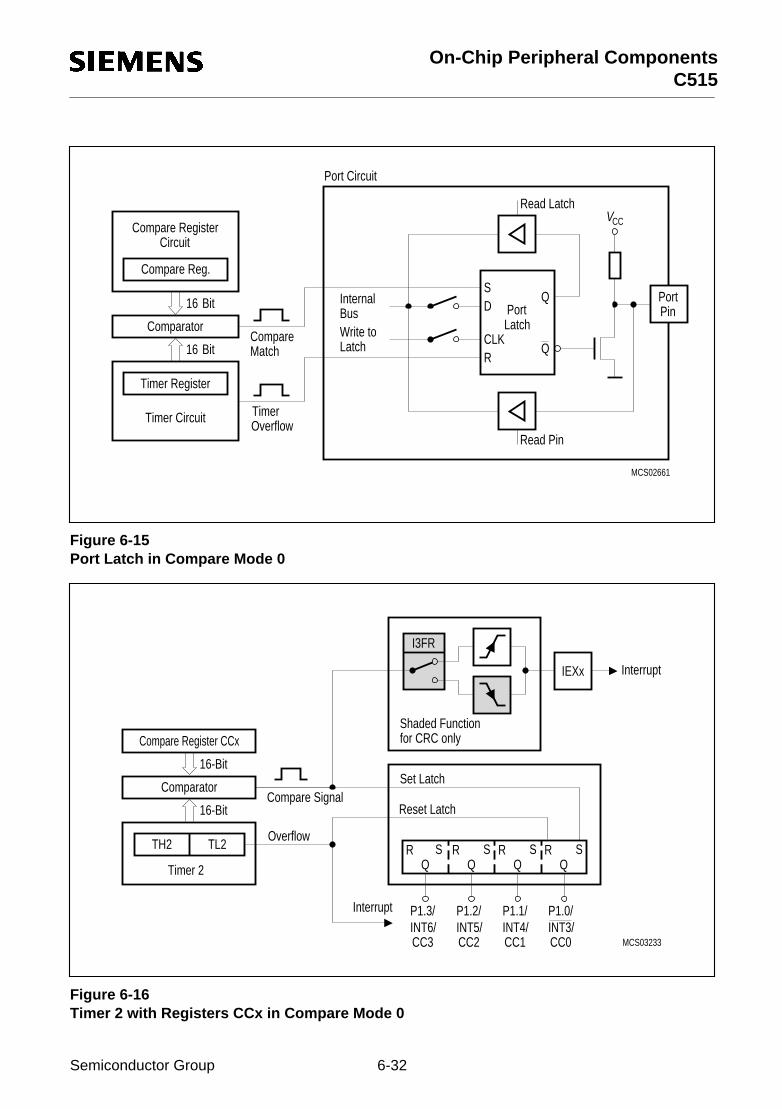
On-Chip Peripheral ComponentsC515
Figure 6-15 Port Latch in Compare Mode 0
Figure 6-16 Timer 2 with Registers CCx in Compare Mode 0
MCS02661
LatchPort
Q
QCLK
DPortPin
Read Pin
CCVRead Latch
Port Circuit
InternalBus
LatchWrite to
Compare Reg.
Compare RegisterCircuit
Comparator
Timer Register
Timer Circuit
CompareMatch
S
R
OverflowTimer
16 Bit
Bit16
MCS03233
IEXx
for CRC only
CC0INT3/P1.0/
Compare Signal
Overflow
Interrupt
Set Latch
Reset Latch
TL2
Timer 2
TH2
Comparator
Shaded Function
Interrupt
16-Bit
Compare Register CCx
P1.3/INT6/CC3
QR S SR
QSR
QSR
Q
CC2INT5/P1.2/ P1.1/
INT4/CC1
16-Bit
I3FR
Semiconductor Group 6-32

On-Chip Peripheral ComponentsC515
Figure 6-17 Function of Compare Mode 0
6.2.2.3.2 Modulation Range in Compare Mode 0
Generally it can be said that for every PWM generation in compare mode 0 with n-bit wide compareregisters there are 2n different settings for the duty cycle. Starting with a constant low level (0%dutycycle) as the first setting, the maximum possible duty cycle then would be :
(1 - 1/2n) x 100%
This means that a variation of the duty cycle from 0% to real 100% can never be reached if thecompare register and timer register have the same length. There is always a spike which is as longas the timer clock period.
This “spike“ may either appear when the compare register is set to the reload value (limiting thelower end of the modulation range) or it may occur at the end of a timer period. In a timer 2/CCxregister configuration in compare mode 0 this spike is divided into two halves: one at the beginningwhen the contents of the compare register is equal to the reload value of the timer; the other halfwhen the compare register is equal to the maximum value of the timer register (here: FFFFH).Please refer to figure 6-18 where the maximum and minimum duty cycle of a compare output signalis illustrated. Timer 2 is incremented with the machine clock (fosc/12), thus at 24-MHz operationalfrequency, these spikes are both approx. 250 ns long.
MCT01906
Timer Count = FFFF
Timer Count =Compare Value
ContentsofTimer 2
Timer Count = Reload Value
Interrupt can be generatedon overflow
CompareOutput(P1.x/CCx)
Interrupt can be generatedon compare-match
~~ ~ ~
H
Semiconductor Group 6-33

On-Chip Peripheral ComponentsC515
Figure 6-18 Modulation Range of a PWM Signal, generated with a Timer 2/CCx Register Combination inCompare Mode 0*
The following example shows how to calculate the modulation range for a PWM signal. To calculatewith reasonable numbers, a reduction of the resolution to 8-bit is used. Otherwise (for the maximumresolution of 16-bit) the modulation range would be so severely limited that it would be negligible.
Example:
Timer 2 in auto-reload mode; contents of reload register CRC = FF00H
Restriction of modulation range = 1 / 256 x 2 x 100% = 0.195%
This leads to a variation of the duty cycle from 0.195% to 99.805% for a timer 2/CCx registerconfiguration when 8 of 16 bits are used.
MCT01907
H
L
P1.x
CCHx/CCLx = 0000 or = CRCH/CRCL (maximum duty cycle)
P1.x
L
H
CCHx/CCLx = FFFF (minimum duty cycle)
Appr. 1/2 Machine Cycle
a)
b)
Appr. 1/2 Machine Cycle
H
H
Semiconductor Group 6-34

On-Chip Peripheral ComponentsC515
6.2.2.3.3 Compare Mode 1
In compare mode 1, the software adaptively determines the transition of the output signal. lt iscommonly used when output signals are not related to a constant signal perlod (as in a standardPWM Generation) but must be controlled very precisely with high resolution and without jitter. Incompare mode 1, both transitions of a signal can be controlled. Compare outputs in this mode canbe regarded as high speed outputs which are independent of the CPU activity.
lf compare mode 1 is enabled and the software writes to the appropriate output latch at the port, thenew value will not appear at the output pin until the next compare match occurs. Thus, one canchoose whether the output signal is to make a new transition (1-to-0 or 0-to-1, depending on theactual pinlevel) or should keep its old value at the time the timer 2 count matches the storedcompare value.
Figure 6-19 and figure 6-20 show functional diagrams of the timer/compare register/port latchconfiguration in compare mode 1. In this function, the port latch consists of two separate latches.The upper latch (which acts as a “shadow latch“) can be written under software control, but its valuewill only be transferred to the output latch (and thus to the port pin) in response to a compare match.
Note that the double latch structure is transparent as long as the internal compare signal is active.While the compare signal is active, a write operation to the port will then change both latches. Thismay become important when driving timer 2 with a slow external clock. In this case the comparesignal could be active for many machine cycles in which the CPU could unintentionally change thecontents of the port latch.
A read-modify-write instruction will read the user-controlled „shadow latch“ and write the modifiedvalue back to this “shadow-latch“. A standard read instruction will - as usual - read the pin of thecorresponding compare output.
Semiconductor Group 6-35

On-Chip Peripheral ComponentsC515
Figure 6-19 Port Latch in Compare Mode 1
Figure 6-20 Timer 2 with Registers CCx in Compare Mode 1
(CCx stands for CRC, CC1 to CC3, IEXx stands for IEX3 to IEX6)
MCS02662
LatchPort
Q
QCLK
D
Read Pin
CCV
D
CLK
QShadowLatch
Read Latch
Port Circuit
InternalBus
LatchWrite to
Compare Reg.
Compare RegisterCircuit
Comparator
Timer Register
Timer Circuit
CompareMatch
PinPort16 Bit
16 Bit
MCS02732
IEXx
for CRC only
P1.7
CC0INT3/P1.0/
Compare Signal
OverflowInterrupt
Output Latch
Shadow LatchPortLatchCircuit
2
TL2
Timer
TH2
Comparator
Shaded Function
Interrupt
16 Bit
16 Bit
Compare Register CCx
P1.3/INT6/CC3
I3FR
Semiconductor Group 6-36
On-Chip Peripheral ComponentsC515
6.2.2.4 Using Interrupts in Combination with the Compare Function
The compare service of registers CRC, CC1, CC2 and CC3 is assigned to alternate output functionsat port pins P1.0 to P1.3. Another option of these pins is that they can be used as external interruptinputs. However, when using the port lines as compare outputs then the input line from the port pinto the interrupt system is disconnected (but the pin’s level can still be read under software control).Thus, a change of the pin’s level will not cause a setting of the corresponding interrupt flag. In thiscase, the interrupt input is directly connected to the (internal) compare signal thus providing acompare interrupt.
The compare interrupt can be used very effectively to change the contents of the compare registersor to determine the level of the port outputs for the next “compare match“. The principle is, that theinternal compare signal (generated at a match between timer count and register contents) not onlymanipulates the compare output but also sets the corresponding interrupt request flag. Thus, thecurrent task of the CPU is interrupted - of course provided the priority of the compare interrupt ishigher than the present task priority - and the corresponding interrupt service routine is called. Thisservice routine then sets up all the necessary parameters for the next compare event.
Advantages when using compare interrupts
Firstly, there is no danger of unintentional overwriting a compare register before a match has beenreached. This could happen when the CPU writes to the compare register without knowing aboutthe actual timer 2 count.
Secondly, and this is the most interesting advantage of the compare feature, the output pin isexclusively controlled by hardware therefore completely independent from any service delay whichin real time applications could be disastrous. The compare interrupt in turn is not sensitive to suchdelays since it loads the parameters for the next event. This in turn is supposed to happen after asuff icient space of time.
Please note two special cases where a program using compare interrupts could show a “surprising“behavior :
The first configuration has already been mentioned in the description of compare mode 1. The factthat the compare interrupts are transition activated becomes important when driving timer 2 with aslow external clock. In this case it should be carefully considered that the compare signal is activeas long as the timer 2 count is equal to the contents of the corresponding compare register, and thatthe compare signal has a rising and a falling edge. Furthermore, the “shadow latches“ used incompare mode 1 are transparent while the compare signal is active.
Thus, with a slow input clock for timer 2, the comparator signal is active for a long time (= highnumber of machine cycles) and therefore a fast interrupt controlled reload of the compare registercould not only change the “shadow latch“ - as probably intended - but also the output buffer.
When using the CRC, you can select whether an interrupt should be generated when the comparesignal goes active or inactive, depending on the status of bit I3FR in T2CON.
Initializing the interrupt to be negative transition triggered is advisable in the above case. Then thecompare signal is already inactive and any write access to the port latch just changes the contentsof the “shadow-latch“.
Please note that for CC registers 1 to 3 an interrupt is always requested when the compare signalgoes active.
Semiconductor Group 6-37

On-Chip Peripheral ComponentsC515
The second configuration which should be noted is when compare function is combined withnegative transition activated interrupts. lf the port latch of port P1.0 contains a 1, the interruptrequest flags IEX3 will immediately be set after enabling the compare mode for the CRC register.The reason is that first the external interrupt input is controlled by the pin’s level. When the compareoption is enabled the interrupt logic input is switched to the internal compare signal, which carriesa low level when no true comparison is detected. So the interrupt logic sees a 1-to-0 edge and setsthe interrupt request flag.
An unintentional generation of an interrupt during compare initialization can be prevented lf therequest flag is cleared by software after the compare is activated and before the external interruptis enabled.
Semiconductor Group 6-38

On-Chip Peripheral ComponentsC515
6.2.2.5 Capture Function
Each of the compare/capture registers CC1 to CC3 and the CRC register can be used to latch thecurrent 16-bit value of the timer 2 registers TL2 and TH2. Two different modes are provided for thisfunction. In mode 0, an external event latches the timer 2 contents to a dedicated capture register.In mode 1, a capture will occur upon writing to the low order byte of the dedicated 16-bit captureregister. This mode is provided to allow the software to read the timer 2 contents “on-the-fly“.
In mode 0, the external event causing a capture is :
– for CC registers 1 to 3: a positive transition at pins CC1 to CC3 of port 1– for the CRC register: a positive or negative transition at the corresponding pin, depending
on the status of the bit I3FR in SFR T2CON. lf the edge flag iscleared, a capture occurs in response to a negative transition; lf theedge flag is set a capture occurs in response to a positive transitionat pin P1.0 / INT3 / CC0.
In both cases the appropriate port 1 pin is used as input and the port latch must be programmed tocontain a one (1). The external input is sampled in every machine cycle. When the sampled inputshows a low (high) level in one cycle and a high (low) in the next cycle, a transition is recognized.The timer 2 contents is latched to the appropriate capture register in the cycle following the one inwhich the transition was identified.
In mode 0 a transition at the external capture inputs of registers CC1 to CC3 will also set thecorresponding external interrupt request flags IEX3 to IEX6. lf the interrupts are enabled, anexternal capture signal will cause the CPU to vector to the appropriate interrupt service routine.
In mode 1 a capture occurs in response to a write instruction to the low order byte of a captureregister. The write-to-register signal (e.g. write-to-CRCL) is used to initiate a capture. The valuewritten to the dedicated capture register is irrelevant for this function. The timer 2 contents will belatched into the appropriate capture register in the cycle following the write instruction. In this modeno interrupt request will be generated.
Figure 6-21 illustrates the operation of the CRC register, while figure 6-22 shows the operation ofthe compare/capture registers 1 to 3.
The two capture modes can be established individually for each capture register by bits in SFRCCEN (compare/capture enable register). That means, in contrast to the compare modes, it ispossible to simultaneously select mode 0 for one capture register and mode 1 for another register.
Semiconductor Group 6-39

On-Chip Peripheral ComponentsC515
Figure 6-21 Timer 2 - Capture with Register CRC
Figure 6-22 Timer 2 - Capture with Registers CC1 to CC3
MCS01909
Mode 1
IEX3
0Mode
TF2
CRCHCRCL
Capture
TH2TL2Input
Clock
ExternalInterruptRequest
Timer 2InterruptRequest
3
T2CON.6
CRCL""Write to
CC03/P1.0/INT
MCS01910
Mode 1
IEX4
0Mode
TF2
CCH1CCL1
Capture
TH2TL2InputClock
ExternalInterrupt 4Request
Timer 2InterruptRequest
CCL1""Write to
CC14/P1.1/INT
Semiconductor Group 6-40

On-Chip Peripheral ComponentsC515
6.3 Serial Interface
The serial port of the C515 is full duplex, meaning it can transmit and receive simultaneously. It isalso receive-buffered, meaning it can commence reception of a second byte before a previouslyreceived byte has been read from the receive register (however, if the first byte still hasn’t been readby the time reception of the second byte is complete, one of the bytes will be lost). The serial portreceive and transmit registers are both accessed at special function register SBUF. Writing to SBUFloads the transmit register, and reading SBUF accesses a physically separate receive register.
The serial port can operate in 4 modes (one synchronous mode, three asynchronous modes). Thebaud rate clock for the serial port is derived from the oscillator frequency (mode 0, 2) or generatedeither by timer 1 or by a dedicated baud rate generator (mode 1, 3).
Mode 0, Shift Register (Synchronous) Mode:
Serial data enters and exits through RxD. TxD outputs the shift clock. 8 data bits are transmitted/received: (LSB first). The baud rate is fixed at 1/12 of the oscillator frequency. (See section 6.3.4 formore detailed information)
Mode 1, 8-Bit UART, Variable Baud Rate:
10 bits are transmitted (through TXD) or received (through RXD): a start bit (0), 8 data bits (LSBfirst), and a stop bit (1). On receive, the stop bit goes into RB8 in special function register SCON.The baud rate is variable. (See section 6.3.5 for more detailed information)
Mode 2, 9-Bit UART, Fixed Baud Rate:
11 bits are transmitted (through TXD) or received (through RXD): a start bit (0), 8 data bits (LSBfirst), a programmable 9th bit, and a stop bit (1). On transmit, the 9th data bit (TB8 in SCON) can beassigned to the value of 0 or 1. Or, for example, the parity bit (P, in the PSW) could be moved intoTB8. On receive, the 9th data bit goes into RB8 in special function register SCON, while the stop bitis ignored. The baud rate is programmable to either 1/32 or 1/64 of the oscillator frequency. (Seesection 6.3.6 for more detailed information)
Mode 3, 9-Bit UART, Variable Baud Rate:
11 bits are transmitted (through TXD) or received (through RXD): a start bit (0), 8 data bits (LSBfirst), a programmable 9th data bit, and a stop bit (1). In fact, mode 3 is the same as mode 2 in allrespects except the baud rate. The baud rate in mode 3 is variable. (See section 6.3.6 for moredetailed information)
In all four modes, transmission is initiated by any instruction that uses SBUF as a destinationregister. Reception is initiated in mode 0 by the condition RI = 0 and REN = 1. Reception is initiatedin the other modes by the incoming start bit if REN = 1. The serial interfaces also provide interruptrequests when a transmission or a reception of a frame has completed. The corresponding interruptrequest flags for serial interface 0 are TI or RI, resp. See chapter 7 of this user manual for moredetails about the interrupt structure. The interrupt request flags TI and RI can also be used forpolling the serial interface 0 if the serial interrupt is not to be used (i.e. serial interrupt 0 not enabled).
Semiconductor Group 6-41

On-Chip Peripheral ComponentsC515
6.3.1 Multiprocessor Communication
Modes 2 and 3 have a special provision for multiprocessor communications. In these modes, 9 databits are received. The 9th one goes into RB8. Then a stop bit follows. The port can be programmedsuch that when the stop bit is received, the serial port interrupt will be activated only if RB8 = 1. Thisfeature is enabled by setting bit SM2 in SCON. A way to use this feature in multiprocessor systemsis as follows.
When the master processor wants to transmit a block of data to one of several slaves, it first sendsout an address byte which identifies the target slave. An address byte differs from a data byte inthat the 9th bit is 1 in an address byte and 0 in a data byte. With SM2 = 1, no slave will be interruptedby a data byte. An address byte, however, will interrupt all slaves, so that each slave can examinethe received byte and see if it is beeing addressed. The addressed slave will clear its SM2 bit andprepare to receive the data bytes that will be coming. The slaves that weren't being addressed leavetheir SM2s set and go on about their business, ignoring the incoming data bytes.
SM2 has no effect in mode 0. SM2 can be used in mode 1 to check the validity of the stop bit. In amode 1 reception, if SM2 = 1, the receive interrupt will not be activated unless a valid stop bit isreceived.
6.3.2 Serial Port Registers
The serial port control and status register is the special function register SCON. This registercontains not only the mode selection bits, but also the 9th data bit for transmit and receive (TB8 andRB8), and the serial port interrupt bits (TI and RI).
SBUF is the receive and transmit buffer of serial interface 0. Writing to SBUF loads the transmitregister and initiates transmission. Reading out SBUF accesses a physically separate receiveregister.
Semiconductor Group 6-42

On-Chip Peripheral ComponentsC515
Special Function Register SCON (Address 98 H) Reset Value : 00 HSpecial Function Register SBUF (Address 99 H) Reset Value : XX H
Bit Function
SM0SM1
Serial port 0 operating mode selection bits
SM2 Enable serial port multiprocessor communication in modes 2 and 3In mode 2 or 3, if SM2 is set to 1 then RI0 will not be activated if the received 9th data bit (RB8) is 0. In mode 1, if SM2 = 1 then RI will not be activated if a valid stop bit was not received. In mode 0, SM2 should be 0.
REN Serial port receiver enableEnables serial reception. Set by software to enable serial reception. Cleared by software to disable serial reception.
TB8 Serial port transmitter bit 9TB8 is the 9th data bit that will be transmitted in modes 2 and 3. Set or cleared by software as desired.
RB8 Serial port receiver bit 9In modes 2 and 3, RB8 is the 9th data bit that was received. In mode 1, if SM2 = 0, RB8 is the stop bit that was received. In mode 0, RB8 is not used.
TI Serial port transmitter interrupt flagTI is set by hardware at the end of the 8th bit time in mode 0, or at the beginning of the stop bit in the other modes, in any serial transmission. TI must be cleared by software.
RI Serial port receiver interrupt flagRI is set by hardware at the end of the 8th bit time in mode 0, or halfway through the stop bit time in the other modes, in any serial reception (exception see SM2). RI must be cleared by software.
9FH 9EH 9DH 9CH 9BH 9AH 99H 98H
SM0 SM1 SM2 REN98H SCON
Bit No. MSB LSB
TB8 RB8 TI RI
99H SBUF
7 6 5 4 3 2 1 0
Serial Interface Buffer Register
SM0 SM1 Selected operating mode
0 0 Serial mode 0 : Shift register, fixed baud rate (fOSC/12)
0 1 Serial mode 1 : 8-bit UART, variable baud rate
1 0 Serial mode 2 : 9-bit UART, fixed baud rate (fOSC/32 or fOSC/64)
1 1 Serial mode 3 : 9-bit UART, variable baud rate
Semiconductor Group 6-43

On-Chip Peripheral ComponentsC515
6.3.3 Baud Rate Generation
There are several possibilities to generate the baud rate clock for the serial port depending on themode in which it is operating.
For clarification some terms regarding the difference between "baud rate clock" and "baud rate"should be mentioned. The serial interface requires a clock rate which is 16 times the baud rate forinternal synchronization. Therefore, the baud rate generators have to provide a "baud rate clock" tothe serial interface which - there divided by 16 - results in the actual "baud rate". However, allformulas given in the following section already include the factor and calculate the final baud rate.Further, the abrevation fOSC refers to the external clock frequency (oscillator or external input clockoperation).
The baud rate of the serial port is controlled by two bits which are located in the special functionregisters as shown below.
Special Function Register ADCON (Address D8 H) Reset Value : 00X00000 BSpecial Function Register PCON (Address 87 H) Reset Value : 000X0000 B
Figure 6-23 shows the configuration for the baud rate generation of the serial port.
Bit Function
BD Baud rate generator enableWhen set, the baud rate of serial interface 0 is derived from a dedicated prescaler. When cleared (default after reset), baud rate is derived from the timer 1 overflow rate.
SMOD Double baud rateWhen set, the baud rate of the serial interface in modes 1, 2, and 3 is doubled. After reset this bit is cleared.
SMOD PDS IDLS SD1)87H PCON
Bit No. MSB LSB
GF1 GF0 PDE IDLE
7 6 5 4 3 2 1 0
The shaded bits are not used in controlling the serial port baud rate.
BD CLK – BSYD8H ADCONADM MX2 MX1 MX0
DFH DEH DDH DCH DBH DAH D9H D8H
1) This bit is available for C515-LM/1RM versions only.
Semiconductor Group 6-44

On-Chip Peripheral ComponentsC515
Figure 6-23 Baud Rate Generation for the Serial Port
Depending on the programmed operating mode different paths are selected for the baud rate clockgeneration. Figure 6-23 shows the dependencies of the serial port 0 baud rate clock generationfrom the two control bits and from the mode which is selected in the special function register SCON.
6.3.3.1 Baud Rate in Mode 0
The baud rate in mode 0 is fixed to :
6.3.3.2 Baud Rate in Mode 2
The baud rate in mode 2 depends on the value of bit SMOD in special function register PCON. IfSMOD = 0 (which is the value after reset), the baud rate is 1/64 of the oscillator frequency. If SMOD= 1, the baud rate is 1/32 of the oscillator frequency.
MCB03206
Rate
f OSC
(SMOD)
Baud
Clock
PCON.7
÷ 2
(SM0/SM1)
SCON.7SCON.6
Only one modecan be selected
ADCON.7(BD)
01
01
Timer
Mode
Mode
Note: The switch configuration shows the reset state.
1
0
2
3ModeMode 1
Overflow
÷ 6
/2÷ 39
Mode 0 baud rate =oscillator frequency
12
Mode 2 baud rate = oscillator frequency64
2 SMOD
x
Semiconductor Group 6-45

On-Chip Peripheral ComponentsC515
6.3.3.3 Baud Rate in Mode 1 and 3
In these modes the baud rate is variable and can be generated alternatively by a baud rategenerator with a fixed prescaler or by timer 1.
6.3.3.3.1 Using the Baud Rate Generator
In modes 1 and 3, the C515 can use the internal baud rate generator for the serial port. To enablethis feature, bit BD (bit 7 of special function register ADCON) must be set. This baud rate generatordivides the oscillator frequency by 2 x 39=78. Bit SMOD (PCON.7) also can be used to enable adivide by 2 prescaler. For baud rate calculation the baud rate clock must be further divided by 16.Therefore, at 12 MHz oscillator frequency, the commonly used baud rates 4800 baud (SMOD=0)and 9600 (SMOD=1) are available (with 0.16 % deviation). The baud rate is determined by SMODand the oscillator frequency as follows :
6.3.3.3.2 Using Timer 1 to Generate Baud Rates
In mode 1 and 3 of the serial port also timer 1 can be used for generating baud rates. To enable thisfeature, bit BD (bit 7 of special function register ADCON) must be reset.Then the baud rate isdetermined by the timer 1 overflow rate and the value of SMOD as follows :
The timer 1 interrupt is usually disabled in this application. Timer 1 itself can be configured for either"timer" or "counter" operation, and in any of its operating modes. In most typical applications, it isconfigured for "timer" operation in the auto-reload mode (high nibble of TMOD = 0010B). In thiscase the baud rate is given by the formula:
Very low baud rates can be achieved with timer 1 if leaving the timer 1 interrupt enabled,configuring the timer to run as 16-bit timer (high nibble of TMOD = 0001B), and using the timer 1interrupt for a 16-bit software reload.
Table 6-5 lists various commonly used baud rates of the different modes. It also shows how thesebaud rates can be obtained using timer 1 in mode 1 or 3.
Mode 1,3 baud rate = oscillator frequency2496
2 SMOD
x
Mode 1, 3 baud rate = (timer 1 overflow rate)32
2SMOD
x
Mode 1, 3 baud rate =32 x 12 x (256 – (TH1))
2SMOD x oscillator frequency
Semiconductor Group 6-46

On-Chip Peripheral ComponentsC515
Table 6-5 Timer 1 generated Commonly used Baud Rates
Baud Rate fOSC (MHz) SMOD BD Timer 1
Mode Reload Value
Mode 1, 3: 62.5 Kbaud125 Kbaud19.5 Kbaud
9.6 Kbaud4.8 Kbaud2.4 Kbaud1.2 Kbaud110 Baud110 Baud4.8 Kbaud9.6 Kbaud6.4 Kbaud
12.8 Kbaud9.6 Kbaud
19.2 Kbaud
12.024.011.05911.05911.05911.05911.0596.012.012.012.016.016.024.024.0
111000000010101
000000000111111
222222221------
FFHFFHFDHFDHFAHF4HE8H72HFEEBH------
Mode 0 : 1 Mbaud1.33 Mbaud
2 Mbaud
12.016.024.0
---
---
---
---
Mode 2 : 187.5 Kbaud375 Kbaud250 Kbaud500 Kbaud375 Kbaud750 Kbaud
12.012.016.016.024.024.0
010101
------
------
------
Semiconductor Group 6-47

On-Chip Peripheral ComponentsC515
6.3.4 Details about Mode 0
Serial data enters and exists through RXD. TXD outputs the shift clock. 8 data bits are transmitted/received: (LSB first). The baud rate is fixed at fOSC/12.
Figure 6-24 shows a simplified functional diagram of the serial port in mode 0. The associatedtiming is illustrated in figure 6-25 .
Transmission is initiated by any instruction that uses SBUF as a destination register. The "Write-to-SBUF" signal at S6P2 also loads a 1 into the 9th position of the transmit shift register and tells theTX control block to commence a transmission. The internal timing is such that one full machinecycle will elapse between "Write-to-SBUF", and activation of SEND.
SEND enables the output of the shift register to the alternate output function line of P3.0, and alsoenables SHIFT CLOCK to the alternate output function line of P3.1. SHIFT CLOCK is low duringS3, S4, and S5 of every machine cycle, and high during S6, S1 and S2. At S6P2 of every machinecycle in which SEND is active, the contents of the transmit shift register are shifted one position tothe right.
As data bits shift out to the right, zeroes come in from the left. When the MSB of the data byte is atthe output position of the shift register, then the1 that was initially loaded into the 9th position, is justleft of the MSB, and all positions to the left of that contain zeroes. This condition flags the TX controlblock to do one last shift and then deactivate SEND and set TI. Both of these actions occur at S1P1of the 10th machine cycle after "Write-to-SBUF".
Reception is initiated by the condition REN = 1 and RI = 0. At S6P2 of the next machine cycle, theRX control unit writes the bits 1111 1110 to the receive shift register, and in the next clock phaseactivates RECEIVE.
RECEIVE enables SHIFT CLOCK to the alternate output function line of P3.1. SHIFT CLOCKmakes transitions at S3P1 and S6P1 of every machine cycle. At S6P2 of every machine cycle inwhich RECEIVE is active, the contents of the receive shift register are shifted one position to theleft. The value that comes in from the right is the value that was sampled at the P3.0 pin at S5P2 ofthe same machine cycle.
As data bit comes in from the right, 1’s shift out to the left. When the 0 that was initially loaded intothe rightmost position arrives at the leftmost position in the shift register, it flags the RX control blockto do one last shift and load SBUF. At S1P1 of the 10th machine cycle after the write to SCON thatcleared RI, RECEIVE is cleared and RI is set.
Semiconductor Group 6-48

On-Chip Peripheral ComponentsC515
Figure 6-24 Serial Interface, Mode 0, Functional Diagram
MCS02101
Internal Bus
1
SBUF
Zero Detector
D
S
CLK
Q
Shift
Send
1
TX Control
Start
TX Clock TI
RX Control
Start RI Receive
Shift
SerialPort
Interrupt
Input Shift Register
SBUF
Internal Bus
Writeto
SBUF
ShiftLoadSBUF
ReadSBUF
RXDP3.0 Alt.OutputFunction
FunctionOutputP3.1 Alt.TXD1
ShiftClock
&
REN
RI
S6
RX Clock
FunctionInputP3.0 Alt.RXD
01 1 1 1 1 1 1
&
&
Shift
BaudRateClock
_<
_<
Baud Rate Clock
Semiconductor Group 6-49

On-Chip Peripheral ComponentsC515
Figure 6-25 Serial Interface, Mode 0, Timing Diagram
S 12S
3S4S
5S6S
S 6S 5
S 4S 3
S 21S
S 6S 5
S 4S 3
S 21S
S 6S 5
S 4S 3
S 21S
S 6S 5
S 4S 3
S 21S
S 6S 5
S 4S 3
S 21S
S 6S 5
S 4S 3
S 21S
S 6S 5
S 4S 3
S 21S
S 6S 5
S 4S 3
S 21S
S 6S 5
S 4S 3
S 21S
D0D1
D2D3
D4D5
D6D7
ALE
Writ
e to
SBU
F
Send
Shift
RXD
(Dat
a O
ut)
S6P2
TXD
(Shi
ft Cl
ock)
S3P1
S6P1
Writ
e to
SCO
N (C
lear
RI)
Shift
Rece
ive
RI RXD
(Dat
a In
)
TXD
(Shi
ft Cl
ock)
D0D1
D2D3
D4D5
D6D7
S5P
TI
MCT
0210
2
ReceiveTransmit
Semiconductor Group 6-50

On-Chip Peripheral ComponentsC515
6.3.5 Details about Mode 1
Ten bits are transmitted (through TXD), or received (through RXD): a start bit (0), 8 data bits (LSBfirst), and a stop bit (1). On receive, the stop bit goes into RB8 in SCON. The baud rate isdetermined either by the timer 1 overflow rate or by the internal baud rate generator.
Figure 6-26 shows a simplified functional diagram of the serial port in mode 1. The associatedtimings for transmit/receive are illustrated in figure 6-27 .
Transmission is initiated by an instruction that uses SBUF as a destination register. The "Write-to-SBUF" signal also loads a 1 into the 9th bit position of the transmit shift register and flags the TXcontrol unit that a transmission is requested. Transmission starts at the next rollover in the divide-by-16 counter. (Thus, the bit times are synchronized to the divide-by-16 counter, not to the "Write-to-SBUF" signal).
The transmission begins with activation of SEND, which puts the start bit at TXD. One bit time later,DATA is activated, which enables the output bit of the transmit shift register to TXD. The first shiftpulse occurs one bit time after that.
As data bits shift out to the right, zeroes are clocked in from the left. When the MSB of the data byteis at the output position of the shift register, then the 1 that was initially loaded into the 9th positionis just to the left of the MSB, and all positions to the left of that contain zeroes. This condition flagsthe TX control unit to do one last shift and then deactivate SEND and set TI. This occurs at the 10thdivide-by-16 rollover after "Write-to-SBUF".
Reception is initiated by a detected 1-to-0 transition at RXD. For this purpose RXD is sampled at arate of 16 times whatever baud rate has been established. When a transition is detected, the divide-by-16 counter is immediately reset, and 1FFH is written into the input shift register, and receptionof the rest of the frame will proceed.
The 16 states of the counter divide each bit time into 16ths. At the 7th, 8th and 9th counter statesof each bit time, the bit detector samples the value of RXD. The value accepted is the value thatwas seen in at latest 2 of the 3 samples. This is done for the noise rejection. If the value acceptedduring the first bit time is not 0, the receive circuits are reset and the unit goes back to looking foranother 1-to-0 transition. This is to provide rejection or false start bits. If the start bit proves valid, itis shifted into the input shift register, and reception of the rest of the frame will proceed.
As data bits come in from the right, 1s shift out to the left. When the start bit arrives at the leftmostposition in the shift register, (which in mode 1 is a 9-bit register), it flags the RX control block to doone last shift, load SBUF and RB8, and set RI. The signal to load SBUF and RB8, and to set RI, willbe generated if, and only if, the following conditions are met at the time the final shift pulse isgenerated.
1) RI = 0, and2) either SM2 = 0, or the received stop bit = 1
If one of these two condtions is not met, the received frame is irretrievably lost. If both conditionsare met, the stop bit goes into RB8, the 8 data bit goes into SBUF, and RI is activated. At this time,whether the above conditions are met or not, the unit goes back to looking for a 1-to-0 transition inRXD.
Semiconductor Group 6-51

On-Chip Peripheral ComponentsC515
Figure 6-26 Serial Interface, Mode 1, Functional Diagram
MCS02103
Internal Bus
1
SBUF
Zero Detector
D
S
CLK
Q
Data
Send
1-to-0TransitionDetector
TX Control
ShiftStart
TX Clock
RX ControlStart
Load
Shift
SBUF
Sample
BitDetector
(9Bits)Input Shift Register
1FF
SBUF
Internal Bus
Writeto
SBUF
TXD
BaudRateClock
RXDShift
LoadSBUF
ReadSBUF
1&
÷ 16
÷ 16
RX
InterruptPort
Serial 1
TI
RI
H
_<
_<
Semiconductor Group 6-52

On-Chip Peripheral ComponentsC515
Figure 6-27 Serial Interface, Mode 1, Timing Diagram
MCT
0210
4
to S
BUF
D7St
op B
itD6
D5D4
D3D2
D1D0
Star
t Bit
TITXD
Shift
Data
S1P1
Send
D0St
art B
itD1
D2D3
D4D5
D6D7
Stop
Bit
÷ 16
Res
et
Receive
Transmit
Writ
e
TX Cloc
k
Cloc
kRX RX
D
Sam
ple
Tim
esBi
t Det
ecto
r
Shift
RI
Semiconductor Group 6-53

On-Chip Peripheral ComponentsC515
6.3.6 Details about Modes 2 and 3
Eleven bits are transmitted (through TXD), or received (through RXD): a start bit (0), 8 data bits(LSB first), a programmable 9th data bit, and a stop bit (1). On transmit, the 9th data bit (TB8) canbe assigned the value of 0 or 1. On receive, the 9th data bit goes into RB8 in SCON. The baud rateis generated by either using timer 1 or the internal baud rate generator.
Figure 6-28 shows a functional diagram of the serial port in modes 2 and 3. The receive portion isexactly the same as in mode 1. The transmit portion differs from mode 1 only in the 9th bit of thetransmit shift register. The associated timings for transmit/receive are illustrated in figure 6-29 .
Transmission is initiated by any instruction that uses SBUF as a destination register. The "Write-to-SBUF" signal also loads TB8 into the 9th bit position of the transmit shift register and flags the TXcontrol unit that a transmission is requested. Transmission starts at the next rollover in the divide-by-16 counter. (Thus, the bit times are synchronized to the divide-by-16 counter, not to the "Write-to-SBUF" signal.)
The transmission begins with activation of SEND, which puts the start bit at TXD. One bit time later,DATA is activated, which enables the output bit of the transmit shift register to TXD. The first shiftpulse occurs one bit time after that. The first shift clocks a 1 (the stop bit) into the 9th bit position ofthe shift register. Thereafter, only zeroes are clocked in. Thus, as data bits shift out to the right,zeroes are clocked in from the left. When TB8 is at the output position of the shift register, then thestop bit is just to the left of TB8, and all positions to the left of that contain zeroes. This conditionflags the TX control unit to do one last shift and then deactivate SEND and set TI. This occurs atthe 11th divide-by-16 rollover after "Write-to-SBUF".
Reception is initiated by a detected 1-to-0 transition at RXD. For this purpose RXD is sampled at arate of 16 times whatever baud rate has been established. When a transition is detected, the divide-by-16 counter is immediately reset, and 1FFH is written to the input shift register.
At the 7th, 8th and 9th counter states of each bit time, the bit detector samples the value of RXD.The value accepted is the value that was seen in at least 2 of the 3 samples. If the value acceptedduring the first bit time is not 0, the receive circuits are reset and the unit goes back to looking foranother 1-to-0 transition. If the start bit proves valid, it is shifted into the input shift register, andreception of the rest of the frame will proceed.
As data bit come from the right, 1s shift out to the left. When the start bit arrives at the leftmostposition in the shift register (which in modes 2 and 3 is a 9-bit register), it flags the RX control blockto do one last shift, load SBUF and RB8, and to set RI. The signal to load SBUF and RB8, and toset RI, will be generated if, and only if, the following conditions are met at the time the final shiftpulse is generated:
1) RI = 0, and2) Either SM2 = 0 or the received 9th data bit = 1
If either of these conditions is not met, the received frame is irretrievably lost, and RI is not set. Ifboth conditions are met, the received 9th data bit goes into RB8, and the first 8 data bit goes intoSBUF. One bit time later, whether the above conditions were met or not, the unit goes back tolooking for a 1-to-0 transition at the RXD input.
Note that the value of the received stop bit is irrelevant to SBUF, RB8 or RI.
Semiconductor Group 6-54

On-Chip Peripheral ComponentsC515
Figure 6-28 Serial Interface, Mode 2 and 3, Functional Diagram
MCS02105
Internal Bus
TB8
SBUF
Zero Detector
D
S
CLK
Q
Data
Send
1-to-0TransitionDetector
1
÷ 16
TX Control
ShiftStart
TX Clock TI
RX ControlStart
RI Load
Shift
SBUFRX Clock
SerialPort
Interrupt
Sample
BitDetector
(9Bits)Input Shift Register
1FF
SBUF
Internal Bus
Writeto
SBUF
TXD
BaudRateClock
RXDShift
LoadSBUF
ReadSBUF
&1
÷ 16
Stop BitGeneration
_<
_<
Semiconductor Group 6-55

On-Chip Peripheral ComponentsC515
Figure 6-29 Serial Interface, Mode 2 and 3, Timing Diagram
MCT
0258
7
Writ
e to
SBU
F
TX C
lock
D7TB
8St
op B
itD6
D5D4
D3D2
D1D0
Star
t Bit
Stop
Bit
Gen
.
TITXD
Shift
Data
Mod
e 2
: S6P
1Se
nd
RX C
lock
RXD0
Star
t Bit
D1D2
D3D4
D5D6
D7RB
8St
op B
it
Bit D
etec
tor
Sam
ple
Tim
es
Shift
RI
÷ 16
Res
et
Receive
Transmit
Mod
e 3
: S1P
1
Semiconductor Group 6-56

On-Chip Peripheral ComponentsC515
6.4 A/D Converter
The C515 provides an A/D converter with the following features:
– 8 multiplexed input channels– The possibility of using the analog inputs (port 6) also as digital inputs– Programmable internal reference voltages (16 steps each) via resistor array– 8-bit resolution within the selected reference voltage range– Internal start-of-conversion trigger– Interrupt request generation after each conversion
For the conversion, the method of successive approximation via capacitor array is used. Theexternally applied reference voltage range has to be held on a fixed value within the specifications(see section "A/D Converter Characteristics" in chapter 10). The internal reference voltages can bevaried to reduce the reference voltage range of the A/D converter and thus to achieve a higherresolution. Figure 6-30 shows a block diagram of the A/D converter.
6.4.1 A/D Converter Operation
An internal start of a single A/D conversion is triggered by a write-to-DAPR instruction. When singleconversion mode is selected (bit ADM=0) only one A/D conversion is performed. In continuousmode (bit ADM=1), after completion of an A/D conversion a new A/D conversion is triggeredautomatically until bit ADM is reset.
The busy flag BSY (ADCON.4) is automatically set when an A/D conversion is in progress. Aftercompletion of the conversion it is reset by hardware. This flag can be read only, a write has noeffect. The interrupt request flag IADC (IRCON.0) is set when an A/D conversion is completed.
The bits MX0 to MX2 in special function register ADCON are used for selection of the analog inputchannel.
Port 6 is a dual purpose input port. lf the input voltage meets the specified logic levels, it can alsobe used as digital inputs regardless of whether the pin levels are sampled by the A/D converter atthe same time.
Semiconductor Group 6-57

On-Chip Peripheral ComponentsC515
Figure 6-30 A/D Converter Block Diagram
MCB03207
.1.2.3.4.5.6
MSB
(D9 )H
A/D
ADDAT
Single/ContinuousMode
Start ofConversion
MUX S & H
÷ 4Conversion Clock fADC
OSCf
Port 6
Shaded bit locations are not used in ADC-functions.
INfInput Clock
Write to
Converter
InternalBus
InternalBus
/2
VAGND
AREFV
.7 .6 .3.4.5
HDAPR (DA )
.2 .1 .0
DAPR
VINTAREF INTAGNDV
Internal Reference Voltages
Programming ofINTAREFV INTAGNDV
Programming of
LBS
EX5
IEX5
BSY_
IEX6
EX6
IADC
MX0MX2
IEX3
ADM
IEX4
MX1
0
EADCEX3EX4 ECAN
ADCON (D8 )
IRCON (C0 )
BD CLK
H
EXF2 TF2
H
IEN1 (B8 )
EXEN2 SWDT
H
Semiconductor Group 6-58

On-Chip Peripheral ComponentsC515
6.4.2 A/D Converter Registers
This section describes the bits/functions of the registers which are used by the A/D converter.
– ADCON (A/D converter control register)– ADDAT (A/D converter data register)– IEN1 and IRCON (A/D converter Interrupt control bits)– DAPR (D/A converter program register) for the programmable reference voltages.
6.4.2.1 A/D Converter Control Register ADCON
Special function register ADCON which is is used to set the operating modes, to check the status,and to select one of eight analog input channels.
Special Function Register ADCON (Address D8 H) ) Reset Value : 00X00000 B
Bit Function
BSY Busy flagThis flag indicates whether a conversion is in progress (BSY = 1). The flag is set by hardware during an A/D conversion and cleared by hardware when the conversion is completed.
ADM A/D conversion mode When set, a continuous A/D conversion is selected. If cleared during a running A/D conversion, the conversion is stopped after current conversion process is completed.
MX2 - MX0 A/D converter input channel select bitsBits MX2-0 are used for selection of the analog input channels.The analog inputs are selected according to the following table :
7 6 5 4 3 2 1 0
– BSY ADM MX2 MX1 MX0D8H ADCON
Bit No. MSB LSB
CLKBD
The shaded bits are not used for A/D converter control.
MX2 MX1 MX0 Selected Analog Input
0 0 0 0 0 1 0 1 0 0 1 1 1 0 0 1 0 1 1 1 0 1 1 1
P6.0 / AIN0P6.1 / AIN1P6.2 / AIN2P6.3 / AIN3P6.4 / AIN4P6.5 / AIN5P6.6 / AIN6P6.7 / AIN7
Semiconductor Group 6-59

On-Chip Peripheral ComponentsC515
Note :Generally, before entering the power-down mode, an A/D conversion in progress must bestopped. If a single A/D conversion is running, it must be terminated by polling the BSY bit orwaiting for the A/D conversion interrupt. In continuous conversion mode, bit ADM must becleared and the last A/D conversion must be terminated before entering the power-downmode.
A single A/D conversion is started by writing to SFR ADDAT with dummy data. A continuousconversion is started under the following conditions :
– By setting bit ADM during a running single A/D conversion– By setting bit ADM when at least one A/D conversion has occured after the last reset
operation.– By writing ADDAT with dummy data after bit ADM has been set before (if no A/D conversion
has occured after the last reset operation).
When bit ADM is reset by software in continuous conversion mode, the just running A/D conversionis stopped after its end.
6.4.2.2 A/D Converter Data Register ADDAT
This register holds the result of the 8-bit conversion. The most significant bit of the 8-bit conversionresult is bit 7 and the least significant bit is bit 0 of the ADDAT register. The data remains in ADDATuntil it is overwritten by the next converted data. ADDAT can be read or written under softwarecontrol. If the A/D converter of the C515 is not used, register ADDAT can be used as an additionalgeneral purpose register.
Special Function Register ADDAT (Address D9 H) Reset Value : 00 H
7 6 5 4 3 2 1 0
D9H ADDAT
Bit No. MSB LSB
.7 .6 .5 .4 .3 .2 .1 .0
Semiconductor Group 6-60

On-Chip Peripheral ComponentsC515
6.4.2.3 A/D Converter Interrupt Control Bits in IEN1 and IRCON
The A/D converter interrupt is controlled by bits which are located in the SFRs IEN1 and IRCON.
Special Function Register IEN1 (Address B8 H) Reset Value : 00 HSpecial Function Register IRCON (Address C0 H) Reset Value : 00 H
Bit Function
EADC Enable A/D converter interruptIf EADC = 0, the A/D converter interrupt is disabled.
IADC A/D converter interrupt request flagSet by hardware at the end of an A/D conversion. Must be cleared by software.
C7H C6H C5H C4H C3H C2H C1H C0H
IEX6 IEX5 IEX4 IEX3 IEX2 IADCC0HIRCONTF2EXF2
EXEN2 SWDT EX6 EX5B8H IEN1
Bit No. BFH
MSB LSB
EX4 EX3 ECAN EADC
BEH BDH BCH BBH BAH B9H B8H
The shaded bits are not used for A/D converter control.
Semiconductor Group 6-61

On-Chip Peripheral ComponentsC515
6.4.2.4 Programmable Reference Voltages of the A/D Converter (DAPR Register)
The C515 has two pins to which a reference voltage range for the on-chip A/D converter is applied(pin VAREF for the upper voltage and pin VAGND for the lower voltage). In contrast to conventional A/D converters it is now possible to use not only these externally applied reference voltages for theconversion but also internally generated reference voltages which are derived from the externallyapplied ones. For this purpose a resistor ladder provides 16 equidistant voltage levels betweenVAREF and VAGND. These steps can individually be assigned as upper and lower reference voltage forthe converter itself. These internally generated reference voltages are called VlntAREF and VlntAGND.The internal reference voltage programming can be thought of as a programmable "D/A converter"which provides the voltages VIntARFF and VIntAGND for the A/D converter itself.
Special Function Register DAPR (Address DA H) ) Reset Value : 00 H
Any write-access to DAPR starts conversion.
The SFR DAPR is provided for programming the internal reference voltages VIntAREF and VlntAGND. Forthis purpose the internal reference voltages can be programmed in steps of 1/16 of the externalreference voltages (VAREF – VAGND) by four bits each in register DAPR. Bits 0 to 3 specify VlntAGND,while bits 4 to 7 specify VIntAREF. A minimum of 1 V difference is required between the internalreference voltages VlntARF and VIntAGND for proper operation of the A/D converter. This means, forexample, in the case where VAREF is 5 V and VAGND is 0 V, there must be at least four steps differencebetween the internal reference voltages VIntAREF and VIntAGND.
The values of VIntAGND and VIntAREF are given by the formulas:
Bit Function
DAPR.7-.4 Programming of VIntAREF
These bits are used for adjustment of the internal VIntAREF voltage.
DAPR.3-.0 Programming of VIntAGND
These bits are used for adjustment of the internal VIntAGND voltage.
7 6 5 4 3 2 1 0
.5 .4 .3 .2 .1 .0DAH DAPR
Bit No. MSB LSB
.6.7
VIntAGND = VAGND +DAPR.3-.0
16(VAREF – VAGND)
with DAPR.3-.0 < CH;
VIntAREF = VAGND +DAPR.7-.4
16(VAREF – VAGND)
with DAPR.7-.4 > 3H;
Semiconductor Group 6-62

On-Chip Peripheral ComponentsC515
DAPR.3-.0 is the contents of the low-order nibble, and DAPR.7-.4 the contents of the high-ordernibble of DAPR.
If DAPR.3-.0 or DAPR.7-.4 = 0, the internal reference voltages correspond to the external referencevoltages VAGND and VAREF, respectively.
If VAINPUT > VIntAREF, the conversion result is FFH, if VAINPUT < VIntAGDN , the conversion result is 00H(VAINPUT is the analog input voltage). If the external reference voltages VAGND = 0 V and VAREF = +5 V(with respect to VSS and VCC) are applied, then the following internal reference voltages VIntAGND andVIntAREF shown in table 6-6 can be adjusted via the special function register DAPR.
Table 6-6 Adjustable Internal Reference Voltages
The programmability of the internal reference voltages allows adjusting the internal voltage rangeto the range of the external analog input voltage or it may be used to increase the resolution of theconverted analog input voltage by starting a second conversion with a compressed internalreference voltage range close to the previously measured analog value. Figures 7-30 and 7-31illustrate these applications.
Step DAPR (.3-.0)DAPR (.7-.4)
VIntAGND VIntAREF
0 0000 0.0 5.0
1 0001 0.3125 –
2 0010 0.625 –
3 0011 0.9375 –
4 0100 1.25 1.25
5 0101 1.5625 1.5625
6 0110 1.875 1.875
7 0111 2.1875 2.1875
8 1000 2.5 2.5
9 1001 2.8125 2.8125
10 1010 3.125 3.125
11 1011 3.4375 3.4375
12 1100 3.75 3.75
13 1101 – 4.0625
14 1110 – 4.375
15 1111 – 4.68754
Semiconductor Group 6-63

On-Chip Peripheral ComponentsC515
Figure 6-31 Adjusting the Internal Reference Voltages within Range of the External Analog InputVoltages
Figure 6-32 Increasing the Resolution by a Second Conversion
MCA01899
AN0 AN1 AN..VVAREF
AGNDV
4.375
2.5
3.125
0.6251.25
2.5 INTAREFV
VINTAGND
5.00
0 V
V
V
V
V
V
V
MCA01900
INTAREFV
VINTAGND
3.125
1.875
SampleTime Time
Sample
First Conversion20 mV Resolution 5 mV Resolution
Second Conversion
V0
5.00
VAGND
AREFVV
V
V
Semiconductor Group 6-64

On-Chip Peripheral ComponentsC515
The external reference voltage supply need only be applied when the A/D converter is used,otherwise the pins VAREF and VAGND may be left unconnected. The reference voltage supply has tomeet some requirements concerning the level of VAGND and VAREF and the output impedance of thesupply voltage (see also "A/D Converter Characteristics" in the data sheet).
– The voltage VAREF must meet the following specification :VAREF = VCC + 0.25 V
– The voltage VAGND must meet a similar specification :VAGND = VSS + 0.2 V
– The differential output impedance of the analog reference supply voltage should be less than1 kW.
lf the above mentioned operating conditions are not met the accuracy of the converter may bedecreased.
Furthermore, the analog input voltage VAINPUT must not exceed the range from (VAGND – 0.2 V) to(VAREF + 0.2 V). Otherwise, a static input current might result at the corresponding analog inputwhich will also affect the accuracy of the other input channels.
Semiconductor Group 6-65
On-Chip Peripheral ComponentsC515
6.4.3 A/D Conversion Timing
An A/D conversion is internally started by writing the SFR DAPR. A write to SFR DAPR will start anew conversion even if a conversion is currently in progress. The conversion begins with the nextmachine cycle, and the BSY flag in SFR ADCON will be set.
The A/D conversion procedure is divided into three parts :
– Sample phase (tS), used for sampling the analog input voltage.– Conversion phase (tCO), used for the real A/D conversion.– Write result phase (tWR), used for writing the conversion result into the ADDAT register.
Sample Time tS :During this time the internal capacitor array is connected to the selected analog input channel andis loaded with the analog voltage to be converted. The analog voltage is internally fed to a voltagecomparator. With beginning of the sample phase the BSY bit in SFR ADCON is set.
Conversion Time t CO :During the conversion time the analog voltage is converted into a 8-bit digital value using thesuccessive approximation technique with a binary weighted capacitor network.
Write Result Time t WR :At the result phase the conversion result is written into the ADDAT register.
The total A/D conversion time is defined by tADCC which is the sum of the two phase times tS andtCO. The duration of the three phases of an A/D conversion is specified as shown in figure 6-33 .This figure also shows how an A/D conversion is embedded into the microcontroller cycle schemeusing the relation 6 x t IN = 1 instruction cycle. It also shows the behaviour of the busy flag (BSY)and the interrupt flag (IADC) during an A/D conversion.
Semiconductor Group 6-66

On-Chip Peripheral ComponentsC515
Figure 6-33 A/D Conversion Timing
MCT03236
Start of an A/D Conversion into ADDAT
Result is written
WriteResultPhase
Conversion PhaseSamplePhase
BSY Bit
A/D Conversion Time Cycle Time
t CO
t ADCC
t S
t ADCC = t S + t CO = 40t IN + 32t IN = 72t IN with t IN = 2xt CLCL
t WR = t IN
t WR
Start of A/Dconversion cycle
Start of next conversion(in continuous mode)
WriteADDAT
First instr. of aninterrupt routine
Cont. conv.Single conv.
Write Result CycleMOV A, ADDAT1 Instruction CycleMOV ADDAT,#0
t ADCC = 80 tIN
A/D Conversion Cycle
BSY Bit
IADC Bit
~ ~~ ~
~ ~~ ~
~ ~
x 1 2 3 4 5 11 12 13 14 15 16x-1
Semiconductor Group 6-67

On-Chip Peripheral ComponentsC515
An A/D conversion is always started with the beginning of a processor cycle when it has beeninitiated by writing SFR ADDAT. The ADDAT write operation may take one or two machine cycles.In figure 6-33 , the instruction MOV ADDAT,#0 starts the A/D conversion (machine cycle X-1 andX). The total A/D conversion (sample and conversion phase) is finished with the beginning of the14th machine cycle after the A/D conversion start. In the next machine cycle the conversion resultis written into the ADDAT register and can be read in the same cycle by an instruction (e.g. MOVA,ADDAT). If continuous conversion is selected (bit ADM set), the next conversion is started withthe beginning of the machine cycle which follows the write result cycle.
The BSY bit is set at the beginning of the first A/D conversion machine cycle and reset at thebeginning of the write result cycle. If continuous conversion is selected, BSY is again set with thebeginning of the machine cycle which follows the write result cycle. This means that in continuousconversion mode BSY is not set for a complete machine cycle. Therefore, in continuous conversionmode it is not recommended to poll the BSY bit using e.g. the JNB instruction.
The interrupt flag IADC is set in the 12th instruction cycle of an A/D conversion. If the A/D converterinterrupt is enabled and the A/D converter interrupt is priorized to be serviced immediately, the firstinstruction of the interrupt service routine will be executed in the next machine cycle which followsthe write result cycle. IADC must be reset by software.
Depending on the application, typically there are three methods to handle the A/D conversion in theC515 :
– Software delayThe machine cycles of the A/D conversion are counted and the program executes a softwaredelay (e.g. NOPs) before reading the A/D conversion result in the write result cycle. This isthe fastest method to get the result of an A/D conversion.
– Polling BSY bitThe BSY bit is polled and the program waits until BSY=0. Attention : a polling JB instructionwhich is two machine cycles long, possibly may not recognize the BSY=0 condition during thewrite result cycle in the continuous conversion mode.
– A/D conversion interrupt After the start of an A/D conversion the A/D converter interrupt is enabled. The result of theA/D conversion is read in the interrupt service routine. If other C515 interrupts are enabled,the interrupt latency must be regarded. Therefore, this software method is the slowest methodto get the result of an A/D conversion.
Depending on the oscillator frequency of the C515 the total time of an A/D conversion is calculatedaccording the formula given in figure 6-33 . Table 6-7 shows some conversion times for typical clockrates.
Table 6-7 A/D Conversion Times
fOSC [MHz] t IN [ns] Total Conversion Time tADCC [ms]
12 MHz 166.7 12
16 MHz 125 9
24 MHz 83.3 6
Semiconductor Group 6-68

Interrupt SystemC515
7 Interrupt System
The C515 provides 12 interrupt sources with four priority levels. Five interrupts can be generated bythe on-chip peripherals (timer 0, timer 1, timer 2, A/D converter, and serial interface) and seveninterrupts may be triggered externally (P3.2/INT0, P3.3/INT1, P1.4/INT2, P1.0/INT3, P1.1/INT4,P1.2/INT5, P1.3/INT6).
This chapter shows the interrupt structure, the interrupt vectors and the interrupt related specialfunction registers. Figure 7-1 and 7-2 give a general overview of the interrupt sources and illustratethe request and the control flags which are described in the next sections.
Semiconductor Group 7-1

Interrupt SystemC515
Figure 7-1 Interrupt Structure, Overview Part 1
MCS03208Bit addressable
Request Flag iscleared by hardware
IP1.0
H0003TCON.1IEN0.0
IE0EX0
P3.2/
IT0TCON.0
IP0.0
HighestPriority Level
EADCIADC
IEN1.0IRCON.0 0043 H
A/D Converter
IP1.2 IP0.2
Timer 0
H000BTCON.5IEN0.1
TF0ET0
Overflow
INT0
INT2
T2CON.5I2FR
P1.4/
EX2IEX2
IEN1.1IRCON.1
0053 H
LowestPriority Level
EALIEN0.7
Pollin
g Se
quen
ce
004BH
IP0.1IP1.1
INT1
TCON.2IT1
P3.3/
EX1IE1
IEN0.2TCON.3 0013 H
IRCON.2IEN1.2
IEX3EX3
P1.0/
I3FRT2CON.6
INT3CC0
Semiconductor Group 7-2

Interrupt SystemC515
Figure 7-2 Interrupt Structure, Overview Part 2
MCS03209Bit addressable
Request Flag iscleared by hardware
IP1.3
H001B
IP0.3
HighestPriority Level
EX4IEX4
IEN1.3IRCON.3 005BH
IP1.5 IP0.5
Timer 1
H0023
TCON.7IEN0.3
TF1ET1
Overflow
ES
RI
IEN0.4
SCON.0
006BH
LowestPriority Level
EALIEN0.7
Pollin
g Se
quen
ce
0063 H
IP0.4IP1.4
T2EXP1.5/
ET2IEN0.5
002BH
P1.3/INT6CC3
CC1INT4P1.1/
SCON.1TI
1USART
P1.2/INT5CC2 IRCON.4
IEN1.4
IEX5EX5
IRCON.6TF2
EXF2IRCON.7
IEN1.7EXEN2
EX6IEX6
IEN1.5IRCON.5
2OverflowTimer
_<
_<1
Semiconductor Group 7-3

Interrupt SystemC515
7.1 Interrupt Registers
7.1.1 Interrupt Enable Registers
Each interrupt vector can be individually enabled or disabled by setting or clearing thecorresponding bit in the interrupt enable registers IEN0 and IEN1. Register IEN0 also contains theglobal disable bit (EAL), which can be cleared to disable all interrupts at once. Generally, after resetall interrupt enable bits are set to 0. That means that the corresponding interrupts are disabled.
The IEN0 register contains the general enable/disable flags of the external interrupts 0 and 1, thetimer interrupts, and the USART interrupt.
Special Function Register IEN0 (Address A8 H) Reset Value : 00 H
The shaded bit is not used for interrupt control.
Bit Function
EAL Enable/disable all interrupts.If EAL=0, no interrupt will be acknowledged.If EAL=1, each interrupt source is individually enabled or disabled by setting or clearing its enable bit.
ET2 Timer 2 overflow / external reload interrupt enable.If ET2 = 0, the timer 2 interrupt is disabled. If ET2 = 1, the timer 2 interrupt is enabled.
ES Serial channel (USART) interrupt enableIf ES = 0, the serial channel interrupt 0 is disabled.If ES = 1, the serial channel interrupt 0 is enabled.
ET1 Timer 1 overflow interrupt enable.If ET1 = 0, the timer 1 interrupt is disabled.If ET1 = 1, the timer 1 interrupt is enabled.
EX1 External interrupt 1 enable.If EX1 = 0, the external interrupt 1 is disabled.If EX1 = 1, the external interrupt 1 is enabled.
ET0 Timer 0 overflow interrupt enable.If ET0 = 0, the timer 0 interrupt is disabled.If ET0 = 1, the timer 0 interrupt is enabled.
EX0 External interrupt 0 enable.If EX0 = 0, the external interrupt 0 is disabled.If EX0 = 1, the external interrupt 0 is disabled.
EAL WDT ET2 ESA8H IEN0
Bit No. AFH
MSB LSB
ET1 EX1 ET0 EX0
AEH ADH ACH ABH AAH A9H A8H
Semiconductor Group 7-4
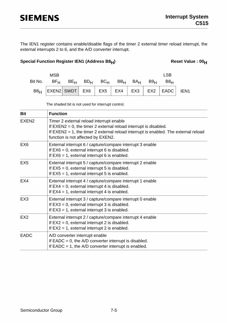
Interrupt SystemC515
The IEN1 register contains enable/disable flags of the timer 2 external timer reload interrupt, theexternal interrupts 2 to 6, and the A/D converter interrupt.
Special Function Register IEN1 (Address B8 H) Reset Value : 00 H
The shaded bit is not used for interrupt control.
Bit Function
EXEN2 Timer 2 external reload interrupt enableIf EXEN2 = 0, the timer 2 external reload interrupt is disabled. If EXEN2 = 1, the timer 2 external reload interrupt is enabled. The external reload function is not affected by EXEN2.
EX6 External interrupt 6 / capture/compare interrupt 3 enableIf EX6 = 0, external interrupt 6 is disabled.If EX6 = 1, external interrupt 6 is enabled.
EX5 External interrupt 5 / capture/compare interrupt 2 enableIf EX5 = 0, external interrupt 5 is disabled.If EX5 = 1, external interrupt 5 is enabled.
EX4 External interrupt 4 / capture/compare interrupt 1 enableIf EX4 = 0, external interrupt 4 is disabled.If EX4 = 1, external interrupt 4 is enabled.
EX3 External interrupt 3 / capture/compare interrupt 0 enableIf EX3 = 0, external interrupt 3 is disabled.If EX3 = 1, external interrupt 3 is enabled.
EX2 External interrupt 2 / capture/compare interrupt 4 enableIf EX2 = 0, external interrupt 2 is disabled.If EX2 = 1, external interrupt 2 is enabled.
EADC A/D converter interrupt enableIf EADC = 0, the A/D converter interrupt is disabled.If EADC = 1, the A/D converter interrupt is enabled.
EXEN2 SWDT EX6 EX5B8H IEN1
Bit No. BFH
MSB LSB
EX4 EX3 EX2 EADC
BEH BDH BCH BBH BAH B9H B8H
Semiconductor Group 7-5

Interrupt SystemC515
7.1.2 Interrupt Request / Control Flags
Special Function Register TCON (Address 88 H) Reset Value : 00 H
The shaded bits are not used for interrupt control.
The external interrupts 0 and 1 (INT0 and INT1) can each be either level-activated or negativetransition-activated, depending on bits IT0 and IT1 in register TCON. The flags that actuallygenerate these interrupts are bits IE0 and lE1 in TCON. When an external interrupt is generated, theflag that generated this interrupt is cleared by the hardware when the service routine is vectored too,but only if the interrupt was transition-activated. lf the interrupt was level-activated, then therequesting external source directly controls the request flag, rather than the on-chip hardware.
The timer 0 and timer 1 interrupts are generated by TF0 and TF1 in register TCON, which are setby a rollover in their respective timer/counter registers. When a timer interrupt is generated, the flagthat generated it is cleared by the on-chip hardware when the service routine is vectored too.
Bit Function
TF1 Timer 1 overflow flagSet by hardware on timer/counter 1 overflow. Cleared by hardware when processor vectors to interrupt routine.
TF0 Timer 0 overflow flagSet by hardware on timer/counter 0 overflow. Cleared by hardware when processor vectors to interrupt routine.
IE1 External interrupt 1 request flagSet by hardware when external interrupt 1 edge is detected. Cleared by hardware when processor vectors to interrupt routine.
IT1 External interrupt 1 level/edge trigger control flagIf IT1 = 0, low level triggered external interrupt 1 is selected.If IT1 = 1, falling edge triggered external interrupt 1 is selected.
IE0 External interrupt 0 request flagSet by hardware when external interrupt 0 edge is detected. Cleared by hardware when processor vectors to interrupt routine.
IT0 External interrupt 0 level/edge trigger control flagIf IT0 = 0, low level triggered external interrupt 0 is selected.If IT0 = 1, falling edge triggered external interrupt 0 is selected.
TF1 TR1 TF0 TR088H TCON
Bit No. 8FH
MSB LSB
IE1 IT1 IE0 IT0
8EH 8DH 8CH 8BH 8AH 89H 88H
Semiconductor Group 7-6

Interrupt SystemC515
Special Function Register T2CON (Address C8 H) Reset Value : 00 H
The shaded bits are not used for interrupt control.
The external interrupt 2 (INT2) can be either positive or negative transition-activated depending onbit I2FR in register T2CON. The flag that actually generates this interrupt is bit IEX2 in registerIRCON. lf an interrupt 2 is generated, flag IEX2 is cleared by hardware when the service routine isvectored to.
The external interrupt 3 (INT3) can be either positive or negative transition-activated, dependingon bit I3FR in register T2CON. The flag that actually generates this interrupt is bit IEX3 in registerIRCON. In addition, this flag will be set if a compare event occurs at pin P1.0/INT3/CC0, regardlessof the compare mode established and the transition at the respective pin. The flag IEX3 is clearedby hardware when the service routine is vectored to.
Bit Function
I3FR External interrupt 3 rising/falling edge control flagIf I3FR = 0, the external interrupt 3 is activated by a falling edge at P1.0/INT3/CC0.If I3FR = 1, the external interrupt 3 is activated by a rising edge at P1.0/INT3/CC0.
I2FR External interrupt 2 rising/falling edge control flagIf I2FR = 0, the external interrupt 2 is activated by a falling edge at P1.4/INT2.If I2FR = 1, the external interrupt 2 is activated by a rising edge at P1.4/INT2.
T2PS I3FR I2FR T2R1C8H T2CON
Bit No. CFH
MSB LSB
T2R0 T2CM T2I1 T2I0
CEH CDH CCH CBH CAH C9H C8H
Semiconductor Group 7-7

Interrupt SystemC515
Special Function Register IRCON (Address C0 H) Reset Value : 00 H
Bit Function
EXF2 Timer 2 external reload flagEXF2 is set when a reload is caused by a falling edge on pin T2EX while EXEN2 = 1. If ET2 in IEN0 is set (timer 2 interrupt enabled), EXF2 = 1 will cause an interrupt. EXF2 can be used as an additional external interrupt when the reload function is not used. EXF2 must be cleared by software.
TF2 Timer 2 overflow flagSet by a timer 2 overflow and must be cleared by software. If the timer 2 interrupt is enabled, TF2 = 1 will cause an interrupt.
IEX6 External interrupt 6 edge flagSet by hardware when external interrupt edge was detected or when a compare event occurred at pin P1.3/INT6/CC3. Cleared by hardware when processor vectors to interrupt routine.
IEX5 External interrupt 5 edge flagSet by hardware when external interrupt edge was detected or when a compare event occurred at pin P1.2/INT5/CC2. Cleared by hardware when processor vectors to interrupt routine.
IEX4 External interrupt 4 edge flagSet by hardware when external interrupt edge was detected or when a compare event occurred at pin P1.1/INT4/CC1. Cleared by hardware when processor vectors to interrupt routine.
IEX3 External interrupt 3 edge flagSet by hardware when external interrupt edge was detected or when a compare event occurred at pin P1.0/INT3/CC0. Cleared by hardware when processor vectors to interrupt routine.
IEX2 External interrupt 2 edge flagSet by hardware when external interrupt edge was detected at pin P1.4/INT2. Cleared by hardware when processor vectors to interrupt routine.
IADC A/D converter interrupt request flagSet by hardware at the end of an A/D conversion. Must be cleared by software.
EXF2 TF2 IEX6 IEX5C0H IRCON
Bit No. C7H
MSB LSB
IEX4 IEX3 IEX2 IADC
C6H C5H C4H C3H C2H C1H C0H
Semiconductor Group 7-8

Interrupt SystemC515
The timer 2 interrupt is generated by the logical OR of bit TF2 in register T2CON and bit EXF2 inregister IRCON. Neither of these flags is cleared by hardware when the service routine is vectoredto. In fact, the service routine may have to determine whether it was TF2 or EXF2 that generated theinterrupt, and the bit will have to be cleared by software.
The A/D converter interrupt is generated by IADC bit in register IRCON. If an interrupt isgenerated, in any case the converted result in ADDAT is valid on the first instruction of the interruptservice routine. lf continuous conversion is established, IADC is set once during each conversion.lf an A/D converter interrupt is generated, flag IADC will have to be cleared by software.
The external interrupts 4 to 6 (INT4, INT5, INT6) are positive transition-activated. The flags thatactually generate these interrupts are bits IEX4, IEX5, and IEX6 in register IRCON. In addition,these flags will be set if a compare event occurs at the corresponding output pin P1.1/ INT4/CC1,P1.2/INT5/CC2, and P1.3/INT6/CC3, regardless of the compare mode established and thetransition at the respective pin. When an interrupt is generated, the flag that generated it is clearedby the on-chip hardware when the service routine is vectored too.
All of these interrupt request bits that generate interrupts can be set or cleared by software, with thesame result as if they had been set or cleared by hardware. That is, interrupts can be generated orpending interrupts can be cancelled by software. The only exceptions are the request flags IE0 andlE1. lf the external interrupts 0 and 1 are programmed to be level-activated, IE0 and lE1 arecontrolled by the external source via pin INT0 and INT1, respectively. Thus, writing a one to thesebits will not set the request flag IE0 and/or lE1. In this mode, interrupts 0 and 1 can only begenerated by software and by writing a 0 to the corresponding pins INT0 (P3.2) and INT1 (P3.3),provided that this will not affect any peripheral circuit connected to the pins.
Semiconductor Group 7-9

Interrupt SystemC515
Special Function Register SCON (Address. 98 H) Reset Value : 00 H
The shaded bits are not used for interrupt control.
The serial port interrupt is generated by a logical OR of flag RI and TI in SFR SCON. Neither ofthese flags is cleared by hardware when the service routine is vectored too. In fact, the serviceroutine will normally have to determine whether it was the receive interrupt flag or the transmissioninterrupt flag that generated the interrupt, and the bit will have to be cleared by software.
Bit Function
TI Serial interface transmitter interrupt flagSet by hardware at the end of a serial data transmission. Must be cleared by software.
RI Serial interface receiver interrupt flagSet by hardware if a serial data byte has been received. Must be cleared by software.
SM0 SM1 SM2 REN98H SCON
Bit No. 9FH
MSB LSB
TB8 RB8 TI RI
9EH 9DH 9CH 9BH 9AH 99H 98H
Semiconductor Group 7-10

Interrupt SystemC515
7.1.3 Interrupt Priority Registers
The lower six bits of these two registers are used to define the interrupt priority level of the interruptgroups as they are defined in table 7-1 in the next section.
Special Function Register IP0 (Address A9 H) Reset Value : X0000000 BSpecial Function Register IP1 (Address B9 H) Reset Value : XX000000 B
The shaded bits are not used for interrupt control.
Bit Function
IP1.xIP0.x
Interrupt group priority level bits (x=1-6, see table 7-1 )
– WDTS IP0.5 IP0.4A9H IP0IP0.3 IP0.2 IP0.1 IP0.0
Bit No. 7 6 5 4 3 2 1 0MSB LSB
– – IP1.5 IP1.4B9H IP1IP1.3 IP1.2 IP1.1 IP1.0
Bit No. 7 6 5 4 3 2 1 0
IP1.x IP0.x Function
0 0 Interrupt group x is set to priority level 0 (lowest)
0 1 Interrupt group x is set to priority level 1
1 0 Interrupt group x is set to priority level 2
1 1 Interrupt group x is set to priority level 3 (highest)
Semiconductor Group 7-11

Interrupt SystemC515
7.2 Interrupt Priority Level Structure
The following table shows the interrupt grouping of the C515 interrupt sources.
Each pair of interrupt sources can be programmed individually to one of four priority levels by settingor clearing one bit in the special function register IP0 and one in IP1. A low-priority interrupt can beinterrupted by a high-priority interrupt, but not by another interrupt of the same or a lower priority. Aninterrupt of the highest priority level cannot be interrupted by another interrupt source.
lf two or more requests of different priority leveis are received simultaneously, the request of thehighest priority is serviced first. lf requests of the same priority level are received simultaneously, aninternal polling sequence determines which request is to be serviced first. Thus, within each prioritylevel there is a second priority structure determined by the polling sequence, as follows.
– Within one interrupt group the „left“ interrupt is serviced first– The interrupt groups are serviced from top to bottom of the table.
Table 7-1 Interrupt Source Structure
InterruptGroup
Associated Interrupts Priority
1 External interrupt 0 A/D converter interrupt High
Low
2 Timer 0 overflow External interrupt 2
3 External interrupt 1 External interrupt 3
4 Timer 1 overflow External interrupt 4
5 Serial channel interrupt External interrupt 5
6 Timer 2 interrupt External interrupt 6
High Priority Low Priority
Semiconductor Group 7-12

Interrupt SystemC515
7.3 How Interrupts are Handled
The interrupt flags are sampled at S5P2 in each machine cycle. The sampled flags are polled duringthe following machine cycle. If one of the flags was in a set condition at S5P2 of the preceedingcycle, the polling cycle will find it and the interrupt system will generate a LCALL to the appropriateservice routine, provided this hardware-generated LCALL is not blocked by any of the followingconditions:
1. An interrupt of equal or higher priority is already in progress.2. The current (polling) cycle is not in the final cycle of the instruction in progress.3. The instruction in progress is RETI or any write access to registers IEN0 and IEN1 or IP0/IP1.
Any of these three conditions will block the generation of the LCALL to the interrupt service routine.Condition 2 ensures that the instruction in progress is completed before vectoring to any serviceroutine. Condition 3 ensures that if the instruction in progress is RETI or any write access toregisters IEN0/IEN1 or IP0/IP1, then at least one more instruction will be executed before anyinterrupt is vectored too; this delay guarantees that changes of the interrupt status can be observedby the CPU.
The polling cycle is repeated with each machine cycle, and the values polled are the values thatwere present at S5P2 of the previous machine cycle. Note that if any interrupt flag is active but notbeing responded to for one of the conditions already mentioned, or if the flag is no longer activewhen the blocking condition is removed, the denied interrupt will not be serviced. In other words, thefact that the interrupt flag was once active but not serviced is not remembered. Every polling cycleinterrogates only the pending interrupt requests.
The polling cycle/LCALL sequence is illustrated in figure 7-3 .
Figure 7-3 Interrupt Response Timing Diagram
MCT01859
S5P2
Interruptis latched
Interruptsare polled Vector Address
Long Call to InterruptRoutineInterrupt
C2C1 C3 C4 C5
Semiconductor Group 7-13

Interrupt SystemC515
Note that if an interrupt of a higher priority level goes active prior to S5P2 in the machine cyclelabeled C3 in figure 7-3 then, in accordance with the above rules, it will be vectored to during C5and C6 without any instruction for the lower priority routine to be executed.
Thus, the processor acknowledges an interrupt request by executing a hardware-generated LCALLto the appropriate servicing routine. In some cases it also clears the flag that generated theinterrupt, while in other cases it does not; then this has to be done by the user's software. Thehardware clears the external interrupt flags IE0 and IE1 only if they were transition-activated. Thehardware-generated LCALL pushes the contents of the program counter onto the stack (but it doesnot save the PSW) and reloads the program counter with an address that depends on the source ofthe interrupt being vectored too, as shown in the following table 7-2 .
Execution proceeds from that location until the RETI instruction is encountered. The RETIinstruction informs the processor that the interrupt routine is no longer in progress, then pops thetwo top bytes from the stack and reloads the program counter. Execution of the interrupted programcontinues from the point where it was stopped. Note that the RETI instruction is very importantbecause it informs the processor that the program left the current interrupt priority level. A simpleRET instruction would also have returned execution to the interrupted program, but it would haveleft the interrupt control system thinking an interrupt was still in progress. In this case no interrupt ofthe same or lower priority level would be acknowledged.
Table 7-2 Interrupt Source and Vectors
Interrupt Source Interrupt Vector Address Interrupt Request Flags
External Interrupt 0 0003H IE0
Timer 0 Overflow 000BH TF0
External Interrupt 1 0013H IE1
Timer 1 Overflow 001BH TF1
Serial Channel 0023H RI / TI
Timer 2 Overflow / Ext. Reload 002BH TF2 / EXF2
A/D Converter 0043H IADC
External Interrupt 2 004BH IEX2
External Interrupt 3 0053H IEX3
External Interrupt 4 005BH IEX4
External Interrupt 5 0063H IEX5
External Interrupt 6 006BH IEX6
Semiconductor Group 7-14
Interrupt SystemC515
7.4 External Interrupts
The external interrupts 0 and 1 can be programmed to be level-activated or negative-transitionactivated by setting or clearing bit IT0, respectively in register TCON. If ITx = 0 (x = 0 or 1), externalinterrupt x is triggered by a detected low level at the INTx pin. If ITx = 1, external interrupt x isnegative edge-triggered. In this mode, if successive samples of the INTx pin show a high in onecycle and a low in the next cycle, interrupt request flag IEx in TCON is set. Flag bit IEx=1 thenrequests the interrupt.
If the external interrupt 0 or 1 is level-activated, the external source has to hold the request activeuntil the requested interrupt is actually generated. Then it has to deactivate the request before theinterrupt service routine is completed, or else another interrupt will be generated.
The external interrupts 2 and 3 can be programmed to be negative or positive transition-activatedby setting or clearing bit I2FR or I3FR in register T2CON. lf IxFR = 0 (x = 2 or 3), the externalinterrupt x is negative transition-activated. lf IxFR = 1, the external interrupt is triggered by a positivetransition.
The external interrupts 4, 5, and 6 are activated only by a positive transition. The external timer 2reload trigger interrupt request flag EXF2 will be activated by a negative transition at pin Pl.5/T2EXbut only if bit EXEN2 is set.
Since the external interrupt pins (INT2 to INT6) are sampled once in each machine cycle, an inputhigh or low should be held for at least 6 oscillator periods to ensure sampling. lf the external interruptis transition-activated, the external source has to hold the request pin low (high for INT2 and INT3,if it is programmed to be negative transition-active) for at least one cycle, and then hold it high (low)for at least one cycle to ensure that the transition is recognized so that the corresponding interruptrequest flag will be set (see figure 7-4 ). The external interrupt request flags will automatically becleared by the CPU when the service routine is called.
Semiconductor Group 7-15

Interrupt SystemC515
Figure 7-4 External Interrupt Detection
MCD01860
P3.x/INTx
e.g. P3.x/INTx
> 1 Machine Cycle
Low-Level Threshold
> 1 Machine Cycle > 1 Machine Cycle
Transition tobe detected
High-Level Threshold
Low-Level Threshold
b) Transition-Activated Interrupt
a) Level-Activated Interrupt
Semiconductor Group 7-16

Interrupt SystemC515
7.5 Interrupt Response Time
If an external interrupt is recognized, its corresponding request flag is set at S5P2 in every machinecycle. The value is not polled by the circuitry until the next machine cycle. If the request is active andconditions are right for it to be acknowledged, a hardware subroutine call to the requested serviceroutine will be next instruction to be executed. The call itself takes two cycles. Thus a minimum ofthree complete machine cycles will elapse between activation and external interrupt request and thebeginning of execution of the first instruction of the service routine.
A longer response time would be obtained if the request was blocked by one of the three previouslylisted conditions. If an interrupt of equal or higer priority is already in progress, the additional waittime obviously depends on the nature of the other interrupt's service routine. If the instruction inprogress is not in its final cycle, the additional wait time cannot be more than 3 cycles since thelongest instructions (MUL and DIV) are only 4 cycles long; and, if the instruction in progress is RETIor a write access to registers IEN0, IEN1 or IP0, IP1 the additional wait time cannot be more than5 cycles (a maximum of one more cycle to complete the instruction in progress, plus 4 cycles tocomplete the next instruction, if the instruction is MUL or DIV).
Thus a single interrupt system, the response time is always more than 3 cycles and less than9 cycles.
Semiconductor Group 7-17

Fail Safe MechanismsC515
8 Fail Safe Mechanisms
8.1 Watchdog Timer
8.1.1 General Operation
As a means of graceful recovery from software or hardware upset a watchdog timer is provided inthe C515. lf the software fails to clear the watchdog timer at least every 65532 ms (at 12 MHz clockrate), an internal hardware reset will be initiated. The software can be designed such that thewatchdog times out if the program does not progress properly. The watchdog will also time out if thesoftware error was due to hardware-related problems. This prevents the controller frommalfunctioning for longer than 65 ms if a 12-MHz oscillator is used.
The watchdog timer is a 16-bit counter which is incremented once every machine cycle. After anexternal reset the watchdog timer is disabled and cleared to 0000H.
8.1.2 Starting the Watchdog Timer
There are two ways to start the watchdog timer depending on the level applied to pin PE/SWD. Thispin serves two functions, because it is also used for blocking the power saving modes. (see alsochapter 9 ).
8.1.2.1 The First Possibility of Starting the Watchdog Timer
The automatic start of the watchdog timer directly during an external HW reset is achieved bystrapping pin PE/SWD to VCC. In this case the power saving modes (power down mode, idle modeand slow down mode) are also disabled and cannot be started by software. If pin PE/SWD is leftunconnected, a weak pull-up transistor ensures the automatic start of the watchdog timer.
The self-start of the watchdog timer by a pin option has been implemented to provide high systemsecurity in electrically very noisy environments.
Note: The automatic start of the watchdog timer is only performed if PE/SWD (power-saveenable/start watchdog timer) is held at high level while RESET is active. A positive transitionat PE/SWD pin during normal program execution will not start the watchdog timer.
8.1.2.2 The Second Possibility of Starting the Watchdog Timer
The watchdog timer can also be started by software. Setting of bit SWDT in SFR IEN1 starts thewatchdog timer. After having been started, the bit WDTS in SFR IP0 is set. Note that the watchdogtimer cannot be stopped by software.
See chapter 9 for entering the power saving modes by software.
Semiconductor Group 8-1

Fail Safe MechanismsC515
8.1.3 Refreshing the Watchdog Timer
Once started, the watchdog timer can only be cleared to 0000H by first setting bit WDT and with thenext instruction setting bit SWDT. Bit WDT will automatically be cleared during the second machinecycle after having been set. For this reason, setting SWDT bit has to be a one cycle instruction (e.g.SETB SWDT). This double instruction clearing of the watchdog timer was implemented to minimizethe chance of unintentionally clearing the watchdog. To prevent the watchdog from overflowing, itmust be cleared periodically.
Setting only bit SWDT does not reload the watchdog timer automatically to 0000H. A watchdogtimer reset operation occurs only by using the double instruction refresh sequence SETB WDT /SETB SWDT.
8.1.4 Watchdog Reset and Watchdog Status Flag
lf the software fails to clear the watchdog in time, an internally generated watchdog reset is enteredat the counter state FFFCH and lasts four instruction cycles. This internal reset differs from anexternal reset only to the extent that the watchdog timer is not disabled. Bit WDTS allows thesoftware to examine from which source the reset was initiated. lf it is set, the reset was caused bya watchdog timer overflow.
Figure 8-1 shows a block diagram of the watchdog timer.
Figure 8-1 Block Diagram of the Watchdog Timer
MCB03210
Control Logic
WDT Reset if WDT count is between
IEN1
IEN0
)( B8H
HA8( )
16-Bit Watchdog Timer
IP0 ( A9H)
WDT
SWDT -
-
-
-
-
-
-
-
-
-
-
--
-
External HW Reset
- ------WDTS
OSCf÷ 12
Reset
FFFCH HFFFF-
PE/SWD
Semiconductor Group 8-2

Fail Safe MechanismsC515
8.1.5 WDT Control and Status Flags
The watchdog timer is controlled by two control flags (located in SFR IEN0 and IEN1) and onestatus flags (located in SFR IP0).
Special Function Register IEN0 (Address A8 H) Reset Value : 00 HSpecial Function Register IEN1 (Address B8 H) Reset Value : 00 HSpecial Function Register IP0 (Address A9 H) Reset Value : X0000000 B
The shaded bits are not used for fail save control.
Bit Function
WDT Watchdog timer refresh flag.Set to initiate a refresh of the watchdog timer. Must be set directly before SWDT is set to prevent an unintentional refresh of the watchdog timer. WDT is reset by hardware two processor cycles after it has been set.
SWDT Watchdog timer start/refresh flag.Set to activate the watchdog timer. When directly set after setting WDT, a watchdog timer refresh/reset is performed. Bit SDWT is reset by hardware two processor cycles after it has been set.
WDTS Watchdog timer status flag.Set by hardware when a watchdog Timer reset occured. Can be cleared and set by software.
EAL WDT ET2 ESA8H IEN0
AFH
MSB LSB
ET1 EX1 ET0 EX0
AEH ADH ACH ABH AAH A9H A8H
EXEN2 SWDT EX6 EX5B8H IEN1
BFH
EX4 EX3 EX2 EADC
BEH BDH BCH BBH BAH B9H B8H
– WDTS IP0.5 IP0.4A9H IP0IP0.3 IP0.2 IP0.1 IP0.0
Bit No. 7 6 5 4 3 2 1 0
Semiconductor Group 8-3

Power Saving ModesC515
9 Power Saving Modes
The C515 provides two basic power saving modes, the idle mode and the power down mode.Additionally, a slow down mode is available. This power saving mode reduces the internal clock ratein normal operating mode and it can be also used for further power reduction in idle mode. All thepower saving modes are initiated by software.
9.1 Hardware Enable for the Use of the Power Saving Modes
To provide power saving modes together with effective protection against unintentional entering ofthese modes, the C515 has an extra pin disabling the use of the power saving modes. As this pinwill most likely be used only in critical applications it is combined with an automatic start of thewatchdog timer (see the description in chapter 8 “Fail Save Mechanisms”). This pin is called PE/SWD (power saving enable/start watchdog timer) and its function is as follows:
PE/SWD = 1 (logic high level)
– Use of the power saving modes is not possible. The instruction sequences used for enteringthese modes will not affect the normal operation of the device.
– lf and only if PE/SWD is held at high level during reset, the watchdog timer is startedimmediately after reset is released.
PE/SWD = 0 (logic low level)
– All power saving modes can be activated as described in the following sections– The watchdog timer has to be started by software if system protection is desired.
When left unconnected, the pin PE/SWD is pulled to high level by a weak internal pullup. This isdone to provide system protection by default.
The logic level applied to pin PE/SWD can be changed during program execution in order to allowor block the use of the power saving modes without any effect on the on-chip watchdog circuitry;(the watchdog timer is started only if PE/SWD is on high level up to the moment when reset isreleased; a change at PE/SWD during program execution has no effect on the watchdog timer; thisonly enables or disables the use of the power saving modes.). A change of the pin’s level is detectedin state 3, phase 1. A Schmitt trigger is used at the input to reduce susceptibility to noise.
In addition to the hardware enable/disable of the power saving modes, a double-instructionsequence which is described in the corresponding sections is necessary to enter power down andidle mode. The combination of all these safety precautions provide a maximum of systemprotection.
Application Example for Switching Pin PE /SWD
For most applications in noisy environments, components external to the chip are used to givewarning of a power failure or a turn off of the power supply. These circuits could be used to controlthe PE/SWD pin. The possible steps to go into power down mode could then be as follows:
– A power-fail signal forces the controller to go into a high priority interrupt routine. This interruptroutine saves the actual program status. At the same time pin PE/SWD is pulled low by thepower-fail signal.
– Finally the controller enters power down mode by executing the relevant double-instructionsequence.
Semiconductor Group 9-1

Power Saving ModesC515
9.2 Power Saving Mode Control Register
The functions of the power saving modes are controlled by bits which are located in the specialfunction register PCON. The bits PDE, PDS and IDLE, IDLS located in SFR PCON select the powerdown mode or the idle mode, respectively. If the power down mode and the idle mode are set at thesame time, power down takes precedence. Furthermore, register PCON contains two generalpurpose flags. For example, the flag bits GF0 and GF1 can be used to give an indication if aninterrupt occurred during normal operation or during an idle. For this, an instruction that activatesidle can also set one or both flag bits. When idle is terminated by an interrupt, the interrupt serviceroutine can examine the flag bits.
Special Function Register PCON (Address 87 H) Reset Value : 00 H
Note: The PDS bit, which controls the software power down mode is forced to logic low wheneverthe external PE/SWD pin is held at logic high level. Changing the logic level of the PE/SWDpin from high to low will irregularly terminate the software power down mode and is notpermitted.
Symbol Function
PDS Power down start bitThe instruction that sets the PDS flag bit is the last instruction before entering the power down mode
IDLS Idle start bitThe instruction that sets the IDLS flag bit is the last instruction before entering the idle mode.
SD Slow down mode bitWhen set, the slow down mode is enabled. This function is available in the C515-LM/1RM versions only.
GF1 General purpose flag
GF0 General purpose flag
PDE Power down enable bitWhen set, starting of the power down is enabled
IDLE Idle mode enable bitWhen set, starting of the idle mode is enabled
MSB LSB
87H PCONSMOD PDS IDLS SD GF1 GF0 PDE IDLE
7 6 5 4 3 2 1 0Bit No.
The function of the shaded bit is not described in this section.
Semiconductor Group 9-2

Power Saving ModesC515
9.3 Idle Mode
In the idle mode the oscillator of the C515 continues to run, but the CPU is gated off from the clocksignal. However, the interrupt system, the serial port, the A/D converter, and all timers with theexception of the watchdog timer are further provided with the clock. The CPU status is preserved inits entirety: the stack pointer, program counter, program status word, accumulator, and all otherregisters maintain their data during idle mode.
The reduction of power consumption, which can be achieved by this feature depends on the numberof peripherals running. If all timers are stopped and the A/D converter, and the serial interfaces arenot running, the maximum power reduction can be achieved. This state is also the test condition forthe idle mode ICC.
Thus, the user has to take care which peripheral should continue to run and which has to be stoppedduring idle mode. Also the state of all port pins – either the pins controlled by their latches orcontrolled by their secondary functions – depends on the status of the controller when entering idlemode.
Normally, the port pins hold the logical state they had at the time when the idle mode was activated.If some pins are programmed to serve as alternate functions they still continue to output during idlemode if the assigned function is on. This especially applies to the serial interface in case it cannotfinish reception or transmission during normal operation. The control signals ALE and PSEN areheld at logic high levels.
As in normal operation mode, the ports can be used as inputs during idle mode. Thus a capture orreload operation can be triggered, the timers can be used to count external events, and externalinterrupts will be detected.
The idle mode is a useful feature which makes it possible to "freeze" the processor's status - eitherfor a predefined time, or until an external event reverts the controller to normal operation, asdiscussed below. The watchdog timer is the only peripheral which is automatically stopped duringidle mode.
Semiconductor Group 9-3
Power Saving ModesC515
The idle mode is entered by two consecutive instructions. The first instruction sets the flag bit IDLE(PCON.0) and must not set bit IDLS (PCON.5), the following instruction sets the start bit IDLS(PCON.5) and must not set bit IDLE (PCON.0). The hardware ensures that a concurrent setting ofboth bits, IDLE and IDLS, does not initiate the idle mode. Bits IDLE and IDLS will automatically becleared after being set. If one of these register bits is read the value that appears is 0. This doubleinstruction is implemented to minimize the chance of an unintentional entering of the idle modewhich would leave the watchdog timer's task of system protection without effect.
Note:
PCON is not a bit-addressable register, so the above mentioned sequence for entering the idlemode is obtained by byte-handling instructions, as shown in the following example:
ORL PCON,#00000001B ;Set bit IDLE, bit IDLS must not be setORL PCON,#00100000B ;Set bit IDLS, bit IDLE must not be set
The instruction that sets bit IDLS is the last instruction executed before going into idle mode.
There are two ways to terminate the idle mode:
– The idle mode can be terminated by activating any enabled interrupt. The CPU operation isresumed, the interrupt will be serviced and the next intsruction to be executed after the RETIinstruction will be the one following the instruction that had set the bit IDLS.
– The other way to terminate the idle mode, is a hardware reset. Since the oscillator is stillrunning, the hardware reset must be held active only for two machine cycles for a completereset.
Semiconductor Group 9-4

Power Saving ModesC515
9.4 Slow Down Mode Operation (C515-LM/1RM only)
In some applications, where power consumption and dissipation are critical, the controller might runfor a certain time at reduced speed (e.g. if the controller is waiting for an input signal). Since inCMOS devices there is an almost linear dependence of the operating frequency and the powersupply current, a reduction of the operating frequency results in reduced power consumption.
In the slow down mode all signal frequencies that are derived from the oscillator clock are dividedby 8.
The slow down mode is activated by setting the bit SD in SFR PCON. If the slow down mode isenabled, the clock signals for the CPU and the peripheral units are reduced to 1/8 of the nominalsystem clock rate. The controller actually enters the slow down mode after a short synchronizationperiod (max. two machine cycles). The slow down mode is terminated by clearing bit SD.
The slow down mode can be combined with the idle mode by performing the following doubleinstruction sequence:
ORL PCON,#00000001B ; preparing idle mode: set bit IDLE (IDLS not set)ORL PCON,#00110000B ; entering idle mode combined with the slow down mode:
; (IDLS and SD set)
There are two ways to terminate the combined Idle and Slow Down Mode :
– The idle mode can be terminated by activation of any enabled interrupt. The CPU operationis resumed, the interrupt will be serviced and the next instruction to be executed after the RETIinstruction will be the one following the instruction that had set the bits IDLS and SD.Nevertheless the slow down mode keeps enabled and if required has to be terminated byclearing the bit SD in the corresponding interrupt service routine or at any point in the programwhere the user no longer requires the slow-down mode power saving.
– The other possibility of terminating the combined idle and slow down mode is a hardwarereset. Since the oscillator is still running, the hardware reset has to be held active for only twomachine cycles for a complete reset.
The slow down feature is not available for C515-LN/1RN versions.
Semiconductor Group 9-5

Power Saving ModesC515
9.5 Power Down Mode
In the power down mode, the RC osciillator and the on-chip oscillator which operates with the XTALpins is stopped. Therefore, all functions of the microcontroller are stopped and only the contents ofthe on-chip RAM and the SFR's are maintained. The port pins, which are controlled by their portlatches, output the values that are held by their SFR's. The port pins which serve the alternateoutput functions show the values they had at the end of the last cycle of the instruction whichinitiated the power down mode. ALE and PSEN held at logic low level (see table 9-1 ).
In the power down mode of operation, VCC can be reduced to minimize power consumption. It mustbe ensured, however, that is VCC not reduced before the power down mode is invoked, and that VCC
is restored to its normal operating level before the power down mode is terminated.
The power down mode can be left only by a hardware reset. Leaving the power down mode puts themicrocontroller with its SFRs into the reset state, and it should not be done before VCC is restoredto its nominal operating level.
9.5.1 Invoking Power Down Mode
The power down mode is entered by two consecutive instructions. The first instruction has to set theflag bit PDE (PCON.1) and must not set bit PDS (PCON.6), the following instruction has to set thestart bit PDS (PCON.6) and must not set bit PDE (PCON.1). The hardware ensures that aconcurrent setting of both bits, PDE and PDS, does not initiate the power down mode. Bits PDE andPDS will automatically be cleared after having been set and the value shown by reading one ofthese bits is always 0. This double instruction is implemented to minimize the chance ofunintentionally entering the power down mode which could possibly ”freeze” the chip's activity in anundesired status.
PCON is not a bit-addressable register, so the above mentioned sequence for entering the powerdown mode is obtained by byte-handling instructions, as shown in the following example:
ORL PCON,#00000010B ;set bit PDE, bit PDS must not be setORL PCON,#01000000B ;set bit PDS, bit PDE must not be set, enter power down
The instruction that sets bit PDS is the last instruction executed before going into power downmode. When the double instruction sequence shown above is used, the power down mode can onlybe left by a reset operation.
Note : Before entering the power down mode, an A/D conversion in progress must be stopped.
9.5.2 Exit from Power Down Mode
If power down mode is exit via a hardware reset, the microcontroller with its SFRs is put into thehardware reset state and the content of RAM is not changed. The reset signal that terminates thepower down mode also restarts the RC oscillator and the on-chip oscillatror. The reset operationshould not be activated before VCC is restored to its normal operating level and must be held activelong enough to allow the oscillator to restart and stabilize (similar to power-on reset).
Semiconductor Group 9-6

Power Saving ModesC515
9.6 State of Pins in the Power Saving Modes
In the idle mode and in the power down mode the port pins of the C515 have a well defined statuswhich is listed in the following table 9-1 . This state of some pins also depends on the location of thecode memory (internal or external).
Table 9-1 Status of External Pins During Idle and Software Power Down Mode
Outputs Last Instruction Executed from Internal Code Memory
Last Instruction Executed from External Code Memory
Idle Power Down Idle Power Down
ALE High Low High Low
PSEN High Low High Low
PORT 0 Data Data Float Float
PORT 2 Data Data Address Data
PORT 1, 3, 4 Data /alternate outputs
Data /last output
Data /alternate outputs
Data /last output
Semiconductor Group 9-7

Device SpecificationsC515
10 Device Specifications
10.1 Absolute Maximum Ratings
Ambient temperature under bias (TA) .............................................................. 0 ̊C to + 110 ˚CStorage temperature (TST) ...............................................................................– 65 ˚C to + 150 ˚CVoltage on VCC pins with respect to ground (VSS) ............................................– 0.5 V to 6.5 VVoltage on any pin with respect to ground (VSS) ..............................................– 0.5 V to VCC + 0.5 VInput current on any pin during overload condition..........................................– 10 mA to + 10 mAAbsolute sum of all input currents during overload condition ..........................| 100 mA |Power dissipation.............................................................................................TBD
Note: Stresses above those listed under “Absolute Maximum Ratings” may cause permanentdamage of the device. This is a stress rating only and functional operation of the device atthese or any other conditions above those indicated in the operational sections of thisspecification is not implied. Exposure to absolute maximum rating conditions for longerperiods may affect device reliability. During overload conditions (VIN > VCC or VIN < VSS) theVoltage on VCC pins with respect to ground (VSS) must not exceed the values defined by theabsolute maximum ratings.
Semiconductor Group 10-1

Device SpecificationsC515
10.2 DC Characteristics
VCC = 5 V + 10%, – 15%; VSS = 0 V TA = 0 to 70 °C for the SAB-C515TA = – 40 to 85 °C for the SAF-C515TA = – 40 to 110 °C for the SAH-C515
Notes see next page
Parameter Symbol Limit Values Unit Test Condition
min. max.
Input low voltages all except EAEA pin
VIL
VIL1
– 0.5– 0.5
0.2 VCC - 0.10.2 VCC - 0.3
VV
––
Input high voltagesall except XTAL2 and RESETXTAL2 pinRESET pin
VIH
VIH1
VIH2
0.2 VCC + 0.90.7 VCC
0.6 VCC
VCC + 0.5VCC + 0.5VCC + 0.5
VVV
–––
Output low voltagesPorts 1, 2, 3, 4, 5Port 0, ALE, PSEN
VOL
VOL1
––
0.450.45
VV
IOL = 1.6 mA 1)
IOL = 3.2 mA 1)
Output high voltages Ports 1, 2, 3, 4, 5
Port 0 an 2 in external bus mode, ALE, PSEN
VOH
VOH2
2.40.9 VCC
2.40.9 VCC
––––
VVVV
IOH = – 80 mAIOH = – 10 mA)
IOH = – 800 mA 2)
IOH = – 80 mA 2)
Logic 0 input current Ports 1, 2, 3, 4, 5 IIL – 10 – 70 mA VIN = 0.45 V
Logical 0-to-1 transition current Ports 1, 2, 3, 4, 5
ITL – 65 – 650 mA VIN = 2 V
Input leakage current Port 0, AIN0-7 (Port 6), EA ILI – ± 1 mA 0.45 < VIN < VCC
Input low currentto RESET for resetXTAL2PE
ILI2
ILI3
ILI4
–10––
– 100– 15– 20
mAmAmA
VIN = 0.45 VVIN = 0.45 VVIN = 0.45 V
Pin capacitance CIO – 10 pF fc = 1 MHz,TA = 25 °C
Overload current IOV – ± 5 mA 7) 8)
Semiconductor Group 10-2

Device SpecificationsC515
Power Supply Current
1) Capacitive loading on ports 0 and 2 may cause spurious noise pulses to be superimposed on the VOL of ALEand ports1, 3, 4, and 5. The noise is due to external bus capacitance discharging into the port 0 and port 2 pinswhen these pins make 1-to-0 transitions during bus operation. In the worst case (capacitive loading > 100 pF),the noise pulse on ALE line may exceed 0.8 V. In such cases it may be desirable to qualify ALE with a schmitt-trigger, or use an address latch with a schmitt-trigger strobe input.
2) Capacitive loading on ports 0 and 2 may cause the VOH on ALE and PSEN to momentarily fall below the0.9 VCC specification when the address lines are stabilizing.
3) IPD (power-down mode) is measured under following conditions:EA = Port 0 = Port 6 =VCC ; RESET = VCC; XTAL1 = N.C.; PE = XTAL2 = VSS ; VAGND = VSS ; VAREF = VCC ; allother pins are disconnected. The typical IPD current is measured at VCC = 5V.
4) ICC (active mode) is measured with: XTAL2 driven with tCLCH , tCHCL = 5 ns , VIL = VSS + 0.5 V, VIH = VCC – 0.5 V; XTAL1 = N.C.;EA = Port 0 = Port 6 = VCC ; RESET = VSS ; all other pins are disconnected.
5) ICC (idle mode) is measured with all output pins disconnected and with all peripherals disabled;XTAL2 driven with tCLCH , tCHCL = 5 ns, VIL = VSS + 0.5 V, VIH = VCC – 0.5 V; XTAL1 = N.C.;EA = Port 0 = Port 6 = VCC ; RESET = VCC ; all other pins are disconnected;
6) ICC (active mode with slow-down mode) is measured with : XTAL2 driven with tCLCH , tCHCL = 5 ns , VIL = VSS + 0.5 V, VIH = VCC – 0.5 V; XTAL1 = N.C.;EA = Port 0 = Port 6 = VCC ; RESET = VCC ; all other pins are disconnected; the microcontroller is put intoslow-down mode by software; all peripheral units are not activated.
7) Overload conditions occur if the standard operating conditions are exceeded, ie. the voltage on any pinexceeds the specified range (i.e. VOV > VCC + 0.5 V or VOV < VSS - 0.5 V). The supply voltage VCC and VSS mustremain within the specified limits. The absolute sum of input currents on all port pins may not exceed 50 mA.
8) Not 100% tested, guaranteed by design characterization
9) The typical ICC values are periodically measured at TA = +25 ˚C and VCC = 5 V but not 100% tested.
10)The maximum ICC values are measured under worst case conditions (TA = 0 ˚C or -40 ˚C and VCC = 5.5 V)
Parameter Symbol Limit Values Unit Test Condition
typ. 9) max. 10)
Active mode 12 MHz16 MHz24 MHz
ICC
ICC
ICC
11.013.719.1
14.818.225
mAmAmA
4)
Idle mode 12 MHz16 MHz24 MHz
ICC
ICC
ICC
5.86.99.1
8.19.612.8
mAmAmA
5)
Active mode with slow-down enabled
12 MHz16 MHz24 MHz
ICC
ICC
ICC
4.24.96.3
6.17.08.8
mAmAmA
6)
Power-down mode IPD 10 30 mA 3)
Semiconductor Group 10-3

Device SpecificationsC515
ICC Diagram
MCD03282
00
f OSC
CCI
4 8 12 16 20 24
5
10
15
20
25
30
MHz
mA
Active Mode
Idle Mode
Active Mode with Slow Down
= 0.68 x + 2.8f OSCCC typI:= 0.85 x + 4.6: CC maxI OSCf
= 0.39 x + 3.4= 0.28 x + 2.4
::
CC max
CC typ
II
OSC
OSC
ff
= 0.18 x + 2.0= 0.23 x + 3.3:
:
CC maxICC typI
OSCfOSCf
Active mode
Idle mode
Active mode with slow-down
is the oscillator frequency in MHz. values are given in mA.I CCOSCf
CC typII CC max
Active Mode
Idle Mode
Semiconductor Group 10-4

Device SpecificationsC515
10.3 A/D Converter Characteristics
VCC = 5 V + 10%, – 15%; VSS = 0 V TA = 0 to 70 °C for the SAB-C515TA = – 40 to 85 °C for the SAF-C515TA = – 40 to 110 °C for the SAH-C515
VCC – 0.25 V £ VAREF £ VCC + 0.1 V ; VSS – 0.1 V £ VAGND £ VSS + 0.2 V; VIntAREF - VIntAGND ³ 1 V;
Notes:
1) VAIN may exeed VAGND or VAREF up to the absolute maximum ratings. However, the conversion result inthese cases will be 00H or FFH, respectively.
2) During the sample time the input capacitance CAIN can be charged/discharged by the external source. Theinternal resistance of the analog source must allow the capacitance to reach their final voltage level within tS.After the end of the sample time tS, changes of the analog input voltage have no effect on the conversionresult.
3) This parameter includes the sample time tS and the conversion time tCO. The values for the conversion clocktADC is always 4 x tIN.
4) TUE is tested at VAREF = 5.0 V, VAGND = 0 V, VCC = 4.9 V. It is guaranteed by design characterization for allother voltages within the defined voltage range. If an overload condition occurs on maximum 2 not selected analog input pins and the absolute sum of inputoverload currents on all analog input pins does not exceed 10 mA, an additional conversion error of 1/2 LSBis permissible.
5) During the conversion the ADC’s capacitance must be repeatedly charged or discharged. The internalresistance of the reference source must allow the capacitance to reach their final voltage level within theindicated time. The maximum internal resistance results from the programmed conversion timing.
6) Not 100% tested, but guaranteed by design characterization.
Parameter Symbol Limit Values Unit Test Condition
min. max.
Analog input voltage VAIN VAGND -
0.2VAREF +0.2
V 1)
A/D converter input clock t IN – 2 x t CLCL ns
Sample time tS – 40 x tIN ns 2)
Conversion cycle time tADCC – 72 x tIN ns 3)
Total unadjusted error TUE – ± 1 LSB VIntAREF = VAREF = VCC
VIntAGND = VAGND = VSS 4)
Internal resistance of reference voltage source
RAREF – 4 x tIN /500 - 1
kW tIN in [ns] 5) 6)
Internal resistance of analog source
RASRC – tS / 500 - 1 kW tS in [ns] 2) 6)
ADC input capacitance CAIN – 45 pF 6)
Semiconductor Group 10-5

Device SpecificationsC515
10.4 AC Characteristics (16 MHz)
VCC = 5 V + 10%, – 15%; VSS = 0 V TA = 0 to 70 °C for the SAB-C515TA = – 40 to 85 °C for the SAF-C515TA = – 40 to 110 °C for the SAH-C515
(CL for port 0, ALE and PSEN outputs = 100 pF; CL for all other outputs = 80 pF)
Program Memory Characteristics
*) Interfacing the C515 to devices with float times up to 55 ns is permissible. This limited bus contention will notcause any damage to port 0 drivers.
CLKOUT Timing
Parameter Symbol Limit Values Unit
16 MHz Clock
Variable Clock1/tCLCL = 1 MHz to 16 MHz
min. max. min. max.
ALE pulse width tLHLL 85 – 2tCLCL – 40 – ns
Address setup to ALE tAVLL 33 – tCLCL – 30 – ns
Address hold after ALE tLLAX 28 – tCLCL – 35 – ns
ALE low to valid instruction in tLLIV – 150 – 4tCLCL – 100 ns
ALE to PSEN tLLPL 38 – tCLCL – 25 – ns
PSEN pulse width tPLPH 153 – 3tCLCL – 35 – ns
PSEN to valid instruction in tPLIV – 88 – 3tCLCL – 100 ns
Input instruction hold after PSEN tPXIX 0 – 0 – ns
Input instruction float after PSEN tPXIZ*) – 43 – tCLCL – 20 ns
Address valid after PSEN tPXAV*) 55 – tCLCL – 8 – ns
Address to valid instruction in tAVIV – 198 – 5tCLCL – 115 ns
Address float to PSEN tAZPL 0 – 0 – ns
Parameter Symbol Limit Values Unit
16 MHz Clock
Variable Clock1/tCLCL = 3.5 MHz to 16 MHz
min. max. min. max.
ALE to CLKOUT tLLSH 398 – 7 tCLCL – 40 – ns
CLKOUT high time tSHSL 85 – 2 tCLCL – 40 – ns
CLKOUT low time tSLSH 585 – 10 tCLCL – 40 – ns
CLKOUT low to ALE high tSLLH 23 103 tCLCL – 40 tCLCL + 40 ns
Semiconductor Group 10-6

Device SpecificationsC515
AC Characteristics (16 MHz) (cont’d)
External Data Memory Characteristics
External Clock Drive Characteristics
Parameter Symbol Limit Values Unit
16 MHz Clock
Variable Clock1/tCLCL = 1 MHz to 16 MHz
min. max. min. max.
RD pulse width tRLRH 275 – 6tCLCL – 100 – ns
WR pulse width tWLWH 275 – 6tCLCL – 100 – ns
Address hold after ALE tLLAX2 90 – 2tCLCL – 35 – ns
RD to valid data in tRLDV – 148 – 5tCLCL – 165 ns
Data hold after RD tRHDX 0 – 0 – ns
Data float after RD tRHDZ – 55 – 2tCLCL – 70 ns
ALE to valid data in tLLDV – 350 – 8tCLCL – 150 ns
Address to valid data in tAVDV – 398 – 9tCLCL – 165 ns
ALE to WR or RD tLLWL 138 238 3tCLCL – 50 3tCLCL + 50 ns
Address valid to WR or RD tAVWL 120 – 4tCLCL – 130 – ns
WR or RD high to ALE high tWHLH 23 103 tCLCL – 40 tCLCL + 40 ns
Data valid to WR transition tQVWX 13 – tCLCL – 50 – ns
Data setup before WR tQVWH 288 – 7tCLCL – 150 – ns
Data hold after WR tWHQX 13 – tCLCL – 50 – ns
Address float after RD tRLAZ – 0 – 0 ns
Parameter Symbol Limit Values Unit
Variable ClockFreq. = 1 MHz to 16 MHz
min. max.
Oscillator period tCLCL 62.5 1000 ns
High time tCHCX 20 tCLCL – tCLCX ns
Low time tCLCX 20 tCLCL – tCHCX ns
Rise time tCLCH – 20 ns
Fall time tCHCL – 20 ns
Semiconductor Group 10-7

Device SpecificationsC515
10.5 AC Characteristics (24 MHz)
VCC = 5 V + 10%, – 15%; VSS = 0 V TA = 0 to 70 °C for the SAB-C515TA = – 40 to 85 °C for the SAF-C515TA = – 40 to 110 °C for the SAH-C515
(CL for port 0, ALE and PSEN outputs = 100 pF; CL for all other outputs = 80 pF)
Program Memory Characteristics
*) Interfacing the C501 to devices with float times up to 37 ns is permissible. This limited bus contention will notcause any damage to port 0 Drivers.
CLKOUT Timing
Parameter Symbol Limit Values Unit
24 MHz Clock
Variable Clock1/tCLCL = 1 MHz to 24 MHz
min. max. min. max.
ALE pulse width tLHLL 43 – 2tCLCL – 40 – ns
Address setup to ALE tAVLL 17 – tCLCL – 25 – ns
Address hold after ALE tLLAX 17 – tCLCL – 25 – ns
ALE low to valid instruction in tLLIV – 80 – 4tCLCL – 87 ns
ALE to PSEN tLLPL 22 – tCLCL – 20 – ns
PSEN pulse width tPLPH 95 – 3tCLCL – 30 – ns
PSEN to valid instruction in tPLIV – 60 – 3tCLCL – 65 ns
Input instruction hold after PSEN tPXIX 0 – 0 – ns
Input instruction float after PSEN tPXIZ*) – 32 – tCLCL – 10 ns
Address valid after PSEN tPXAV*) 37 – tCLCL – 5 – ns
Address to valid instruction in tAVIV – 148 – 5tCLCL – 60 ns
Address float to PSEN tAZPL 0 – 0 – ns
Parameter Symbol Limit Values Unit
24 MHz Clock
Variable Clock1/tCLCL = 3.5 MHz to 24 MHz
min. max. min. max.
ALE to CLKOUT tLLSH 252 – 7 tCLCL – 40 – ns
CLKOUT high time tSHSL 43 – 2 tCLCL – 40 – ns
CLKOUT low time tSLSH 377 – 10 tCLCL – 40 – ns
CLKOUT low to ALE high tSLLH 2 82 tCLCL – 40 tCLCL + 40 ns
Semiconductor Group 10-8

Device SpecificationsC515
AC Characteristics (24 MHz) (cont’d)
External Data Memory Characteristics
External Clock Drive Characteristics
Parameter Symbol Limit Values Unit
24 MHz Clock
Variable Clock1/tCLCL = 1 MHz to 24 MHz
min. max. min. max.
RD pulse width tRLRH 180 – 6tCLCL – 70 – ns
WR pulse width tWLWH 180 – 6tCLCL – 70 – ns
Address hold after ALE tLLAX2 48 – 2tCLCL – 35 – ns
RD to valid data in tRLDV – 118 – 5tCLCL – 90 ns
Data hold after RD tRHDX 0 – 0 – ns
Data float after RD tRHDZ – 63 – 2tCLCL – 20 ns
ALE to valid data in tLLDV – 200 – 8tCLCL – 133 ns
Address to valid data in tAVDV – 220 – 9tCLCL – 155 ns
ALE to WR or RD tLLWL 75 175 3tCLCL – 50 3tCLCL + 50 ns
Address valid to WR or RD tAVWL 67 – 4tCLCL – 97 – ns
WR or RD high to ALE high tWHLH 17 67 tCLCL – 25 tCLCL + 25 ns
Data valid to WR transition tQVWX 5 – tCLCL – 37 – ns
Data setup before WR tQVWH 170 – 7tCLCL – 122 – ns
Data hold after WR tWHQX 15 – tCLCL – 27 – ns
Address float after RD tRLAZ – 0 – 0 ns
Parameter Symbol Limit Values Unit
Variable ClockFreq. = 1 MHz to 24 MHz
min. max.
Oscillator period tCLCL 41.7 1000 ns
High time tCHCX 12 tCLCL – tCLCX ns
Low time tCLCX 12 tCLCL – tCHCX ns
Rise time tCLCH – 12 ns
Fall time tCHCL – 12 ns
Semiconductor Group 10-9

Device SpecificationsC515
Program Memory Read Cycle
MCT00096
ALE
PSEN
Port 2
LHLLt
A8 - A15 A8 - A15
A0 - A7 Instr.IN A0 - A7Port 0
tAVLL PLPHtt LLPL
t LLIV
t PLIV
t AZPL
t LLAX t PXIZ
t PXIX
t AVIV
t PXAV
Semiconductor Group 10-10

Device SpecificationsC515
Data Memory Read Cycle
MCT00097
ALE
PSEN
Port 2
WHLHt
Port 0
RD
t LLDV
t RLRHt LLWL
t RLDV
t AVLLt LLAX2
t RLAZ
t AVWL
t AVDV
t RHDX
t RHDZ
A0 - A7 fromRi or DPL from PCL
A0 - A7 Instr.INData IN
A8 - A15 from PCHP2.0 - P2.7 or A8 - A15 from DPH
Semiconductor Group 10-11

Device SpecificationsC515
Data Memory Write Cycle
MCT00098
ALE
PSEN
Port 2
WHLHt
Port 0
WR
t WLWHt LLWL
tQVWX
t AVLLt LLAX2
tQVWH
t AVWL
tWHQX
A0 - A7 fromRi or DPL from PCL
A0 - A7 Instr.INData OUT
A8 - A15 from PCHP2.0 - P2.7 or A8 - A15 from DPH
Semiconductor Group 10-12

Device SpecificationsC515
CLKOUT Timing
External Clock Drive on XTAL2
MCT00083
ALE
CLK OUT
PSEN
RD,WR
t LLSH
SLLHt
SHSLt
SLSHt
LLSHt
Program Memory Access Data Memory Access
MCT00033t CHCXt CLCX
CHCLtCLCHt
VCC
t CLCL
- 0.5V
0.45V
CC0.7 V
V - 0.1CC0.2
Semiconductor Group 10-13

Device SpecificationsC515
10.6 ROM Verification Characteristics for the C515-1R
ROM Verification Mode 1
ROM Verification Mode 1
Parameter Symbol Limit Values Unit
min. max.
Address to valid data tAVQV – 10 tCLCL ns
MCT03212
tAVQV
New Address
New Data OutPort 0
Inputs : PSEN =ALE, EA =RESET =Data :
Address : P1.0 - P1.7 = A0 - A7VIH
IL2V
VSSP2.0 - P2.4 = A8 - A12P0.0 - P0.7 = D0 - D7
P2.0 - P2.4P1.0 - P1.7 Address
Data OUT
Semiconductor Group 10-14

Device SpecificationsC515
ROM Verification Mode 2
ROM Verification Mode 2
Parameter Symbol Limit Values Unit
min. typ max.
ALE pulse width tAWD – 2 tCLCL – ns
ALE period tACY – 12 tCLCL – ns
Data valid after ALE tDVA – – 4 tCLCL ns
Data stable after ALE tDSA 8 tCLCL – – ns
P3.5 setup to ALE low tAS – tCLCL – ns
Oscillator frequency 1/ tCLCL 1 – 24 MHz
MCT02613
t ACY
t AWD
t DSA
DVAt
t AS
Data Valid
ALE
Port 0
P3.5
Semiconductor Group 10-15

Device SpecificationsC515
AC Testing: Input, Output Waveforms
AC Testing: Float Waveforms
Recommended Oscillator Circuits for Crystal Oscillator
AC Inputs during testing are driven at VCC - 0.5 V for a logic ’1’ and 0.45 V for a logic ’0’.Timing measurements are made at VIHmin for a logic ’1’ and VILmax for a logic ’0’.
0.45 VVCC0.2 -0.1
+0.90.2 CCV
Test Points
MCT00039
VCC -0.5 V
For timing purposes a port pin is no longer floating when a 100 mV change from load voltageoccurs and begins to float when a 100 mV change from the loaded VOH/VOL level occurs.IOL/IOH ³ ± 20 mA
MCT00038
VLoad
VLoad -0.1 V
+0.1 VLoadV
Timing ReferencePoints
VOH -0.1 V
+0.1 VOLV
MCS03204
XTAL1
XTAL2 XTAL2
XTAL1
Crystal Oscillator Mode Driving from External Source
External OscillatorSignal
N.C.
1-24 MHz
C
C
C = 20 pF±10 pF (incl. stray capacitance)Crystal Mode :
Semiconductor Group 10-16
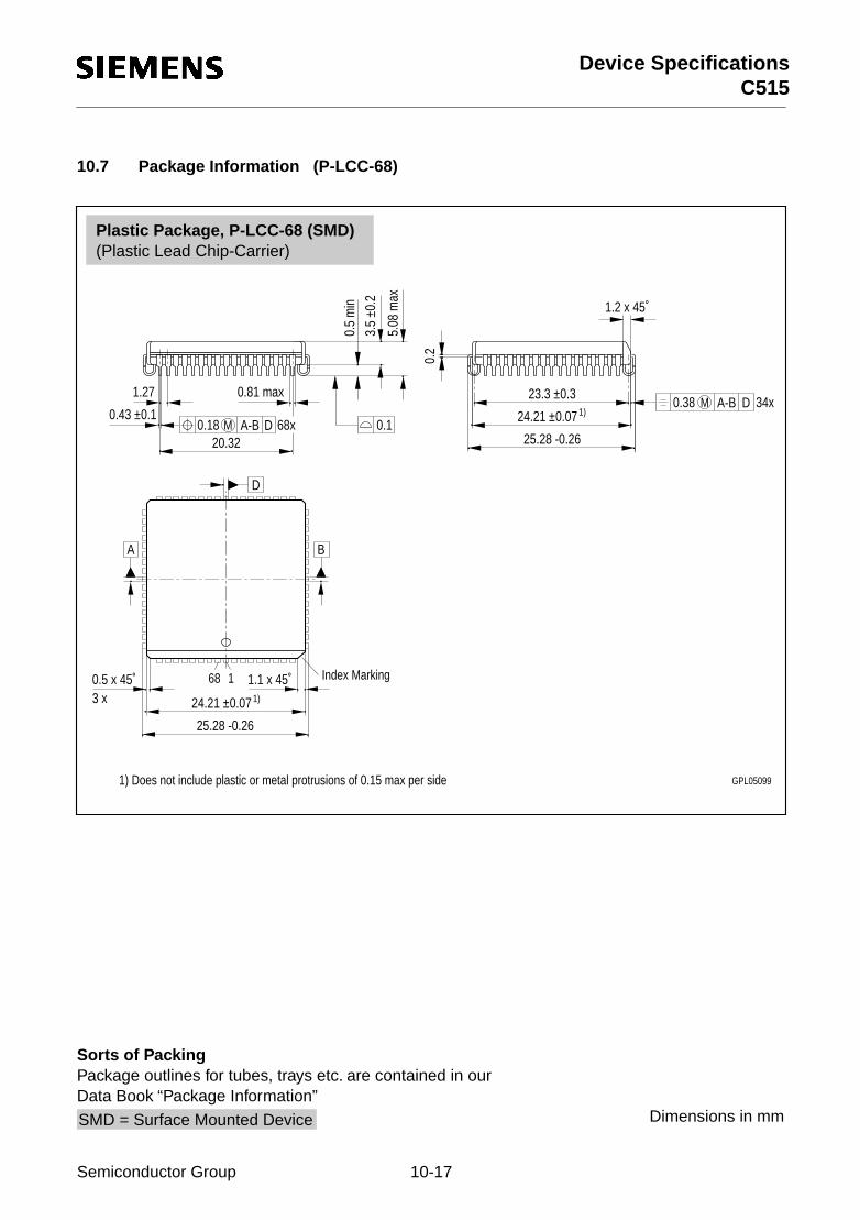
Device SpecificationsC515
10.7 Package Information (P-LCC-68)
GPL05099
0.81 max1.27
0.43 ±0.10.18 M 68xDA-B
20.320.1
5.08
max
3.5
±0.2
0.5
min
0.2
1.2 x 45˚
23.3 ±0.3
24.21 ±0.07
25.28 -0.26
1)0.38 M DA-B 34x
A B
D
1680.5 x 45˚3 x 24.21 ±0.07 1)
25.28 -0.26
1.1 x 45˚ Index Marking
1) Does not include plastic or metal protrusions of 0.15 max per side
Plastic Package, P-LCC-68 (SMD)(Plastic Lead Chip-Carrier)
Sorts of PackingPackage outlines for tubes, trays etc. are contained in our Data Book “Package Information”
Dimensions in mmSMD = Surface Mounted Device
Semiconductor Group 10-17

Device SpecificationsC515
10.8 Package Information (P-MQFP-80)
0.650.3
12.350.1
2 2.45
max
180
Index Marking
17.2
14
0.25
min
+0.1
0.88
1)
0.6x45˚
1) Does not include plastic or metal protrusions of 0.25 max per side
A-B0.2 HD 4xA-B0.2 D 80x
A B
D
C0.12 80xDA-BM
C1)
14 17.2
-0.0
5
H
7˚m
ax-0.0
2+0
.08
0.15
±0.08
GP
M05
249
Plastic Package, P-MQFP-80-1 (SMD)(Plastic Metric Quad Flat Package)
Sorts of PackingPackage outlines for tubes, trays etc. are contained in our Data Book “Package Information”
Dimensions in mmSMD = Surface Mounted Device
Semiconductor Group 10-18

IndexC515
11 Index
AA/D converter . . . . . . . . . . . . . . .6-57–6-68
Conversion timing . . . . . . . . . .6-66–6-68General operation . . . . . . . . . . . . . . 6-57Programmable reference voltages . 6-62–
6-65Registers . . . . . . . . . . . . . . . . .6-59–6-61
A/D converter characteristics . . . . . . . 10-5Absolute maximum ratings . . . . . . . . . 10-1AC . . . . . . . . . . . . . . . . . . . . . . . . . .2-3, 3-7AC characteristics . . . . . . . . . . .10-6–10-16
16 MHz timing . . . . . . . . . . . . .10-6–10-724 MHz timing . . . . . . . . . . . . .10-8–10-9CLKOUT timing . . . . . . . . . . . . . . . 10-13Data memory read cycle . . . . . . . . 10-11Data memory write cycle . . . . . . . . 10-12External clock timing . . . . . . . . . . . 10-13Program memory read cycle . . . . . 10-10ROM verification mode 1 . . . . . . . . 10-14ROM verification mode 2 . . . . . . . . 10-15
AC TestingFloat waveforms . . . . . . . . . . . . . . 10-16Input/output waveforms . . . . . . . . . 10-16
ACC . . . . . . . . . . . . . . . . . . . . . . . . .3-4, 3-7ADCON . . . . . 3-4, 3-5, 3-7, 5-6, 6-44, 6-59ADDAT . . . . . . . . . . . . . . . . . 3-4, 3-7, 6-60ADM . . . . . . . . . . . . . . . . . . . . . . .3-7, 6-59ALE signal . . . . . . . . . . . . . . . . . . . . . . . 4-4
BB . . . . . . . . . . . . . . . . . . . . . . . . . . .3-4, 3-7Basic CPU timing . . . . . . . . . . . . . . . . . 2-4BD . . . . . . . . . . . . . . . . . . . . . . . . .3-7, 6-44Block diagram . . . . . . . . . . . . . . . . . . . . 2-1BSY . . . . . . . . . . . . . . . . . . . . . . . .3-7, 6-59
CC/T . . . . . . . . . . . . . . . . . . . . . . . . .3-6, 6-17CCEN . . . . . . . . . . . . . . . . . . 3-4, 3-7, 6-28CCH1 . . . . . . . . . . . . . . . . . . . 3-4, 3-7, 6-31CCH2 . . . . . . . . . . . . . . . . . . . 3-4, 3-7, 6-31CCH3 . . . . . . . . . . . . . . . . . . . 3-4, 3-7, 6-31CCL1 . . . . . . . . . . . . . . . . . . . . . . .3-4, 6-31CCL2 . . . . . . . . . . . . . . . . . . . 3-4, 3-7, 6-31CCL3 . . . . . . . . . . . . . . . . . . . 3-4, 3-7, 6-31CLK . . . . . . . . . . . . . . . . . . . . . . . . .3-7, 5-6CLKOUT . . . . . . . . . . . . . . . . . . . . .3-6, 5-6
COCAH0 . . . . . . . . . . . . . . . . . . . . 3-7, 6-28COCAH1 . . . . . . . . . . . . . . . . . . . . 3-7, 6-28COCAH2 . . . . . . . . . . . . . . . . . . . . 3-7, 6-28COCAH3 . . . . . . . . . . . . . . . . . . . . 3-7, 6-28COCAL0 . . . . . . . . . . . . . . . . . . . . 3-7, 6-28COCAL1 . . . . . . . . . . . . . . . . . . . . 3-7, 6-28COCAL2 . . . . . . . . . . . . . . . . . . . . 3-7, 6-28COCAL3 . . . . . . . . . . . . . . . . . . . . 3-7, 6-28CPU
Accumulator . . . . . . . . . . . . . . . . . . . .2-2B register . . . . . . . . . . . . . . . . . . . . . . .2-3Basic timing . . . . . . . . . . . . . . . . . . . . .2-4Fetch/execute diagram . . . . . . . . . . . .2-5Functionality . . . . . . . . . . . . . . . . . . . .2-2Program status word . . . . . . . . . . . . . .2-2Stack pointer . . . . . . . . . . . . . . . . . . . .2-3
CPU timing . . . . . . . . . . . . . . . . . . . . . . .2-5CRCH . . . . . . . . . . . . . . . . . . 3-4, 3-7, 6-26CRCL . . . . . . . . . . . . . . . . . . 3-4, 3-7, 6-26CY . . . . . . . . . . . . . . . . . . . . . . . . . . 2-3, 3-7
DDAPR . . . . . . . . . . . . . . . . . . 3-4, 3-7, 6-62DC characteristics . . . . . . . . . . . . 10-2–10-4Device characteristics . . . . . . . . 10-1–10-18DPH . . . . . . . . . . . . . . . . . . . . . . . . 3-4, 3-6DPL . . . . . . . . . . . . . . . . . . . . . . . . . 3-4, 3-6
EEADC . . . . . . . . . . . . . . . . . . 3-6, 6-61, 7-5EAL . . . . . . . . . . . . . . . . . . . . . . . . . 3-6, 7-4EALE . . . . . . . . . . . . . . . . . . . . . . . . . . . .4-4Emulation concept . . . . . . . . . . . . . . . . .4-5ES . . . . . . . . . . . . . . . . . . . . . . . . . . 3-6, 7-4ET0 . . . . . . . . . . . . . . . . . . . . . . . . . 3-6, 7-4ET1 . . . . . . . . . . . . . . . . . . . . . . . . . 3-6, 7-4ET2 . . . . . . . . . . . . . . . . . . . . 3-6, 6-27, 7-4EX0 . . . . . . . . . . . . . . . . . . . . . . . . . 3-6, 7-4EX1 . . . . . . . . . . . . . . . . . . . . . . . . . 3-6, 7-4EX2 . . . . . . . . . . . . . . . . . . . . . . . . . 3-6, 7-5EX3 . . . . . . . . . . . . . . . . . . . . . . . . . 3-6, 7-5EX4 . . . . . . . . . . . . . . . . . . . . . . . . . 3-6, 7-5EX5 . . . . . . . . . . . . . . . . . . . . . . . . . 3-6, 7-5EX6 . . . . . . . . . . . . . . . . . . . . . . . . . 3-6, 7-5Execution of instructions . . . . . . . . . . . . .2-4EXEN2 . . . . . . . . . . . . . . . . . 3-6, 6-27, 7-5EXF2 . . . . . . . . . . . . . . . . . . . 3-7, 6-27, 7-8External bus interface . . . . . . . . . . . 4-1–4-4
ALE signal . . . . . . . . . . . . . . . . . . . . . .4-4
Semiconductor Group 11-1

IndexC515
Overlapping of data/program memory 4-3Program memory access . . . . . . . . . . 4-3Program/data memory timing . . . . . . 4-2PSEN signal . . . . . . . . . . . . . . . . . . . . 4-3Role of P0 and P2 . . . . . . . . . . . . . . . 4-1
FF0 . . . . . . . . . . . . . . . . . . . . . . . . . .2-3, 3-7F1 . . . . . . . . . . . . . . . . . . . . . . . . . .2-3, 3-7Fail save mechanisms . . . . . . . . . . .8-1–8-4Features . . . . . . . . . . . . . . . . . . . . . . . . 1-2Functional units . . . . . . . . . . . . . . . . . . . 1-1Fundamental structure . . . . . . . . . . . . . 2-1
GGATE . . . . . . . . . . . . . . . . . . . . . . .3-6, 6-17GF0 . . . . . . . . . . . . . . . . . . . . . . . . .3-6, 9-2GF1 . . . . . . . . . . . . . . . . . . . . . . . . .3-6, 9-2
HHardware reset . . . . . . . . . . . . . . . . . . . 5-1
II/O ports . . . . . . . . . . . . . . . . . . . . .6-1–6-13I2FR . . . . . . . . . . . . . . . . . . . . . . . . .3-7, 7-7I3FR . . . . . . . . . . . . . . . . . . . . 3-7, 6-25, 7-7IADC . . . . . . . . . . . . . . . . . . . 3-7, 6-61, 7-8IDLE . . . . . . . . . . . . . . . . . . . . . . . .3-6, 9-2Idle mode . . . . . . . . . . . . . . . . . . . . .9-3–9-4IDLS . . . . . . . . . . . . . . . . . . . . . . . .3-6, 9-2IE0 . . . . . . . . . . . . . . . . . . . . . . . . . .3-6, 7-6IE1 . . . . . . . . . . . . . . . . . . . . . . . . . .3-6, 7-6IEN0 . . . . . . . . 3-4, 3-5, 3-6, 6-27, 7-4, 8-4IEN1 . . . .3-4, 3-5, 3-6, 6-27, 6-61, 7-5, 8-4IEX2 . . . . . . . . . . . . . . . . . . . . . . . . .3-7, 7-8IEX3 . . . . . . . . . . . . . . . . . . . . . . . . .3-7, 7-8IEX4 . . . . . . . . . . . . . . . . . . . . . . . . .3-7, 7-8IEX5 . . . . . . . . . . . . . . . . . . . . . . . . .3-7, 7-8IEX6 . . . . . . . . . . . . . . . . . . . . . 3-7, 7-8, 7-8INT0 . . . . . . . . . . . . . . . . . . . . . . . . . . . . 3-6INT1 . . . . . . . . . . . . . . . . . . . . . . . . . . . . 3-6INT2 . . . . . . . . . . . . . . . . . . . . . . . . . . . . 3-6INT3 . . . . . . . . . . . . . . . . . . . . . . . . . . . . 3-6INT4 . . . . . . . . . . . . . . . . . . . . . . . . . . . . 3-6INT5 . . . . . . . . . . . . . . . . . . . . . . . . . . . . 3-6INT6 . . . . . . . . . . . . . . . . . . . . . . . . . . . . 3-6Interrupt system . . . . . . . . . . . . . . .7-1–7-17Interrupts
Block diagram . . . . . . . . . . . . . . .7-2–7-3Enable registers . . . . . . . . . . . . . .7-4–7-5
External interrupts . . . . . . . . . . . . . . .7-15Handling procedure . . . . . . . . . . . . . .7-13Priority registers . . . . . . . . . . . . . . . .7-11Priority within level structure . . . . . . .7-12Request flags . . . . . . . . . . . . . . 7-6–7-10Response time . . . . . . . . . . . . . . . . .7-17Sources and vector addresses . . . . .7-14
IP0 . . . . . . . . . . . . . . . . . 3-5, 3-6, 7-11, 8-4IP1 . . . . . . . . . . . . . . . . . . . . 3-4, 3-6, 7-11IRCON . . . . . . . . . 3-4, 3-7, 6-27, 6-61, 7-8IT0 . . . . . . . . . . . . . . . . . . . . . . . . . . 3-6, 7-6IT1 . . . . . . . . . . . . . . . . . . . . . . . . . . 3-6, 7-6
LLogic symbol . . . . . . . . . . . . . . . . . . . . . .1-3
MM0 . . . . . . . . . . . . . . . . . . . . . . . . . 3-6, 6-17M1 . . . . . . . . . . . . . . . . . . . . . . . . . 3-6, 6-17Memory organization . . . . . . . . . . . 3-1–3-2
Data memory . . . . . . . . . . . . . . . . . . . .3-2General purpose registers . . . . . . . . . .3-2Memory map . . . . . . . . . . . . . . . . . . . .3-1Program memory . . . . . . . . . . . . . . . .3-2
MX0 . . . . . . . . . . . . . . . . . . . . . . . . . . . .3-7MX1 . . . . . . . . . . . . . . . . . . . . . . . . . . . .3-7MX2 . . . . . . . . . . . . . . . . . . . . . . . . . . . .3-7MX2-0 . . . . . . . . . . . . . . . . . . . . . . . . . .6-59
OOscillator operation . . . . . . . . . . . . . 5-4–5-5
External clock source . . . . . . . . . . . . .5-5On-chip oscillator circuitry . . . . . . . . . .5-5Recommended oscillator circuit . . . . .5-4
OV . . . . . . . . . . . . . . . . . . . . . . . . . . 2-3, 3-7P
P . . . . . . . . . . . . . . . . . . . . . . . . . . . 2-3, 3-7P0 . . . . . . . . . . . . . . . . . . . . . . . . . . 3-4, 3-6P1 . . . . . . . . . . . . . . . . . . . . . . . . . . 3-5, 3-6P2 . . . . . . . . . . . . . . . . . . . . . . . . . . 3-5, 3-6P3 . . . . . . . . . . . . . . . . . . . . . . . . . . 3-5, 3-6P4 . . . . . . . . . . . . . . . . . . . . . . . . . . 3-5, 3-7P5 . . . . . . . . . . . . . . . . . . . . . . . . . . 3-5, 3-7P6 . . . . . . . . . . . . . . . . . . . . . . . . . . 3-5, 3-7Package information (P-LCC-68) . . . .10-17Package information (P-MQFP-80) . .10-18Parallel I/O . . . . . . . . . . . . . . . . . . 6-1–6-13PCON . . . . . . . . . . . . . . . 3-5, 3-6, 6-44, 9-2PDE . . . . . . . . . . . . . . . . . . . . . . . . 3-6, 9-2
Semiconductor Group 11-2

IndexC515
PDS . . . . . . . . . . . . . . . . . . . . . . . . .3-6, 9-2Pin configuration . . . . . . . . . . . . . . . . . . 1-4
P-MQFP-80 package . . . . . . . . . .1-4, 1-5Pin definitions and functions . . . . .1-6–1-10Ports . . . . . . . . . . . . . . . . . . . . . . .6-1–6-13
Alternate functions . . . . . . . . . . . . . . . 6-2Loading and interfacing . . . . . . . . . . 6-12Output driver circuitry . . . . . . . . .6-9–6-10Output/input sample timing . . . . . . . 6-11Read-modify-write operation . . . . . . 6-13Types and structures . . . . . . . . . . . . . 6-1
Port 0 circuitry . . . . . . . . . . . . . . . . 6-5Port 1/3/4/5 circuitry . . . . . . . . . . . . 6-6Port 2 circuitry . . . . . . . . . . . . . . . . 6-7Standard I/O port circuitry . . . .6-3–6-4
Power down mode . . . . . . . . . . . . . . . . . 9-6Entry procedure . . . . . . . . . . . . . . . . . 9-6Exit procedure . . . . . . . . . . . . . . . . . . 9-6
Power saving modes . . . . . . . . . . . .9-1–9-7Control register . . . . . . . . . . . . . . . . . 9-2Hardware enable . . . . . . . . . . . . . . . . 9-1Idle mode . . . . . . . . . . . . . . . . . . .9-3–9-4Power down mode . . . . . . . . . . . . . . . 9-6Slow down mode . . . . . . . . . . . . . . . . 9-5State of pins . . . . . . . . . . . . . . . . . . . . 9-7
Power supply current . . . . . . . . . .10-3–10-4PSEN signal . . . . . . . . . . . . . . . . . . . . . 4-3PSW . . . . . . . . . . . . . . . . . . . . 2-3, 3-4, 3-7
RRB8 . . . . . . . . . . . . . . . . . . . . . . . .3-6, 6-43RD . . . . . . . . . . . . . . . . . . . . . . . . . . . . . 3-6Recommended oscillator circuits . . . . 10-16REN . . . . . . . . . . . . . . . . . . . . . . . .3-6, 6-43Reset . . . . . . . . . . . . . . . . . . . . . . . .5-1–5-3
Hardware reset timing . . . . . . . . . . . . 5-3Reset circuitries . . . . . . . . . . . . . . . . . 5-2
RI . . . . . . . . . . . . . . . . . . . . . 3-6, 6-43, 7-10ROM protection . . . . . . . . . . . . . . . .4-6–4-8
Protected ROM mode . . . . . . . . . . . . 4-7Protected ROM verification example . 4-8Protected ROM verify timing . . . . . . . 4-7Unprotected ROM mode . . . . . . . . . . 4-6Unprotected ROM verify timing . . . . . 4-6
RS0 . . . . . . . . . . . . . . . . . . . . . . . . .2-3, 3-7RS1 . . . . . . . . . . . . . . . . . . . . . . . . .2-3, 3-7RxD . . . . . . . . . . . . . . . . . . . . . . . .3-6, 6-41
SSBUF . . . . . . . . . . . . . . . . . . 3-5, 3-6, 6-43SCON . . . . . . . . . . 3-4, 3-5, 3-6, 6-43, 7-10SD . . . . . . . . . . . . . . . . . . . . . . . . . . 3-6, 9-2Serial interface (USART) . . . . . . 6-41–6-56
Baudrate generation . . . . . . . . . . . . .6-44with internal baud rate generator . .6-46with timer 1 . . . . . . . . . . . . . . . . . .6-46
Multiprocessor communication . . . . .6-42Operating mode 0 . . . . . . . . . . 6-48–6-50Operating mode 1 . . . . . . . . . . 6-51–6-53Operating mode 2 and 3 . . . . . 6-54–6-56Registers . . . . . . . . . . . . . . . . . 6-42–6-43
Slow down mode . . . . . . . . . . . . . . . . . .9-5SM0 . . . . . . . . . . . . . . . . . . . . . . . 3-6, 6-43SM1 . . . . . . . . . . . . . . . . . . 3-6, 6-43, 6-43SM2 . . . . . . . . . . . . . . . . . . . . . . . 3-6, 6-43SMOD . . . . . . . . . . . . . . . . . . . . . . 3-6, 6-44SP . . . . . . . . . . . . . . . . . . . . . . . . . . 3-4, 3-6Special Function Registers . . . . . . . . . . .3-3
Table - address ordered . . . . . . . 3-6–3-7Table - functional order . . . . . . . . 3-4–3-5
SWDT . . . . . . . . . . . . . . . . . . . . . . . 3-6, 8-4SYSCON . . . . . . . . . . . . . . . . . 3-4, 3-6, 4-4System clock output . . . . . . . . . . . . 5-6–5-7
TT0 . . . . . . . . . . . . . . . . . . . . . . . . . . . . . .3-6T1 . . . . . . . . . . . . . . . . . . . . . . . . . . . . . .3-6T2 . . . . . . . . . . . . . . . . . . . . . . . . . . . . . .3-6T2CM . . . . . . . . . . . . . . . . . . . . . . 3-7, 6-25T2CON . . . . . . . . . . 3-4, 3-5, 3-7, 6-25, 7-7T2EX . . . . . . . . . . . . . . . . . . . . . . . . . . . .3-6T2I0 . . . . . . . . . . . . . . . . . . . . . . . . 3-7, 6-25T2I1 . . . . . . . . . . . . . . . . . . . . . . . . 3-7, 6-25T2PS . . . . . . . . . . . . . . . . . . . . . . . 3-7, 6-25T2R0 . . . . . . . . . . . . . . . . . . . . . . . 3-7, 6-25T2R1 . . . . . . . . . . . . . . . . . . . . . . . 3-7, 6-25TB8 . . . . . . . . . . . . . . . . . . . . . . . . 3-6, 6-43TCON . . . . . . . . . . . . . . . 3-4, 3-6, 6-16, 7-6TF0 . . . . . . . . . . . . . . . . . . . . 3-6, 6-16, 7-6TF1 . . . . . . . . . . . . . . . . . . . . 3-6, 6-16, 7-6TF2 . . . . . . . . . . . . . . . . . . . . 3-7, 6-27, 7-8TH0 . . . . . . . . . . . . . . . . . . . . 3-4, 3-6, 6-15TH1 . . . . . . . . . . . . . . . . . . . . 3-4, 3-6, 6-15TH2 . . . . . . . . . . . . . . . . . . . . 3-4, 3-7, 6-26TI . . . . . . . . . . . . . . . . . . . . . 3-6, 6-43, 7-10Timer/counter . . . . . . . . . . . . . . . 6-14–6-40
Semiconductor Group 11-3

IndexC515
Timer/counter 0 and 1 . . . . . . .6-14–6-21Mode 0, 13-bit timer/counter . . . . 6-18Mode 1, 16-bit timer/counter . . . . 6-19Mode 2, 8-bit rel. timer/counter . . 6-20Mode 3, two 8-bit timer/counter . . 6-21Registers . . . . . . . . . . . . . . .6-15–6-17
Timer/counter 2 . . . . . . . . . . . .6-22–6-40Alternate port functions . . . . . . . . 6-22Block diagram . . . . . . . . . . . . . . . 6-23Capture function . . . . . . . . . .6-39–6-40Compare function . . . . . . . . .6-31–6-36Compare mode 0 . . . . . . . . .6-31–6-34Compare mode 1 . . . . . . . . .6-35–6-36Compare mode interrupts . . . . . . 6-37General operation . . . . . . . . . . . . 6-29Registers . . . . . . . . . . . . . . .6-24–6-28Reload mode . . . . . . . . . . . . . . . . 6-30
TimingsCLKOUT timing . . . . . . . . . . . . . . . 10-13Data memory read cycle . . . . . . . . 10-11Data memory write cycle . . . . . . . . 10-12External clock timing . . . . . . . . . . . 10-13Program memory read cycle . . . . . 10-10ROM verification mode 1 . . . . . . . . 10-14ROM verification mode 2 . . . . . . . . 10-15
TL0 . . . . . . . . . . . . . . . . . . . . 3-4, 3-6, 6-15TL1 . . . . . . . . . . . . . . . . . . . . 3-4, 3-6, 6-15TL2 . . . . . . . . . . . . . . . . . . . . 3-5, 3-7, 6-26TMOD . . . . . . . . . . . . . . . . . . 3-4, 3-6, 6-17TR0 . . . . . . . . . . . . . . . . . . . . . . . .3-6, 6-16TR1 . . . . . . . . . . . . . . . . . . . . . . . .3-6, 6-16TxD . . . . . . . . . . . . . . . . . . . . . . . .3-6, 6-41
WWatchdog timer . . . . . . . . . . . . . . . .8-1–8-4
Block diagram . . . . . . . . . . . . . . . . . . 8-3Control and status flags . . . . . . . . . . . 8-4General operation . . . . . . . . . . . . . . . 8-1Refreshing of the WDT . . . . . . . . . . . 8-2Reset operation . . . . . . . . . . . . . . . . . 8-2Starting of the WDT . . . . . . . . . . . . . . 8-1
WDT . . . . . . . . . . . . . . . . . . . . . . . .3-6, 8-4WDTS . . . . . . . . . . . . . . . . . . . . . . .3-6, 8-4WR . . . . . . . . . . . . . . . . . . . . . . . . . . . . 3-6
Semiconductor Group 11-4