Embed Size (px)
Citation preview

1
INF5490 RF MEMS
L13: RF MEMS capacitors
S2008, Oddvar SøråsenDepartment of Informatics, UoO

2
Today’s lecture• Passive components in RF circuits
– Capacitors, C– Inductors, L
• Tunable RF MEMS capacitors– Vertical tunable capacitors– Lateral tunable capacitors– Thermal tunable MEMS capacitance– Piezoelectric actuator tunable capacitors– Tuning by changing of dielectric material
• RF MEMS capacitance banks

3
Passive components in RF circuits
• MEMS capacitors and inductors– Relevant as replacements for traditional ”off-chip”
passive components– Tuneability and programability are desired
• MEMS capacitors– Simple, tunable capacitances
• = varactor (”variable reactor”)– Programable capacitance banks with fixed C
• MEMS inductors (L14)– Simple, fixed inductors– Programable inductance banks with fixed L

4
Use of tunable capacitors
• VCO = ”Voltage controlled oscillator”– Value of C determines the frequency– Voltage tuned– VCO has strict requirements on
• Stability• Low phase noise• Wide frequency bandwidth
• Tunable filters• Tunable network• Impedance matching• Phase shifters

5
MEMS compete with commercial semiconductor technologies
• Many discrete Si and GaAs varactors exist– 30 GHz– Ex. Q = 30-60 for 0.5-5 GHz (SiGe)– MEMS varactors not mature enough to replace GaAs
varactors, especially for frequencies below 5 GHz• MEMS varactors have not developed as fast as
MEMS switches– But: is the RF MEMS component closest to
commercial applications– Relative mature technology– Already, many replacements using MEMS have been
demonstrated, DC 100 GHz

6
Typical characteristics for MEMS varactors
• + Potentially high Q-values– High Q-value (>100) over a wide frequency band
• Q = 100 – 400 for mm-frequencies• + Simplicity, compared with alternative
technologies• + Capable of sustaining large RF voltage• + Low cost fabrication on glass, ceramic, high-
resistivity Si-substrate – Ex. ”low-cost” 3 – 60 GHz tunable networks and filters
• + More reliable• + Simple and low-cost packaging

7
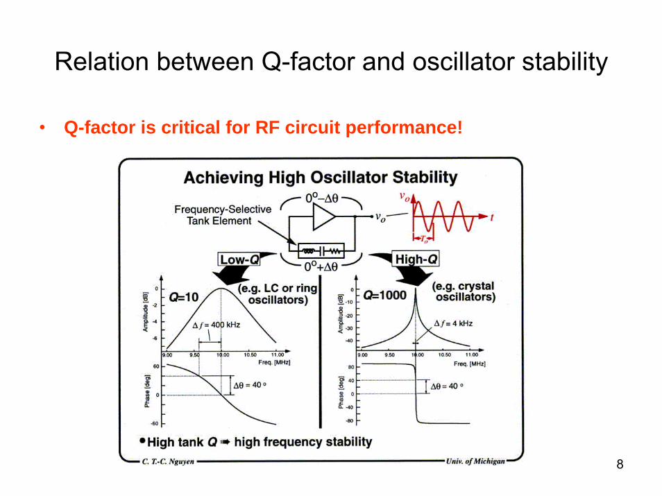
Why high Q-values?
• Q-factor characterizes loss due to power dissipation in elements
• Q should be as high as possible to reduce Insertion loss
8
Relation between Q-factor and oscillator stability
• Q-factor is critical for RF circuit performance!

9
Equivalent circuit for capacitor• At high frequency
inductance– has a characteristic
self resonance frequency
– Inductance should be as low as possible so the self resonance frequency is much higher than the frequency used in normal operation

10
Impedance and Q-factor for a discrete capacitor
Q-factor given for ωL<<1/ωC
Calculations shown next Rebeiz

11
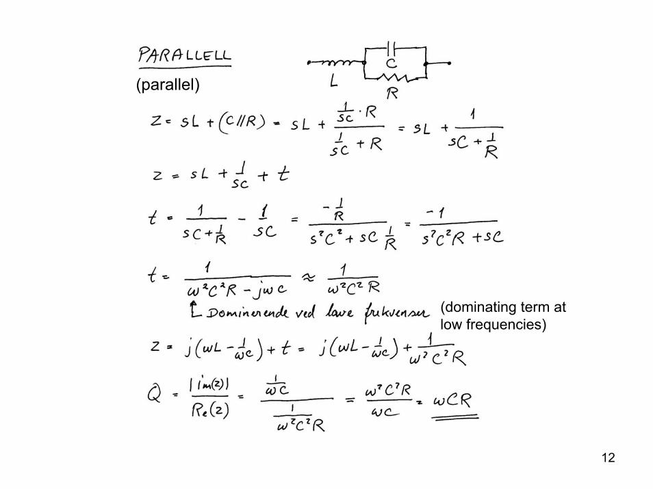
(series)
(Self resonance)
Below self resonance)
12
(parallel)
(dominating term at low frequencies)

13
Challenges for RF MEMS capacitors
• ÷ Tuning ratio for MEMS varactors is small– 1.2 – 2.5– For semiconductor varactors: 4 – 6– Obtain required Tuning Ratio (TR)
• Definition TR: • Should be > 2
• ÷ MEMS is sensitive to various noise effectspresent for low spring constant, k– Low k is desired for 3 – 5 V applications– Is a challenge due to
• Acceleration, RF power self actuation, noise effects
minmax CC

14
Parallel plate capacitor
• Basic equations– Q = V C, I = C dV/dt– C = ε A / g
• NB! C generally tuned by 3 parameters– g, gap– A, area– ε, dielectric constant

15
Tunable RF MEMS capacitors• Electrostatic actuation is a dominating mechanism for
tuning– Low power consumption, simple
• Vertical electrostatic displacement– Tuning the gap (non-linear change) in parallel plate capacitor
• 2-plate capacitance• 3-plate capacitance• Double air-gap capacitance• Other examples
• Horizontal (lateral) displacement– Tuning of area (linear change)
• Thermal tunable MEMS capacitance• Piezoelectric actuator tunable capacitance• Tuning by change of dielectric material

16
Two-plate tunable MEMS capacitance
• Young & Boser, Berkeley• Gap-tuning• One plate can move by
electrostatic actuation• Equilibrium between
elastic and electrical forces

17
Calculation of TR for 2-plate capacitance
1
Theoretical TR = 150%. Limited by the pull-in effect

18
Young & Bover, Berkeley
• Etching a hole in capacitance plate– For decreased squeezed-film
damping– Positive for ”release”-step in
the process
Varadan

19
Implementation
• Typical features for a Berkeley implementation
• Surface micromachining– 2 metal layers + Al
gnd-plane
LTO = Low temperature oxide

20
3-plate tunable MEMS capacitance
• TR can be increased by introducing a 3rd plate– A. Dec & K. Suyama: ”Micromachined Electro-Mechanically
Tunable Capacitors and Their Applications to RF IC´s” 1998. Columbia University

21
Calculating TR for 3-plate
TR = 200%, e.g.: can be tuned 100%

22
Demonstrated values,Dec & Suyama:

23Rebeiz:Dec & Suyama

24
Dec & Suyama, contd.
• Process– Standard 3-layer poly
surface micromachining (MUMP´s) with HF etching and ”supercritical drying”
– Poly often used as parallel plate due to superior mechanical properties instead of Al (in spite of Al having better conductivity)

25
Dec & Suyama, ex.2
Rebeiz

26
Double air-gap capacitance
• J. Zou et al, 2000, Univ of Illinois
• Why double air-gap?– Increase TR
• Eliminate pull-in effect– May deflect down to 1/3 d2
before pull-in – TR may increase significantly
if 1/3 *d2 > d1
• Eg. centre electrode can be fully deflected without pull-in!

27
Univ of Illinois, contd.

28
Univ of Illinois, contd.Simplified fabrication process
- Cu as sacrificial layer- Metals: gold & permaloy (Ni-Fe)- Air-gap: d1 = 2 µm, d3 = 3 µm

29
Ex. from Univ of Michigan
Rebeiz
30
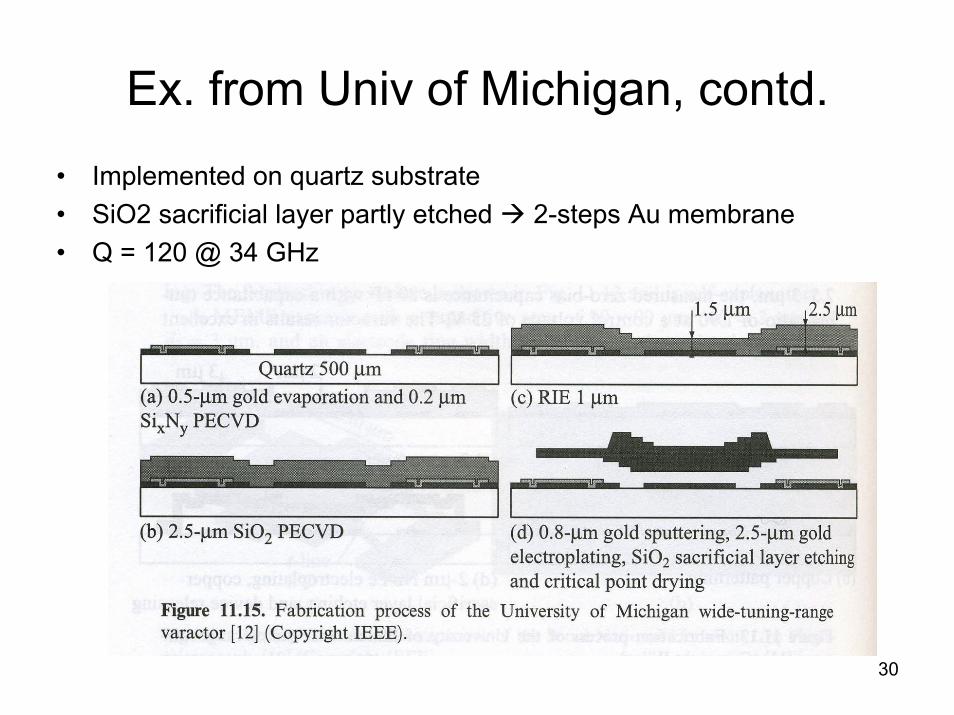
Ex. from Univ of Michigan, contd.
• Implemented on quartz substrate• SiO2 sacrificial layer partly etched 2-steps Au membrane• Q = 120 @ 34 GHz

31
Univ of Michigan, discrete 2-valued

32
Different segments with multi-gap. May be tuned to 2 or 3 levels. Hystereses properties
Ionescu, EPFL: H. Nieminen et al (Nokia)

33
Working principle:

34
”Zipper” capacitance
• Ex. zipper cantilever capacitance
• Design and fabrication at Columbia University– Long, thin beam deflected
gradually from one edge– Small capacitances added
in parallel

35
Ex. from MIT
Softest near edge
Rebeiz

36
Univ of Colorado, Boulder
• Digitally controlled individual capacitances• Has individual plates that may be actuated
sequentially
Varadan

37
Univ of Colorado, Boulder
Each ”plate” coupled withdifferent width of beam, eg.different spring constant foreach part
Standard MUMP´s process (poly-Si and gold), alumina-substrate
Electrostatic actuation V= 30 VTR = 4 : 1Q = 140 @ 750 MHz

38
Elevated platform capacitance
• L. Fan et al, 1998– One of the electrodes may be
elevated to several hundred micrometers above the substrate
• 250 µm elevation, TR 2400%• ÷ Fine tuning difficult
• Uses actuators pushing the structure together– ”Scratch drive actuator”– Must implement hinges

39Ionescu, EPFL

40
Self actuation
• Design parallel plate capacitances to handle RF power – AC applied over the RF MEMS capacitance
• RF frequency does not modulate C-value– BUT, RMS-value of RF-signal will influence C and
can induce pull-in by self actuation
• Capacitances for gap-tuning has limited RF power handling capability due to small electrode gap– Decrease distance RF breakdown

41
Lateral tunable capacitors
• Horizontal displacement– C can be tuned by changing the area, C = ε A / g– + No theoretical limit for TR– + Pull-in effect avoided– ÷ Photolithography determines precision of
dimensions– ÷ More complicated suspension structures?
• Make sure that the movable structure is suspended!
• Comb structure is common

42Ionescu, EPFL: J. J. Yao et al, Rockwell

43
Simple comb structure
• Ex. from Rockwell Science Center – Inter-digital tunable MEMS capacitance– One set of combs is stationary, the other set can be
moved– Gap is not changing– Length of comb and finger length limit tuning range– Can be tuned by an electrostatic micro motor or by
applying different actuation voltages

44
Rockwell Science Center, forts.
Ex. of tuning
VS = RF HS = tuning
Varadan

45
Rockwell Science Center, contd.
Rebeiz

46
Rockwell Science Center, contd.
Rebeiz

47
Thermal tunable parallel-plate MEMS capacitance
• Use hot and cold arms– A high resistivity arm will be hotter and deform more
• Differential thermal expansion
• Challenges with this technology – Power dissipation– Low speed– But removes the pull-in limitation!

48
Univ of Colorado
Z. Feng et al, Univ of Colorado: Design and Modeling of RF MEMS Tunable Capacitors Using Electro-thermal Actuators
Rebeiz

49Temperature gradient causes a vertical displacement
Ionescu, EPFL

50
Electro-thermal tuning
Varadan

51
Variable capacitors in CMOS-MEMS

52
CMOS-MEMS:Lateral displacement due to differentstress gradients in metal anddielectrics

Different thermalexpansion coefficientsfor Al and dielectricscauses movement uponheating
53

54Carnegie Mellon University

55Carnegie Mellon University

56
Vertical curling upon post-CMOS release
The effect can be usedfor making variable C
National Chung Hsing Univ,Taiwan, Dai et al

57
Piezoelectric tuningA bias voltage causes the capacitor plate to move vertically
+ Low drive-voltage+ Linear tuning of capacitance
Two of the beam lengths increase
Rebeiz

58Rebeiz

59
Dielectric tunable capacitances
• Change the material properties between plates– DC bias voltage can
change electrical properties
• Dielectric layer• Dielectric constant, ε
– Ferro-electric thin-films, Var fig. 4.48

60
University of Michigan
Movable dielectric membranebetween fixed plates, - maskingthe effective area
Rebeiz

61
Univ of Micigan, explanation
• Principle: both top and bottom are rigid• Tuning by a movable dielectric membrane
(high-k = ε) that is electrostatic actuated• Performance parameters
– IC compatible technology (<200 ° C), post CMOS– Electroplated metal + surface micromachining– Movable dielectric Nitride membrane– No pull-in effect– Low actuation voltage < 10 V with k = 0.187 N/m– TR = 40%– Q = 218 @ 1 GHz for C = 1.14 pF design (maybe the
highest Q published!)

62
Univ of Micigan, contd.
Rebeiz

63
RF MEMS capacitance banks
• Use of programmable capacitance banks– Use an ”array” of fixed capacitances– Connect to the desired C-value– MEMS switches used for connecting– Can be programmed using a digital signal
– Both series and shunt configurations are possible

64Ionescu, EPFL

65
Eliminate influence of thermal stress
• One example• H. Nieminen et al: ”Design of a Temperature-
Stable RF MEMS Capacitor, J MMSyst, vol 13, no 5, 2004:
• Design capacitance into a frame-structure• Use frame to compensate the thermal induced
stress• Anchor the capacitance in such a way that when
the frame is deformed, minimal stress is induced on the capacitance itself
– Ex. corners displace very little– Anchor the capacitance in the corners!

66

67