Embed Size (px)
Citation preview

1
INDUSTRIAL TRAINING INSTITUTE, ................................... F: TRG: 05
LIST OF INFORMATION
TRADE: ELECTRONIC MECHENIC NAME OF S.I.:
SEMESTER NO.‐ 3 SYLLABUS YEAR: 2017 (NSQF)
SR. NO.
NAME OF LESSON TIME (MIN.)
SY. WEEK NO.
ACTUAL WEEK NO.
1 Block diagram advantages and application of DSO/CRO.
50 Min. 1
2 Differentiate a CRO with DSO 50 Min. 1
3 block diagram of function generator 50 Min. 1
4 Introduction to SMD components. 50 Min. 2
5 Advantage of SMD components over conventional lead components
50 Min. 2
6 Soldering of SMD assemblies. 50 Min. 2
7 Introduction to Surface Mount Technology (SMT). 50 Min. 3
8 Soldering of SMD assemblies. 50 Min. 3
9 Identification of PGA Packages and their Soldering/De‐soldering
50 Min. 3
10 Cold/continuity of PCB's Identification of lose/dry solders, broken tracks on printed wiring assembly
50 Min. 4
11 Introduction to solder paste (flux) 50 Min. 4
12 Introduction, Prevention and handling of Static charges.
50 Min. 5
13 Introduction to crimping, wire wrapping, conductive adhesives, Chip on board.
50 Min. 5
14 Construction of PCB. 50 Min. 6
15 Introduction to Rework and Repair concept of PCB.
50 Min. 6
16 Basic of Fuse. 50 Min. 6
17 Single/Three phase MCBs and ELCBs. 50 Min. 7
18 Contactors and their working voltages and currents and application
50 Min. 7
19 Fundamentals of single phase induction motors and their speed, slip, rotor frequency, torque etc
50 Min. 8
20 Starters used for Induction motors 50 Min. 8
21 Cable signal diagram conventions. 50 Min. 9
22
Classification of electronic cables as per the application w.r.t. insulation, gauge, current capacity, flexibility etc.
50 Min. 9
23 Different types of connectors and their termination to the cables.
50 Min. 10
24 Different types of cables and connectors. 50 Min. 10
25 Principle and fading of Radio Wave Propagation. 50 Min. 11

2
SR. NO.
NAME OF LESSON TIME (MIN.)
SY. WEEK NO.
ACTUAL WEEK NO.
26 Importance of Modulation and its types. 50 Min. 11
27 Demodulation techniques. 50 Min. 11
28 Antenna, its types and application. 50 Min. 11
29 Introduction to AM, FM, PM, SSB‐SC, DSB‐SC 50 Min. 12
30 block diagram of AM, FM transmitter 50 Min. 12
31 FM generation & Detection 50 Min. 12
32 Digital Modulation and Demodulation. 50 Min. 12
33 concept of multiplexing & Demultiplaxing of AM, FM, PAM, PPM & PWM signals
50 Min. 12
34 Introduction to 8051 Microcontroller, architecture, pin details & bus system.
50 Min. 13
35 Differentiate microcontroller with microprocessor.
50 Min. 13
36 Interfacing of memory to the microcontroller its I/O port pin configuration, Register banks, SFRs
50 Min. 13
37 Application of microcontroller in domestic, consumer & industries.
50 Min. 14
38 Difference between 8051 & 8052. 50 Min. 14
39 Introduction to PIC Architecture. 50 Min. 14
40 Basics of Transducers. 50 Min. 15
41 Working principle of RTD, PT‐100, Thermocouple, Sensor voltage and current formats.
50 Min. 15
42
Basics of Thermistors, Thermocouples, Strain gauges, Load cell, Capacitive transducer, Inductive transducers, LVDT, Proximity sensors.
50 Min. 16
43
Discussion on the identified projects with respect to data of the concerned Ics, components used in the projects.
50 Min. 17
44
Discussion on the identified projects with respect to data of the concerned Ics, components used in the projects.
50 Min. 18

3
ઔધોગક તાલીમ સં થા ..........................
ઇ ફોમશન શીટ સીલેબસ ુવષૅ : 2017(NSQF) સેમે ટર નબંર - 3
ડ : ETN િવષય : ડ થીયર
લેશન નબંર : 1 વીક નબંર :1
ફાળવેલ સમય : 50 MIn. .ુઇ. ુ ંનામ :
હ ુ: Block diagram advantages and application of DSO/CRO.
1. પ ક તૈયાર કરવાનો હ ુ: તાલીમાથીર્ઓને લેશન સબંધંી અગ યની બાબતોની જાણકારી આપવી.
2. પાઠના ુ ા સાથે સલં ન મા હતી :
A DSO is an oscilloscope which stores and analyses the signal digitally rather than using analogue techniques. It is now the most common type of oscilloscope in use because of the advanced trigger, storage, display and measurement features which it typically provides.

4
CRO are relatively fragile and expensive. One advantage that they do have is that they do have is that they are well protected from damage if a signal is significantly stronger than expected.
A digital storage oscilloscope is an oscilloscope which stores and analyses the signal digitally rather than using
analogue techniques. It is now the most common type of oscilloscope in use because of the advanced trigger,
storage, display and measurement features which it typically provides.[1]
The input analogue signal is sampled and then converted into a digital record of the amplitude of the signal at each sample time. The sampling frequency should be not less than the Nyquist rate to avoid aliasing. These digital values are then turned back into an analogue signal for display on a cathode ray tube (CRT), or transformed as needed for the various possible types of output—liquid crystal display, chart recorder, plotter or network interface
CRO means cathode ray oscilloscope. The Cathode Ray tube is the display mechanism only. A CRO can be a digital or analog scope, with or without digital storage. A digital storage scope can use a CRO as the display mechanism, or it can use a LCD screen, or any other method. There was a type of Cathode Ray tube that used analog means to store the information on the screen; the storage takes place on the screen itself. They were pretty rare and not seen at all today, as they didn't work very well. Perhaps that is what you are referring to? A CRO is strictly analog. The unknown signal is precisely amplified and applied to the Y axis of the display tube. A calibrated saw tooth time base signal is applied to the X axis, and it is all synchronized so that the display shows the voltage versus time. Application of DSO/CRO:
1) Measuring and Viewing Voltage Waveforms
2) Measuring and Viewing Current Waveforms
3) Measuring Frequency
4) Measuring Rise Time of a Pulse
5) Measuring Capacitance
6) Measuring Amplifier Gain
7) Measuring Cable Length (TDR)
8) Measuring Differential Signals
9) Measuring Signal Spectrum (FFT)
10) Measuring Duty‐Cycle of a PWM Signal

5
ઔધોગક તાલીમ સં થા ..........................
ઇ ફોમશન શીટ સીલેબસ ુવષૅ : 2017(NSQF) સેમે ટર નબંર - 3
ડ : ETN િવષય : ડ થીયર
લેશન નબંર : 2 વીક નબંર :1
ફાળવેલ સમય : 50 MIn. .ુઇ. ુ ંનામ :
હ ુ: Differentiate a CRO with DSO
1. પ ક તૈયાર કરવાનો હ ુ: તાલીમાથીર્ઓને લેશન સબંધંી અગ યની બાબતોની જાણકારી આપવી.
2. પાઠના ુ ા સાથે સલં ન મા હતી :
Oscilloscopes are measuring instruments used to test signal voltages in electronic devices such as television and radio broadcasting equipment, as well as audio recording equipment. Digital storage oscilloscopes have the advantage of capturing and logging electronic events that may have occurred when no one was present, or when observation was otherwise impossible. In addition to this feature, oscilloscopes have a number of advantages over other similar diagnostic tools, such as voltmeters
A digital storage oscilloscope is an oscilloscope which stores and analyses the signal digitally rather than using analogue techniques.
It is now the most common type of oscilloscope in use because of the advanced trigger, storage, display and measurement features which it typically provides The input analogue signal is sampled and then converted into a digital record of the amplitude of the signal at each sample time. The sampling frequency should be not less than the Nyquist rate to avoid aliasing. These digital values are then turned back into an analogue signal for display on a cathode ray tube (CRT), or transformed as needed for the various possible types of output—liquid crystal display, chart recorder, plotter or network interface CRO means cathode ray oscilloscope. The Cathode Ray tube is the display mechanism only. A CRO can be a digital or analog scope, with or without digital storage. A digital storage scope can use a CRO as the display mechanism, or it can use a LCD screen, or any other method. There was a type of Cathode Ray tube that used analog means to store the information on the screen. The storage takes place on the screen itself. They were pretty rare and not seen at all today, as they didn't work very well. Perhaps that is what you are referring to? A CRO is strictly analog. The unknown signal is precisely amplified and applied to the Y axis of the display tube. A calibrated saw tooth time base signal is applied to the X axis, and it is all synchronized so that the display shows the voltage versus time.

6

7
ઔધોગક તાલીમ સં થા ..........................
ઇ ફોમશન શીટ સીલેબસન ુવષૅ : 2017(NSQF) સેમે ટર નબંર ‐ 3
ટે્રડ : ETN િવષય : ટે્રડ થીયરી લેશન નબંર :3 વીક નબંર : 1 ફાળવેલ સમય : 50 MIn. .ુઇ. ુ ંનામ :
હતે ુ: function Generator નો લોક ડાયા ામનો અ યાસ કરવો.
1. પત્રક તૈયાર કરવાનો હતે ુ: તાલીમાથીર્ઓને લેશન સબંધંી અગ યની બાબતોની જાણકારી આપવી.
2. પાઠના ુ ા સાથે સલં ન મા હતી :
ફંક્સન જનરેટર સાયનવેવ ઓસીલેટરિસગનલ જનરેટર તરીકે ઓળખાય છે. લોકલ ઓસીલેટર આમ ઓસીલેટર આયનવેવ ઓસીલેટ કહ ેછે. મોડ ુલેંટર રેડીઓિફ્રકવ સી િસગનલ 400HZ ના ઓિડયો િસગનલથી મોડ લેુટર કરવામા ંઆવે છે. ને મોડ લેુટર ઇ ડેક્સ50% ટલો હોઈ છે િસલેક્ટર: રેડીઓ િફ્રકવ સી ,ઓડીઓ િફ્રકવ સી કે મોડ ુલેંટર. પસદં કરી સકાય છે. એ લીફાયર: રેડીઓ ફ્રીક્વનસી ની એ લીફીકેસન કરવામા ંઆવે છે એટે યટુર : એટે યટુરની મદદથી આઉટપટુ વો ટેજની કીમત વધ ગટ કરી શકાય છે. on/off cantrol: આ કંટ્રોલની મદદથી ફ કસન જનરેટરની િ વચ on /of કરી સકાય છે. િફ્રકવ સી રજ : િફ્રકવ સીનીરજ નક્કી કરવા મા ંઆવે છે. ફાઈન િફ્રકવ સી કંટ્રોલ : આ કંટ્રોલની મદદથી તે રજમા ંજોઈતી િફ્રકવ સી મેળવી શકાય O/P લેવલ ઈ ડીકેટર: આ એક મીટર છે આઉટ પટુ લેવલ ઈ ડીકેટ કરે છે.

8

9
ઔધોગક તાલીમ સં થા ..........................
ઇ ફોમશન શીટ સીલેબસન ુવષૅ : 2017(NSQF) સેમે ટર નબંર ‐ 3 ટે્રડ : ETN િવષય : ટે્રડ થીયરી લેશન નબંર :4 વીક નબંર : 2 ફાળવેલ સમય : 50 MIn. .ુઇ. ુ ંનામ :
હતે ુ: Introduction to SMD components.
1. પત્રક તૈયાર કરવાનો હતે ુ: તાલીમાથીર્ઓને લેશન સબંધંી અગ યની બાબતોની જાણકારી આપવી.
2. પાઠના ુ ા સાથે સલં ન મા હતી : SMD/SMT resistors (2 terminals): SMD resistors are found mostly on devices where large scale integration is present. They generally use an alphanumeric numbering system.
SMD capacitors (2 terminals): These are often not even labeled. If they are labeled, it is the same system as SMT resistors, but representing pF. Polarized capacitors are marked with a stripe on the positive end of the package. SMD inductor (2 terminal): Sometimes the value of an inductor is printed directly on it. If no units are given, µH can be assumed. SMD Diode (2 terminal): Diode is a two terminal electronic component with asymmetric transfer characteristic, with low (ideally zero) resistance to current flow in one direction, and high (ideally infinite) resistance in the other. SMD transistor (3 & 4 terminal): SMD transistor is a type of transistor that is soldered directly onto the surface of a computer component
board.

10

11
ઔધોગક તાલીમ સં થા ..........................
ઇ ફોમશન શીટ
સીલેબસન ુવષૅ : 2017(NSQF) સેમે ટર નબંર ‐ 3 ટે્રડ : ETN િવષય : ટે્રડ થીયરી લેશન નબંર :5 વીક નબંર : 2 ફાળવેલ સમય : 50 MIn. .ુઇ. ુ ંનામ :
હતે ુ: Advantage of SMD components over conventional lead components
1. પત્રક તૈયાર કરવાનો હતે ુ: તાલીમાથીર્ઓને લેશન સબંધંી અગ યની બાબતોની જાણકારી આપવી.
2. પાઠના ુ ા સાથે સલં ન મા હતી : Advantages of SMD are as below:
1-Smaller components.
2- Much higher component density (components per unit area) and many more connections per component.
3-Lower initial cost and time of setting up for production. Fewer holes need to be drilled.
4-Simpler and faster automated assembly.
5- Small errors in component placement are corrected automatically as the surface tension of molten solder pulls components into alignment with solder pads.
6-Components can be placed on both sides of the circuit board.
7-Lower resistance and inductance at the connection; consequently, fewer unwanted RF signal effects and better and more predictable high-frequency performance.
8-Better mechanical performance under shake and vibration conditions.
9-Many SMT parts cost less than equivalent through-hole parts.
10-Better EMC compatibility (lower radiated emissions) due to the smaller radiation loop area (because of the smaller package) and the smaller lead inductance.

12

13
ઔધોગક તાલીમ સં થા ..........................
ઇ ફોમશન શીટ
સીલેબસન ુવષૅ : 2017(NSQF) સેમે ટર નબંર ‐ 3
ટે્રડ : ETN િવષય : ટે્રડ થીયરી લેશન નબંર :6 વીક નબંર : 2 ફાળવેલ સમય : 50 MIn. .ુઇ. ુ ંનામ :
હતે ુ: Soldering of SMD assemblies.
1. પત્રક તૈયાર કરવાનો હતે ુ: તાલીમાથીર્ઓને લેશન સબંધંી અગ યની બાબતોની જાણકારી આપવી.
2. પાઠના ુ ા સાથે સલં ન મા હતી : How to solder a surface mount resistor?
Start by applying flux to one pad on the circuit board. The flux cleans the pad and makes it easier for the solder to fasten properly.
Apply some solder to the tip of your iron and touch the circuit board pad with the tip so that some of the solder passes on to the pad.
Place the resistor in its place an hold it there with a pair of tweezers while you touch the soldering tip so that it heats both the component and circuit board pad.
The resistor should now be fastened on one side. Apply solder to the soldering tip again and touch the iron tip on the other side.
How to solder surface mount chips?
Start by applying flux on all the pads on the circuit board.
Apply some solder to one of the chip’s corner pads.
Place and align the chip using tweezers.
Hold the chip in place while touching the corner pad with the tip of the soldering iron so that the solder melts the pin and the pad together.
Check the alignment of the chip. If it is not in its place, use your soldering iron to loosen the pin chip and align the chip properly.
Continue soldering on the opposite corner by putting a bit of solder on the soldering iron tip then touching the circuit board pad and pin at the same time. Do this for all the pins of the chip, one by one.
After all the pins have been soldered you should inspect the solder joints carefully with a microscope or
loupe to check for bad joints or solder bridges.

14

15
ઔધોગક તાલીમ સં થા ..........................
ઇ ફોમશન શીટ
સીલેબસન ુવષૅ : 2017(NSQF) (NSQF) સેમે ટર નબંર ‐ 3 ટે્રડ : ETN િવષય : ટે્રડ થીયરી લેશન નબંર : 7 વીક નબંર :3 ફાળવેલ સમય : 50 MIn. .ુઇ. ુ ંનામ :
હતે ુ: Introduction to Surface Mount Technology(SMT).
1. પત્રક તૈયાર કરવાનો હતે ુ: તાલીમાથીર્ઓને લેશન સબંધંી અગ યની બાબતોની જાણકારી આપવી.
2. પાઠના ુ ા સાથે સલં ન મા હતી :
Surface-mount technology (SMT) is a method for producing electronic circuits in which the components are mounted or placed directly onto the surface of printed circuit boards (PCBs). An electronic device so made is called a surface-mount device (SMD). In the industry it has largely replaced the through-hole technologyconstruction method of fitting components with wire leads into holes in the circuit board. Both technologies can be used on the same board for components not suited to surface mounting such as large transformers and heat-sinked power semiconductors.
The methods of placement and soldering the components, as well as certain of the testing and rework procedures are different in surface mount technology. Component placement in SMT means correctly locating the component on the PCB and fixing it sufficiently to the surface until soldering provides a permanent mechanical and electrical connection. Two alternative placement methods are available:
(1) Adhesive bonding of components and wave soldering and
(2) Solder paste and reflow soldering.
The main advantages of SMT over the older through-hole technique are:
1) Smaller components. As of 2012 smallest was 0.4 × 0.2 mm 2) Much higher component density (components per unit area) and many more connections per component. 3) Lower initial cost and time of setting up for production. 4) Fewer holes need to be drilled. 5) Simpler and faster automated assembly. Some placement machines are capable of placing more than 136,000 components per hour. 6) Small errors in component placement are corrected automatically as the surface tension of molten solder pulls components into alignment with solder pads. 7) Components can be placed on both sides of the circuit board. 8) Lower resistance and inductance at the connection; consequently, fewer unwanted RF signal effects

16
and better and more 9) Predictable high-frequency performance. 10) Better mechanical performance under shake and vibration conditions. 11) Many SMT parts cost less than equivalent through-hole parts. 12) Better EMC performance due to the smaller radiation loop area and the smaller lead inductance The main disadvantages of SMT over the older through-hole technique are:
1) Manual prototype assembly or component-level repair is more difficult and requires skilled operators and more expensive tools, due to the small sizes and lead spacings of many SMDs.
2) SMDs cannot be used directly with plug-in breadboards (a quick snap-and-play prototyping tool), requiring either a custom PCB for every prototype or the mounting of the SMD upon a pin-leaded carrier.
3) SMDs' solder connections may be damaged by potting compounds going through thermal cycling. 4) Solder joint dimensions in SMT quickly become much smaller as advances are made toward ultra-fine pitch technology. The reliability of solder joints becomes more of a concern, as less and less solder is allowed for each joint. Voiding is a fault commonly associated with solder joints, especially when reflowing a solder paste in the SMT application. The presence of voids can deteriorate the joint strength and eventually lead to joint failure. 5) SMT is unsuitable for large, high-power, or high-voltage parts, for example in power circuitry. It is common to combine SMT and through-hole construction, with transformers, heat-sinked power semiconductors, physically large capacitors, fuses, connectors, and so on mounted on one side of the PCB through holes.

17
ઔધોગક તાલીમ સં થા ..........................
ઇ ફોમશન શીટ
સીલેબસન ુવષૅ : 2017(NSQF) સેમે ટર નબંર ‐ 3 ટે્રડ : ETN િવષય : ટે્રડ થીયરી લેશન નબંર :8 વીક નબંર :3 ફાળવેલ સમય : 50 MIn. .ુઇ. ુ ંનામ :
હતે ુ: Soldering of SMD assemblies.
1. પત્રક તૈયાર કરવાનો હતે ુ: તાલીમાથીર્ઓને લેશન સબંધંી અગ યની બાબતોની જાણકારી આપવી.
2. પાઠના ુ ા સાથે સલં ન મા હતી :
How to solder a surface mount resistor? Start by applying flux to one pad on the circuit board. The flux cleans the pad and makes it easier for the solder to fasten properly. Apply some solder to the tip of your iron and touch the circuit board pad with the tip so that some of the solder passes on to the pad. Place the resistor in its place an hold it there with a pair of tweezers while you touch the soldering tip so that it heats both the component and circuit board pad. The resistor should now be fastened on one side. Apply solder to the soldering tip again and touch the iron tip on the other side. How to solder surface mount chips? Start by applying flux on all the pads on the circuit board. Apply some solder to one of the chip’s corner pads. Place and align the chip using tweezers. Hold the chip in place while touching the corner pad with the tip of the soldering iron so that the solder melts the pin and the pad together. Check the alignment of the chip. If it is not in its place, use your soldering iron to loosen the pin chip and align the chip properly. Continue soldering on the opposite corner by putting a bit of solder on the soldering iron tip then touching the circuit board pad and pin at the same time. Do this for all the pins of the chip, one by one. After all the pins have been soldered you should inspect the solder joints carefully with a microscope or loupe to check for bad joints or solder bridges.

18

19
ઔધોગક તાલીમ સં થા ..........................
ઇ ફોમશન શીટ સીલેબસ ુવષૅ : 2017(NSQF) સેમે ટર નબંર - 3
ડ : ETN િવષય : ડ થીયર
લેશન નબંર : 9 વીક નબંર :3
ફાળવેલ સમય : 50 MIn. .ુઇ. ુ ંનામ :
હ ુ: Identification of PGA Packages and their Soldering\De‐soldering
1. પ ક તૈયાર કરવાનો હ ુ: તાલીમાથીર્ઓને લેશન સબંધંી અગ યની બાબતોની જાણકારી આપવી.
2. પાઠના મુ ા સાથે સલંગ્ન માિહતી : PGA Packages:
A pin grid array, often abbreviated PGA, is a type of integrated circuit packaging. In a PGA, the package is square or rectangular, and the pins are arranged in a regular array on the underside of the package. The pins are commonly
spaced 2.54 mm (0.1") apart, and may or may not cover the entire underside of the package.
PGAs are often mounted on printed circuit boards using the through hole method or inserted into a socket. PGAs
allow for more pins per integrated circuit than older packages such as dual in‐line package (DIP).
Plastic
Plastic pin grid array (PPGA) packaging was used by Intel for late model Mendocino core Celeron processors based
on Socket 370. Some pre‐Socket 8 processors also used a similar form factor, although they were not officially
referred to as PPGA.
Underside of a Pentium 4 in a PGA package
A ceramic pin grid array (CPGA) is a type of packaging used by integrated circuits. This type of packaging uses
a ceramic substrate with pins arranged in a pin grid array. Some CPUs that use CPGA packaging are the AMD Socket
A Athlons and the Duron.
A CPGA was used by AMD for Athlon and Duron processors based on Socket A, as well as some AMD processors
based on Socket AM2 and Socket AM2+. While similar form factors have been used by other manufacturers, they are
not officially referred to as CPGA. This type of packaging uses a ceramic substrate with pins arranged in an array.

20
A 1.2 GHz VIA C3 microprocessor in a ceramic package
Soldering\de soldering of PGA Packages:
For soldering of PGA Packages a very good technique SURFACE MOUNT TECHNOLOGY (SMT) is used. The modern electronic instruments use PCB’s in which components used are based on surface mount technology. Surface Mount Technology (SMT) • More wiring room inside PC board • Reduced space between package leads • Chips on both sides of board • Stronger PC board • Soldering – Solder paste applied – Heat supplied by intense infrared light, heated air
For different components, Re‐work may involve i.e. de‐soldering / re soldering can be done without damage to
surrounding parts or the PCB itself. The parts/components which are not being worked on are protected from heat
and damage. To prevent unnecessary contractions of the board which might cause immediate or future damage,
thermal stress on the electronic assembly is kept as low as possible. To avoid health and environmental hazards,
most soldering is carried out with Lead‐free solder, both on manufactured assemblies and in rework. Tin‐Lead solder
melts at a lower temperature and is easier to work with, where this precaution is not necessary.

21
ઔધોગક તાલીમ સં થા ..........................
ઇ ફોમશન શીટ સીલેબસ ુવષૅ : 2017(NSQF) સેમે ટર નબંર - 3
ડ : ETN િવષય : ડ થીયર
લેશન નબંર :10 વીક નબંર :4
ફાળવેલ સમય : 50 MIn. .ુઇ. ુ ંનામ :
હ ુ: Cold/continuity of PCB's Identification of lose/dry solders, broken tracks on printed wiring assembly
1. પ ક તૈયાર કરવાનો હ ુ: તાલીમાથીર્ઓને લેશન સબંધંી અગ યની બાબતોની જાણકારી આપવી.
2. પાઠના ુ ા સાથે સલં ન મા હતી : To find cold/continuity of PCB.
In electronics, a continuity test is the checking of an electric circuit to see if current flows. A continuity test is
performed by placing a small voltage (wired in series with an LED or noise‐producing component such as
a piezoelectric speaker across the chosen path. If electron flow is inhibited by broken conductors, damaged
components, or excessive resistance, the circuit is "open".
Devices that can be used to perform continuity tests include multimeters which measure current and specialized continuity testers which are cheaper, more basic devices, generally with a simple light bulb that lights up when current flows.
Identification of broken tracks on printed wiring assembly
A traditional method assessing reliability has been to use electrical continuity test measurement, which provides a technique in which a large number of joints can be measured. However the technique is depending on complete electrical failure accruing before any defect is registered, Which can be a severe disadvantage when 200‐5000 may be required to reach a failure. A method based on shear testing for the evolution of accelerated thermal cycling is one that has been used recently for reliability assessment and lifetime prediction.
In this best practice guide the use of both electrical continuity testing and shear strength measurements are recommended.

22

23
ઔધોગક તાલીમ સં થા ..........................
ઇ ફોમશન શીટ
સીલેબસન ુવષૅ : 2017(NSQF) (NSQF) સેમે ટર નબંર ‐ 3
ટે્રડ : ETN િવષય : ટે્રડ થીયરી લેશન નબંર :11 વીક નબંર : 4 ફાળવેલ સમય : 50 MIn. .ુઇ. ુ ંનામ :
હતે ુ: Introduction to solder paste(flux)
1. પત્રક તૈયાર કરવાનો હતે ુ: તાલીમાથીર્ઓને લેશન સબંધંી અગ યની બાબતોની જાણકારી આપવી.
2. પાઠના ુ ા સાથે સલં ન મા હતી : Solder paste is a material used in the manufacture of printed circuit boards to connect surface mount components to pads on the board. It is also possible to solder through hole pin in paste components by printing solder paste in/over the holes. Viscosity
The degree to which the material resists the tendency to flow. Slump
The characteristic of a material's tendency to spread after application. Working life
The amount of time solder paste can stay on a stencil without affecting its printing properties.
Tack Tack is the property of a solder paste to hold a component after the component had been placed by the placement machine
Response-to-pause Response-to-pause (RTP) is measured by the difference in volume of solder paste deposition as a function of number of prints and pause time Solder paste is typically used in a stencil-printing process, in which paste is deposited over a stainless steel or polyester mask to create the desired pattern on a printed circuit board.

24

25
ઔધોગક તાલીમ સં થા ..........................
ઇ ફોમશન શીટ
સીલેબસન ુવષૅ : 2017(NSQF) સેમે ટર નબંર ‐3 ટે્રડ : ETN િવષય : ટે્રડ થીયરી લેશન નબંર : 12 વીક નબંર : 5 ફાળવેલ સમય : 50 MIn. .ુઇ. ુ ંનામ :
હતે ુ: Introduction,Prevention and handling of Static charges.
1. પત્રક તૈયાર કરવાનો હતે ુ: તાલીમાથીર્ઓને લેશન સબંધંી અગ યની બાબતોની જાણકારી આપવી.
2. પાઠના ુ ા સાથે સલં ન મા હતી :
Static Charge is an imbalance of electric charges within or on the surface of a material. The charge remains
until it is able to move away by means of an electric current or electrical discharge. Static electricity is named in
contrast with current electricity, which flows through wires or other conductors and transmits energy.[1]
A static electric charge is created whenever two surfaces contact and separate, and at least one of the surfaces
has a high resistance to electrical current (and is therefore an electrical insulator). The effects of static electricity are
familiar to most people because people can feel, hear, and even see the spark as the excess charge is neutralized
when brought close to a large electrical conductor (for example, a path to ground), or a region with an excess charge
of the opposite polarity (positive or negative). The familiar phenomenon of a static shock–more specifically,
an electrostatic discharge–is caused by the neutralization of charge.
Preventing a buildup of static charge can be as simple as opening a window or using a humidifier to increase
the moisture content of the air, making the atmosphere more conductive. Air ionizers can perform the same task.
Items that are particularly sensitive to static discharge may be treated with the application of an antistatic agent,
which adds a conducting surface layer that ensures any excess charge is evenly distributed. Fabric softeners and
dryer sheets used inwashing machines and clothes dryers are an example of an antistatic agent used to prevent and
remove static cling.[3]
Many semiconductor devices used in electronics are particularly sensitive to static discharge. Conductive antistatic
bags are commonly used to protect such components. People who work on circuits that contain these devices often
ground themselves with a conductive antistatic strap.[4][5]
In the industrial settings such as paint or flour plants as well as in hospitals, antistatic safety boots are sometimes
used to prevent a buildup of static charge due to contact with the floor. These shoes have soles with good
conductivity. Anti‐static shoes should not be confused with insulating shoes, which provide exactly the opposite
benefit — some protection against serious electric shocks from the mains voltage

26

27
ઔધોગક તાલીમ સં થા ..........................
ઇ ફોમશન શીટ
સીલેબસન ુવષૅ : 2017(NSQF) સેમે ટર નબંર ‐ 3 ટે્રડ : ETN િવષય : ટે્રડ થીયરી લેશન નબંર : 13 વીક નબંર : 5 ફાળવેલ સમય : 50 MIn. .ુઇ. ુ ંનામ :
હતે ુ: Introduction to crimping,wire wrapping,conductive adhesives,Chip on board.
1. પત્રક તૈયાર કરવાનો હતે ુ: તાલીમાથીર્ઓને લેશન સબંધંી અગ યની બાબતોની જાણકારી આપવી.
2. પાઠના ુ ા સાથે સલં ન મા હતી : CRIMPING is a method of permanently joining wire/cables to connectors where by the conductor is inserted into a barrel of connector which is then compressed about the wire to form a solid joint. Technically the two parts are deformed at such a high pressure that a cold flow of a material is accomplished, oxide layers are broken up and high quality gas tight connection is obtained, the mechanical and electrical properties of which exceed those of the wire itself. Crimping is most extensively used in metalworking. Crimping is commonly used to fix bulletsin their cartridge cases, for rapid but lasting electrical connections, securing lids on metal food cans, and many other applications. Because it can be a cold‐working technique, crimping can also be used to form a strong bond between the workpiece and a non‐metallic component. Wire wrap is a method to construct electronic circuit boards. Electronic components mounted on an insulating board are interconnected by lengths of insulated wire run between their terminals, with the connections made by wrapping several turns around a component lead or a socket pin. The method eliminates the design and fabrication of a printed circuit board. Wire wrapping is unusual among other prototyping technologies since it allows for complex assemblies to be produced by automated equipment, but then easily repaired or modified by hand. Adhesives may be the oldest joining material used by civilization. Conductive Adhesives represent an intrinsically clean, simple and logical solution for all kinds of electrical interconnect challenges. Types of Conductive Adhesives: *Isotropic Conductive Adhesives Isotropic conductive adhesives produce approximately equal electrical conductivity in all directions *Bi‐Directional Anisotropic Conductive Adhesives Bi‐directional adhesives effectively have conductivity paths in two directions. *Unidirectional Anisotropic Conductive Adhesive *Patterned Anisotropic Conductive Adhesives Most anisotropic conductive adhesives employ a random dispersion of conductive particles because this is easy to do. CHEAP ON BOARD has found its greatest application in the consumer electronics market in such items as programmed game cards for electronic video games. COB has two major subsets:• Chip‐and‐Wire technology • Flip Chip technology CHEAP ON BOARD is the logical extension of hybrid circuit Technology

28

29
ઔધોગક તાલીમ સં થા ..........................
ઇ ફોમશન શીટ
સીલેબસન ુવષૅ : 2017(NSQF) સેમે ટર નબંર ‐ 3 ટે્રડ : ETN િવષય : ટે્રડ થીયરી લેશન નબંર : 14 વીક નબંર : 6 ફાળવેલ સમય : 50 MIn. .ુઇ. ુ ંનામ :
હતે ુ: Construction of PCB.
1. પત્રક તૈયાર કરવાનો હતે ુ: તાલીમાથીર્ઓને લેશન સબંધંી અગ યની બાબતોની જાણકારી આપવી.
2. પાઠના ુ ા સાથે સલં ન મા હતી : Printed circuit board (PCB) mechanically supports and electrically
connectselectronic components using conductive tracks, pads and other features etchedfrom copper sheets laminated onto a non‐conductive substrate. PCBs can besingle sided (one copper layer), double sided (two copper layers) or multi‐layer (outer and inner layers). Multi‐layer PCBs allow for much higher component density. Conductors on different layers are connected with plated‐through holes called vias. Advanced PCBs may contain components ‐ capacitors, resistors or active devices ‐ embedded in the substrate. The major steps in the PCB design and fabrication process are as follows:
1. design and test the prototype circuit— by hand; 2. capture the circuit’s schematic— using OrCADCapture or similar software; 3. perform the physical layout of the circuit— using OrCADLayout or similar software; 4. Fabricate, populate and test the PCB— done by ECE shop personnel or similar personnel.
Nowadays PCBs are designed with dedicated layout software, generally in the following steps:
Schematic capture through an electronic design automation (EDA) tool.
1. Card dimensions and template are decided based on required circuitry and case of the PCB.
2. The positions of the components and heat sinks are determined.
3. Layer stack of the PCB is decided, with one to tens of layers depending on complexity. Ground and power
planesare decided. A power plane is the counterpart to a ground plane and behaves as an AC signal ground
while providing DC power to the circuits mounted on the PCB. Signal interconnections are traced on signal
planes. Signal planes can be on the outer as well as inner layers. For optimal EMI performance high
frequency signals are routed in internal layers between power or ground planes.[4]
4. Line impedance is determined using dielectric layer thickness, routing copper thickness and trace‐width.
Trace separation is also taken into account in case of differential signals. Microstrip, stripline or dual
stripline can be used to route signals.
5. Components are placed. Thermal considerations and geometry are taken into account. Vias and lands are
marked.
6. Signal traces are routed. Electronic design automation tools usually create clearances and connections in
power and ground planes automatically.
7. Gerber files are generated for manufacturing
A Gerber file is created for every layer of interest. For our process we are interested in five Gerber files: 1. Top layer (TOP), 2. Bottom layer (BOT), 3. Silk Screen Top layer (SST) 4. Drill layer (DRD), 5. Board outline layer.

30

31
ઔધોગક તાલીમ સં થા ..........................
ઇ ફોમશન શીટ
સીલેબસન ુવષૅ : 2017(NSQF) સેમે ટર નબંર ‐3 ટે્રડ : ETN િવષય : ટે્રડ થીયરી લેશન નબંર : 15 વીક નબંર : 6 ફાળવેલ સમય : 50 MIn. .ુઇ. ુ ંનામ :
હતે ુ: .Rework and Repair of PCB assemblies.
1. પત્રક તૈયાર કરવાનો હતે ુ: તાલીમાથીર્ઓને લેશન સબંધંી અગ યની બાબતોની જાણકારી આપવી.
2. પાઠના ુ ા સાથે સલં ન મા હતી : PC Boards are more complex today than ever before, but despite how severely damaged they may be, they can be repaired. Because of its high demand, PC Board repair has been accurately compared to surgery. Whether repairing surface mount pads or repairing damaged internal circuitry, the technical knowledge and manual skills for high reliability repair and rework are indeed demanding. Basic need for rework and repair of PC Boards: 1) Ergonomic workstation 2 )High quality stereo microscope 3 ) Soldering 4 ) Component removable tools 5 ) Preheating station 6) Micro drilling and grinding tools. 7 ) Precision drilling system 8 ) Replacement circuit and boards 9) Gold contact plating system 10) Epoxy kits and coloring agent 11) Eyelets and Eyelet Press Five keys to reliability:
1) Documented standards 2) Documented Procedure 3) Comprehensive Training 4) Modern, up‐to date equipment 5) Highly skilled Technician

32

33
ઔધોગક તાલીમ સં થા ..........................
ઇ ફોમશન શીટ
સીલેબસન ુવષૅ : 2017(NSQF) સેમે ટર નબંર ‐ 3
ટે્રડ : ETN િવષય : ટે્રડ થીયરી લેશન નબંર : 16 વીક નબંર : 6 ફાળવેલ સમય : 50 MIn. .ુઇ. ુ ંનામ :
હતે ુ: Basic of Fuse.
1. પત્રક તૈયાર કરવાનો હતે ુ: તાલીમાથીર્ઓને લેશન સબંધંી અગ યની બાબતોની જાણકારી આપવી.
2. પાઠના ુ ા સાથે સલં ન મા હતી : A fuse is a type of low resistance resistor that acts as a sacrificial device to provide over current protection, of either the load or source circuit. Its essential component is a metal wire or strip that melts when too much current flows through it, interrupting the circuit that it connects. Short circuits, overloading, mismatched loads, or device failure are the prime reasons for excessive current. Fuses are an alternative to circuit breakers. A fuse interrupts excessive current so that further damage by overheating or fire is prevented. Wiring regulations often define a maximum fuse current rating for particular circuits. A fuse consists of a metal strip or wire fuse element, of small cross‐section compared to the circuit conductors, mounted between a pair of electrical terminals, and (usually) enclosed by a non‐combustible housing. The fuse is arranged in series to carry all the current passing through the protected circuit. The resistance of the element generates heat due to the current flow. The size and construction of the element is (empirically) determined so that the heat produced for a normal current does not cause the element to attain a high temperature. If too high a current flows, the element rises to a higher temperature and either directly melts, or else melts a soldered joint within the fuse, opening the circuit. The fuse element is made of zinc, copper, silver, aluminum, or alloys to provide stable and predictable characteristics.[citation needed] The fuse ideally would carry its rated current indefinitely, and melt quickly on a small excess. The element must not be damaged by minor harmless surges of current, and must not oxidize or change its behavior after possibly years of service. The fuse elements may be shaped to increase heating effect. In large fuses, current may be divided between multiple strips of metal. A dual‐element fuse may contain a metal strip that melts instantly on a short‐circuit, and also contain a low‐melting solder joint that responds to long‐term overload of low values compared to a short‐circuit. Fuse elements may be supported by steel or nichrome wires, so that no strain is placed on the element, but a spring may be included to increase the speed of parting of the element fragments. The fuse element may be surrounded by air, or by materials intended to speed the quenching of the arc. Silica sand or non‐conducting liquids may be used. Automotive fuses Blade type fuses come in six physical sizes: micro2, micro3, low‐profile mini, mini, regular and maxi Main article: Fuse (automotive) Automotive fuses are used to protect the wiring and electrical equipment for vehicles. Automotive fuses can be classified into four distinct categories: Blade fuses Glass tube or Bosch type Fusible links Fuse limiters Most automotive fuses rated at 32 volts are used on circuits rated 24 volts DC and below..

34

35
ઔધોગક તાલીમ સં થા ..........................
ઇ ફોમશન શીટ
સીલેબસન ુવષૅ : 2017(NSQF) સેમે ટર નબંર ‐ 3
ટે્રડ : ETN િવષય : ટે્રડ થીયરી લેશન નબંર : 17 વીક નબંર : 7 ફાળવેલ સમય : 50 MIn. .ુઇ. ુ ંનામ :
હતે ુ: Basic of Fuse.
1. પત્રક તૈયાર કરવાનો હતે ુ: તાલીમાથીર્ઓને લેશન સબંધંી અગ યની બાબતોની જાણકારી આપવી.
2. પાઠના ુ ા સાથે સલં ન મા હતી : A fuse is a type of low resistance resistor that acts as a sacrificial device to provide over current protection, of either the load or source circuit. Its essential component is a metal wire or strip that melts when too much current flows through it, interrupting the circuit that it connects. Short circuits, overloading, mismatched loads, or device failure are the prime reasons for excessive current. Fuses are an alternative to circuit breakers. A fuse interrupts excessive current so that further damage by overheating or fire is prevented. Wiring regulations often define a maximum fuse current rating for particular circuits. A fuse consists of a metal strip or wire fuse element, of small cross‐section compared to the circuit conductors, mounted between a pair of electrical terminals, and (usually) enclosed by a non‐combustible housing. The fuse is arranged in series to carry all the current passing through the protected circuit. The resistance of the element generates heat due to the current flow. The size and construction of the element is (empirically) determined so that the heat produced for a normal current does not cause the element to attain a high temperature. If too high a current flows, the element rises to a higher temperature and either directly melts, or else melts a soldered joint within the fuse, opening the circuit. The fuse element is made of zinc, copper, silver, aluminum, or alloys to provide stable and predictable characteristics.[citation needed] The fuse ideally would carry its rated current indefinitely, and melt quickly on a small excess. The element must not be damaged by minor harmless surges of current, and must not oxidize or change its behavior after possibly years of service. The fuse elements may be shaped to increase heating effect. In large fuses, current may be divided between multiple strips of metal. A dual‐element fuse may contain a metal strip that melts instantly on a short‐circuit, and also contain a low‐melting solder joint that responds to long‐term overload of low values compared to a short‐circuit. Fuse elements may be supported by steel or nichrome wires, so that no strain is placed on the element, but a spring may be included to increase the speed of parting of the element fragments. The fuse element may be surrounded by air, or by materials intended to speed the quenching of the arc. Silica sand or non‐conducting liquids may be used. Automotive fuses Blade type fuses come in six physical sizes: micro2, micro3, low‐profile mini, mini, regular and maxi Main article: Fuse (automotive) Automotive fuses are used to protect the wiring and electrical equipment for vehicles. Automotive fuses can be classified into four distinct categories: Blade fuses Glass tube or Bosch type Fusible links Fuse limiters Most automotive fuses rated at 32 volts are used on circuits rated 24 volts DC and below..

36

37
ઔધોગક તાલીમ સં થા ..........................
ઇ ફોમશન શીટ
સીલેબસન ુવષૅ : 2017(NSQF) સેમે ટર નબંર ‐ 3 ટે્રડ : ETN િવષય : ટે્રડ થીયરી લેશન નબંર : 18 વીક નબંર :7 ફાળવેલ સમય : 50 MIn. .ુઇ. ુ ંનામ :
હતે ુ: Contactors and their working voltages and currents and application
1. પત્રક તૈયાર કરવાનો હતે ુ: તાલીમાથીર્ઓને લેશન સબંધંી અગ યની બાબતોની જાણકારી આપવી.
2. પાઠના ુ ા સાથે સલં ન મા હતી : Contractor : A contactor is an electrically controlled switch used for switching a power circuit, similar to a relay except with higher current ratings. Contactors come in many forms with varying capacities and features. Contactors range from those having a breaking current of several amperes to thousands of amperes and 24 V DC to many kilovolts. Contactors are used to control electric motors, lighting, heating, capacitor banks, thermal evaporators, and other electrical loads. ITS OPERATION: For contactors energized with alternating current, a small part of the core is surrounded with a shading coil, which slightly delays the magnetic flux in the core. The effect is to average out the alternating pull of the magnetic field and so prevent the core from buzzing at twice line frequency. Because arcing and consequent damage occurs just as the contacts are opening or closing, contactors are designed to open and close very rapidly; there is often an internal tipping point mechanism to ensure rapid action.
A slight variant has multiple contacts designed to engage in rapid succession. The first to make contact and
last to break will experience the greatest contact wear and will form a high‐resistance connection that would cause
excessive heating inside the contactor. However, in doing so, it will protect the primary contact from arcing, so a low
contact resistance will be established a millisecond later.
ITS APPLICATION:
Lighting control
Contactors are often used to provide central control of large lighting installations, such as an office building or
retail building. To reduce power consumption in the contactor coils, latching contactors are used, which have two
operating coils. One coil, momentarily energized, closes the power circuit contacts, which are then mechanically
held closed; the second coil opens the contacts.
Magnetic starter
A magnetic starter is a device designed to provide power to electric motors. It includes a contactor as an
essential component, while also providing power‐cutoff, under‐voltage, and overload protection.
Vacuum contactor
Vacuum contactors utilize vacuum bottle encapsulated contacts to suppress the arc. This arc suppression
allows the contacts to be much smaller and use less space than air break contacts at higher currents. As the contacts
are encapsulated, vacuum contactors are used fairly extensively in dirty applications, such as mining.
Vacuum contactors are only applicable for use in AC systems. The AC arc generated upon opening of the
contacts will self‐extinguish at the zero‐crossing of the current waveform, with the vacuum preventing a re‐strike of
the arc across the open contacts. Vacuum contactors are therefore very efficient at disrupting the energy of an
electric arc and are used when relatively fast switching is required, as the maximum break time is determined by the
periodicity of the AC waveform.

38

39
ઔધોગક તાલીમ સં થા ..........................
ઇ ફોમશન શીટ
સીલેબસન ુવષૅ : 2017(NSQF) સેમે ટર નબંર ‐ 3
ટે્રડ : ETN િવષય : ટે્રડ થીયરી લેશન નબંર :19 વીક નબંર :8 ફાળવેલ સમય : 50 MIn. .ુઇ. ુ ંનામ :
હતે ુ: Fundamentals of single phase induction motors and their speed, slip, rotor frequency, torque etc
1. પત્રક તૈયાર કરવાનો હતે ુ: તાલીમાથીર્ઓને લેશન સબંધંી અગ યની બાબતોની જાણકારી આપવી.
2. પાઠના ુ ા સાથે સલં ન મા હતી :
An induction or asynchronous motor is an AC electric motor in which the electric current in the rotor needed to produce torque is obtained by electromagnetic induction from the magnetic field of the stator winding. An induction motor therefore does not require mechanical commutation, separate‐excitation or self‐excitation for all or part of the energy transferred from stator to rotor, as in universal, DC and large synchronous motors. An induction motor's rotor can be either wound type or squirrel‐cage type.
Synchronous speed
An AC motor's synchronous speed, , is the rotation rate of the stator's magnetic field, which is expressed in revolutions per minute as
(RPM),
Where is the motor supply's frequency in hertz and is the number of magnetic poles. That is, for a six‐pole three‐phase motor with three pole‐pairs set 120° apart, equals 6 and equals 1,000 RPM and 1,200 RPM respectively for 50 Hz and 60 Hz supply systems.
Slip
Typical torque curve as a function of slip, represented as 'g' here. Slip, , is defined as the difference between synchronous speed and operating speed, at the same frequency, expressed in rpm or in percent or ratio of synchronous speed. Thus
Where is stator electrical speed, is rotor mechanical speed. Slip, which varies from zero at synchronous speed and 1 when the rotor is at rest, determines the motor's torque. Since the short‐circuited rotor windings have small resistance, a small slip induces a large current in the rotor and produces large torque. At full rated load, slip varies from more than 5% for small or special purpose motors to less than 1% for large motors. These speed variations can cause load‐sharing problems when differently sized motors are mechanically connected. Various methods are available to reduce slip, VFDs often offering the best solution.

40
Torque
Standard torque
Speed‐torque curves for four induction motor types: A) Single‐phase, B) Polyphase cage, C) Poly‐phase cage deep bar, D) Poly‐phase double cage
Typical speed‐torque curve for NEMA Design B Motor The typical speed‐torque relationship of a standard NEMA Design B polyphase induction motor is as shown in the curve at right. Suitable for most low performance loads such as centrifugal pumps and fans, Design B motors are constrained by the following typical torque ranges:
Breakdown torque, 175‐300 percent of rated torque
Locked‐rotor torque, 75‐275 percent of rated torque
Pull‐up torque, 65‐190 percent of rated torque.
Over a motor's normal load range, the torque's slope is approximately linear or proportional to slip because the
value of rotor resistance divided by slip, , dominates torque in linear manner.[31] As load increases above
rated load, stator and rotor leakage reactance factors gradually become more significant in relation to such that torque gradually curves towards breakdown torque. As torque increases beyond breakdown torque the motor stalls. Although polyphase motors are inherently self‐starting, their starting and pull‐up torque design limits must be high enough to overcome actual load conditions. In two‐pole single‐phase motors, the torque goes to zero at 100% slip (zero speed), so these require alterations to the stator such as shaded‐poles to provide starting torque.
41
ઔધોગક તાલીમ સં થા ..........................
ઇ ફોમશન શીટ
સીલેબસન ુવષૅ : 2017(NSQF) સેમે ટર નબંર ‐ 3
ટે્રડ : ETN િવષય : ટે્રડ થીયરી લેશન નબંર :20 વીક નબંર : 8 ફાળવેલ સમય : 50 MIn. .ુઇ. ુ ંનામ :
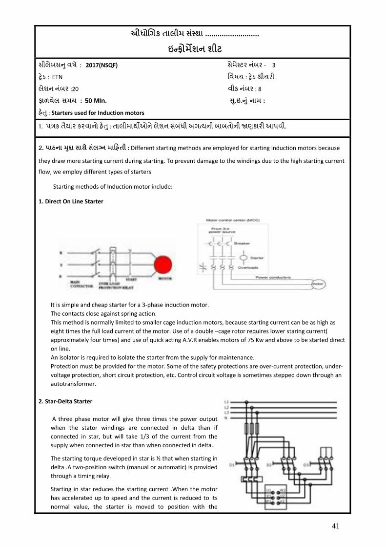
હતે ુ: Starters used for Induction motors
1. પત્રક તૈયાર કરવાનો હતે ુ: તાલીમાથીર્ઓને લેશન સબંધંી અગ યની બાબતોની જાણકારી આપવી.
2. પાઠના ુ ા સાથે સલં ન મા હતી : Different starting methods are employed for starting induction motors because
they draw more starting current during starting. To prevent damage to the windings due to the high starting current
flow, we employ different types of starters
Starting methods of Induction motor include:
1. Direct On Line Starter
It is simple and cheap starter for a 3‐phase induction motor.
The contacts close against spring action.
This method is normally limited to smaller cage induction motors, because starting current can be as high as
eight times the full load current of the motor. Use of a double –cage rotor requires lower staring current(
approximately four times) and use of quick acting A.V.R enables motors of 75 Kw and above to be started direct
on line.
An isolator is required to isolate the starter from the supply for maintenance.
Protection must be provided for the motor. Some of the safety protections are over‐current protection, under‐
voltage protection, short circuit protection, etc. Control circuit voltage is sometimes stepped down through an
autotransformer.
2. Star‐Delta Starter
A three phase motor will give three times the power output
when the stator windings are connected in delta than if
connected in star, but will take 1/3 of the current from the
supply when connected in star than when connected in delta.
The starting torque developed in star is ½ that when starting in
delta .A two‐position switch (manual or automatic) is provided
through a timing relay.
Starting in star reduces the starting current .When the motor
has accelerated up to speed and the current is reduced to its
normal value, the starter is moved to position with the

42
windings now connected in delta.
More complicated than the DOL starter, a motor with a star‐delta starter may not produce sufficient torque to
start against full load, so output is reduced in the start position. The motors are thus normally started under a
light load condition. Switching causes a transient current which may have peak values in excess of those with
DOL.
3. Auto Transformer Motor Starting
Operated by a two position switch i.e. manually / automatically using a timer to change over from start to run
position.
In starting position supply is connected to stator windings through an auto‐transformer which reduces applied
voltage to 50, 60, and 70% of normal value depending on tapping used.
Reduced voltage reduces current in motor windings with 50% tapping used motor current is halved and supply
current will be half of the motor current. Thus starting current taken from supply will only be 25% of the taken
by DOL starter.
For an induction motor, torque T is developed by V2, thus on 50% tapping, torque at starting is only (0.5V)2 of
the obtained by DOL starting. Hence 25% torque is produced.
Starters used in lager industries, it is larger in size and expensive.
Switching from start to run positions causing transient current, which can be greater in value than those
obtained by DOL starting.
4. Rotor Resistance Starter
This starter is used with a wound rotor induction motor. It uses an external resistance/phase in the rotor circuit
so that rotor will develop a high value of torque.
High torque is produced at low
speeds, when the external resistance
is at its higher value.
At start, supply power is connected
to stator through a three pole
contactor and, at a same time, an
external rotor resistance is added.
The high resistance limits staring
current and allows the motor to
start safely against high load.
Resistors are normally of the wire‐
wound type, connected through brushes and slip rings to each rotor phase. They are tapped with points
brought out to fixed contactors.
As the motor starts, the external rotor resistance is gradually cut out of circuit ; the handle or starter is turned
and moves the three contacts simultaneously from one fixed contact to the next.
The three moving contacts are interconnected to form a start point for the resistors.
To ensure that the motor cannot be started until all rotor resistance is in circuit, an interlock is fitted which
prevents the contactors from being closed until this condition is fulfilled.
43
ઔધોગક તાલીમ સં થા ..........................
ઇ ફોમશન શીટ
સીલેબસન ુવષૅ : 2017(NSQF) સેમે ટર નબંર ‐ 3
ટે્રડ : ETN િવષય : ટે્રડ થીયરી લેશન નબંર :21 વીક નબંર :9 ફાળવેલ સમય : 50 MIn. .ુઇ. ુ ંનામ :
હતે ુ: Cable signal diagram conventions.
1. પત્રક તૈયાર કરવાનો હતે ુ: તાલીમાથીર્ઓને લેશન સબંધંી અગ યની બાબતોની જાણકારી આપવી.
2. પાઠના ુ ા સાથે સલં ન મા હતી :
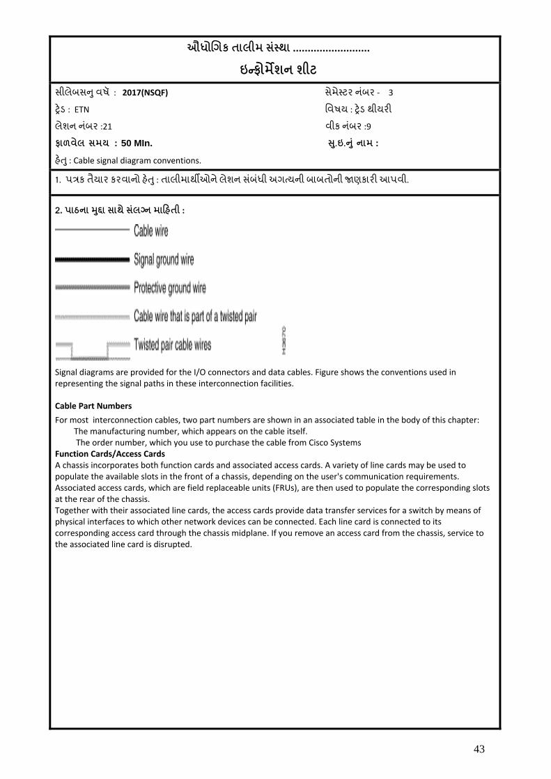
Signal diagrams are provided for the I/O connectors and data cables. Figure shows the conventions used in representing the signal paths in these interconnection facilities.
Cable Part Numbers
For most interconnection cables, two part numbers are shown in an associated table in the body of this chapter: The manufacturing number, which appears on the cable itself. The order number, which you use to purchase the cable from Cisco Systems Function Cards/Access Cards A chassis incorporates both function cards and associated access cards. A variety of line cards may be used to populate the available slots in the front of a chassis, depending on the user's communication requirements. Associated access cards, which are field replaceable units (FRUs), are then used to populate the corresponding slots at the rear of the chassis. Together with their associated line cards, the access cards provide data transfer services for a switch by means of physical interfaces to which other network devices can be connected. Each line card is connected to its corresponding access card through the chassis midplane. If you remove an access card from the chassis, service to the associated line card is disrupted.

44

45
ઔધોગક તાલીમ સં થા ..........................
ઇ ફોમશન શીટ
સીલેબસન ુવષૅ : 2017(NSQF) સેમે ટર નબંર ‐ 3
ટે્રડ : ETN િવષય : ટે્રડ થીયરી લેશન નબંર :22 વીક નબંર : 9 ફાળવેલ સમય : 50 MIn. .ુઇ. ુ ંનામ :
હતે ુ: Classification of electronic cables as per the application w.r.t. insulation, gauge, current capacity, flexibility etc.
1. પત્રક તૈયાર કરવાનો હતે ુ: તાલીમાથીર્ઓને લેશન સબંધંી અગ યની બાબતોની જાણકારી આપવી.
2. પાઠના ુ ા સાથે સલં ન મા હતી :
An electrical cable has different types, color and application as its determining factors. Non‐Metallic Sheathed Cable: These cables are also known as non‐metallic building wire or NM cables. They feature a flexible plastic jacket with two to four wires (TECK cables are covered with thermoplastic insulation) and a bare wire for grounding. Special varieties of this cable are used for underground or outdoor use, but NM‐B and NM‐C non‐metallic sheathed cables are the most common form of indoor residential cabling. Underground Feeder Cable: These cables are quite similar to NM cables, but instead of each wire being individually wrapped in thermoplastic, wires are grouped together and embedded in the flexible material. Available in a variety of gauge sizes, UF cables are often used for outdoor lighting and in‐ground applications. Their high water‐resistance makes them ideal for damp areas like gardens as well as open‐to‐air lamps, pumps, etc.
Metallic Sheathed Cable: Also known as armored or BX cables, metal‐sheathed cables are often used to supply mains electricity or for large appliances. They feature three plain stranded copper wires (one wire for the current, one grounding wire and one neutral wire) that are insulated with cross‐linked polyethylene, PVC bedding and a black PVC sheathing. BX cables with steel wire sheathing are often used for outdoor applications and high‐stress installations.
Multi‐Conductor Cable: This is a cable type that is commonly used in homes, since it is simple to use and well‐insulated. Multi‐conductor or multi‐core (MC) cables feature more than one conductor, each of which is insulated individually. In addition, an outer insulation layer is added for extra security. Different varieties are used in industries, like the audio multicore ‘snake cable’ used in the music industry.
Coaxial Cable: A coaxial cable features a tubular insulating layer that protects an inner conductor which is further surrounded by a tubular conducting shield, and might also feature an outer sheath for extra insulation. Called ‘coaxial’ since the two inner shields share the same geometric axis, these cables are normally used for carrying television signals and connecting video equipment.
Unshielded Twisted Pair Cable: Like the name suggests, this type consists of two wires that are twisted together. The individual wires are not insulated, which makes this cable perfect for signal transmission and video applications. Since they are more affordable than coaxial or optical fiber cables, UTP cables are often used in telephones, security cameras and data networks. For indoor use, UTP cables with copper wires or solid copper cores are a popular choice, since they are flexible and can be easily bent for in‐wall installation.
Ribbon Cable: Ribbon cables are often used in computers and peripherals, with various conducting wires that run parallel to each other on a flat plane, leading to a visual resemblance to flat ribbons. These cables are quite flexible and can only handle low voltage applications.
Direct‐Buried Cable: Also known as DBCs, these cables are specially‐designed coaxial or bundled fiber‐optic cables, which do not require any added sheathing, insulation or piping before being buried underground. They feature a heavy metal core with many layers of banded metal sheathing, heavy rubber coverings, shock‐absorbing gel and waterproof wrapped thread‐fortified tape. High tolerance to temperature changes, moisture and other environmental factors makes them a popular choice for transmission or communication requirements.

46
Twin‐Lead Cable: These are flat two‐wire cables that are used for transmission between an antenna and receiver, like TV and radio.
Twinaxial Cable: This is a variant of coaxial cables, which features two inner conductors instead of one and is used for very‐short‐range high‐speed signals.
Paired Cable: With two individually insulated conductors, this cable is normally used in DC or low‐frequency AC applications.
Twisted Pair: This cable is similar to paired cables, but the inner insulated wires are twisted or intertwined.

47
ઔધોગક તાલીમ સં થા ..........................
ઇ ફોમશન શીટ
સીલેબસન ુવષૅ : 2017(NSQF) સેમે ટર નબંર ‐ 3
ટે્રડ : ETN િવષય : ટે્રડ થીયરી લેશન નબંર :23 વીક નબંર : 10 ફાળવેલ સમય : 50 MIn. .ુઇ. ુ ંનામ :
હતે ુ: Different types of connectors .
1. પત્રક તૈયાર કરવાનો હતે ુ: તાલીમાથીર્ઓને લેશન સબંધંી અગ યની બાબતોની જાણકારી આપવી.
2. પાઠના ુ ા સાથે સલં ન મા હતી :
An electrical connector is an electro‐mechanical device for joining electrical circuits as an interface using a
mechanical assembly. Connectors consist of plugs (male‐ended) and jacks (female‐ended).
Types of electrical connectors Terminal blocks Terminal blocks provide a convenient means of connecting individual electrical wires without a splice or physically joining the ends. They are usually used to connect wiring among various items of equipment within an enclosure or to make connections among individually enclosed items. Posts A general type of connector that simply screws or clamps bare wire to a post; such connectors are frequently used in electronic test equipment and audio. Many, but not all binding posts will also accept a banana connector plug. Crimp‐on connectors A type of solder less connection. Insulation displacement connectors Insulation displacement connectors are usually used with small conductors for signal purposes and at low voltage. Power conductors carrying more than a few amperes are more reliably terminated with other means, though "hot tap" press‐on connectors find some use in automotive applications for additions to existing wiring. Plug and socket connectors Plug and socket connectors are usually made up of a male plug and a female receptacle Plugs generally have one or more pins or prongs that are inserted into openings in the mating socket. The connection between the mating metal parts must be sufficiently tight to make a good electrical connection and complete the circuit. Component and device connectors High‐power transistor switch module with large screw connectors and small crimped‐on "Fast‐on" connectors Electrical and electronic components and devices sometimes have plug and socket connectors or terminal blocks, but individual screw terminals and fast‐on or quick‐disconnect terminals are more common. Blade connector A blade connector is a type of single wire connection using a flat conductive blade which is inserted into a blade receptacle. Ring and spade terminals Ring style wire end blade connectors are normally sold in lots. The connectors in the top row of the image are known as ring terminals and spade terminals Electrical contact is made by the flat surface of the ring or spade, while mechanically they are attached by passing a screw or bolt through them. Commonly used connectors 8P8C connector 8P8C is short for "eight positions, eight conductors", and so an 8P8C modular connector (plug or jack) is a modular connector with eight positions, all containing conductors. The connector is probably most famous for its use in Ethernet and widely used on CAT5 cables. USB connectors The Universal Serial Bus is a serial bus standard to interface devices, founded in 1996. It is currently widely used among PCs, Apple Macintosh and many other devices. There are several types of USB connectors, and some have been added as the specification has progressed. The most commonly used is the (male) series "A" plug on peripherals, when the cable is fixed to the peripheral. If there is no cable fixed to the peripheral, the peripheral always needs to have a USB "B" socket. In this case a USB "A" plug to a USB "B" plug cable would be needed. USB "A" sockets are always used on the host PC and the USB "B" sockets on the peripherals. It is a 4‐pin connector,

48
surrounded by a shield. There are several other connectors in use, the mini‐A, mini‐ B and mini‐AB plug and socket.Power connectors A panel‐mounted IEC 60320 C14 male connector designed to accept AC line power Power connectors must protect people from accidental contact with energized conductors. Power connectors often include a safety ground connection as well as the power conductors. In larger sizes, these connectors must also safely contain any arc produced when an energized circuit is disconnected or may require interlocking to prevent opening a live circuit. Radio frequency connectors Connectors used at radio frequencies must not change the impedance of the transmission line of which they are part, otherwise signal reflection and losses will result. A radio‐frequency connector must not allow external signals into the circuit, and must prevent leakage of energy out of the circuit. At lower radio frequencies simple connectors can be used with success, but as the radio frequency increases, transmission line effects become more important, with small impedance variations from connectors causing the signal to reflect from the connector, rather than to pass through. At UHF and above, silver‐plating of connectors is common to reduce losses. Common types of RF connectors are used for television receivers, two‐way radio, certain Wi‐Fi devices with removable antennas, and industrial or scientific measuring instruments using radio frequencies. DC connectors A DC connector is an electrical connector for supplying direct current (DC) power. For portable consumer electronic devices, the coaxial power connector is frequently used, but many other types of connectors also exist. Hybrid connectors Hybrid connectors have housings with inserts that allow the intermixing of many connector types, such as those mentioned above. These housings may also allow intermixing of electrical and non‐electrical interfaces, examples of the latter being pneumatic line connectors, and optical fiber connectors. Because hybrid connectors are modular in nature, they tend to simplify assembly, repair, and future modifications. They also allow the creation of composite cable assemblies that can reduce equipment installation time by reducing the number of individual cable and connector assemblies. Banana Banana connectors are used to connect single wires to electrical equipment. They are often used with testing equipment. Barrier Strip/Spade Lug A connector that locks a metal spade to a terminal by screwing them together.. Crimp Crimp connectors can be used for fast and friction‐type connections in DC applications where connections are broken repeatedly. Alligator/Crocodile clip Alligator connectors are often used as temporary test leads. Screw terminal A screw terminal is a type of electrical connector where a wire is held by the tightening of a screw. Phone Phone connectors can be used as connectors in microphone cables and for low‐voltage, low‐current applications. RCA RCA connectors can be used in audio connections. DIN A DIN connector is suitable with multiple conductor wires for interconnecting audio and computer accessories. Tee A Tee connector is an electrical connector that connects three cables together.

49
ઔધોગક તાલીમ સં થા ..........................
ઇ ફોમશન શીટ સીલેબસ ુવષૅ : 2017(NSQF) સેમે ટર નબંર - 3 ડ : ETN િવષય : ડ થીયર
લેશન નબંર : 24 વીક નબંર :10 ફાળવેલ સમય : 50 MIn. .ુઇ. ુ ંનામ :
હ ુ: Different types of cable.
1. પ ક તૈયાર કરવાનો હ ુ: તાલીમાથીર્ઓને લેશન સબંધંી અગ યની બાબતોની જાણકારી આપવી.
2. પાઠના ુ ા સાથે સલં ન મા હતી : VGA Cable: Connect one end to: computer monitor, television Connect other end to: VGA port on computer DVI Cable: Connect one end to: computer monitor Connect other end to: DVI port on computer HDMI Cable Connect other end to: HDMI port on computer PS/2 Cable: Connect one end to: PS/2 keyboard, PS/2 mouse Connect other end to: PS/2 ports on computer Purple PS/2 port: keyboard Green PS/2 port: mouse Ethernet Cable: Connect one end to: router, network switch Connect other end to: Ethernet port on computer 3.5mm Audio Cable: Connect one end to: computer speakers, 3.5mm headphones, 3.5mm microphone connect other end to: audio ports on computer Green audio port: computer speakers or headphones Pink audio port: microphone Blue audio port: MP3 player, CD player, DVD player, turntable, electric guitar etc (line‐in port to play and record sounds from the above devices) USB Cable: Connect one end to: USB device Connect other end to: USB ports on computer How to tell USB 2.0 and 3.0 ports apart: USB 2.0 ports have black tips while USB 3.0 ports come with blue tips

50
51
ઔધોગક તાલીમ સં થા ..........................
ઇ ફોમશન શીટ
સીલેબસન ુવષૅ : 2017(NSQF) સેમે ટર નબંર ‐ 3 ટે્રડ : ETN િવષય : ટે્રડ થીયરી લેશન નબંર :25 વીક નબંર : 11 ફાળવેલ સમય : 50 MIn. .ુઇ. ુ ંનામ :
હતે ુ: : Principle and fading of Radio Wave Propagation.
1. પત્રક તૈયાર કરવાનો હતે ુ: તાલીમાથીર્ઓને લેશન સબંધંી અગ યની બાબતોની જાણકારી આપવી.
2. પાઠના ુ ા સાથે સલં ન મા હતી : Principle and fading of Radio Wave Radio propagation is the behavior of radio waves when they are transmitted, or propagated from one point on the Earth to another, or into various parts of the atmosphere. As a form of electromagnetic radiation, like light waves, radio waves are affected by the phenomena of reflection, refraction, diffraction, absorption, polarization, and scattering. Radio propagation is affected by the daily changes of water vapor in the troposphere and ionization in the upper atmosphere, due to the Sun. Understanding the effects of varying conditions on radio propagation has many practical applications, from choosing frequencies for international shortwave broadcasters, to designing reliable mobile telephone systems, to radio navigation, to operation of radar systems. Radio propagation is also affected by several other factors determined by its path from point to point. This path can be a direct line of sight path or an over‐the‐horizon path aided by refraction in the ionosphere, which is a region between approximately 60 and 600 km. In wireless communications, fading is deviation of the attenuation affecting a signal over certain propagation media. The fading may vary with time, geographical position or radio frequency, and is often modeled as a random process. A fading channel is a communication channel that experiences fading. In wireless systems, fading may either be due to multipath propagation, referred to as multipath induced fading, or due to shadowing from obstacles affecting the wave propagation, sometimes referred to as shadow fading. Slow fading arises when the coherence time of the channel is large relative to the delay constraint of the channel Fast fading occurs when the coherence time of the channel is small relative to the delay constraint of the channel. In this case, the amplitude and phase change imposed by the channel varies considerably over the period of use. Block fading is where the fading process is approximately constant for a number of symbol intervals. A channel can be 'doubly block‐fading' when it is block fading in both the time and frequency domains. Selective fading or frequency selective fading is a radio propagation anomaly caused by partial cancellation of a radio signal by itself — the signal arrives at the receiver by two different paths, and at least one of the paths is changing (lengthening or shortening). This typically happens in the early evening or early morning as the various layers in the ionosphere move, separate, and combine. The two paths can both be sky wave or one is ground wave. In flat fading, the coherence bandwidth of the channel is larger than the bandwidth of the signal. Therefore, all frequency components of the signal will experience the same magnitude of fading. In frequency‐selective fading, the coherence bandwidth of the channel is smaller than the bandwidth of the signal. Different frequency components of the signal therefore experience uncorrelated fading.

52

53
ઔધોગક તાલીમ સં થા ..........................
ઇ ફોમશન શીટ
સીલેબસન ુવષૅ : 2017(NSQF) સેમે ટર નબંર ‐ 3 ટે્રડ : ETN િવષય : ટે્રડ થીયરી લેશન નબંર : 26 વીક નબંર : 11 ફાળવેલ સમય : 50 MIn. .ુઇ. ુ ંનામ :
હતે ુ: Importance of Modulation and its types.
1. પત્રક તૈયાર કરવાનો હતે ુ: તાલીમાથીર્ઓને લેશન સબંધંી અગ યની બાબતોની જાણકારી આપવી.
2. પાઠના ુ ા સાથે સલં ન મા હતી : Importance of Modulation and its types. What is Modulation? The best way to define modulation is: The process of impressing low‐frequency information to be transmitted on to a high‐frequency wave, called the carrier wave, by changing the characteristics of its amplitude, frequency, or phase angle is called modulation. Another definition for modulation is: The process of altering the characteristics of the amplitude, frequency, or phase angle of the high‐frequency signal in accordance with the instantaneous value of the modulating wave is called modulation. Functions of the Carrier Wave The main function of the carrier wave is to carry the audio or video signal from the transmitter to the receiver. The wave that is resulted due to superimposition of audio signal and carrier wave is called the modulated wave. Need for Modulation The reason why low frequency signals cannot be transmitted over long distances through space is listed below: 1. Short Operating Range – When a wave has a large frequency, the energy associated with it will also be large. Thus low frequency signals have less power that does not enable them to travel over long distances. 2. Poor Radiation Efficiency – The radiation efficiency becomes very poor for low frequency signals. 3. Mutual Interference – If all audio frequencies are send continuously from different sources, they would all get mixed up and cause erroneous interference air. If modulation is done, each signal will occupy different frequency levels and can be transmitted simultaneously without any error. 4. Huge Antenna Requirement – For a effective signal transmission, the sending and receiving antenna should be at least 1/4th of the wave length of the signal. Thus, for small frequencies, the antenna will have kilometers of length. But if the signal has the range of Megahertz frequency, then the antenna size would be less. The carrier wave cannot be used alone for transmission purposes. Since its amplitude, frequency, and phase angle are constant with respect to some preference. Types of Modulation:
1) Amplitude Modulation 2) Frequency Modulation 3) Phase Modulation
.

54

55
ઔધોગક તાલીમ સં થા .......................... ઇ ફોમશન શીટ
સીલેબસન ુવષૅ : 2017(NSQF) સેમે ટર નબંર ‐ 3
ટે્રડ : ETN િવષય : ટે્રડ થીયરી લેશન નબંર : 27 વીક નબંર : 11 ફાળવેલ સમય : 50 MIn. .ુઇ. ુ ંનામ :
હતે ુ: Demodulation techniques.
1. પત્રક તૈયાર કરવાનો હતે ુ: તાલીમાથીર્ઓને લેશન સબંધંી અગ યની બાબતોની જાણકારી આપવી.
2. પાઠના ુ ા સાથે સલં ન મા હતી : Demodulation techniques. Demodulation is the act of extracting the original information‐bearing signal from a modulated carrier wave. A demodulator is an electronic circuit (or computer program in a software‐defined radio) that is used to recover the information content from the modulated carrier wave.[1] There are many types of modulation so there are many types of demodulators. The signal output from a demodulator may represent sound (an analog audio signal), images (an analog video signal) or binary data (a digital signal). Techniques There are several ways of demodulation depending on how parameters of the base‐band signal such as amplitude, frequency or phase are transmitted in the carrier signal. For example, for a signal modulated with a linear modulation like AM (amplitude modulation), we can use a synchronous detector. On the other hand, for a signal modulated with an angular modulation, we must use an FM (frequency modulation) demodulator or a PM (phase modulation) demodulator. AM radio An AM signal encodes the information onto the carrier wave by varying its amplitude in direct sympathy with the analogue signal to be sent. There are two methods used to demodulate AM signals: • The envelope detector is a very simple method of demodulation that does not require a coherent demodulator. It consists of an envelope detector that can be a rectifier (anything that will pass current in one direction only) or other non‐linear that enhances one half of the received signal over the other and a low‐pass filter. The rectifier may be in the form of a single diode or may be more complex. Many natural substances exhibit this rectification behavior, which is why it was the earliest modulation and demodulation technique used in radio. The filter is usually an RC low‐pass type but the filter function can sometimes be achieved by relying on the limited frequency response of the circuitry following the rectifier. The crystal set exploits the simplicity of AM modulation to produce a receiver with very few parts, using the crystal as the rectifier and the limited frequency response of the headphones as the filter. • The product detector multiplies the incoming signal by the signal of a local oscillator with the same frequency and phase as the carrier of the incoming signal. After filtering, the original audio signal will result. SSB is a form of AM in which the carrier is reduced or suppressed entirely, which require coherent demodulation. For further reading, see sideband. FM radio Frequency modulation (FM) has numerous advantages over AM such as better fidelity and noise immunity. However, it is much more complex to both modulate and demodulate a carrier wave with FM and AM predates it by several decades. There are several common types of FM demodulators: • The quadrature detector, which phase shifts the signal by 90 degrees and multiplies it with the unshifted version. One of the terms that drops out from this operation is the original information signal, which is selected and amplified. • The signal is fed into a PLL and the error signal is used as the demodulated signal. • The most common is a Foster‐Seeley discriminator. This is composed of an electronic filter which decreases the amplitude of some frequencies relative to others, followed by an AM demodulator. If the filter response changes linearly with frequency, the final analog output will be proportional to the input frequency, as desired. • A variant of the Foster‐Seeley discriminator called the ratio detector[2] • Another method uses two AM demodulators; one tuned to the high end of the band and the other to the low end, and feed the outputs into a difference amplifier. • Using a digital signal processor, as used in software‐defined radio.

56
57
ઔધોગક તાલીમ સં થા ..........................
ઇ ફોમશન શીટ
સીલેબસન ુવષૅ : 2017(NSQF) સેમે ટર નબંર ‐ 3
ટે્રડ : ETN િવષય : ટે્રડ થીયરી લેશન નબંર :28 વીક નબંર : 11 ફાળવેલ સમય : 50 MIn. .ુઇ. ુ ંનામ :
હતે ુ: Antenna, its types and application.
1. પત્રક તૈયાર કરવાનો હતે ુ: તાલીમાથીર્ઓને લેશન સબંધંી અગ યની બાબતોની જાણકારી આપવી.
2. પાઠના ુ ા સાથે સલં ન મા હતી : Antenna, its types and application: An antenna (plural antennae or antennas), or aerial, is an electrical device which converts electric power into radio waves, and vice versa. It is usually used with a radio transmitter or radio receiver. In transmission, a radio transmitter supplies an electric current oscillating at radio frequency (i.e. a high frequency alternating current (AC)) to the antenna's terminals, and the antenna radiates the energy from the current as electromagnetic waves (radio waves). In reception, an antenna intercepts some of the power of an electromagnetic wave in order to produce a tiny voltage at its terminals that is applied to a receiver to be amplified. Antenna types Isotropic: An isotropic antenna (isotropic radiator) is a hypothetical antenna that radiates equal signal power in all directions. It is a mathematical model that is used as the base of comparison to calculate the gain of real antennas. No real antenna can have an isotropic radiation pattern. However approximately isotropic antennas, constructed with multiple elements, are used in antenna testing. Monopole: Monopole antennas consist of a single radiating element such as a metal rod, often mounted over a conducting surface, a ground plane. One side of the feed line from the receiver or transmitter is connected to the rod, and the other side to the ground plane, which may be the Earth. Monopoles have an omnidirectional radiation pattern, so they are used for broad coverage of an area, and have vertical polarization. Dipole: The most widely‐used class of antenna, a dipole antenna consists of two symmetrical radiators such as metal rods or wires, with one side of the balanced feedline from the transmitter or receiver attached to each. A horizontal dipole radiates in two lobes perpendicular to the antenna's axis. A half‐wave dipole the most common type, has two collinear elements each a quarter wavelength long and a gain of 2.15 dBi. Used individually as low gain antennas, dipoles are also used as driven elements in many more complicated higher gain types of antennas. Array: Array antennas consist of multiple antennas working as a single antenna. Typically they consist of arrays of identical driven elements, usually dipoles fed in phase, giving increased gain over that of a single dipole. Loop:
Loop antennas consist of a loop or coil of wire. Loops with circumference of a wavelength or larger act similarly to
dipole antennas. However loops small in comparison to a wavelength act differently. They interact with the
magnetic field of the radio wave instead of the electric field as other antennas do, and so are relatively insensitive to
nearby electrical noise. However they have low radiation resistance, and so are inefficient for transmitting. They are
used as receiving antennas at low frequencies, and also as direction finding antennas.
Aperture
Aperture antennas are the main type of directional antennas used at microwave frequencies and above. They consist of a small dipole or loop feed antenna inside a three‐dimensional guiding structure large compared to a wavelength, with an aperture to emit the radio waves. Since the antenna structure itself is nonresonant they can be used over a wide frequency range by replacing or tuning the feed antenna. Traveling wave: Unlike the above antennas, traveling wave antennas are nonresonant so they have inherently broad bandwidth. They are typically wire antennas multiple wavelengths long, through which the voltage and current waves travel in one direction, instead of bouncing back and forth to form standing waves as in resonant antennas. They have linear polarization (except for the helical antenna). Unidirectional traveling wave antennas are terminated by a resistor at one end equal to the antenna's characteristic resistance, to absorb the waves from one direction. This makes them inefficient as transmitting antennas.

58

59
ઔધોગક તાલીમ સં થા ..........................
ઇ ફોમશન શીટ
સીલેબસન ુવષૅ : 2017(NSQF) સેમે ટર નબંર ‐ 3 ટે્રડ : ETN િવષય : ટે્રડ થીયરી લેશન નબંર : 29 વીક નબંર :12 ફાળવેલ સમય : 50 MIn. .ુઇ. ુ ંનામ :
હતે ુ: Introduction to AM,FM,PM,SSB‐SC,DSB‐SC
1. પત્રક તૈયાર કરવાનો હતે ુ: તાલીમાથીર્ઓને લેશન સબંધંી અગ યની બાબતોની જાણકારી આપવી.
2. પાઠના ુ ા સાથે સલં ન મા હતી : Introduction to AM,FM,PM,SSB‐SC,DSB‐SC: Amplitude Modulation (AM) The method of varying amplitude of a high frequency carrier wave in accordance with the information to be transmitted, keeping the frequency and phase of the carrier wave unchanged is called Amplitude Modulation. The information is considered as the modulating signal and it is superimposed on the carrier wave by applying both of them to the modulator. Frequency modulation (FM) In telecommunications and signal processing, frequency modulation (FM) is the encoding of information in a carrier wave by varying the instantaneous frequency of the wave. In analog signal applications, the difference between the instantaneous and the base frequency of the carrier is directly proportional to the instantaneous value of the input‐signal amplitude. Phase modulation (PM) Phase modulation (PM) is a modulation pattern that encodes information as variations in the instantaneous phase of a carrier wave. Phase modulation is widely used for transmitting radio waves and is an integral part of many digital transmission coding schemes that underlie a wide range of technologies like Wi‐Fi, GSM and satellite television. PM is used for signal and waveform generation in digital synthesizers, such as the Yamaha DX7 to implement FM synthesis. A related type of sound synthesis called phase distortion is used in the Casio CZ synthesizers. Single‐Sideband Suppressed‐Carrier (SSB‐SC): In radio communications, Single‐Sideband modulation (SSB) or Single‐Sideband Suppressed‐Carrier (SSB‐SC) is a refinement of amplitude modulation which uses transmitter power and bandwidth more efficiently. Amplitude modulation produces an output signal that has twice the bandwidth of the original baseband signal. Single‐sideband modulation avoids this bandwidth doubling, and the power wasted on a carrier, at the cost of increased device complexity and more difficult tuning at the receiver. Double‐sideband suppressed‐carrier transmission (DSB‐SC): Double‐sideband suppressed‐carrier transmission (DSB‐SC) is transmission in which frequencies produced by amplitude modulation (AM) are symmetrically spaced above and below the carrier frequency and the carrier level is reduced to the lowest practical level, ideally being completely suppressed. In the DSB‐SC modulation, unlike in AM, the wave carrier is not transmitted; thus, much of the power is distributed between the sidebands, which imply an increase of the cover in DSB‐SC, compared to AM, for the same power used. DSB‐SC transmission is a special case of double‐sideband reduced carrier transmission. It is used for radio data systems.

60

61
ઔધોિગક તાલીમ સં થા .......................... ઇ ફોમેર્શન શીટ
સીલેબસન ુવષૅ : 2017(NSQF) સેમે ટર નબંર ‐ 3 ટે્રડ : ETN િવષય : ટે્રડ થીયરી લેશન નબંર : 30 વીક નબંર : 12 ફાળવેલ સમય : 50 MIn. .ુઇ. ુ ંનામ :
હતે ુ: F M ા સમીટર લોક ડાયા ામ
1. પત્રક તૈયાર કરવાનો હતે ુ: તાલીમાથીર્ઓને લેશન સબંધંી અગ યની બાબતોની જાણકારી આપવી.
માઈ ોફોન : સાઉ ડિસગનલ ુઈલે કલ સી ન પ તરકર છે ટ મોડ લેુટર આપવામા ંઆવે છે
ર એ ટ સ મોડ લેુટર: ઓડ ઓ એ પાલી ુડપ રવતનનોને કવ સીપ રવતનોમા ંબદલે છે આ યા વગર કવ સી મો ુંલેસનકર શકાશે ન હ
હતેઓુ R F ઓસીલેટર : આ એક સામા ય િફ્રકવ સીઓસી લેટર 10MHZિફ્રકવ સી ઉ પન કરી શકે
િફ્રકવ સી મ ટી લાયર : આ ટેજમોડયલેુટેડ R.F.સીગ્નલની વો ટેજની સાથે કર ટ એટલે કે પાવર એ લીફીકેશન કરેછે.આ CLASS ‘C’ પ્રકારનુ ંહોય છે. નોરેિશયો 60 થી 75 સધુી નો હોય છે. સીગ્નલ ડીશટ્રોશન કરે છે.
A.F.C : આ ઓટોમેટીક િફકવ સી ક ટ્રોલનુ ંકાયર્ કરેછે. આપણે જાણીએ છીએ કે િફક્વે સી મોડયુલેંટેડ મા ંટ્રા સિમટરની િફકવ સી A.F િસગ્નલની અનશુારસનન પિરવિતર્ત થતી રહ ેછે. છેવટે પ્રશાિરત કરવાવાળી રેિડયો ફીક્ શીની વે ય ુિ થર રાખવામા ંઆવેછે. આકાયર્ને સપંન કરવા A.F.C ની જ ર પડે છે.
R.F ઓંશીલેટર : આ 9.9MHZ ની િફકવ સી પેદાકરે છે.
ફીક્વ સી મ ટીપલાયર : આ 9.9MHZ ની િફકવ સી દશગણી વધારીને 99MHZકરી નાખે છે.
િમક્સર : આ ટેજમા ં99MHZ અને 100MHZ વ ચે હીટ્રોડાઇઝીગ કરવામા ંઆવે છે. તેથી 1MHZ િફકવ સી મળે છે તે IF ટેજને આપવામા ંઆવે છે.
IF એ લીફાયર : આ 1MHZ ફીક્ સીનુ ંએ લીફીકે ન.
ડીસક્રીમીનેટેર : આ 1MHZ કાયર્ િ થર વે ય ુDC. ઓઉટ પટુ તેંયાર કરે છે.
આ DC OUT PUT વે ય ુિ થર રાખે છે.

62

63
ઔધોિગક તાલીમ સં થા .......................... ઇ ફોમેર્શન શીટ
સીલેબસન ુવષૅ : 2017(NSQF) સેમે ટર નબંર ‐ 3 ટે્રડ : ETN િવષય : ટે્રડ થીયરી લેશન નબંર : 31 વીક નબંર : 12 ફાળવેલ સમય : 50 MIn. .ુઇ. ુ ંનામ :
હતે ુ: FM જનરેશન અને ડીટેક્ષન
1. પત્રક તૈયાર કરવાનો હતે ુ: તાલીમાથીર્ઓને લેશન સબંધંી અગ યની બાબતોની જાણકારી આપવી.
2. પાઠના ુ ા સાથે સલં ન મા હતી :
આમ પ્ર યક્ષ FM ના િનમાર્ણ કેિરયરએ તેમેંસેજ િસગ્નલ ના પ્રમાણ મા ંબદલાયા કરે છે. તેના માટે VCO સાધન ઉપયોગ મા ંલેવાય છે.
સાયનો સીડયઅુલ ઓસીલેટર મા ંG ની િકમત વધ ુહોઈ યા ંVCO અમલ મા ંમકુાય છે.આ ઓસીલેતર ની િફ્રકવ સી આ સિકર્ટ ની અંદર રહલેા રીએક્ટીવ કા પોન મા ંથતા ફેરફારો બદલાય છે. જો સિકર્ટ મા ંL અને C એ મોડ લેુટ િસગ્નલ ના એ પલીટુડ સાથે બદલાય તો FM મજુબ બદલી શકાય .
FM િડટેકશન PLL ની મદદથી FM ન ુિડટેકશન ડીમોડ લેુટર અથવા FM િડટેકશન તરીકે PLL ઉપયોગી છે.
FM િસગ્નલ કે ને ડીમોડ લેુટર કરવાનુ ંછે તેને PLL ના ઈનપટુ સાથે આપવામા ંઆવે છે.
મ PLL એ FMિસગ લ સાથે લોક હોઈ છે. VCO એ FM ના ઈનપટુ િસગ લ ન ુટે્રકીંગ સરંુ કરે છે.
એ પલીફાયર ના આઉટપટુ મા ંએરર વો ટેજ પેદા થાય છે. FMસે ટર ફ્રીક્વનસી ની ઈનપટુ િફ્રકવ સી ના પ્રમાણ સર હોઈ છે.

64

65
ઔધોગક તાલીમ સં થા ..........................
ઇ ફોમશન શીટ
સીલેબસન ુવષૅ : 2017(NSQF) સેમે ટર નબંર ‐ 3
ટે્રડ : ETN િવષય : ટે્રડ થીયરી લેશન નબંર : 32 વીક નબંર :12 ફાળવેલ સમય : 50 MIn. .ુઇ. ુ ંનામ :
હતે ુ: Digital Modulation and Demodulation.
1. પત્રક તૈયાર કરવાનો હતે ુ: તાલીમાથીર્ઓને લેશન સબંધંી અગ યની બાબતોની જાણકારી આપવી.
2. પાઠના ુ ા સાથે સલં ન મા હતી : Digital Modulation and Demodulation:
Modulation Techniques: The figure below shows the modulation techniques that Communications System Toolbox™ supports for digital data. All the methods at the far right are implemented in library blocks.
Like analog modulation, digital modulation alters a transmittable signal according to the information in a message signal. However, in this case, the message signal is restricted to a finite set. Using this product, you can modulate or demodulate signals using various digital modulation techniques. You can also plot signal constellations. Modulation functions output the complex envelope of the modulated signal.
Accessing Digital Modulation Blocks. Open the Modulation library by double‐clicking the icon in the main block library. Then open the Digital Baseband sublibrary by double‐clicking its icon in the Modulation library.
Some digital modulation sublibraries contain blocks that implement special cases of a more general technique and are, in fact, special cases of a more general block. These special‐case blocks use the same computational code that their general counterparts use, but provide an interface that is either simpler or more suitable for the special case. The following table lists special‐case modulators, their general counterparts, and the conditions under which the two are equivalent. The situation is analogous for demodulators.

66

67
ઔધોગક તાલીમ સં થા .......................... ઇ ફોમશન શીટ
સીલેબસન ુવષૅ : 2017(NSQF) સેમે ટર નબંર ‐ 3 ટે્રડ : ETN િવષય : ટે્રડ થીયરી લેશન નબંર : 33 વીક નબંર :12 ફાળવેલ સમય : 50 MIn. .ુઇ. ુ ંનામ :
હતે ુ: AM,FM,PAM,PWM,PPM SIGNAL ુમ ટ લે ીગ તથા ડ મ ટ લે ીગ અ યાસ કરવા.
1. પત્રક તૈયાર કરવાનો હતે ુ: તાલીમાથીર્ઓને લેશન સબંધંી અગ યની બાબતોની જાણકારી આપવી.
મ ટ લે ર એટલે અનેક ઈન ટુ (એક કરતાવ ઈુન ટુ) માટ એકજ આઉટ ટુ વાળ સ કટ હોય છે, આ સ કટ મા ંક ોલ આપી આપણે ઈન ટુ અને આઉટ ટુ ા ત કર શકાય.
આ એક િસલે ટર વીચ પણ મ ટ લે ર ુકાય કર શક છે. MUX ની મદદથી ઘણી બધી જોડાણ વાળ સ કટ અમલમા ં કુાય છે.
ડ મ ટ લે ર અથ એ થાય છે ક એકમાથંી એક વધાર એક DUMUX મા ઈન ટુ પર ુ ંવ ુઆઉટ ટુ વાળ સ કટ હોય છે.
આ સ કટ મા ંકં ોલ સ કટ આપી ઈન ટુ મેળવી શકાય છે.
આ પ િત મા ંકર યર ફ વે સી તરંગો મા ંકોઈ ફરફાર થતો નથી, પરં ુતેના કદમા ઓડ યો િસ નલ ના માણ મા ફરફાર થાયછે.FM કરતા સા ુ અને સા ુ , સરળ અને સ ુ હોવાથી વધાર માણ મા ંવપરાય છે.
આ કાર ના મો ુ લેુશન ર ડયો ફ વ સી ક રયર વેવની ફકવ સી મા ંઓડ ઓ તરંગની ફ વે સી મા ં માણમા ંફરફાર થાય છે. ફ વે સી મો ું લેુશન હાઇફાયડા લીટ હોય છે. થી નોઈઝ વગર ુ ંઆઉટ ટુ મળે છે.
આ ડટા મોડ ુલેંશન ુસરળ પ છે. પીડ લસ ના કારણે એ પલીટ ડુ એ આવેલા મેસેઝ ની M (T )સે પલ ની કમત બદલાયા કર છે.
PAM વેવ ોમ ( લેટ ટોપેડ લસ હોય છે.દરક લસની એ પલીટ ડુએ લસની બ ડગ પરના મેસેજ િસ નલ X (T)ની ક મત થી બદલાયા કર છે.
આ પ ધિત છે મા ંર ટ ગ ુલંર પ સીસ એ એક જ કારના મળતા મેસેજ િસ નલ સાથે બદલાયા કર છે.
PAM ના બે કાર છે 1.ડબલ પોલારટ pam તેમા પોઝીટ વ અને નેગેટ વ બને પ સ આ િૃત જુબ હોય છે, cro પર મોડ ુલેંટડ જોવા મળે છે.
PPM પ સ પોઝીશન મોડયલેુશન મા બને પ સ એ લીટ ડુ અને પ સ ડુરેશન કો ટ ટ હશે, પરંત ુપ સની પોઝીશન એ મેંસેજ િસગનલ ના સે પલ વે ય ુના ડીજીટલ સી ગલ ના ટાઈમ એિક્ષસ પર ઈનકોડ કરશે. PPM ટેકનીક મા ંપ સ નો વધતો જતો સમય એ ચેનલ ની બે ડવીથ નકી કરશે CRO પર જોવા મળશે.

68
PWM ને પ સ ટાઈમ મોડયલેુશન અને પ સ લે થ મોડયલેુશન પણ કહ ેછે, PWM મેસેજ સી ગનલ દરેક પ સ ના સમય ગાળા ને બદલવા માટે ઉપયોગી છે,તેને પ સ ડયરેુશન મોડયલેુશન કહછેે. PWM ને પ સ ટાઈમ મોડયલેુશન અને પ સ લે થ મોડયલેુશન પણ કહ ેછે, PWM મેસેજ સી ગનલ દરેક પ સ ના સમય ગાળા ને બદલવા માટે ઉપયોગી છે,તેને પ સ ડયરેુશન મોડયલેુશન કહછેે.
wave forms

69
ઔધોગક તાલીમ સં થા ..........................
ઇ ફોમશન શીટ
સીલેબસન ુવષૅ : 2017(NSQF) સેમે ટર નબંર ‐ 3
ટે્રડ : ETN િવષય : ટે્રડ થીયરી લેશન નબંર : 34 વીક નબંર : 13 ફાળવેલ સમય : 50 MIn. .ુઇ. ુ ંનામ :
હતે ુ: Introduction to 8051 Microcontroller, architecture, pin details & bus system.
1. પત્રક તૈયાર કરવાનો હતે ુ: તાલીમાથીર્ઓને લેશન સબંધંી અગ યની બાબતોની જાણકારી આપવી.
2. પાઠના ુ ા સાથે સલં ન મા હતી : A microcontroller is an integrated circuit or a chip with a processor and other support devices like program memory, data memory, I/O ports, serial communication interface etc integrated together.
The general schematic diagram of 8051 microcontroller is shown above. We can see 3 system inputs, 3 control signals and 4 ports (for external interfacing). A Vcc power supply and ground is also shown. Now lets explain and go through each in detail. System inputs are necessary to make the micro controller functional. So the first and most important of this is power, marked as Vcc with a GND (ground potential). Without proper power supply, no electronic system would work. XTAL 1 and XTAL 2 are for the system clock inputs from crystal clock circuit. RESET input is required to initialize microcontroller to default/desired values and to make a new start. There are 3 control signals, EA, PSEN and ALE. These signals known as External Access (EA), Program Store Enable (PSEN), and Address Latch Enable (ALE) are used for external memory interfacing.
For describing pin diagram and pin configuration of 8051, we are taking into consideration a 40 pin DIP (Dual inline package). Now let’s go through pin configuration in detail. Pin‐40 : Named as Vcc is the main power source. Usually its +5V DC. You may note some pins are designated with two signals (shown in brackets). Pins 32‐39: Known as Port 0 (P0.0 to P0.7) – In addition to serving as I/O port, lower order address and data bus signals are multiplexed with this port (to serve the purpose of external memory interfacing). This is a bi directional I/O port (the only one in 8051) and external pull up resistors are required to function this port as I/O. Pin‐31:‐ ALE aka Address Latch Enable is used to demultiplex the address‐data signal of port 0 (for external memory interfacing.) 2 ALE pulses are available for each
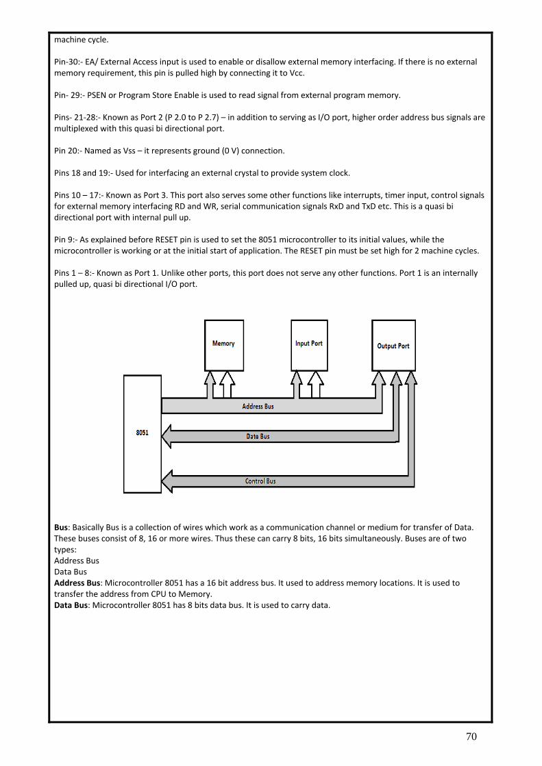
70
machine cycle. Pin‐30:‐ EA/ External Access input is used to enable or disallow external memory interfacing. If there is no external memory requirement, this pin is pulled high by connecting it to Vcc. Pin‐ 29:‐ PSEN or Program Store Enable is used to read signal from external program memory. Pins‐ 21‐28:‐ Known as Port 2 (P 2.0 to P 2.7) – in addition to serving as I/O port, higher order address bus signals are multiplexed with this quasi bi directional port. Pin 20:‐ Named as Vss – it represents ground (0 V) connection. Pins 18 and 19:‐ Used for interfacing an external crystal to provide system clock. Pins 10 – 17:‐ Known as Port 3. This port also serves some other functions like interrupts, timer input, control signals for external memory interfacing RD and WR, serial communication signals RxD and TxD etc. This is a quasi bi directional port with internal pull up. Pin 9:‐ As explained before RESET pin is used to set the 8051 microcontroller to its initial values, while the microcontroller is working or at the initial start of application. The RESET pin must be set high for 2 machine cycles. Pins 1 – 8:‐ Known as Port 1. Unlike other ports, this port does not serve any other functions. Port 1 is an internally pulled up, quasi bi directional I/O port.
Bus: Basically Bus is a collection of wires which work as a communication channel or medium for transfer of Data. These buses consist of 8, 16 or more wires. Thus these can carry 8 bits, 16 bits simultaneously. Buses are of two types: Address Bus Data Bus Address Bus: Microcontroller 8051 has a 16 bit address bus. It used to address memory locations. It is used to transfer the address from CPU to Memory. Data Bus: Microcontroller 8051 has 8 bits data bus. It is used to carry data.

71
ઔધોગક તાલીમ સં થા ..........................
ઇ ફોમશન શીટ
સીલેબસન ુવષૅ : 2017(NSQF) સેમે ટર નબંર ‐ 3
ટે્રડ : ETN િવષય : ટે્રડ થીયરી લેશન નબંર : 35 વીક નબંર : 13 ફાળવેલ સમય : 50 MIn. .ુઇ. ુ ંનામ :
હતે ુ: Differentiate microcontroller with microprocessor.
1. પત્રક તૈયાર કરવાનો હતે ુ: તાલીમાથીર્ઓને લેશન સબંધંી અગ યની બાબતોની જાણકારી આપવી.
2. પાઠના ુ ા સાથે સલં ન મા હતી : Microprocessor Microprocessor is heart of Computer system It is just a processor. Memory and I/O components have to be connected externally Since memory and I/O has to be connected externally, the circuit becomes large. Cannot be used in compact systems and hence inefficient Cost of the entire system increases Due to external components, the entire power consumption is high. Hence it is not suitable to used with devices running on stored power like batteries. Most of the microprocessors do not have power saving features. Since memory and I/O components are all external, each instruction will need external operation, hence it is relatively slower. Microprocessor have less number of registers, hence more operations are memory based. Microprocessors are based on von Neumann model/architecture where program and data are stored in same memory moduleMainly used in personal computers Micro Controller Micro Controller is a heart of embedded system Micro controller has external processor along with internal memory and i/O components Since memory and I/O are present internally, the circuit is small Can be used in compact systems and hence it is an efficient technique Cost of the entire system is low Since external components are low, total power Consumption is less and can be used with devices running on stored power like batteries. Most of the micro controllers have power saving modes like idle mode and power saving mode. This helps to reduce power consumption even further. Since components are internal, most of the operations are internal instruction, hence speed is fast Micro controller have more number of registers, hence the programs are easier to write Micro controllers are based on Harvard architecture where program memory and Data memory are separate Used mainly in washing machine, MP3 players

72

73
ઔધોગક તાલીમ સં થા ..........................
ઇ ફોમશન શીટ
સીલેબસન ુવષૅ : 2017(NSQF) સેમે ટર નબંર ‐ 3 ટે્રડ : ETN િવષય : ટે્રડ થીયરી લેશન નબંર : 36 વીક નબંર : 13 ફાળવેલ સમય : 50 MIn. .ુઇ. ુ ંનામ :
હતે ુ: Interfacing of memory to the microcontroller its I/O port pin configuration, Register banks,SFRs.
1. પત્રક તૈયાર કરવાનો હતે ુ: તાલીમાથીર્ઓને લેશન સબંધંી અગ યની બાબતોની જાણકારી આપવી.
2. પાઠના ુ ા સાથે સલં ન મા હતી : The microcontroller has two types of memory and these are Program Memory and Data Memory. Program Memory (ROM) is used to permanently save the program being executed, while Data Memory (RAM) is used for temporarily storing data and intermediate results created and used during the operation of the microcontroller. Program Memory Even though such an amount of memory is sufficient for writing most of the programs, there are situations when it is necessary to use additional memory as well. A typical example is so called lookup tables. They are used in cases when equations describing some processes are too complicated or when there is no time for solving them. In such cases all necessary estimates and approximates are executed in advance and the final results are put in the tables EA=0 In this case, the microcontroller completely ignores internal program memory and executes only the program stored in external memory. EA=1 In this case, the microcontroller executes first the program from built‐in ROM, and then the program stored in external memory. Data Memory As already mentioned, Data Memory is used for temporarily storing data and intermediate results created and used during the operation of the microcontroller. Besides, RAM memory built in the 8051 family includes many registers such as hardware counters and timers, input/output ports, serial data buffers etc. All 8051 microcontrollers have 4 I/O ports each comprising 8 bits which can be configured as inputs or outputs. Accordingly, in total of 32 input/output pins enabling the microcontroller to be connected to peripheral devices are available for use. Pin configuration, i.e. whether it is to be configured as an input (1) or an output (0), depends on its logic state. In order to configure a microcontroller pin as an output, it is necessary to apply logic zero (0) to appropriate I/O port bit. In this case, voltage level on appropriate pin will be 0. Port 0 The P0 port is characterized by two functions. If external memory is used then the lower address byte (addresses A0‐A7) is applied on it. Otherwise, all bits of this port are configured as inputs/outputs. The other function is expressed when it is configured as an output. Unlike other ports consisting of pins with built‐in pull‐up resistor connected by its end to 5 V power supply, pins of this port have this resistor left out. This apparently small difference has its consequences: Port 1 P1 is a true I/O port, because it doesn't have any alternative functions as is the case with P0, but can be configured as general I/O only. It has a pull‐up resistor built‐in and is completely compatible with TTL circuits. Port 2 P2 acts similarly to P0 when external memory is used. Pins of this port occupy addresses intended for external memory chip. This time it is about the higher address byte with addresses A8‐A15. When no memory is added, this port can be used as a general input/output port showing features similar to P1. Port 3 All port pins can be used as general I/O, but they also have an alternative function. In order to use these alternative functions, a logic one (1) must be applied to appropriate bit of the P3 register. In tems of hardware, this port is

74
similar to P0, with the difference that its pins have a pull‐up resistor built‐in.The 8051 microcontroller contains mainly two types of registers: General purpose registers (Byte addressable registers) Special function registers (Bit addressable registers) The 8051 microcontroller consists of 256 bytes of RAM memory, which is divided into two ways, such as 128 bytes for general purpose and 128 bytes for special function registers (SFR) memory. The memory which is used for general purpose is called as RAM memory, and the memory used for SFR contains all the peripheral related registers like Accumulator, ‘B’ register, Timers or Counters, and interrupt related registers.
General Purpose Registers
The general purpose memory is called as the RAM memory of the 8051 microcontroller, which is divided into 3 areas such as banks, bit‐addressable area, and scratch‐pad area. The banks contain different general purpose registers such as R0‐R7, and all such registers are byte‐addressable registers that store or remove only 1‐byte of data. Banks and Registers The B0, B1, B2, and B3 stand for banks and each bank contains eight general purpose registers ranging from ‘R0’ to ‘R7’. All these registers are byte‐addressable registers. Data transfer between general purpose registers to general purpose registers is not possible. These banks are selected by the Program Status Word (PSW) register. PSW (Program Status Word) Register The PSW register is a bit and byte‐addressable register. This register reflects the status of the operation that is carried out in the controller. Special Function Registers (SFR) Special function registers are upper RAM memory in the 8051 microcontroller. These registers contain all peripheral related registers like P0, P1, P2, P3, timers or counters, serial port and interrupts‐related registers. The SFR memory address starts from 80h to FFh. The SFR register is implemented by bit‐address registers and byte‐address registers. The accumulator, B register, Po, P1, P2, P3, IE registers are bit‐addressable register remaining all are byte‐addressable registers. Accumulator The accumulator which is also known as ACC or A is a bit as well as a byte‐addressable register by an address of the accumulator. If you want to use a bit‐addressable register, you can use a single bit (E0) of register and you can use an 8‐bit of the accumulator as a byte‐addressable register. The accumulator holds the results of most Arithmetic and logical operations. B‐Register The B‐register is a bit and byte‐addressable register. You can access 1‐bit or all 8‐bits by a physical address F0h. Suppose to access a bit 1, we have to use f1. The B register is only used for multiplication and division operations.

75
ઔધોગક તાલીમ સં થા ..........................
ઇ ફોમશન શીટ
સીલેબસન ુવષૅ : 2017(NSQF) સેમે ટર નબંર ‐ 3
ટે્રડ : ETN િવષય : ટે્રડ થીયરી લેશન નબંર : 37 વીક નબંર : 14 ફાળવેલ સમય : 50 MIn. .ુઇ. ુ ંનામ :
હતે ુ: Application of microcontroller in domestic, consumer & industries.
1. પત્રક તૈયાર કરવાનો હતે ુ: તાલીમાથીર્ઓને લેશન સબંધંી અગ યની બાબતોની જાણકારી આપવી.
2. પાઠના ુ ા સાથે સલં ન મા હતી : Domestic Application Refrigeration — Power efficiency is key for refrigeration equipment. Microcontrollers provide flexible connectivity options and power efficient architectures that are an excellent fit for refrigeration applications. Cooking — Cooking appliances such as stoves, microwave ovens, and conventional ovens, often require a combination of temperature and mass sensors, programmable timers, and sophisticated motor control for fan and other devices. Some include remote controls, and rich, responsive touch control interfaces are key for ease of use. Microcontrollers are ideal for cooking appliances. Washing — Washing machines require support for motor controls, water level and temperature sensing, and user interface components that can withstand harsh environments. Standards‐based, secure connectivity is also a must for appliances that will connect to a home network. A rich array of microcontrollers and touch screen solutions that can power today's advanced washing equipment. Motor Control — Microcontrollers are more and more common in motor control applications and are replacing Application‐Specific Standard Products (ASSP) and ASICs. Consumer Application For Digital A/V The DVD recorder can record digital HiDef TV programs, and play optical disks such as DVD‐R/RW. When the recorder is connected with an HDMI cable to other equipment the recorder’s on/off power supply and display can be controlled by a single remote control. Microcontrollers make these functionalities possible. For Digital Cameras Digital cameras convert images into electric signals using a semiconductor device reacts to light. The camera records electric signals as digital data in storage media, such as flash memory. Microcontroller family includes products that are well‐suited for this application. For LED Light Bulbs LED light bulbs are a common replacement for incandescent lamps because LEDs have longer life spans and are more power efficient, benefits that can be enhanced with dimmers. Microcontroller and LED drivers can control LED illumination and save power. For Printers and Faxes (MFP) Multifunction monochrome/color printers and faxes keep getting faster and more sophisticated to meet the needs of a 24/7 economy. As this equipment evolves, high‐resolution image processors and faster control of the document feeder are required. Microcontrollers achieve the high‐speed, precise motor control the printer’s engine requires. Industrial Applications: For Inverters: A major benefit of using an inverter for motor speed control is the energy savings. Inverters can accurately control motors over a wide speed range and keep the motor from stopping and restarting, which drains energy. The microcontroller is key to controlling the inverter. For Metering Systems Meters are used in lifeline applications such as power, gas and water systems. The industry is moving from conventional mechanical meters to smart meters with wired/wireless communication functions for automated data transfer. Smart meters with real‐time data logging are required for highly reliable systems and low power consumption. Microcontrollers facilitate development of meter systems, as well as reduce their BOM and other costs, helping to make the end product highly competitive. For PLC: The functionality of the PLC has evolved over the years to include sequential relay control, motion control, process control, distributed control systems, networking and security. The Spansion MCUs for PLC control help make these features possible.

76

77
ઔધોગક તાલીમ સં થા ..........................
ઇ ફોમશન શીટ
સીલેબસન ુવષૅ : 2017(NSQF) સેમે ટર નબંર ‐ 3
ટે્રડ : ETN િવષય : ટે્રડ થીયરી લેશન નબંર : 38 વીક નબંર : 14 ફા ફાળવેલ સમય : 50 MIn. .ુઇ. ુ ંનામ :
હતે ુ: Difference between 8051 & 8052.
1. પત્રક તૈયાર કરવાનો હતે ુ: તાલીમાથીર્ઓને લેશન સબંધંી અગ યની બાબતોની જાણકારી આપવી.
2. પાઠના ુ ા સાથે સલં ન મા હતી : Difference between 8051 & 8052. The 8052 is a super‐set of the original 8051. It added 128 more bytes of internal RAM and another 16‐bit timer, for a total of three counters. Clocks per instruction cycle for 8051 & 8052 is 12 Timers for 8051 & 8052 is 2 & 3 UARTs/serial ports for 8051 & 8052 is 1 Internal DATA RAM bytes for 8051 & 8052 is 128 & 256 Maximum program size without external logic for 8051 & 8052 is 64K Maximum PIO port pins for 8051 & 8052 is 32 Number of interrupts pins for 8051 & 8052 is Fixed

78

79
ઔધોગક તાલીમ સં થા .......................... ઇ ફોમશન શીટ
સીલેબસન ુવષૅ : 2017(NSQF) સેમે ટર નબંર ‐ 3 ટે્રડ : ETN િવષય : ટે્રડ થીયરી લેશન નબંર :39 વીક નબંર : 14 ફાળવેલ સમય : 50 MIn. .ુઇ. ુ ંનામ :
હતે ુ: Introduction to PIC Architecture
1. પત્રક તૈયાર કરવાનો હતે ુ: તાલીમાથીર્ઓને લેશન સબંધંી અગ યની બાબતોની જાણકારી આપવી.
2. પાઠના ુ ા સાથે સલં ન મા હતી : PIC is a Peripheral Interface Microcontroller which was developed in the year 1993 by the General Instruments Microcontrollers. It is controlled by software and programmed in such a way that it performs different tasks and controls a generation line. PIC microcontrollers are used in different new applications such as smart phones, audio accessories and advanced medical devices.
PIC Microcontrollers Architecture
The PIC microcontroller is based on RISC architecture. Its memory architecture follows the Harvard pattern of separate memories for program and data, with separate buses.
1. Memory Structure
The PIC architecture consists of two memories: Program memory and the Data memory. Program Memory: This is a 4K*14 memory space. It is used to store 13‐bit instructions, or the program code. The program memory data is accessed by the program counter register that holds the address of the program memory. The address 0000H is used as reset memory space and 0004H is used as interrupt memory space. Data Memory: The data memory consists of the 368 bytes of RAM and 256 bytes of EEPROM. The 368 bytes of RAM consists of multiple banks. Each bank consists of general purpose registers and special function registers. The special function registers consists of control registers to control different operations of the chip resources like Timers, Analog to Digital Converters, Serial ports, I/O ports, etc. For example, the TRISA register whose bits can be changed to alter the input or output operations of the port A. The general purpose registers consists of registers that are used to store temporary data and processing results of the data. These general purpose registers are each 8‐bit registers. Working Register: It consists of a memory space that stores the operands for each instruction. It also stores the results of each execution. Status Register: The bits of the status register denote the status of the ALU (arithmetic logic unit) after every execution of the instruction. It is also used to select any one of the 4 banks of the RAM. File Selection Register: It acts as a pointer to any other general‐purpose register. It consists of a register file address, and it is used in indirect addressing. Another general purpose register is the program‐counter register, which is a 13‐bit register. The 5 upper bits are used as PCLATH (Program Counter Latch) to independently function as any other register, and the lower 8‐bits are used as the program counter bits. The program counter acts as a pointer to the instructions stored in the program memory. EEPROM: It consists of 256 bytes of memory space. It is a permanent memory like ROM, but its contents can be erased and changed during the operation of the microcontroller. The contents into EEPROM can be read from or written to, using special function registers like EECON1, EECON2, EEDATA, etc.
2. I/O Ports
PIC16 series consists of five ports, such as Port A, Port B, Port C, Port D and Port E. Port A: It is a 16‐bit port, which can be used as input or output port based on the status of the TRISA register. Port B: It is an 8‐bit port, which can be used as both input and output port. 4 of its bits when used as input can be changed upon interrupt signals. Port C: It is an 8‐bit port whose operation (input or output) is determined by the status of the TRISC register. Port D: It is an 8‐bit port, which apart from being an I/O port, acts as a slave port for connection to the microprocessor bus. Port E: It is a 3‐bit port that serves the additional function of the control signals to the A/D converter.

80
3. Timers
PIC microcontrollers consist of 3 timers, out of which the Timer 0 and Timer 2 are 8‐bit timers and the Time‐1 is a 16‐bit timer, which can also be used as a counter.
4. A/D Converter
The PIC Microcontroller consists of 8‐channels, 10‐bit Analog to Digital Converter. The operation of the A/D converter is controlled by these special function registers: ADCON0 and ADCON1. The lower bits of the converter are stored in ADRESL (8 bits), and the upper bits are stored in the ADRESH register. It requires an analog reference voltage of 5V for its operation.
5. Oscillators
Oscillators are used for timing generation. PIC microcontrollers consist of external oscillators like crystals or RC oscillators. In case of crystal oscillators, the crystal is connected between two oscillator pins, and the value of the capacitor connected to each pin determines the mode of operation of the oscillator. The different modes are low‐power mode, crystal mode and the high‐ speed mode. In case of RC oscillators, the value of the Resistor and Capacitor determine the clock frequency. The clock frequency ranges from 30 KHz to 4 MHz.
6. CCP module:
A CCP module works in the following three modes: Capture Mode: This mode captures the time of arrival of a signal, or in other words, captures the value of the Timer1 when the CCP pin goes high. Compare Mode: It acts as an analog comparator that generates an output when the timer1 value reaches a certain reference value. PWM Mode: It provides pulse width modulated output with a 10‐bit resolution and programmable duty cycle. Other special peripherals include a Watchdog timer that resets the microcontroller in case of any software malfunction and a Brown out reset that resets the microcontroller in case of any power fluctuation and others. For better understanding of this PIC microcontroller we are giving one practical project which uses this controller for its operation.

81
ઔધોગક તાલીમ સં થા ..........................
ઇ ફોમશન શીટ
સીલેબસન ુવષૅ : 2017(NSQF) સેમે ટર નબંર ‐ 3
ટે્રડ : ETN િવષય : ટે્રડ થીયરી લેશન નબંર : 40 વીક નબંર : 15 ફાળવેલ સમય : 50 MIn. .ુઇ. ુ ંનામ :
હતે ુ: Basics of Transducers.
1. પત્રક તૈયાર કરવાનો હતે ુ: તાલીમાથીર્ઓને લેશન સબંધંી અગ યની બાબતોની જાણકારી આપવી.
2. પાઠના ુ ા સાથે સલં ન મા હતી : A transducer is a device that converts one form of energy to another form of energy. Energy types include electrical, mechanical, electromagnetic (including light), chemical, acoustic, and thermal energy. Usually a transducer converts a signal in one form of energy to a signal in another. There are two types of transducer 1 Active transducer 2 Passive transducer A transducer will have basically two main components. They are 1. Sensing Element The physical quantity or its rate of change is sensed and responded to by this part of the transistor. 2. Transduction Element The output of the sensing element is passed on to the transduction element. This element is responsible for converting the non‐electrical signal into its proportional electrical signal. Selection of Transducer Selection depends on the physical quantity to be measured. Depends on the best transducer principle for the given physical input. Depends on the order of accuracy to be obtained. Transducer Classification Based on their application. Based on the method of converting the non‐electric signal into electric signal. Based on the output electrical quantity to be produced. Based on the electrical phenomenon or parameter that may be changed due to the whole process. Based on whether the transducer is active or passive. Transducer Applications The applications of transducers based on the electric parameter used and the principle involved is given below. The applications of transducers based on the electric parameter used and the principle involved is given below. 1. Passive Type Transducers
a. Resistance Variation Type Resistance Strain Gauge Resistance Thermometer Resistance Hygrometer Hot Wire Meter

82
Photoconductive Cell Thermistor Potentiometer Type b. Capacitance Variation Type Variable Capacitance Pressure Gauge Dielectric Gauge Capacitor Microphone c. Inductance Variation Type Eddy Current Transducer Variable Reluctance Type Proximity Inductance Type Differential Transformer Magnetostrictive Transducer d. Voltage and Current Type Photo‐emissive Cell Hall Effect Ionisation Chamber
2. Active Type Photo‐voltaic Cell Thermopile Piezoelectric Type Moving Coil Type

83
ઔધોગક તાલીમ સં થા ..........................
ઇ ફોમશન શીટ
સીલેબસન ુવષૅ : 2017(NSQF) સેમે ટર નબંર ‐ 3 ટે્રડ : ETN િવષય : ટે્રડ થીયરી લેશન નબંર : 41 વીક નબંર : 15 ફાળવેલ સમય : 50 MIn. .ુઇ. ુ ંનામ :
હતે ુ: Working principle of RTD,PT‐100,Thermocouple,Sensor voltage and current formats.
1. પત્રક તૈયાર કરવાનો હતે ુ: તાલીમાથીર્ઓને લેશન સબંધંી અગ યની બાબતોની જાણકારી આપવી.
2. પાઠના ુ ા સાથે સલં ન મા હતી : An RTD (resistance temperature detector) is a temperature sensor that operates on the measurement principle that a material’s electrical resistance changes with temperature. The relationship between an RTD’s resistance and the surrounding temperature is highly predictable, allowing for accurate and consistent temperature measurement. By supplying an RTD with a constant current and measuring the resulting voltage drop across the resistor, the RTD’s resistance can be calculated, and the temperature can be determined. Pt‐100 or pt100 is one of the most used temperature sensor. It is one of the most used temperature sensor.
Pt‐100 temperature naming and working principle:
Pt‐100 is named as such because platinum is used as the sensing material and at with perfect calibration it has 100 ohm resistance at 0°c. For increment or decrement of temperature, the resistance value of platinum changes linearly.Thus it can be used to identify the temperature by comparing the resistance value and temperature‐resistance variation log value (provide by manufacturer). The zero scale for pt‐100 is 100 ohm at 0°c. Thus the measuring value of pt‐100 is resistance and for thermocouple temperature sensor measuring parameter is voltage. With the measuring value matching by chart the perspective temperature can be found. In PLC programming for a certain pt‐100, the temperature log chart with resistance is programmed, thus it can be used in automation system A thermocouple is a device used extensively for measuring temperature. Working Principle The working principle of thermocouple is based on three effects, discovered by Seebeck, Peltier and Thomson. They are as follows: 1) Seebeck effect: The Seebeck effect states that when two different or unlike metals are joined together at two junctions, an electromotive force (emf) is generated at the two junctions. The amount of emf generated is different for different combinations of the metals. 2) Peltier effect: As per the Peltier effect, when two dissimilar metals are joined together to form two junctions, emf is generated within the circuit due to the different temperatures of the two junctions of the circuit. 3) Thomson effect: As per the Thomson effect, when two unlike metals are joined together forming two junctions, the potential exists within the circuit due to temperature gradient along the entire length of the conductors within the circuit

84
85
ઔધોગક તાલીમ સં થા ..........................
ઇ ફોમશન શીટ
સીલેબસન ુવષૅ : 2017(NSQF) સેમે ટર નબંર ‐ 3
ટે્રડ : ETN િવષય : ટે્રડ થીયરી લેશન નબંર : 42 વીક નબંર : 16 ફાળવેલ સમય : 50 MIn. .ુઇ. ુ ંનામ :
હતે ુ: Basics of Thermistors,Thermocouples,Strain gauges,Load cell, Capacitive transducer, Inductive
transducers,LVDT,Proximity sensors.
1. પત્રક તૈયાર કરવાનો હતે ુ: તાલીમાથીર્ઓને લેશન સબંધંી અગ યની બાબતોની જાણકારી આપવી.
2. પાઠના ુ ા સાથે સલં ન મા હતી : What is a thermistor? A thermistor is a resistance thermometer, or a resistor whose resistance is dependent on temperature. It is made of metallic oxides, pressed into a bead, disk, or cylindrical shape and then encapsulated with an impermeable material such as epoxy or glass. There are two types of thermistors: Negative Temperature Coefficient (NTC) and Positive Temperature Coefficient (PTC). With an NTC thermistor, when the temperature increases, resistance decreases. Conversely, when temperature decreases, resistance increases. This type of thermistor is used the most. A PTC thermistor works a little differently. When temperature increases, the resistance increases, and when temperature decreases, resistance decreases. This type of thermistor is generally used as a fuse. What is a Thermocouple? A thermocouple is a device used extensively for measuring temperature. Learn how the device works here. A thermocouple is comprised of at least two metals joined together to form two junctions. One is connected to the body whose temperature is to be measured; this is the hot or measuring junction. The other junction is connected to a body of known temperature; this is the cold or reference junction. Therefore the thermocouple measures unknown temperature of the body with reference to the known temperature of the other body. What is a strain gage? A strain gage, a device whose electrical resistance varies in proportion to the amount of strain in the device. The most widely used gage is the bonded metallic strain gage. The metallic strain gage consists of a very fine wire or metallic foil arranged in a grid pattern. The grid pattern maximizes the amount of metallic wire or foil subject to strain in the parallel direction The cross‐sectional area of the grid is minimized to reduce the effect of shear strain and Poisson Strain. The grid is bonded to a thin backing, called the carrier, which is attached directly to the test specimen. Therefore, the strain experienced by the test specimen is transferred directly to the strain gage, which responds with a linear change in electrical resistance. Strain gages are available commercially with nominal resistance values from 30 to 3,000 Ω, with 120, 350, and 1,000 Ω being the most common values. What is a load cell? A load cell is a sensor or a transducer that converts a load or force acting on it into an electronic signal. This electronic signal can be a voltage change, current change or frequency change depending on the type of load cell and circuitry used. Load cells or Load sensors as they are commonly called ‐ can be made using resistive, capacitive, inductive or other techniques. Most commonly available load cells are based on the principle of change of resistance in response to an applied load. This is termed piezo‐resistive i.e. something that changes in response to an applied pressure (or squeezed). Loadstar Sensors has pioneered the use of capacitive techniques to build rugged, small digital load cells with high level USB, Wi‐Fi, XBee Wireless and Bluetooth outputs.

86
What is a Capacitive transducer? The capacitive transducer is nothing but the capacitor with variable capacitance. PRINCIPLE: The capacitance of the capacitor varies as the material comes between two plates of capacitor and the presence of something is measured by capacitance. OPERATION: When voltage is applied to the conductive objects the charges get collected on each object. The moving charges causes alternating current in the space between them and current flowing measured as capacitance. ADVANTAGES: Construction is simple. Cost of transducer is low. It has very high sensitivity. What is Inductive transducer? The inductive transducers work on the principle of the magnetic induction of magnetic material. Just as the resistance of the electric conductor depends on number of factors, the induction of the magnetic material depends on a number of variables like the number of turns of the coil on the material, the size of the magnetic material, and the permeability of the flux path. In the inductive transducers the magnetic materials are used in the flux path and there are one or more air gaps. The change in the air gap also results in change in the inductance of the circuit and in most of the inductive transducers it is used for the working of the instrument. What is a LVDT? The LVDT is an acronym used for Linear Variable Differential Transformer. It is a Transformer which is used for measuring linear displacement. When we gives supply to the primary winding of the LVDT, a current starts flowing through the primary winding. Due to magnetic property of current, the magnetic lines of force starts flowing around the primary coil, thus a magnetic field is set up around the primary winding. As in general transformers, due to magnetic effect of primary winding, an e.m.f. is also set up in secondary winding when the magnetic lines of force of primary winding cuts (come across contact) the iron rod and secondary winding. This e.m.f. causes a current to flow in secondary winding and this whole process is known as mutual inductance. What is a Proximity sensor? A proximity sensor is a sensor able to detect the presence of nearby objects without any physical contact. A proximity sensor often emits an electromagnetic field or a beam of electromagnetic radiation, and looks for changes in the field or return signal. The object being sensed is often referred to as the proximity sensor's target. Different proximity sensor targets demand different sensors. The maximum distance that this sensor can detect is defined "nominal range". Some sensors have adjustments of the nominal range or means to report a graduated detection distance. Proximity sensors can have a high reliability and long functional life because of the absence of mechanical parts and lack of physical contact between sensor and the sensed object.

87
ઔધોગક તાલીમ સં થા ..........................
ઇ ફોમશન શીટ સીલેબસ ુવષૅ : 2017(NSQF) સેમે ટર નબંર - 3 ડ : ETN િવષય : ડ થીયર
લેશન નબંર : 43 વીક નબંર :17 ફાળવેલ સમય : 50 MIn. .ુઇ. ુ ંનામ :
હ ુ: Construct and test the Laptop Protector.
1. પ ક તૈયાર કરવાનો હ ુ: તાલીમાથીર્ઓને લેશન સબંધંી અગ યની બાબતોની જાણકારી આપવી.
2. પાઠના ુ ા સાથે સલં ન મા હતી :
Working of the Laptop Protector: Protect your valuable laptop against theft using this miniature alarm generator. Fixed inside the laptop case, it will sound a loud alarm when someone tries to take the laptop. IC TLO71 (IC1) is used as a voltage comparator with a potential divider comprising R2 and R3 providing half supply voltage at the non‐inverting input (pin 3) of IC1. The inverting input receives a higher voltage through a water‐activated tilt switch only when the probes in the tilt switch make contact with water. When the tilt switch is kept in the horizontal position, the inverting input of IC1 gets a higher voltage than its non‐inverting input and the output remains low. IC CD4538 (IC2) is used as a monostable with timing elements R5 and C1. With the shown values, the output of IC2 remains low for a period of three minutes. CD4538 is a precision monostable multivibrator free from false triggering and is more reliable than the popular timer IC 555. Its output becomes high when power is switched on and it becomes low when the trigger input (pin 5) gets a low‐to‐high transition pulse. The unit is fixed inside the laptop case in horizontal position. In this position, water inside the tilt switch effectively shorts the contacts, so the output of IC1 remains low. The alarm generator remains silent in the standby mode as trigger pin 5 of IC2 is low.
When someone tries to take the laptop case, the unit takes the vertical position and the tilt switch breaks the electrical contact between the probes. Immediately the output of IC1 becomes high and monostable IC2 is triggered. The low output from IC2 triggers the pnp transistor (T1) and the buzzer starts beeping.

88

89
ઔધોગક તાલીમ સં થા ..........................
ઇ ફોમશન શીટ સીલેબસ ુવષૅ : 2017(NSQF) સેમે ટર નબંર - 3
ડ : ETN િવષય : ડ થીયર
લેશન નબંર : 44 વીક નબંર : 18
ફાળવેલ સમય : 50 MIn. .ુઇ. ુ ંનામ :
હ ુ: Construct and test the Dancing LEDs circuit.
1. પ ક તૈયાર કરવાનો હ ુ: તાલીમાથીર્ઓને લેશન સબંધંી અગ યની બાબતોની જાણકારી આપવી.
2. પાઠના ુ ા સાથે સલં ન મા હતી :
WORKING PRINCIPLE OF DANCING LEDs CIRCUIT: IC 4017 is a IC of CMOS family and has got wide range of applications. It internally consists of 10 stage decade/divider. In this 555 IC astable multivibrator which gives continuous pulse at pin 3 and it is applied to clock input pin 14 of CD 4017 which is used decade counter, its output become logic high and low sequentially which seems to be dancing LED
Main Components in this Circuit: CD4017: CD4017 is a 16 pin decade counter and only 10 pins are used for output. The 4017 will get triggered by the clock pulses. Main operation of the decade counter is as follows: When a clock pulse is taken as an input, only one output is made high for first clock pulse and remaining all output pins will be made low. For the second clock pulse, another output pin is made high and remaining all pins are made low and so on. Time period of the output pin is high according to the width of the pulse. CD4017 is used in many applications where counter is needed.

90