Embed Size (px)
Citation preview

Journal of ELECTRICAL ENGINEERING, VOL. 60, NO. 4, 2009, 185–191
INDUCTIVE CLAMPING CIRCUIT FOR DC LINKVOLTAGE BALANCING OF FIVE–LEVEL NPC–VSI
Redha Chibani — El Madjid Berkouk — Mohamed S. Boucherit∗
A new control solution to compensate the unbalanced DC voltages for the five-level Neutral Point Clamped VoltageSource Inverter (NPC-VSI) is presented. It provides a fast and flexible control of the inverter capacitor voltages. Theinverter capacitor voltage control is completely independent from the load control, leading to a simpler implementation.
K e y w o r d s: multilevel inverter, neutral point clamped, voltage source inverter, sliding mode, equalizing problem,clamping bridge
1 INTRODUCTION
One important problem associated with the NPCthree-level inverter is its Neutral Point (NP) variation[1] under certain conditions, the DC link NP potentialcan significantly fluctuate or continuously drift to unac-ceptable levels. The causes of NP potential drift can benon uniform switching device or DC link capacitor char-acteristics or fluctuation due to the irregular and unpre-dictable charging and discharging in each capacitor [2–4].The voltage across the capacitor may grow or decay sothat the NP voltage fails to keep the half of the DC linkvoltage. Therefore, an excessive high voltage may be ap-plied to the switching devices of DC link capacitors andthis affects the converter performance due to the gener-ation of uncharacteristic harmonics and the presence ofovervoltages across the semiconductor switches.
Therefore, the choice of appropriate modulation tech-niques and the development of advanced neutral pointpotential control techniques is necessary to overcome theNP potential problems. Some solutions have been pro-posed, which are based on redundant switching configura-tions [1, 5–12] or on the addition of zero-sequence voltagecomponents to the output voltage [6]. However, all these
methods seem to be not always useful in no-load or low-load operations, when the supplied current tends to zero.In real systems, no-load conditions determine almost al-ways the loss of DC-link capacitors voltages balance, ow-ing to converter non ideality. Unfortunately, these meth-ods modify the output voltage waveform. As the num-ber of inverter-levels increases, the problem of capacitorbalancing becomes more complex and the solution verydrastic.
The unbalance DC voltage problem can also be solvedby separate DC sources [3] or by adding electronic cir-cuitry. In [13] and [14], clamping bridges based on tran-sistors and resistors are proposed as a solution to thisproblem. Disadvantages of this method are the require-ment for large power dissipating resistors, high currentswitches, and thermal management requirements. Thismethod is best suited for systems that are charged of-ten with small currents.
This paper deals with a new clamping bridge for theDC capacitor voltage equalisation has been proposed tocompensate DC-link capacitors voltages fluctuations ina NPC VSI that permits to achieve a correct capacitorsvoltages sharing, when conventional balancing methodsfail.
Fig. 1. Structure of the cascade proposed
∗ Laboratoire de commande des processus, Ecole Nationale Polytechnique. 10 Rue Hassen Badi, ELHarrach BP182, Alger, Algerie,[email protected], [email protected], ms [email protected]
ISSN 1335-3632 c© 2009 FEI STU
186 R. Chibani — E.M. Berkouk — M.S. Boucherit: INDUCTIVE CLAMPING CIRCUIT FOR DC LINK VOLTAGE BALANCING . . .
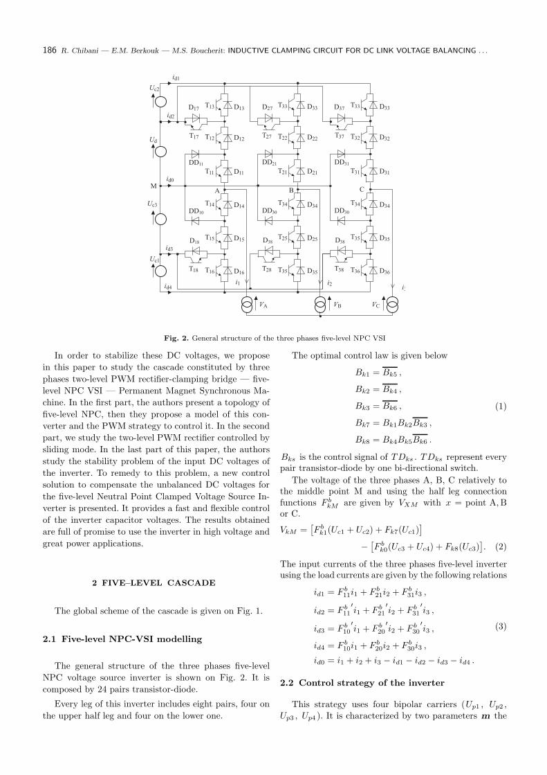
Fig. 2. General structure of the three phases five-level NPC VSI
In order to stabilize these DC voltages, we propose
in this paper to study the cascade constituted by three
phases two-level PWM rectifier-clamping bridge — five-
level NPC VSI — Permanent Magnet Synchronous Ma-
chine. In the first part, the authors present a topology of
five-level NPC, then they propose a model of this con-
verter and the PWM strategy to control it. In the second
part, we study the two-level PWM rectifier controlled by
sliding mode. In the last part of this paper, the authors
study the stability problem of the input DC voltages of
the inverter. To remedy to this problem, a new control
solution to compensate the unbalanced DC voltages for
the five-level Neutral Point Clamped Voltage Source In-
verter is presented. It provides a fast and flexible control
of the inverter capacitor voltages. The results obtained
are full of promise to use the inverter in high voltage and
great power applications.
2 FIVE–LEVEL CASCADE
The global scheme of the cascade is given on Fig. 1.
2.1 Five-level NPC-VSI modelling
The general structure of the three phases five-level
NPC voltage source inverter is shown on Fig. 2. It is
composed by 24 pairs transistor-diode.
Every leg of this inverter includes eight pairs, four on
the upper half leg and four on the lower one.
The optimal control law is given below
Bk1 = Bk5 ,
Bk2 = Bk4 ,
Bk3 = Bk6 ,
Bk7 = Bk1Bk2Bk3 ,
Bk8 = Bk4Bk5Bk6 .
(1)
Bks is the control signal of TDks . TDks represent everypair transistor-diode by one bi-directional switch.
The voltage of the three phases A, B, C relatively tothe middle point M and using the half leg connectionfunctions F b
kM are given by VXM with x = point A, Bor C.
VkM =[
F bk1(Uc1 + Uc2) + Fk7(Uc1)
]
−[
F bk0(Uc3 + Uc4) + Fk8(Uc3)
]
. (2)
The input currents of the three phases five-level inverterusing the load currents are given by the following relations
id1 = F b11i1 + F b
21i2 + F b31i3 ,
id2 = F b11
′
i1 + F b21
′
i2 + F b31
′
i3 ,
id3 = F b10
′
i1 + F b20
′
i2 + F b30
′
i3 ,
id4 = F b10i1 + F b
20i2 + F b30i3 ,
id0 = i1 + i2 + i3 − id1 − id2 − id3 − id4 .
(3)
2.2 Control strategy of the inverter
This strategy uses four bipolar carriers (Up1 , Up2 ,Up3 , Up4 ). It is characterized by two parameters m the

Journal of ELECTRICAL ENGINEERING 60, NO. 4, 2009 187
Fig. 3. Permanent Magnet Synchronous Machine speed control scheme based on sliding mode
Fig. 4. Structure of the two-level PWM current rectifier
index modulation and r the modulation rate. The al-gorithm of this strategy can be summarized as followsStep 1: Determination of the intermediate voltages
if Vrefk > Up1 then VkM1 = +Uc ,
if Vrefk < Up1 then VkM1 = 0 ,
if Vrefk > Up2 then VkM2 = +2Uc ,
if Vrefk < Up2 then VkM2 = +Uc ,
if Vrefk > Up3 then VkM3 = 0 ,
if Vrefk < Up3 then VkM3 = −Uc ,
if Vrefk > Up4 then VkM4 = −Uc ,
if Vrefk < Up4 then VkM4 = −2Uc .
(4)
Step 2: Determination of the output voltage
VkM = VkM1 + VkM2 + VkM3 + VkM4 . (5)
3 PERMANENT MAGNET
SYNCHRONOUS MACHINE MODELLING
The model of PMSM without damper winding hasbeen developed on rotor reference frame as follows [13–15]
[
Ud
Uq
]
=
[
Rs + Lds −ωLq
ωLd Rs + Lqs
] [
idiq
]
+
[
0ωKt
]
. (6)
The electric torque is stated as
Cem = Ktiq + (Ld − Lq)idiq , (7)
J(sω) = Cem − Cr − Kω . (8)
Control of PM motors is performed using field orientedcontrol for the operation of synchronous motor as a DCmotor. For the PM synchronous machine used, we developthe algorithm id = 0 (Fig. 3). When the d axis currentis equal to zero, the block diagram of the q axis becomessimilar to that of a DC machine and the speed can becontrolled by using a sliding mode controller which gen-erates the q axis voltage. We use a current regulator forthe d and q axes [13, 15].
4 TWO–LEVEL PWM CURRENT RECTIFIER
The general structure of the two-level PWM currentrectifier is given on the Fig. 4.
4.1 Voltage feedback control
For each phase k (k = 1, 2 or 3) of the three phasesnetwork feeding the rectifier considered can be repre-sented by a R, L circuit. Vresk is the voltage of one phasek of the three phases network and Vk is the voltage ofthe leg k of the rectifier.
The voltage loop imposes the effective value of thereference current of the network corresponding to thepower exchanged between the network and the continueload (Fig. 5).
Fig. 5. Control algorithm of the output DC voltage of the two-levelPWM current rectifier
Fig. 6. Control algorithm of the network current iresk of the two-
level PWM rectifier.

188 R. Chibani — E.M. Berkouk — M.S. Boucherit: INDUCTIVE CLAMPING CIRCUIT FOR DC LINK VOLTAGE BALANCING . . .
Fig. 7. Structure of the clamping bridge
Fig. 8. Output DC voltage, network voltage and current of thetwo-level PWM current rectifier: (a) – voltage Uc and its reference,
(b) – Vres1 , ires1 and its reference
We want to regulate the voltage Uc of the rectifier.For that we choose for sliding surface
S = Uc − Ucref . (9)Its derivative is
S = Uc , (10)
Uc =Ired − ich
C, (11)
Uc =1
C
(3VrIe
4Uc
− ich
)
. (12)
The condition ss < 0 insures the attractibility of thetrajectory towards the sliding surface. For that, we choose
s = −K1 sign(S) − k2S . (13)The output of the sliding mode controller gave
Ie = −4Uc
3Vr
[
C(
k1 sign(Uc − Ucref)+
k2(Uc − Ucref))
− ich
]
. (14)
4.2 Current feedback control
We control the network current of the phase 1 and 2by a Lyapunov function regulator. The algorithm of thiscurrent loop is given on the Fig. 6. In this scheme, thetransfer function H(p) is expressed as follows
H(s) =Iresk
V=
1
R + sL. (15)
From the network equations we have
Vres1 − VA = RIres1 + LIres1 ,
Vres2 − VB = RIres2 + LIres2 ,(16)
VA = Ng1Uc ,
VB = Ng2Uc .(17)
We choose the following sliding surfaces
S1 = Ires1 − Iref1 ,
S2 = Ires2 − Iref2 .(18)
To satisfy the attractability condition, we choose
S1 = −k11 sign(S1) − k21S1 ,
S2 = −k12 sign(S2) − k22S2 ,
Sk = Iresk −√
2ωIe cos(
ωt −2(k − 1)π
3
) (19)
with k = 1, 2, 3.We obtain
Ng1 =1
4Uc
[
Vres1 − RIres1 + Lk11 sign(Ires1 − Iref1)
+ Lk21(Ires1 − Iref1) −√
2LωIe cos(ωt)]
,
Ng2 =1
4Uc
[
Vres2 − RIres2 + Lk12 sign(Ires2 − Iref2)
+ Lk22(Ires2 − Iref2) −√
2LωIe cos(ωt)]
,
(20)
5 CLAMPING BRIDGE
In order to remedy to the unbalance problem, we sug-gest a solution which consists in establish a bridge bal-ancing between the rectifier and the intermediate filter(Fig. 7). The aim of this use is to limit and stabilise vari-ations of the input DC voltage of the inverter.
A cell equalization scheme for capacitors has been pro-posed to equalize input DC voltages. The capacitor volt-age equalization clamping bridge scheme has many ad-vantages such as higher equalization efficiency and a mod-ular design approach.
Capacitor voltage equalization control should be im-plemented to restrict the charge-discharge current to theallowable cell limitations in the capacitor string.
The balancing algorithms search to efficiently removeenergy from a strong capacitor and transfer that energyinto a weak one until the capacitor voltage is equalizedacross all capacitors.
Every switch Tx (x = 1, 2, 3, 4) represents a pairtransistor-diode.
Journal of ELECTRICAL ENGINEERING 60, NO. 4, 2009 189
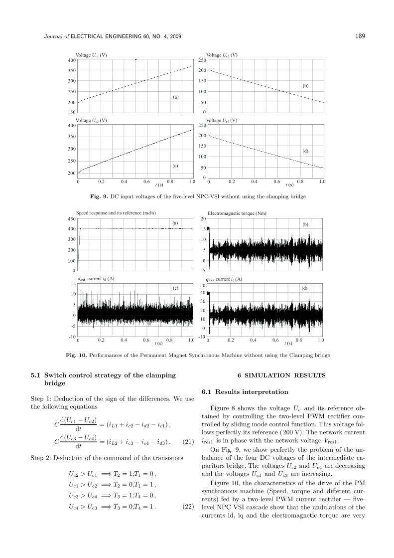
Fig. 9. DC input voltages of the five-level NPC-VSI without using the clamping bridge
Fig. 10. Performances of the Permanent Magnet Synchronous Machine without using the Clamping bridge
5.1 Switch control strategy of the clamping
bridge
Step 1: Deduction of the sign of the differences. We usethe following equations
Cd(Uc1 − Uc2)
dt= (iL1 + ic2 − id2 − ic1) ,
Cd(Uc3 − Uc4)
dt= (iL2 + ic3 − ic4 − id3) . (21)
Step 2: Deduction of the command of the transistors
Uc2 > Uc1 =⇒ T2 = 1;T1 = 0 ,
Uc1 > Uc2 =⇒ T2 = 0;T1 = 1 ,
Uc3 > Uc4 =⇒ T3 = 1;T4 = 0 ,
Uc4 > Uc3 =⇒ T3 = 0;T4 = 1 . (22)
6 SIMULATION RESULTS
6.1 Results interpretation
Figure 8 shows the voltage Uc and its reference ob-tained by controlling the two-level PWM rectifier con-trolled by sliding mode control function. This voltage fol-lows perfectly its reference (200 V). The network currentires1 is in phase with the network voltage Vres1 .
On Fig. 9, we show perfectly the problem of the un-balance of the four DC voltages of the intermediate ca-pacitors bridge. The voltages Uc2 and Uc4 are decreasingand the voltages Uc1 and Uc3 are increasing.
Figure 10, the characteristics of the drive of the PMsynchronous machine (Speed, torque and different cur-rents) fed by a two-level PWM current rectifier — five-level NPC VSI cascade show that the undulations of thecurrents id, iq and the electromagnetic torque are very
190 R. Chibani — E.M. Berkouk — M.S. Boucherit: INDUCTIVE CLAMPING CIRCUIT FOR DC LINK VOLTAGE BALANCING . . .
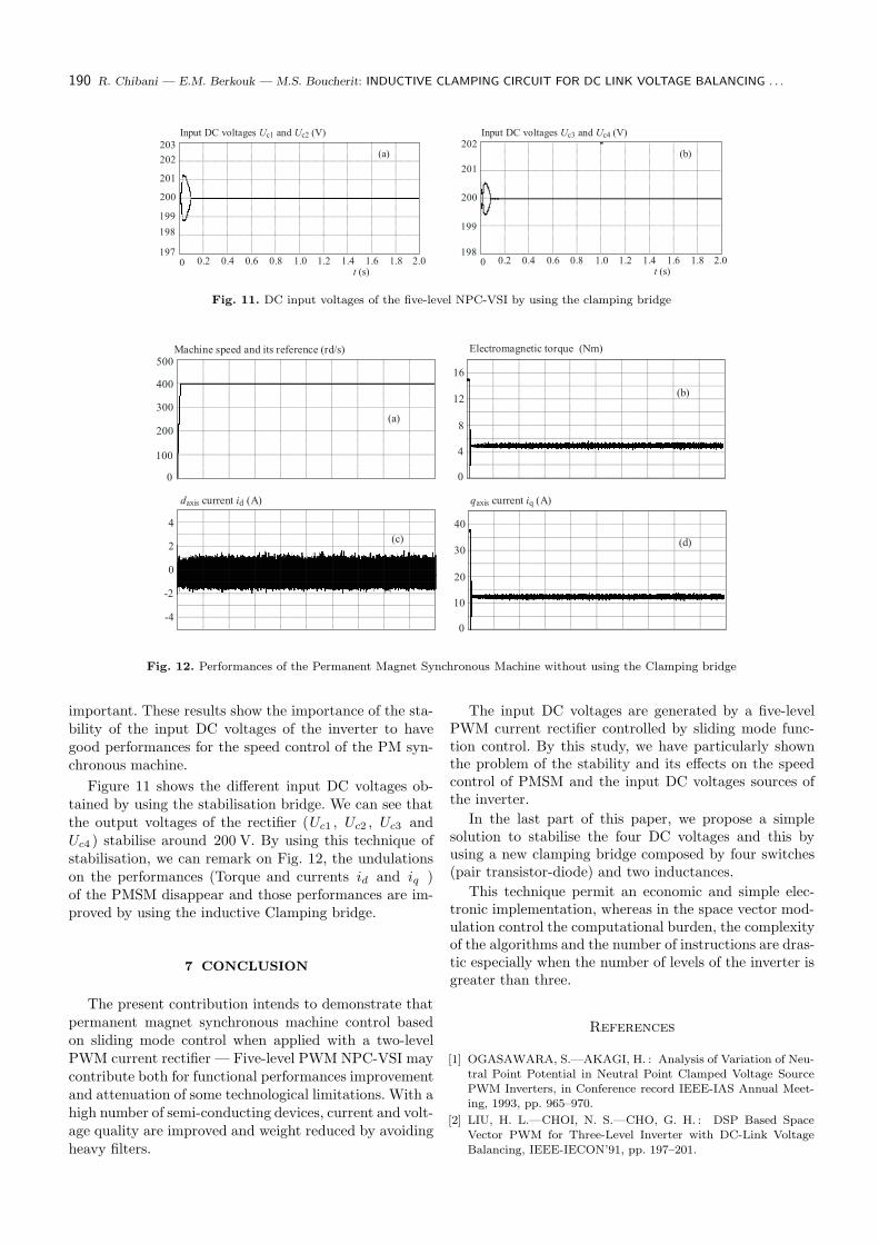
Fig. 11. DC input voltages of the five-level NPC-VSI by using the clamping bridge
Fig. 12. Performances of the Permanent Magnet Synchronous Machine without using the Clamping bridge
important. These results show the importance of the sta-bility of the input DC voltages of the inverter to havegood performances for the speed control of the PM syn-chronous machine.
Figure 11 shows the different input DC voltages ob-tained by using the stabilisation bridge. We can see thatthe output voltages of the rectifier (Uc1 , Uc2 , Uc3 andUc4 ) stabilise around 200 V. By using this technique ofstabilisation, we can remark on Fig. 12, the undulationson the performances (Torque and currents id and iq )of the PMSM disappear and those performances are im-proved by using the inductive Clamping bridge.
7 CONCLUSION
The present contribution intends to demonstrate thatpermanent magnet synchronous machine control basedon sliding mode control when applied with a two-levelPWM current rectifier — Five-level PWM NPC-VSI maycontribute both for functional performances improvementand attenuation of some technological limitations. With ahigh number of semi-conducting devices, current and volt-age quality are improved and weight reduced by avoidingheavy filters.
The input DC voltages are generated by a five-levelPWM current rectifier controlled by sliding mode func-tion control. By this study, we have particularly shownthe problem of the stability and its effects on the speedcontrol of PMSM and the input DC voltages sources ofthe inverter.
In the last part of this paper, we propose a simplesolution to stabilise the four DC voltages and this byusing a new clamping bridge composed by four switches(pair transistor-diode) and two inductances.
This technique permit an economic and simple elec-tronic implementation, whereas in the space vector mod-ulation control the computational burden, the complexityof the algorithms and the number of instructions are dras-tic especially when the number of levels of the inverter isgreater than three.
References
[1] OGASAWARA, S.—AKAGI, H. : Analysis of Variation of Neu-tral Point Potential in Neutral Point Clamped Voltage SourcePWM Inverters, in Conference record IEEE-IAS Annual Meet-ing, 1993, pp. 965–970.
[2] LIU, H. L.—CHOI, N. S.—CHO, G. H. : DSP Based SpaceVector PWM for Three-Level Inverter with DC-Link Voltage
Balancing, IEEE-IECON’91, pp. 197–201.

Journal of ELECTRICAL ENGINEERING 60, NO. 4, 2009 191
[3] MENZIES, H.—STEIMER, P.—STEINKE, J. K. : Five-Level
GTO Inverters for Large Induction Motor Drives, Conference
record IEEE-IAS Annual Meeting, 1993, pp. 595–601.
[4] LEE, D. H.—LEE, S. R.—LEE, F. C. : An Analysis of Mid-
point Balance for the Neutral-Point-Clamped Three-Level VSI,
IEEE-PESC’98, pp. 193–199.
[5] KOYAMA, M.—FUJII, T.—UCHIDA, R.—KAWABATA, T. :
Space Voltage Vector Based New PWM Method for Large Ca-
pacity Three-Level GTO Inverter, in Proc. IEEE IECON’92,
1992, pp. 271-276.
[6] CELANOVIC, N.—BOROJEVIC, D. : A Comprehensive Study
of Neutral Point Voltage Balancing Problem in Three-Level
Neutral-Point-Clamped Voltage Source PWM Inverters, IEEE
Trans. Power Electron. 15 (Mar 2000), 242-249.
[7] FRACCHIA, M.—GHIARA, T.—MARCHESONI, M.—MAZ-
ZUCCHELLI, M. : Optimized Modulation Techniques for the
Generalized n-Level Converter, PESC’92 Conference Record,
Toledo, Spain, June/July 1992, pp. 1205–1213.
[8] PURKIAT, P.—SRIAMAKAVACHAM, R. S. : A New Gener-
alized Space Vector Modulation Algorithm for Neutral-Point-
Clamped Multilevel Converters, Progress in Electromagnet-
ics Research Symposium, Cambridge, USA, 26-29 Mar 2006,
pp. 330–335.
[9] BENDRE, A.—KRSTIC, S.—VANDER MEER, J.—VENKA-
TARAMANAN, G. : Comparative Evaluation of Modulation
Algorithms for Neutral-Point-Clamped Converters, IEEE Trans-
actions on Industry Applications 41 No. 2 (Mar/Apr 2005),
634–643.
[10] PAN, Z.—PENG, F. Z.—CORZINE, K. A.—STEFANOVIC,
V. R.—LEUTHEN, J. M.—GATARIC, S. : Voltage Balanc-
ing Control of Diode Clamped Multilevel Rectifier/Inverter Sys-
tems, IEEE Transactions on Industry Applications 41 No. 6
(Nov/Dec 2005), 1698–1706.
[11] BENDRE, A.—VENKATARAMANAN, G.—ROSENE, D.—
SRINIVASAN, V. : Modelling and Design of Neutral-Point Volt-
age Regulator for a Three-Level DiodeClamped Inverter using
Multiple-Carrier Modulation, IEEE Transactions on Industrial
Electronics 53 No. 3 (June 2006), 718–726.
[12] VENKATESHMARHU, S.—MUNI, B. P.—RAJKUMAR, A.
D.—PRAVEEN, J. : Direct Power Control Strategies for Mul-
tilevel Inverter Based Custom Power Devices, Proceeding of
the World Academy of Science, Engineering and Technology 29
(May 2008), 205–213.
[13] CHIBANI, R.—BERKOUK, E. M. : Five-Level PWM Cur-
rent Rectifier – Five-level NPC VSI – Permanent Magnet Syn-
chronous Machine Cascade, European Physical Journal — Ap-plied Physics No. 30 (May 2005), 135–148.
[14] CHIBANI, R.—BERKOUK, E. M.—BOUCHERIT, M. S. :
Lyapunov Control of Three-Level PWM Rectifiers to Equili-
brate Input DC Voltages of Five-Level NPC-VSI, International
Review of Electrical Engineering 2 No. 1 (Jan-Feb 2007), 36–49.
[15] KRAUSE, P. C. : Analysis of Electric Machinery, McGrawHill,
New York, 1986.
Received 31 October 2008
Chibani Redha was born in Algiers, Algeria, in 1970. Hereceived the Engineer degree in 1993 from the National Schoolof engineers and technicians of Algeria, the Magister degree in1999 and the Doctorat (PhD) in 2007 from National Polytech-nic School of Algiers, Algeria all in Electrical Engineering. Hiscurrent research interests are in the area of power electronics,electrical drives and process control.
El Madjid Berkouk was born in Bejaıa, Algeria, in 1968.He received the Engineer degree in 1991 in electrical engineer-ing from the Polytechnic National School of Algiers, Algeria.In 1993 and 1995, he obtained respectively the Master of Sci-ence in ENSEEIHT (Toulouse) and PhD in CNAM (Paris).From 1993 to 1996, he was teaching at university of Paris XI.Since 1996, he was with National Polytechnic School Nationalof Algiers as associated Professor. His current research inter-ests are in power electronics and electrical drives.
Boucherit Mohamed Seghir was born in 1954 in Al-giers. He received the Engineer degree in Electrotechnics, theMagister degree and the Doctorat d’Etat (PhD) in electricalengineering, from the National Polytechnic School of Algiers,Algeria, in 1980, 1988 and 1995 respectively. Upon graduation,he joined the Electrical Engineering Department of Polytech-nic National School. He is a Professor, member of ProcessControl Laboratory and his research interests are in the areaof electrical drives and process control.