Embed Size (px)
Citation preview

V+
OUT
GND IN-
IN+
CBYPASS
0.01 Fm
to
0.1 Fm
2.7 V to 26 V
REF
Reference
Voltage
Supply LoadRSHUNT
Output
R1 R3
R2 R4
Product
Folder
Order
Now
Technical
Documents
Tools &
Software
Support &Community
ReferenceDesign
An IMPORTANT NOTICE at the end of this data sheet addresses availability, warranty, changes, use in safety-critical applications,intellectual property matters and other important disclaimers. PRODUCTION DATA.
English Data Sheet: SBOS469
INA199ZHCS912G –APRIL 2009–REVISED FEBRUARY 2017
INA199 26V、、双双向向、、零零漂漂移移、、低低侧侧或或高高侧侧、、电电压压输输出出、、电电流流分分流流监监控控器器
1
1 特特性性
1• 宽共模范围:–0.3V 至 26V• 偏移电压:±150μV(最大值)
(支持 10mV 满量程分流压降)
• 精度:
– 增益误差(最大过热误差):
– ±1%(C 版本)
– ±1.5%(A 和 B 版本)
– 0.5µV/°C 偏移漂移(最大值)
– 10ppm/°C 增益漂移(最大值)
• 增益选择:
– INA199x1:50V/V– INA199x2:100V/V– INA199x3:200V/V
• 静态电流:100μA(最大值)
• 封装:6 引脚 SC70、10 引脚 UQFN
2 应应用用
• 笔记本电脑
• 手机
• 符合 Qi 标准的无线充电发送器
• 电信设备
• 电源管理
• 电池充电器
3 说说明明
INA199 系列电压输出、电流分流监控器(也称为电流
传感放大器)常用于过流保护、针对系统优化的精密电
流测量或闭环反馈电路。该系列器件可在独立于电源电
压的 –0.3V 至 26V 共模电压下感应分流电阻器上的电
压降。共有三种固定增益可供选择:50V/V、100V/V和 200V/V。该系列器件采用零漂移架构,偏移较低,
因此在进行电流感测时能够将分流电阻器两端的最大压
降保持在最低 10mV 的满量程。
这些器件由 2.7V 至 26V 的单个电源供电,消耗的最
大电源电流为 100µA。所有版本的额定温度均为
–40°C 至 125°C,并且提供了 SC70-6 和薄型 UQFN-10 两种封装。
器器件件信信息息(1)
器器件件型型号号 封封装装 封封装装尺尺寸寸((标标称称值值))
INA199SC70 (6) 2.00mm × 1.25mmUQFN (10) 1.80mm x 1.40mm
(1) 要了解所有可用封装,请参见数据表末尾的可订购产品附录。
简简化化电电路路原原理理图图

2
INA199ZHCS912G –APRIL 2009–REVISED FEBRUARY 2017 www.ti.com.cn
版权 © 2009–2017, Texas Instruments Incorporated
目目录录
1 特特性性.......................................................................... 12 应应用用.......................................................................... 13 说说明明.......................................................................... 14 修修订订历历史史记记录录 ........................................................... 25 Device Comparison Table ..................................... 46 Pin Configuration and Functions ......................... 47 Specifications......................................................... 5
7.1 Absolute Maximum Ratings ...................................... 57.2 ESD Ratings.............................................................. 57.3 Recommended Operating Conditions....................... 67.4 Thermal Information .................................................. 67.5 Electrical Characteristics........................................... 77.6 Typical Characteristics .............................................. 8
8 Detailed Description ............................................ 128.1 Overview ................................................................. 128.2 Functional Block Diagram ....................................... 128.3 Feature Description................................................. 13
8.4 Device Functional Modes........................................ 149 Application and Implementation ........................ 19
9.1 Application Information............................................ 199.2 Typical Applications ................................................ 19
10 Power Supply Recommendations ..................... 2211 Layout................................................................... 22
11.1 Layout Guidelines ................................................. 2211.2 Layout Example .................................................... 22
12 器器件件和和文文档档支支持持 ..................................................... 2312.1 文档支持 ................................................................ 2312.2 接收文档更新通知 ................................................. 2312.3 社区资源 ................................................................ 2312.4 商标 ....................................................................... 2312.5 静电放电警告......................................................... 2312.6 Glossary ................................................................ 23
13 机机械械、、封封装装和和可可订订购购信信息息....................................... 23
4 修修订订历历史史记记录录注:之前版本的页码可能与当前版本有所不同。
Changes from Revision F (June 2016) to Revision G Page
• 已更改 精度 特性 项目的第一个子项目:从子项目中删除了 ±1.5% 并增加了版本差异.......................................................... 1• 已更改 105°C 至 125°C(在说明部分的最后一段) ............................................................................................................... 1• Added INA199Cx to last row of Analog inputs in Absolute Maximum Ratings table.............................................................. 5• Changed INA199Ax HBM value from ±4000 to ±2000 and changed INA199B1, INA199B2, and INA199B3 to
INA199Bx and INA199Cx in second V(ESD) section of ESD Ratings table ............................................................................. 5• Changed maximum specification from 105 to 125 in TA row of Recommended Operating Conditions table ........................ 6• Changed all TA = –40°C to 105°C to TA = –40°C to 125°C in Electrical Characteristics table .............................................. 7• Added version C to last row of VCM parameter in Electrical Characteristics table ................................................................ 7• Added versions A and B to first Gain error parameter row, added second row .................................................................... 7• Changed devices listed in test conditions of GBW parameter in Electrical Characteristics table to INA199x1,
INA199x2, and INA199x3, respectively for the three rows..................................................................................................... 7• Changed maximum specification from 105 to 125 in Specified range parameter of Electrical Characteristics table ............ 7• Changed 105°C to 125°C in last paragraph of Overview section ........................................................................................ 12• Changed INA199A2 and INA199B2 to INA199x2 and changed INA199A2 and INA199B2 to INA199x2 in last
paragraph of Input Filtering section...................................................................................................................................... 15• Changed listed products in table of Figure 22 ..................................................................................................................... 15• Changed version B to version B and C in second paragraph of Improving Transient Robustness section ........................ 18
Changes from Revision E (December 2015) to Revision F Page
• 在封装 特性 项目中添加了两种封装的引脚数量...................................................................................................................... 1• 已删除最后一项应用要点 ........................................................................................................................................................ 1• 已更改说明部分中的第二句) ................................................................................................................................................. 1• Changed Analog inputs parameter in Absolute Maximum Ratings table ............................................................................... 5• Changed ESD Ratings table: deleted both Machine model rows, changed INA199B HBM specification ............................. 5• Changed Electrical Characteristics table: recombined the two Electrical Characteristics tables into one ............................ 7

3
INA199www.ti.com.cn ZHCS912G –APRIL 2009–REVISED FEBRUARY 2017
Copyright © 2009–2017, Texas Instruments Incorporated
• Added minimum specification to second row of Power Supply, VS parameter in Electrical Characteristics table ................ 7• Added θJA parameter back to Electrical Characteristics table ............................................................................................... 7
Changes from Revision D (November 2012) to Revision E Page
• 已添加 ESD 额定值表、热性能信息表、特性 说明 部分、器件功能模式、应用和实施部分、电源相关建议部分、布局部分、器件和文档支持部分以及机械、封装和可订购信息部分 .............................................................................................. 1
Changes from Revision C (August 2012) to Revision D Page
• Changed Frequency Response, Bandwidth parameter in Electrical Characteristics table .................................................... 7• Updated Figure 21................................................................................................................................................................ 14• Updated Figure 22................................................................................................................................................................ 15
Changes from Revision B (February 2010) to Revision C Page
• 已添加 INA199Bx 增益至第四个 特性 项目............................................................................................................................. 1• Added INA199Bx data to Product Family Table..................................................................................................................... 4• Added INA199Bx data to Package Information table ............................................................................................................. 4• Added silicon version B data to Input, Common-Mode Input Range parameter of Electrical Characteristics table .............. 7• Added QFN package information to Temperature Range section of Electrical Characteristics table.................................... 7• Updated Figure 3.................................................................................................................................................................... 8• Updated Figure 9.................................................................................................................................................................... 9• Updated Figure 12.................................................................................................................................................................. 9• Changed last paragraph of the Selecting RS section to cover both INA199Ax and INA199Bx versions ............................. 13• Changed Input Filtering section............................................................................................................................................ 14• Added Improving Transient Robustness section.................................................................................................................. 18
Changes from Revision A (June 2009) to Revision B Page
• Deleted ordering information content from Package/Ordering table ...................................................................................... 4• Updated DCK pinout drawing ................................................................................................................................................. 4
Changes from Original (April 2009) to Revision A Page
• Added ordering number and transport media, quantity columns to Package/Ordering Information table ............................. 4

NC(1)
V+
NC(1)
IN+
IN+
IN-
IN-
REF 8
9
10
5
4
31 2
7 6
GND
OUT
1
2
3
6
5
4
OUT
IN-
IN+
REF
GND
V+
4
INA199ZHCS912G –APRIL 2009–REVISED FEBRUARY 2017 www.ti.com.cn
Copyright © 2009–2017, Texas Instruments Incorporated
5 Device Comparison Table
PRODUCT GAIN R3 AND R4 R1 AND R2
INA199x1 50 20 kΩ 1 MΩINA199x2 100 10 kΩ 1 MΩINA199x3 200 5 kΩ 1 MΩ
6 Pin Configuration and Functions
DCK Package6-Pin SC70Top View
RSW Package10-Pin UQFN
Top View
(1) NC denotes no internal connection. These pins can be left floating or connected to any voltage between GND and V+.
Pin FunctionsPIN
I/O DESCRIPTIONNAME SC70 UQFNGND 2 9 Analog GroundIN– 5 4, 5 Analog input Connect to load side of shunt resistor.IN+ 4 2, 3 Analog input Connect to supply side of shunt resistor.NC — 1, 7 — Not internally connected. Leave floating or connect to ground.OUT 6 10 Analog output Output voltageREF 1 8 Analog input Reference voltage, 0 V to V+V+ 3 6 Analog Power supply, 2.7 V to 26 V

5
INA199www.ti.com.cn ZHCS912G –APRIL 2009–REVISED FEBRUARY 2017
Copyright © 2009–2017, Texas Instruments Incorporated
(1) Stresses beyond those listed under Absolute Maximum Ratings may cause permanent damage to the device. These are stress ratingsonly, which do not imply functional operation of the device at these or any other conditions beyond those indicated under RecommendedOperating Conditions. Exposure to absolute-maximum-rated conditions for extended periods may affect device reliability.
(2) VIN+ and VIN– are the voltages at the IN+ and IN– pins, respectively.(3) Input voltage at any pin c an exceed the voltage shown if the current at that pin is limited to 5 mA.
7 Specifications
7.1 Absolute Maximum Ratingsover operating free-air temperature range (unless otherwise noted) (1)
MIN MAX UNITSupply voltage 26 V
Analog inputs, VIN+, VIN–(2)
Differential (VIN+) – (VIN–) –26 26VCommon-mode (3), INA199Ax GND – 0.3 26
Common-mode (3), INA199Bx and INA199Cx GND – 0.1 26REF input GND – 0.3 (V+) + 0.3 VOutput (3) GND – 0.3 (V+) + 0.3 VInput current Into all pins (3) 5 mAOperating temperature –40 125 °CJunction temperature 150 °CStorage temperature, Tstg –65 150 °C
(1) JEDEC document JEP155 states that 500-V HBM allows safe manufacturing with a standard ESD control process.(2) JEDEC document JEP157 states that 250-V CDM allows safe manufacturing with a standard ESD control process.
7.2 ESD RatingsVALUE UNIT
INA199A1, INA199A2, and INA199A3 in DCK and RSW Packages
V(ESD) Electrostatic dischargeHuman-body model (HBM), per ANSI/ESDA/JEDEC JS-001 (1) ±2000
VCharged-device model (CDM), per JEDEC specification JESD22-C101 (2) ±1000
INA199Bx and INA199Cx in DCK and RSW Packages
V(ESD) Electrostatic dischargeHuman-body model (HBM), per ANSI/ESDA/JEDEC JS-001 (1) ±3500
VCharged-device model (CDM), per JEDEC specification JESD22-C101 (2) ±1000

6
INA199ZHCS912G –APRIL 2009–REVISED FEBRUARY 2017 www.ti.com.cn
Copyright © 2009–2017, Texas Instruments Incorporated
7.3 Recommended Operating Conditionsover operating free-air temperature range (unless otherwise noted)
MIN NOM MAX UNITVCM Common-mode input voltage 12 VVS Operating supply voltage (applied to V+) 5 VTA Operating free-air temperature –40 125 °C
(1) For more information about traditional and new thermal metrics, see the Semiconductor and IC Package Thermal Metrics applicationreport.
7.4 Thermal Information
THERMAL METRIC (1)INA199
UNITDCK (SC70) RSW (UQFN)6 PINS 10 PINS
RθJA Junction-to-ambient thermal resistance 227.3 107.3 °C/WRθJC(top) Junction-to-case (top) thermal resistance 79.5 56.5 °C/WRθJB Junction-to-board thermal resistance 72.1 18.7 °C/WψJT Junction-to-top characterization parameter 3.6 1.1 °C/WψJB Junction-to-board characterization parameter 70.4 18.7 °C/WRθJC(bot) Junction-to-case (bottom) thermal resistance — — °C/W

7
INA199www.ti.com.cn ZHCS912G –APRIL 2009–REVISED FEBRUARY 2017
Copyright © 2009–2017, Texas Instruments Incorporated
(1) RTI = Referred-to-input.(2) See Typical Characteristic curve, Output Voltage Swing vs Output Current (Figure 6).
7.5 Electrical Characteristicsat TA = 25°C, VS = 5 V, VIN+ = 12 V, VSENSE = VIN+ – VIN–, and VREF = VS / 2 (unless otherwise noted)
PARAMETER TEST CONDITIONS MIN TYP MAX UNITINPUT
VCM Common-mode input rangeVersion A, TA = –40°C to 125°C –0.3 26
VVersion B and C, TA = –40°C to 125°C –0.1 26
CMR Common-mode rejection VIN+ = 0 V to 26 V, VSENSE = 0 mV,TA = –40°C to 125°C 100 120 dB
VOS Offset voltage, RTI (1) VSENSE = 0 mV ±5 ±150 μVdVOS/dT VOS vs temperature TA = –40°C to 125°C 0.1 0.5 μV/°C
PSR Power supply rejection VS = 2.7 V to 18 V,VIN+ = 18 V, VSENSE = 0 mV ±0.1 μV/V
IB Input bias current VSENSE = 0 mV 28 μAIOS Input offset current VSENSE = 0 mV ±0.02 μAOUTPUT
G GainINA199x1 50
V/VINA199x2 100INA199x3 200
Gain error
Version A and B, VSENSE = –5 mV to5 mV, TA = –40°C to 125°C ±0.03% ±1.5%
Version C, VSENSE = –5 mV to 5 mV,TA = –40°C to 125°C ±0.03% ±1%
Gain error vs temperature TA = –40°C to 125°C 3 10 ppm/°CNonlinearity error VSENSE = –5 mV to 5 mV ±0.01%Maximum capacitive load No sustained oscillation 1 nF
VOLTAGE OUTPUT (2)
Swing to V+ power-supply rail RL = 10 kΩ to GND, TA = –40°C to 125°C (V+) –0.05
(V+) –0.2 V
Swing to GND RL = 10 kΩ to GND, TA = –40°C to 125°C (VGND) +0.005
(VGND) +0.05 V
FREQUENCY RESPONSE
GBW BandwidthCLOAD = 10 pF, INA199x1 80
kHzCLOAD = 10 pF, INA199x2 30CLOAD = 10 pF, INA199x3 14
SR Slew rate 0.4 V/μsNOISE, RTI (1)
Voltage noise density 25 nV/√HzPOWER SUPPLY
VS Operating voltage rangeTA = –40°C to 125°C 2.7 26
V–20°C to 85°C 2.5 26
IQ Quiescent current VSENSE = 0 mV 65 100 μAIQ over temperature TA = –40°C to 125°C 115 μA
TEMPERATURE RANGESpecified range –40 125 °COperating range –40 125 °C
θJA Thermal resistanceSC70 250
°C/WUQFN 80

V+
(V+) 0.5-
(V+) 1.0-
(V+) 1.5-
(V+) 2.0-
(V+) 2.5-
(V+) 3.0-
Ou
tpu
t V
olta
ge
Sw
ing
(V
)
GND + 3.0
GND + 2.5
GND + 2.0
GND + 1.5
GND + 1.0
GND + 0.5
GND
0 5 10 15 20
Output Current (mA)
25 30 35 40
V = 2.7VS
to 26V
V = 2.7V to 26VS
V = 5V to 26VS
V = 2.7VS
T = 40 C- °A
T = +25 C°A
T = +105 C°A
Frequency (Hz)
|CM
RR
| (d
B)
160
140
120
100
80
60
40
20
01 10 1M100 1k 10k 100k
V = +5V
V = 1V Sine
V = Shorted
V = 2.5V
S
CM
DIF
REF
Frequency (Hz)
Ga
in (
dB
)
70
60
50
40
30
20
10
0
10-
10 100 10M1k 10k 100k 1M
V = 0V
V = 15mV SineCM
DIF PP
G = 50
G = 200
G = 100
Frequency (Hz)
|PS
R| (d
B)
160
140
120
100
80
60
40
20
0
1 10 100k
V = 5 V + 250-mV sine disturbanceS
V = 0 VCM
V = ShortedDIF
V = 2.5 VREF
100 1k 10k
Temperature ( C)°
Off
se
t V
olta
ge
(V
)m
20
15
10
5
0
5
10
15
20
-
-
-
-
-50 -25 1250 25 50 75 100
Temperature ( C)°
CM
RR
(V
/V)
m
1.0
0.8
0.6
0.4
0.2
0
0.2
0.4
0.6
0.8
1.0
-
-
-
-
--50 -25 1250 25 50 75 100
8
INA199ZHCS912G –APRIL 2009–REVISED FEBRUARY 2017 www.ti.com.cn
Copyright © 2009–2017, Texas Instruments Incorporated
7.6 Typical Characteristicsperformance measured with the INA199A3 at TA = 25°C, VS = 5 V, VIN+ = 12 V, and VREF = VS / 2 (unless otherwise noted)
Figure 1. Offset Voltage vs Temperature Figure 2. Common-Mode Rejection Ratio vs Temperature
Figure 3. Gain vs Frequency Figure 4. Power-Supply Rejection Ratio vs Frequency
Figure 5. Common-Mode Rejection Ratio vs Frequency Figure 6. Output Voltage Swing vs Output Current

Temperature ( C)°
Quie
scent C
urr
ent (
A)
m
70
68
66
64
62
60-50 -25 1250 25 50 75 100
Frequency (Hz)
Input-
Refe
rred V
oltage N
ois
e (
nV
/)
ÖH
z
100
10
1
10 100 1k 100k10k
V = 2.5V±S
V = 0VREF
V , V = 0VIN IN+-
G = 50
G = 100 G = 200
Common-Mode Voltage (V)
Inp
ut
Bia
s C
urr
en
t (
A)
m
30
25
20
15
10
5
0
-5
0 5 3010 15 20 25
I , V = 2.5VB+ REF
I , I , V = 0V
andI , V = 2.5V
B+ B REF-
B REF-
Temperature ( C)°
Inp
ut
Bia
s C
urr
en
t (
A)
m
30
29
28
27
26
25-50 -25 1250 25 50 75 100
V+
(V+) 0.25-
(V+) 0.50-
(V+) 0.75-
(V+) 1.00-
(V+) 1.25-
(V+) 1.50-
Ou
tpu
t V
olta
ge
(V
)
GND + 1.50
GND + 1.25
GND + 1.00
GND + 0.75
GND + 0.50
GND + 0.25
GND
0 2 4 5 8
Output Current (mA)
10 12 14 1816
+85 C°
+25 C°
-20 C°
+85 C°
- °20 C
+25 C°
Common-Mode Voltage (V)
Inp
ut
Bia
s C
urr
en
t (
A)
m
50
40
30
20
10
0
-10
0 5 3010 15 20 25
I , I , V = 2.5VB+ B REF-
I , I , V = 0VB+ B REF-
9
INA199www.ti.com.cn ZHCS912G –APRIL 2009–REVISED FEBRUARY 2017
Copyright © 2009–2017, Texas Instruments Incorporated
Typical Characteristics (continued)performance measured with the INA199A3 at TA = 25°C, VS = 5 V, VIN+ = 12 V, and VREF = VS / 2 (unless otherwise noted)
VS = 2.5 V
Figure 7. Output Voltage Swing vs Output Current Figure 8. Input Bias Current vs Common-Mode VoltageWith Supply Voltage = 5 V
Figure 9. Input Bias Current vs Common-Mode VoltageWith Supply Voltage = 0 V (Shutdown)
Figure 10. Input Bias Current vs Temperature
Figure 11. Quiescent Current vs Temperature Figure 12. Input-Referred Voltage Noise vs Frequency

2V
/div
Time (250ms/div)
0V
V = 5V, V = 12V, V = 2.5VS CM REF
Noninverting Input Overload
Output
1V
/div
Time (100 s/div)m
0V
Output Voltage
Supply Voltage
V = 5V, 1kHz Step with V = 0V, V = 2.5VS DIFF REF
Co
mm
on
-Mo
de
Vo
lta
ge
(1
V/d
iv)
Ou
tpu
t Vo
ltag
e (4
0m
V/d
iv)
Time (50ms/div)
Common Voltage Step
0V
0V
Output Voltage
2V
/div
Time (250ms/div)
0V
Output
V = 5V, V = 12V, V = 2.5VS CM REF
Inverting Input Overload
Re
ferr
ed
-to
-In
pu
t
Vo
lta
ge
No
ise
(2
00
nV
/div
)
Time (1s/div)
V = 2.5V±S
V = 0VCM
V = 0VDIF
V = 0VREF
Ou
tpu
t V
olta
ge
(0.5
V/d
iV)
Inp
ut
Vo
lta
ge
(5m
V/d
iV)
Time (100ms/div)
2VPP Output Signal
10mV Input SignalPP
10
INA199ZHCS912G –APRIL 2009–REVISED FEBRUARY 2017 www.ti.com.cn
Copyright © 2009–2017, Texas Instruments Incorporated
Typical Characteristics (continued)performance measured with the INA199A3 at TA = 25°C, VS = 5 V, VIN+ = 12 V, and VREF = VS / 2 (unless otherwise noted)
Figure 13. 0.1-Hz to 10-Hz Voltage Noise (Referred-to-Input) Figure 14. Step Response (10-mVPP Input Step)
Figure 15. Common-Mode Voltage Transient Response Figure 16. Inverting Differential Input Overload
Figure 17. Noninverting Differential Input Overload Figure 18. Start-Up Response

1V
/div
Time (100ms/div)
0VV = 5V, 1kHz Step with V = 0V, V = 2.5VS DIFF REF
Supply Voltage
Output Voltage
11
INA199www.ti.com.cn ZHCS912G –APRIL 2009–REVISED FEBRUARY 2017
Copyright © 2009–2017, Texas Instruments Incorporated
Typical Characteristics (continued)performance measured with the INA199A3 at TA = 25°C, VS = 5 V, VIN+ = 12 V, and VREF = VS / 2 (unless otherwise noted)
Figure 19. Brownout Recovery

-
+
IN-
IN+
REF
GND
V+
OUT
Copyright © 2017, Texas Instruments Incorporated
12
INA199ZHCS912G –APRIL 2009–REVISED FEBRUARY 2017 www.ti.com.cn
Copyright © 2009–2017, Texas Instruments Incorporated
8 Detailed Description
8.1 OverviewThe INA199 is a 26-V common mode, zero-drift topology, current-sensing amplifier that can be used in both low-side and high-side configurations. The device is a specially-designed, current-sensing amplifier that is able toaccurately measure voltages developed across a current-sensing resistor on common-mode voltages that farexceed the supply voltage powering the device. Current can be measured on input voltage rails as high as 26 Vand the device can be powered from supply voltages as low as 2.7 V.
The zero-drift topology enables high-precision measurements with maximum input offset voltages as low as150 µV with a maximum temperature contribution of 0.5 µV/°C over the full temperature range of –40°C to+125°C.
8.2 Functional Block Diagram

ADC
Power Supply Load
RSHUNT
CBYPASS
0.1 µF
5-V Supply
-
+
IN-
IN+
GND
V+
OUT
REF
Microcontroller
Copyright © 2017, Texas Instruments Incorporated
13
INA199www.ti.com.cn ZHCS912G –APRIL 2009–REVISED FEBRUARY 2017
Copyright © 2009–2017, Texas Instruments Incorporated
8.3 Feature Description
8.3.1 Basic ConnectionsFigure 20 shows the basic connections for the INA199. The input pins, IN+ and IN–, must be connected as closeas possible to the shunt resistor to minimize any resistance in series with the shunt resistor.
Figure 20. Typical Application
Power-supply bypass capacitors are required for stability. Applications with noisy or high-impedance powersupplies may require additional decoupling capacitors to reject power-supply noise. Connect bypass capacitorsclose to the device pins.
On the RSW package, two pins are provided for each input. These pins must be tied together (that is, tie IN+ toIN+ and tie IN– to IN–).
8.3.2 Selecting RS
The zero-drift offset performance of the INA199 offers several benefits. Most often, the primary advantage of thelow offset characteristic enables lower full-scale drops across the shunt. For example, non-zero-drift currentshunt monitors typically require a full-scale range of 100 mV.
The INA199 series gives equivalent accuracy at a full-scale range on the order of 10 mV. This accuracy reducesshunt dissipation by an order of magnitude with many additional benefits.
Alternatively, there are applications that must measure current over a wide dynamic range that can takeadvantage of the low offset on the low end of the measurement. Most often, these applications can use the lowergain of 50 or 100 to accommodate larger shunt drops on the upper end of the scale. For instance, an INA199A1operating on a 3.3-V supply can easily handle a full-scale shunt drop of 60 mV, with only 150 μV of offset.

Gain Error Factor =
(1250 ´ INTR )
(1250 S´ ´ ´R ) + (1250 R ) + (R R )INT S INT
CBYPASS
0.1µF
Output-
+
IN-
IN+
GND
V+
OUT
REF
Power SupplyBus Supply Load
Bias
RS < 10
RS < 10
CF
RSHUNT
RINT
RINT
14
INA199ZHCS912G –APRIL 2009–REVISED FEBRUARY 2017 www.ti.com.cn
Copyright © 2009–2017, Texas Instruments Incorporated
8.4 Device Functional Modes
8.4.1 Input FilteringAn obvious and straightforward filtering location is at the device output. However, this location negates theadvantage of the low output impedance of the internal buffer. The only other filtering option is at the device inputpins. This location, though, does require consideration of the ±30% tolerance of the internal resistances.Figure 21 shows a filter placed at the inputs pins.
Figure 21. Filter at Input Pins
The addition of external series resistance, however, creates an additional error in the measurement so the valueof these series resistors must be kept to 10 Ω (or less if possible) to reduce any affect to accuracy. The internalbias network shown in Figure 21 present at the input pins creates a mismatch in input bias currents when adifferential voltage is applied between the input pins. If additional external series filter resistors are added to thecircuit, the mismatch in bias currents results in a mismatch of voltage drops across the filter resistors. Thismismatch creates a differential error voltage that subtracts from the voltage developed at the shunt resistor. Thiserror results in a voltage at the device input pins that is different than the voltage developed across the shuntresistor. Without the additional series resistance, the mismatch in input bias currents has little effect on deviceoperation. The amount of error these external filter resistor add to the measurement can be calculated usingEquation 2 where the gain error factor is calculated using Equation 1.
The amount of variance in the differential voltage present at the device input relative to the voltage developed atthe shunt resistor is based both on the external series resistance value as well as the internal input resistors, R3and R4 (or RINT as shown in Figure 21). The reduction of the shunt voltage reaching the device input pinsappears as a gain error when comparing the output voltage relative to the voltage across the shunt resistor. Afactor can be calculated to determine the amount of gain error that is introduced by the addition of external seriesresistance. The equation used to calculate the expected deviation from the shunt voltage to what is seen at thedevice input pins is given in Equation 1:
where:• RINT is the internal input resistor (R3 and R4).• RS is the external series resistance. (1)

V+
OUT
GND IN-
IN+ PRODUCT R AND R3 4
INA199x1
INA199x2
INA199x3
20 kW
10 kW
5 kWCBYPASS
Shutdown
Control
REF
Reference
Voltage
1 MW R3
1 MW R4
Supply LoadRSHUNT
Output
Copyright © 2017, Texas Instruments Incorporated
Gain Error (%) = 100 (100 Gain Error Factor)- ´
1000
R + 1000S
10,000
(9 R + 10,000´ S)
20,000
(17 R + 20,000´ S)
15
INA199www.ti.com.cn ZHCS912G –APRIL 2009–REVISED FEBRUARY 2017
Copyright © 2009–2017, Texas Instruments Incorporated
Device Functional Modes (continued)With the adjustment factor equation including the device internal input resistance, this factor varies with eachgain version, as listed in Table 1. Each individual device gain error factor is listed in Table 2.
Table 1. Input ResistancePRODUCT GAIN RINT (kΩ)INA199x1 50 20INA199x2 100 10INA199x3 200 5
Table 2. Device Gain Error FactorPRODUCT SIMPLIFIED GAIN ERROR FACTOR
INA199x1
INA199x2
INA199x3
The gain error that can be expected from the addition of the external series resistors can then be calculatedbased on Equation 2:
(2)
For example, using an INA199x2 and the corresponding gain error equation from Table 2, a series resistance of10-Ω results in a gain error factor of 0.991. The corresponding gain error is then calculated using Equation 2,resulting in a gain error of approximately 0.89% solely because of the external 10-Ω series resistors. Using anINA199x1 with the same 10-Ω series resistor results in a gain error factor of 0.991 and a gain error of 0.84%again solely because of these external resistors.
8.4.2 Shutting Down the INA199 SeriesAlthough the INA199 series does not have a shutdown pin, the low power consumption of the device allows theoutput of a logic gate or transistor switch to power the INA199. This gate or switch turns on and turns off theINA199 power-supply quiescent current.
However, in current shunt monitoring applications, there is also a concern for how much current is drained fromthe shunt circuit in shutdown conditions. Evaluating this current drain involves considering the simplifiedschematic of the INA199 in shutdown mode shown in Figure 22.
NOTE: 1-MΩ paths from shunt inputs to reference and the INA199 outputs.
Figure 22. Basic Circuit for Shutting Down the INA199 With a Grounded Reference
Output
LoadSupply
ADC
V+
OUT
GND IN-
IN+
CBYPASS
0.01 Fto
0.1 F
m
m
2.7 V to 26 V
REF
R1 R3
R2 R4
RSHUNT
16
INA199ZHCS912G –APRIL 2009–REVISED FEBRUARY 2017 www.ti.com.cn
Copyright © 2009–2017, Texas Instruments Incorporated
There is typically slightly more than 1-MΩ impedance (from the combination of 1-MΩ feedback and 5-kΩ inputresistors) from each input of the INA199 to the OUT pin and to the REF pin. The amount of current flowingthrough these pins depends on the respective ultimate connection. For example, if the REF pin is grounded, thecalculation of the effect of the 1-MΩ impedance from the shunt to ground is straightforward. However, if thereference or operational amplifier is powered when the INA199 is shut down, the calculation is direct; instead ofassuming 1-MΩ to ground, however, assume 1-MΩ to the reference voltage. If the reference or operationalamplifier is also shut down, some knowledge of the reference or operational amplifier output impedance undershutdown conditions is required. For instance, if the reference source functions as an open circuit when notpowered, little or no current flows through the 1-MΩ path.
Regarding the 1-MΩ path to the output pin, the output stage of a disabled INA199 does constitute a good path toground. Consequently, this current is directly proportional to a shunt common-mode voltage impressed across a1-MΩ resistor.
NOTEWhen the device is powered up, there is an additional, nearly constant, and well-matched25 μA that flows in each of the inputs as long as the shunt common-mode voltage is 3 Vor higher. Below 2-V common-mode, the only current effects are the result of the 1-MΩresistors.
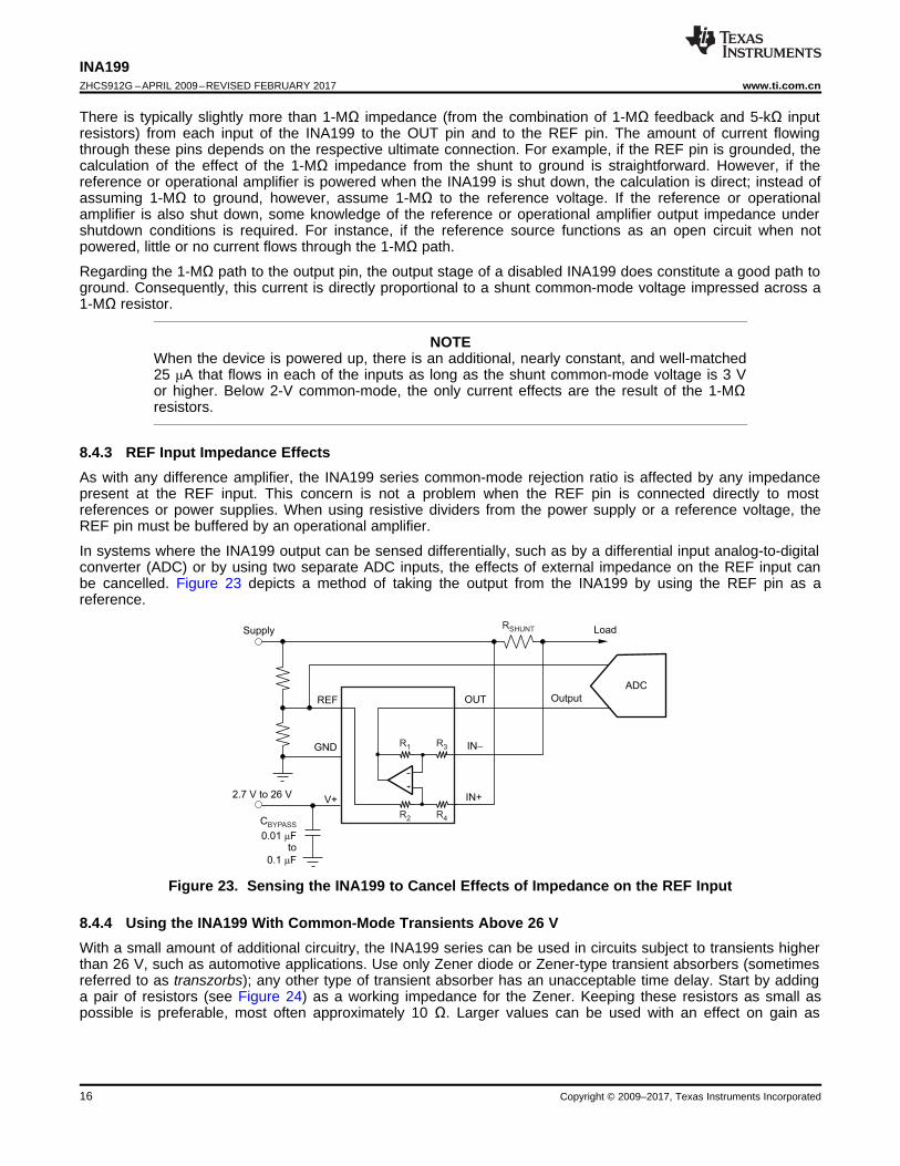
8.4.3 REF Input Impedance EffectsAs with any difference amplifier, the INA199 series common-mode rejection ratio is affected by any impedancepresent at the REF input. This concern is not a problem when the REF pin is connected directly to mostreferences or power supplies. When using resistive dividers from the power supply or a reference voltage, theREF pin must be buffered by an operational amplifier.
In systems where the INA199 output can be sensed differentially, such as by a differential input analog-to-digitalconverter (ADC) or by using two separate ADC inputs, the effects of external impedance on the REF input canbe cancelled. Figure 23 depicts a method of taking the output from the INA199 by using the REF pin as areference.
Figure 23. Sensing the INA199 to Cancel Effects of Impedance on the REF Input
8.4.4 Using the INA199 With Common-Mode Transients Above 26 VWith a small amount of additional circuitry, the INA199 series can be used in circuits subject to transients higherthan 26 V, such as automotive applications. Use only Zener diode or Zener-type transient absorbers (sometimesreferred to as transzorbs); any other type of transient absorber has an unacceptable time delay. Start by addinga pair of resistors (see Figure 24) as a working impedance for the Zener. Keeping these resistors as small aspossible is preferable, most often approximately 10 Ω. Larger values can be used with an effect on gain as

V+
OUT
GND IN-
IN+
CBYPASS
Shutdown
Control
REF
Reference
Voltage
Supply LoadRSHUNT
Output
1 MW
RPROTECT
10 W
RPROTECT
10 W
R3
1 MW R4
V+
OUT
GND IN-
IN+
CBYPASS
Shutdown
Control
REF
Reference
Voltage
Supply LoadRSHUNT
Output
1 MW
RPROTECT
10 W
RPROTECT
10 W
R3
1 MW R4
17
INA199www.ti.com.cn ZHCS912G –APRIL 2009–REVISED FEBRUARY 2017
Copyright © 2009–2017, Texas Instruments Incorporated
discussed in the Input Filtering section. Because this circuit limits only short-term transients, many applicationsare satisfied with a 10-Ω resistor along with conventional Zener diodes of the lowest power rating that can befound. This combination uses the least amount of board space. These diodes can be found in packages as smallas SOT-523 or SOD-523. See TIDA-00302 Transient Robustness for Current Shunt Monitor Design Guide,TIDU473 for more information on transient robustness and current-shunt monitor input protection.
Figure 24. INA199 Transient Protection Using Dual Zener Diodes
In the event that low-power zeners do not have sufficient transient absorption capability and a higher powertranszorb must be used, the most package-efficient solution then involves using a single transzorb and back-to-back diodes between the device inputs. The most space-efficient solutions are dual series-connected diodes in asingle SOT-523 or SOD-523 package. This method is shown in Figure 25. In either of these examples, the totalboard area required by the INA199 with all protective components is less than that of an SO-8 package, and onlyslightly greater than that of an MSOP-8 package.
Figure 25. INA199 Transient Protection Using a Single Transzorb and Input Clamps

OUT
IN+
IN-
-
+
REF
GND
V+
1 MW
1 MW
R3
R42.7 V to 26 V
ReferenceVoltage
Shunt
Load Supply
Output
0.01 F
to 0.1 F
m
m
MMZ1608B601C
0.01 F
to 0.1 F
m
m
Device
Copyright © 2017, Texas Instruments Incorporated
18
INA199ZHCS912G –APRIL 2009–REVISED FEBRUARY 2017 www.ti.com.cn
Copyright © 2009–2017, Texas Instruments Incorporated
8.4.5 Improving Transient RobustnessApplications involving large input transients with excessive dV/dt above 2 kV per microsecond present at thedevice input pins can cause damage to the internal ESD structures on version A devices. This potential damageis a result of the internal latching of the ESD structure to ground when this transient occurs at the input. Withsignificant current available in most current-sensing applications, the large current flowing through the inputtransient-triggered, ground-shorted ESD structure quickly results in damage to the silicon. External filtering canbe used to attenuate the transient signal prior to reaching the inputs to avoid the latching condition. Take care toensure that external series input resistance does not significantly affect gain error accuracy. For accuracypurposes, keep the resistance under 10 Ω if possible. Ferrite beads are recommended for this filter because oftheir inherently low dc ohmic value. Ferrite beads with less than 10 Ω of resistance at dc and over 600 Ω ofresistance at 100 MHz to 200 MHz are recommended. The recommended capacitor values for this filter arebetween 0.01 µF and 0.1 µF to ensure adequate attenuation in the high-frequency region. This protectionscheme is shown in Figure 26. Again, see TIDA-00302 Transient Robustness for Current Shunt Monitor DesignGuide, TIDU473 for more information on transient robustness and current-shunt monitor input protection.
Figure 26. Transient Protection
To minimize the cost of adding these external components to protect the device in applications where largetransient signals may be present, version B and C devices are now available with new ESD structures that arenot susceptible to this latching condition. Version B and C devices are incapable of sustaining these damage-causing latched conditions so these devices do not have the same sensitivity to the transients that the version Adevices have, thus making the version B and C devices a better fit for these applications.

CBYPASS
0.1 µF
Power SupplyLoad
Output-
+
IN-
IN+
GND
V+
OUT
REF
Bus Supply
Copyright © 2017, Texas Instruments Incorporated
19
INA199www.ti.com.cn ZHCS912G –APRIL 2009–REVISED FEBRUARY 2017
Copyright © 2009–2017, Texas Instruments Incorporated
9 Application and Implementation
NOTEInformation in the following applications sections is not part of the TI componentspecification, and TI does not warrant its accuracy or completeness. TI’s customers areresponsible for determining suitability of components for their purposes. Customers shouldvalidate and test their design implementation to confirm system functionality.
9.1 Application InformationThe INA199 measures the voltage developed across a current-sensing resistor when current passes through it.The ability to drive the reference pin to adjust the functionality of the output signal offers multiple configurations,as discussed throughout this section.
9.2 Typical Applications
9.2.1 Unidirectional Operation
Figure 27. Unidirectional Application Schematic
9.2.1.1 Design RequirementsThe device can be configured to monitor current flowing in one direction (unidirectional) or in both directions(bidirectional) depending on how the REF pin is configured. The most common case is unidirectional where theoutput is set to ground when no current is flowing by connecting the REF pin to ground, as shown in Figure 27.When the input signal increases, the output voltage at the OUT pin increases.
9.2.1.2 Detailed Design ProcedureThe linear range of the output stage is limited in how close the output voltage can approach ground under zeroinput conditions. In unidirectional applications where measuring very low input currents is desirable, bias the REFpin to a convenient value above 50 mV to get the output into the linear range of the device. To limit common-mode rejection errors, TI recommends buffering the reference voltage connected to the REF pin.
A less frequently-used output biasing method is to connect the REF pin to the supply voltage, V+. This methodresults in the output voltage saturating at 200 mV below the supply voltage when no differential input signal ispresent. This method is similar to the output saturated low condition with no input signal when the REF pin isconnected to ground. The output voltage in this configuration only responds to negative currents that developnegative differential input voltage relative to the device IN– pin. Under these conditions, when the differentialinput signal increases negatively, the output voltage moves downward from the saturated supply voltage. Thevoltage applied to the REF pin must not exceed the device supply voltage.
--+
Reference Voltage
CBYPASS
0.1 µF
Output-
+
IN-
IN+
GND
V+
OUT
REF
Power SupplyBus Supply Load
Copyright © 2017, Texas Instruments Incorporated
Out
put V
olta
ge
(1 V
/div
)
Time (500 µs /div)
Output
VREF
C001
0V
20
INA199ZHCS912G –APRIL 2009–REVISED FEBRUARY 2017 www.ti.com.cn
Copyright © 2009–2017, Texas Instruments Incorporated
Typical Applications (continued)9.2.1.3 Application CurveAn example output response of a unidirectional configuration is shown in Figure 28. With the REF pin connecteddirectly to ground, the output voltage is biased to this zero output level. The output rises above the referencevoltage for positive differential input signals but cannot fall below the reference voltage for negative differentialinput signals because of the grounded reference voltage.
Figure 28. Unidirectional Application Output Response
9.2.2 Bidirectional Operation
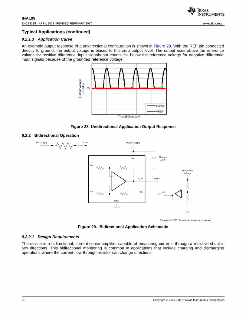
Figure 29. Bidirectional Application Schematic
9.2.2.1 Design RequirementsThe device is a bidirectional, current-sense amplifier capable of measuring currents through a resistive shunt intwo directions. This bidirectional monitoring is common in applications that include charging and dischargingoperations where the current flow-through resistor can change directions.

Out
put V
olta
ge
(1 V
/div
)
Time (500 µs/div)
VOUT VREF
C002
0V
21
INA199www.ti.com.cn ZHCS912G –APRIL 2009–REVISED FEBRUARY 2017
Copyright © 2009–2017, Texas Instruments Incorporated
Typical Applications (continued)9.2.2.2 Detailed Design ProcedureThe ability to measure this current flowing in both directions is enabled by applying a voltage to the REF pin; seeFigure 29. The voltage applied to REF (VREF) sets the output state that corresponds to the zero-input level state.The output then responds by increasing above VREF for positive differential signals (relative to the IN– pin) andresponds by decreasing below VREF for negative differential signals. This reference voltage applied to the REFpin can be set anywhere between 0 V to V+. For bidirectional applications, VREF is typically set at mid-scale forequal signal range in both current directions. In some cases, however, VREF is set at a voltage other than mid-scale when the bidirectional current and corresponding output signal do not need to be symmetrical.
9.2.2.3 Application Curve
Figure 30. Bidirectional Application Output Response

Supply Bypass Capacitor
VIA to Power or Ground Plane
VIA to Ground Plane
Supply Voltage
Output Signal Trace
RE
F
GN
D
V+
IN+IN-
OU
T
Copyright © 2017, Texas Instruments Incorporated
22
INA199ZHCS912G –APRIL 2009–REVISED FEBRUARY 2017 www.ti.com.cn
版权 © 2009–2017, Texas Instruments Incorporated
10 Power Supply RecommendationsThe input circuitry of the INA199 can accurately measure beyond its power-supply voltage, V+. For example, theV+ power supply can be 5 V, whereas the load power-supply voltage can be as high as 26 V. However, theoutput voltage range of the OUT pin is limited by the voltages on the power-supply pin. Also, the INA199 canwithstand the full input signal range up to 26-V range in the input pins, regardless of whether the device haspower applied or not.
11 Layout
11.1 Layout Guidelines• Connect the input pins to the sensing resistor using a kelvin or 4-wire connection. This connection technique
ensures that only the current-sensing resistor impedance is detected between the input pins. Poor routing ofthe current-sensing resistor commonly results in additional resistance present between the input pins. Giventhe very low ohmic value of the current resistor, any additional high-current carrying impedance can causesignificant measurement errors.
• Place the power-supply bypass capacitor as close as possible to the supply and ground pins. TI recommendsusing a bypass capacitor with a value of 0.1 μF. Additional decoupling capacitance can be added tocompensate for noisy or high-impedance power supplies.
11.2 Layout Example
Figure 31. Recommended Layout

23
INA199www.ti.com.cn ZHCS912G –APRIL 2009–REVISED FEBRUARY 2017
版权 © 2009–2017, Texas Instruments Incorporated
12 器器件件和和文文档档支支持持
12.1 文文档档支支持持
12.1.1 相相关关文文档档
相关文档请参阅以下部分:
• 《INA199A1-A3EVM 用户指南》
• 《TIDA-00302 电流分流监控器的瞬态稳定性》
12.2 接接收收文文档档更更新新通通知知
如需接收文档更新通知,请访问 www.ti.com.cn 网站上的器件产品文件夹。点击右上角的提醒我 (Alert me) 注册后,即可每周定期收到已更改的产品信息。有关更改的详细信息,请查阅已修订文档中包含的修订历史记录。
12.3 社社区区资资源源
The following links connect to TI community resources. Linked contents are provided "AS IS" by the respectivecontributors. They do not constitute TI specifications and do not necessarily reflect TI's views; see TI's Terms ofUse.
TI E2E™ Online Community TI's Engineer-to-Engineer (E2E) Community. Created to foster collaborationamong engineers. At e2e.ti.com, you can ask questions, share knowledge, explore ideas and helpsolve problems with fellow engineers.
Design Support TI's Design Support Quickly find helpful E2E forums along with design support tools andcontact information for technical support.
12.4 商商标标
E2E is a trademark of Texas Instruments.All other trademarks are the property of their respective owners.
12.5 静静电电放放电电警警告告ESD 可能会损坏该集成电路。德州仪器 (TI) 建议通过适当的预防措施处理所有集成电路。如果不遵守正确的处理措施和安装程序 , 可能会损坏集成电路。
ESD 的损坏小至导致微小的性能降级 , 大至整个器件故障。 精密的集成电路可能更容易受到损坏 , 这是因为非常细微的参数更改都可能会导致器件与其发布的规格不相符。
12.6 GlossarySLYZ022 — TI Glossary.
This glossary lists and explains terms, acronyms, and definitions.
13 机机械械、、封封装装和和可可订订购购信信息息
以下页中包括机械、封装和可订购信息。这些信息是针对指定器件可提供的最新数据。这些数据会在无通知且不对本文档进行修订的情况下发生改变。欲获得该数据表的浏览器版本,请查阅左侧的导航栏。

PACKAGE OPTION ADDENDUM
www.ti.com 21-Apr-2018
Addendum-Page 1
PACKAGING INFORMATION
Orderable Device Status(1)
Package Type PackageDrawing
Pins PackageQty
Eco Plan(2)
Lead/Ball Finish(6)
MSL Peak Temp(3)
Op Temp (°C) Device Marking(4/5)
Samples
INA199A1DCKR ACTIVE SC70 DCK 6 3000 Green (RoHS& no Sb/Br)
CU NIPDAU Level-2-260C-1 YEAR -40 to 125 OBG
INA199A1DCKT ACTIVE SC70 DCK 6 250 Green (RoHS& no Sb/Br)
CU NIPDAU Level-2-260C-1 YEAR -40 to 125 OBG
INA199A1RSWR ACTIVE UQFN RSW 10 3000 Green (RoHS& no Sb/Br)
CU NIPDAU | Call TI Level-1-260C-UNLIM -40 to 125 NSJ
INA199A1RSWT ACTIVE UQFN RSW 10 250 Green (RoHS& no Sb/Br)
CU NIPDAU | Call TI Level-1-260C-UNLIM -40 to 125 NSJ
INA199A2DCKR ACTIVE SC70 DCK 6 3000 Green (RoHS& no Sb/Br)
CU NIPDAU Level-2-260C-1 YEAR -40 to 125 OBH
INA199A2DCKT ACTIVE SC70 DCK 6 250 Green (RoHS& no Sb/Br)
CU NIPDAU Level-2-260C-1 YEAR -40 to 125 OBH
INA199A2RSWR ACTIVE UQFN RSW 10 3000 Green (RoHS& no Sb/Br)
CU NIPDAU Level-1-260C-UNLIM -40 to 125 NTJ
INA199A2RSWT ACTIVE UQFN RSW 10 250 Green (RoHS& no Sb/Br)
CU NIPDAU Level-1-260C-UNLIM -40 to 125 NTJ
INA199A3DCKR ACTIVE SC70 DCK 6 3000 Green (RoHS& no Sb/Br)
CU NIPDAU Level-2-260C-1 YEAR -40 to 125 OBI
INA199A3DCKT ACTIVE SC70 DCK 6 250 Green (RoHS& no Sb/Br)
CU NIPDAU Level-2-260C-1 YEAR -40 to 125 OBI
INA199A3RSWR ACTIVE UQFN RSW 10 3000 Green (RoHS& no Sb/Br)
CU NIPDAU Level-1-260C-UNLIM -40 to 125 NUJ
INA199A3RSWT ACTIVE UQFN RSW 10 250 Green (RoHS& no Sb/Br)
CU NIPDAU Level-1-260C-UNLIM -40 to 125 NUJ
INA199B1DCKR ACTIVE SC70 DCK 6 3000 Green (RoHS& no Sb/Br)
CU NIPDAU Level-2-260C-1 YEAR -40 to 125 SEB
INA199B1DCKT ACTIVE SC70 DCK 6 250 Green (RoHS& no Sb/Br)
CU NIPDAU Level-2-260C-1 YEAR -40 to 125 SEB
INA199B1RSWR ACTIVE UQFN RSW 10 3000 Green (RoHS& no Sb/Br)
CU NIPDAU Level-1-260C-UNLIM -40 to 125 SHV
INA199B1RSWT ACTIVE UQFN RSW 10 250 Green (RoHS& no Sb/Br)
CU NIPDAU Level-1-260C-UNLIM -40 to 125 SHV
INA199B2DCKR ACTIVE SC70 DCK 6 3000 Green (RoHS& no Sb/Br)
CU NIPDAU Level-2-260C-1 YEAR -40 to 125 SEG

PACKAGE OPTION ADDENDUM
www.ti.com 21-Apr-2018
Addendum-Page 2
Orderable Device Status(1)
Package Type PackageDrawing
Pins PackageQty
Eco Plan(2)
Lead/Ball Finish(6)
MSL Peak Temp(3)
Op Temp (°C) Device Marking(4/5)
Samples
INA199B2DCKT ACTIVE SC70 DCK 6 250 Green (RoHS& no Sb/Br)
CU NIPDAU Level-2-260C-1 YEAR -40 to 125 SEG
INA199B2RSWR ACTIVE UQFN RSW 10 3000 Green (RoHS& no Sb/Br)
CU NIPDAU Level-1-260C-UNLIM -40 to 125 SHW
INA199B2RSWT ACTIVE UQFN RSW 10 250 Green (RoHS& no Sb/Br)
CU NIPDAU Level-1-260C-UNLIM -40 to 125 SHW
INA199B3DCKR ACTIVE SC70 DCK 6 3000 Green (RoHS& no Sb/Br)
CU NIPDAU Level-2-260C-1 YEAR -40 to 125 SHE
INA199B3DCKT ACTIVE SC70 DCK 6 250 Green (RoHS& no Sb/Br)
CU NIPDAU Level-2-260C-1 YEAR -40 to 125 SHE
INA199B3RSWR ACTIVE UQFN RSW 10 3000 Green (RoHS& no Sb/Br)
CU NIPDAU Level-1-260C-UNLIM -40 to 125 SHX
INA199B3RSWT ACTIVE UQFN RSW 10 250 Green (RoHS& no Sb/Br)
CU NIPDAU Level-1-260C-UNLIM -40 to 125 SHX
INA199C1DCKR ACTIVE SC70 DCK 6 3000 Green (RoHS& no Sb/Br)
CU NIPDAU Level-2-260C-1 YEAR -40 to 125 16L
INA199C1DCKT ACTIVE SC70 DCK 6 250 Green (RoHS& no Sb/Br)
CU NIPDAU Level-2-260C-1 YEAR -40 to 125 16L
INA199C1RSWR ACTIVE UQFN RSW 10 3000 Green (RoHS& no Sb/Br)
CU NIPDAU Level-1-260C-UNLIM -40 to 125 16O
INA199C1RSWT ACTIVE UQFN RSW 10 250 Green (RoHS& no Sb/Br)
CU NIPDAU Level-1-260C-UNLIM -40 to 125 16O
INA199C2DCKR ACTIVE SC70 DCK 6 3000 Green (RoHS& no Sb/Br)
CU NIPDAU Level-2-260C-1 YEAR -40 to 125 16M
INA199C2DCKT ACTIVE SC70 DCK 6 250 Green (RoHS& no Sb/Br)
CU NIPDAU Level-2-260C-1 YEAR -40 to 125 16M
INA199C2RSWR ACTIVE UQFN RSW 10 3000 Green (RoHS& no Sb/Br)
CU NIPDAU Level-1-260C-UNLIM -40 to 125 16P
INA199C2RSWT ACTIVE UQFN RSW 10 250 Green (RoHS& no Sb/Br)
CU NIPDAU Level-1-260C-UNLIM -40 to 125 16P
INA199C3DCKR ACTIVE SC70 DCK 6 3000 Green (RoHS& no Sb/Br)
CU NIPDAU Level-2-260C-1 YEAR -40 to 125 16N
INA199C3DCKT ACTIVE SC70 DCK 6 250 Green (RoHS& no Sb/Br)
CU NIPDAU Level-2-260C-1 YEAR -40 to 125 16N
INA199C3RSWR ACTIVE UQFN RSW 10 3000 Green (RoHS& no Sb/Br)
CU NIPDAU Level-1-260C-UNLIM -40 to 125 16Q

PACKAGE OPTION ADDENDUM
www.ti.com 21-Apr-2018
Addendum-Page 3
Orderable Device Status(1)
Package Type PackageDrawing
Pins PackageQty
Eco Plan(2)
Lead/Ball Finish(6)
MSL Peak Temp(3)
Op Temp (°C) Device Marking(4/5)
Samples
INA199C3RSWT ACTIVE UQFN RSW 10 250 Green (RoHS& no Sb/Br)
CU NIPDAU Level-1-260C-UNLIM -40 to 125 16Q
(1) The marketing status values are defined as follows:ACTIVE: Product device recommended for new designs.LIFEBUY: TI has announced that the device will be discontinued, and a lifetime-buy period is in effect.NRND: Not recommended for new designs. Device is in production to support existing customers, but TI does not recommend using this part in a new design.PREVIEW: Device has been announced but is not in production. Samples may or may not be available.OBSOLETE: TI has discontinued the production of the device.
(2) RoHS: TI defines "RoHS" to mean semiconductor products that are compliant with the current EU RoHS requirements for all 10 RoHS substances, including the requirement that RoHS substancedo not exceed 0.1% by weight in homogeneous materials. Where designed to be soldered at high temperatures, "RoHS" products are suitable for use in specified lead-free processes. TI mayreference these types of products as "Pb-Free".RoHS Exempt: TI defines "RoHS Exempt" to mean products that contain lead but are compliant with EU RoHS pursuant to a specific EU RoHS exemption.Green: TI defines "Green" to mean the content of Chlorine (Cl) and Bromine (Br) based flame retardants meet JS709B low halogen requirements of <=1000ppm threshold. Antimony trioxide basedflame retardants must also meet the <=1000ppm threshold requirement.
(3) MSL, Peak Temp. - The Moisture Sensitivity Level rating according to the JEDEC industry standard classifications, and peak solder temperature.
(4) There may be additional marking, which relates to the logo, the lot trace code information, or the environmental category on the device.
(5) Multiple Device Markings will be inside parentheses. Only one Device Marking contained in parentheses and separated by a "~" will appear on a device. If a line is indented then it is a continuationof the previous line and the two combined represent the entire Device Marking for that device.
(6) Lead/Ball Finish - Orderable Devices may have multiple material finish options. Finish options are separated by a vertical ruled line. Lead/Ball Finish values may wrap to two lines if the finishvalue exceeds the maximum column width.
Important Information and Disclaimer:The information provided on this page represents TI's knowledge and belief as of the date that it is provided. TI bases its knowledge and belief on informationprovided by third parties, and makes no representation or warranty as to the accuracy of such information. Efforts are underway to better integrate information from third parties. TI has taken andcontinues to take reasonable steps to provide representative and accurate information but may not have conducted destructive testing or chemical analysis on incoming materials and chemicals.TI and TI suppliers consider certain information to be proprietary, and thus CAS numbers and other limited information may not be available for release.
In no event shall TI's liability arising out of such information exceed the total purchase price of the TI part(s) at issue in this document sold by TI to Customer on an annual basis.

TAPE AND REEL INFORMATION
*All dimensions are nominal
Device PackageType
PackageDrawing
Pins SPQ ReelDiameter
(mm)
ReelWidth
W1 (mm)
A0(mm)
B0(mm)
K0(mm)
P1(mm)
W(mm)
Pin1Quadrant
INA199A1DCKR SC70 DCK 6 3000 179.0 8.4 2.2 2.5 1.2 4.0 8.0 Q3
INA199A1DCKR SC70 DCK 6 3000 178.0 9.0 2.4 2.5 1.2 4.0 8.0 Q3
INA199A1DCKR SC70 DCK 6 3000 180.0 8.4 2.41 2.41 1.2 4.0 8.0 Q3
INA199A1DCKT SC70 DCK 6 250 178.0 9.0 2.4 2.5 1.2 4.0 8.0 Q3
INA199A1DCKT SC70 DCK 6 250 179.0 8.4 2.2 2.5 1.2 4.0 8.0 Q3
INA199A1RSWR UQFN RSW 10 3000 179.0 8.4 1.7 2.1 0.7 4.0 8.0 Q1
INA199A1RSWT UQFN RSW 10 250 179.0 8.4 1.7 2.1 0.7 4.0 8.0 Q1
INA199A2DCKR SC70 DCK 6 3000 178.0 9.0 2.4 2.5 1.2 4.0 8.0 Q3
INA199A2DCKR SC70 DCK 6 3000 179.0 8.4 2.2 2.5 1.2 4.0 8.0 Q3
INA199A2DCKR SC70 DCK 6 3000 180.0 8.4 2.47 2.3 1.25 4.0 8.0 Q3
INA199A2DCKT SC70 DCK 6 250 180.0 8.4 2.47 2.3 1.25 4.0 8.0 Q3
INA199A2DCKT SC70 DCK 6 250 178.0 9.0 2.4 2.5 1.2 4.0 8.0 Q3
INA199A2DCKT SC70 DCK 6 250 179.0 8.4 2.2 2.5 1.2 4.0 8.0 Q3
INA199A2RSWR UQFN RSW 10 3000 179.0 8.4 1.7 2.1 0.7 4.0 8.0 Q1
INA199A2RSWT UQFN RSW 10 250 179.0 8.4 1.7 2.1 0.7 4.0 8.0 Q1
INA199A3DCKR SC70 DCK 6 3000 178.0 9.0 2.4 2.5 1.2 4.0 8.0 Q3
INA199A3DCKR SC70 DCK 6 3000 179.0 8.4 2.2 2.5 1.2 4.0 8.0 Q3
INA199A3DCKT SC70 DCK 6 250 179.0 8.4 2.2 2.5 1.2 4.0 8.0 Q3
PACKAGE MATERIALS INFORMATION
www.ti.com 8-Aug-2018
Pack Materials-Page 1

Device PackageType
PackageDrawing
Pins SPQ ReelDiameter
(mm)
ReelWidth
W1 (mm)
A0(mm)
B0(mm)
K0(mm)
P1(mm)
W(mm)
Pin1Quadrant
INA199A3DCKT SC70 DCK 6 250 178.0 9.0 2.4 2.5 1.2 4.0 8.0 Q3
INA199A3RSWR UQFN RSW 10 3000 179.0 8.4 1.7 2.1 0.7 4.0 8.0 Q1
INA199A3RSWT UQFN RSW 10 250 179.0 8.4 1.7 2.1 0.7 4.0 8.0 Q1
INA199B1DCKR SC70 DCK 6 1 178.0 9.0 2.4 2.5 1.2 4.0 8.0 Q3
INA199B1DCKT SC70 DCK 6 250 178.0 9.0 2.4 2.5 1.2 4.0 8.0 Q3
INA199B1RSWR UQFN RSW 10 3000 179.0 8.4 1.7 2.1 0.7 4.0 8.0 Q1
INA199B1RSWT UQFN RSW 10 250 179.0 8.4 1.7 2.1 0.7 4.0 8.0 Q1
INA199B2DCKR SC70 DCK 6 3000 178.0 9.0 2.4 2.5 1.2 4.0 8.0 Q3
INA199B2DCKT SC70 DCK 6 250 178.0 9.0 2.4 2.5 1.2 4.0 8.0 Q3
INA199B2RSWR UQFN RSW 10 3000 179.0 8.4 1.7 2.1 0.7 4.0 8.0 Q1
INA199B2RSWT UQFN RSW 10 250 179.0 8.4 1.7 2.1 0.7 4.0 8.0 Q1
INA199B3DCKR SC70 DCK 6 3000 178.0 9.0 2.4 2.5 1.2 4.0 8.0 Q3
INA199B3DCKT SC70 DCK 6 250 178.0 9.0 2.4 2.5 1.2 4.0 8.0 Q3
INA199B3RSWR UQFN RSW 10 3000 179.0 8.4 1.7 2.1 0.7 4.0 8.0 Q1
INA199B3RSWT UQFN RSW 10 250 179.0 8.4 1.7 2.1 0.7 4.0 8.0 Q1
INA199C1DCKR SC70 DCK 6 3000 178.0 9.0 2.4 2.5 1.2 4.0 8.0 Q3
INA199C1DCKT SC70 DCK 6 250 178.0 8.4 2.4 2.5 1.2 4.0 8.0 Q3
INA199C1RSWR UQFN RSW 10 3000 179.0 8.4 1.7 2.1 0.7 4.0 8.0 Q1
INA199C1RSWT UQFN RSW 10 250 179.0 8.4 1.7 2.1 0.7 4.0 8.0 Q1
INA199C2DCKR SC70 DCK 6 3000 178.0 9.0 2.4 2.5 1.2 4.0 8.0 Q3
INA199C2DCKT SC70 DCK 6 250 178.0 8.4 2.4 2.5 1.2 4.0 8.0 Q3
INA199C2RSWR UQFN RSW 10 3000 179.0 8.4 1.7 2.1 0.7 4.0 8.0 Q1
INA199C2RSWT UQFN RSW 10 250 179.0 8.4 1.7 2.1 0.7 4.0 8.0 Q1
INA199C3DCKR SC70 DCK 6 3000 178.0 9.0 2.4 2.5 1.2 4.0 8.0 Q3
INA199C3DCKT SC70 DCK 6 250 178.0 8.4 2.4 2.5 1.2 4.0 8.0 Q3
INA199C3RSWR UQFN RSW 10 3000 179.0 8.4 1.7 2.1 0.7 4.0 8.0 Q1
INA199C3RSWT UQFN RSW 10 250 179.0 8.4 1.7 2.1 0.7 4.0 8.0 Q1
PACKAGE MATERIALS INFORMATION
www.ti.com 8-Aug-2018
Pack Materials-Page 2

*All dimensions are nominal
Device Package Type Package Drawing Pins SPQ Length (mm) Width (mm) Height (mm)
INA199A1DCKR SC70 DCK 6 3000 195.0 200.0 45.0
INA199A1DCKR SC70 DCK 6 3000 180.0 180.0 18.0
INA199A1DCKR SC70 DCK 6 3000 202.0 201.0 28.0
INA199A1DCKT SC70 DCK 6 250 180.0 180.0 18.0
INA199A1DCKT SC70 DCK 6 250 195.0 200.0 45.0
INA199A1RSWR UQFN RSW 10 3000 203.0 203.0 35.0
INA199A1RSWT UQFN RSW 10 250 203.0 203.0 35.0
INA199A2DCKR SC70 DCK 6 3000 180.0 180.0 18.0
INA199A2DCKR SC70 DCK 6 3000 195.0 200.0 45.0
INA199A2DCKR SC70 DCK 6 3000 223.0 270.0 35.0
INA199A2DCKT SC70 DCK 6 250 223.0 270.0 35.0
INA199A2DCKT SC70 DCK 6 250 180.0 180.0 18.0
INA199A2DCKT SC70 DCK 6 250 195.0 200.0 45.0
INA199A2RSWR UQFN RSW 10 3000 203.0 203.0 35.0
INA199A2RSWT UQFN RSW 10 250 203.0 203.0 35.0
INA199A3DCKR SC70 DCK 6 3000 180.0 180.0 18.0
INA199A3DCKR SC70 DCK 6 3000 195.0 200.0 45.0
INA199A3DCKT SC70 DCK 6 250 195.0 200.0 45.0
INA199A3DCKT SC70 DCK 6 250 180.0 180.0 18.0
INA199A3RSWR UQFN RSW 10 3000 203.0 203.0 35.0
PACKAGE MATERIALS INFORMATION
www.ti.com 8-Aug-2018
Pack Materials-Page 3

Device Package Type Package Drawing Pins SPQ Length (mm) Width (mm) Height (mm)
INA199A3RSWT UQFN RSW 10 250 203.0 203.0 35.0
INA199B1DCKR SC70 DCK 6 1 180.0 180.0 18.0
INA199B1DCKT SC70 DCK 6 250 180.0 180.0 18.0
INA199B1RSWR UQFN RSW 10 3000 203.0 203.0 35.0
INA199B1RSWT UQFN RSW 10 250 203.0 203.0 35.0
INA199B2DCKR SC70 DCK 6 3000 180.0 180.0 18.0
INA199B2DCKT SC70 DCK 6 250 180.0 180.0 18.0
INA199B2RSWR UQFN RSW 10 3000 203.0 203.0 35.0
INA199B2RSWT UQFN RSW 10 250 203.0 203.0 35.0
INA199B3DCKR SC70 DCK 6 3000 180.0 180.0 18.0
INA199B3DCKT SC70 DCK 6 250 180.0 180.0 18.0
INA199B3RSWR UQFN RSW 10 3000 203.0 203.0 35.0
INA199B3RSWT UQFN RSW 10 250 203.0 203.0 35.0
INA199C1DCKR SC70 DCK 6 3000 340.0 340.0 38.0
INA199C1DCKT SC70 DCK 6 250 340.0 340.0 38.0
INA199C1RSWR UQFN RSW 10 3000 203.0 203.0 35.0
INA199C1RSWT UQFN RSW 10 250 203.0 203.0 35.0
INA199C2DCKR SC70 DCK 6 3000 180.0 180.0 18.0
INA199C2DCKT SC70 DCK 6 250 340.0 340.0 38.0
INA199C2RSWR UQFN RSW 10 3000 203.0 203.0 35.0
INA199C2RSWT UQFN RSW 10 250 203.0 203.0 35.0
INA199C3DCKR SC70 DCK 6 3000 180.0 180.0 18.0
INA199C3DCKT SC70 DCK 6 250 180.0 180.0 18.0
INA199C3RSWR UQFN RSW 10 3000 203.0 203.0 35.0
INA199C3RSWT UQFN RSW 10 250 203.0 203.0 35.0
PACKAGE MATERIALS INFORMATION
www.ti.com 8-Aug-2018
Pack Materials-Page 4


重重要要声声明明
德州仪器 (TI) 公司有权按照最新发布的 JESD46 对其半导体产品和服务进行纠正、增强、改进和其他修改,并不再按最新发布的 JESD48 提供任何产品和服务。买方在下订单前应获取最新的相关信息,并验证这些信息是否完整且是最新的。
TI 公布的半导体产品销售条款 (http://www.ti.com/sc/docs/stdterms.htm) 适用于 TI 已认证和批准上市的已封装集成电路产品的销售。另有其他条款可能适用于其他类型 TI 产品及服务的使用或销售。
复制 TI 数据表上 TI 信息的重要部分时,不得变更该等信息,且必须随附所有相关保证、条件、限制和通知,否则不得复制。TI 对该等复制文件不承担任何责任。第三方信息可能受到其它限制条件的制约。在转售 TI 产品或服务时,如果存在对产品或服务参数的虚假陈述,则会失去相关 TI 产品或服务的明示或暗示保证,且构成不公平的、欺诈性商业行为。TI 对此类虚假陈述不承担任何责任。
买方和在系统中整合 TI 产品的其他开发人员(总称“设计人员”)理解并同意,设计人员在设计应用时应自行实施独立的分析、评价和判断,且应全权 负责并确保 应用的安全性, 及设计人员的 应用 (包括应用中使用的所有 TI 产品)应符合所有适用的法律法规及其他相关要求。设计人员就自己设计的 应用声明,其具备制订和实施下列保障措施所需的一切必要专业知识,能够 (1) 预见故障的危险后果,(2) 监视故障及其后果,以及 (3) 降低可能导致危险的故障几率并采取适当措施。设计人员同意,在使用或分发包含 TI 产品的任何 应用前, 将彻底测试该等 应用和 和该等应用所用 TI 产品的 功能而设计。
TI 提供技术、应用或其他设计建议、质量特点、可靠性数据或其他服务或信息,包括但不限于与评估模块有关的参考设计和材料(总称“TI 资源”),旨在帮助设计人员开发整合了 TI 产品的 应用, 如果设计人员(个人,或如果是代表公司,则为设计人员的公司)以任何方式下载、访问或使用任何特定的 TI 资源,即表示其同意仅为该等目标,按照本通知的条款使用任何特定 TI 资源。
TI 所提供的 TI 资源,并未扩大或以其他方式修改 TI 对 TI 产品的公开适用的质保及质保免责声明;也未导致 TI 承担任何额外的义务或责任。TI 有权对其 TI 资源进行纠正、增强、改进和其他修改。除特定 TI 资源的公开文档中明确列出的测试外,TI 未进行任何其他测试。
设计人员只有在开发包含该等 TI 资源所列 TI 产品的 应用时, 才被授权使用、复制和修改任何相关单项 TI 资源。但并未依据禁止反言原则或其他法理授予您任何TI知识产权的任何其他明示或默示的许可,也未授予您 TI 或第三方的任何技术或知识产权的许可,该等产权包括但不限于任何专利权、版权、屏蔽作品权或与使用TI产品或服务的任何整合、机器制作、流程相关的其他知识产权。涉及或参考了第三方产品或服务的信息不构成使用此类产品或服务的许可或与其相关的保证或认可。使用 TI 资源可能需要您向第三方获得对该等第三方专利或其他知识产权的许可。
TI 资源系“按原样”提供。TI 兹免除对资源及其使用作出所有其他明确或默认的保证或陈述,包括但不限于对准确性或完整性、产权保证、无屡发故障保证,以及适销性、适合特定用途和不侵犯任何第三方知识产权的任何默认保证。TI 不负责任何申索,包括但不限于因组合产品所致或与之有关的申索,也不为或对设计人员进行辩护或赔偿,即使该等产品组合已列于 TI 资源或其他地方。对因 TI 资源或其使用引起或与之有关的任何实际的、直接的、特殊的、附带的、间接的、惩罚性的、偶发的、从属或惩戒性损害赔偿,不管 TI 是否获悉可能会产生上述损害赔偿,TI 概不负责。
除 TI 已明确指出特定产品已达到特定行业标准(例如 ISO/TS 16949 和 ISO 26262)的要求外,TI 不对未达到任何该等行业标准要求而承担任何责任。
如果 TI 明确宣称产品有助于功能安全或符合行业功能安全标准,则该等产品旨在帮助客户设计和创作自己的 符合 相关功能安全标准和要求的应用。在应用内使用产品的行为本身不会 配有 任何安全特性。设计人员必须确保遵守适用于其应用的相关安全要求和 标准而设计。设计人员不可将任何 TI 产品用于关乎性命的医疗设备,除非已由各方获得授权的管理人员签署专门的合同对此类应用专门作出规定。关乎性命的医疗设备是指出现故障会导致严重身体伤害或死亡的医疗设备(例如生命保障设备、心脏起搏器、心脏除颤器、人工心脏泵、神经刺激器以及植入设备)。此类设备包括但不限于,美国食品药品监督管理局认定为 III 类设备的设备,以及在美国以外的其他国家或地区认定为同等类别设备的所有医疗设备。
TI 可能明确指定某些产品具备某些特定资格(例如 Q100、军用级或增强型产品)。设计人员同意,其具备一切必要专业知识,可以为自己的应用选择适合的 产品, 并且正确选择产品的风险由设计人员承担。设计人员单方面负责遵守与该等选择有关的所有法律或监管要求。
设计人员同意向 TI 及其代表全额赔偿因其不遵守本通知条款和条件而引起的任何损害、费用、损失和/或责任。IMPORTANT NOTICE
邮寄地址:上海市浦东新区世纪大道 1568 号中建大厦 32 楼,邮政编码:200122Copyright © 2018 德州仪器半导体技术(上海)有限公司