Embed Size (px)
Citation preview
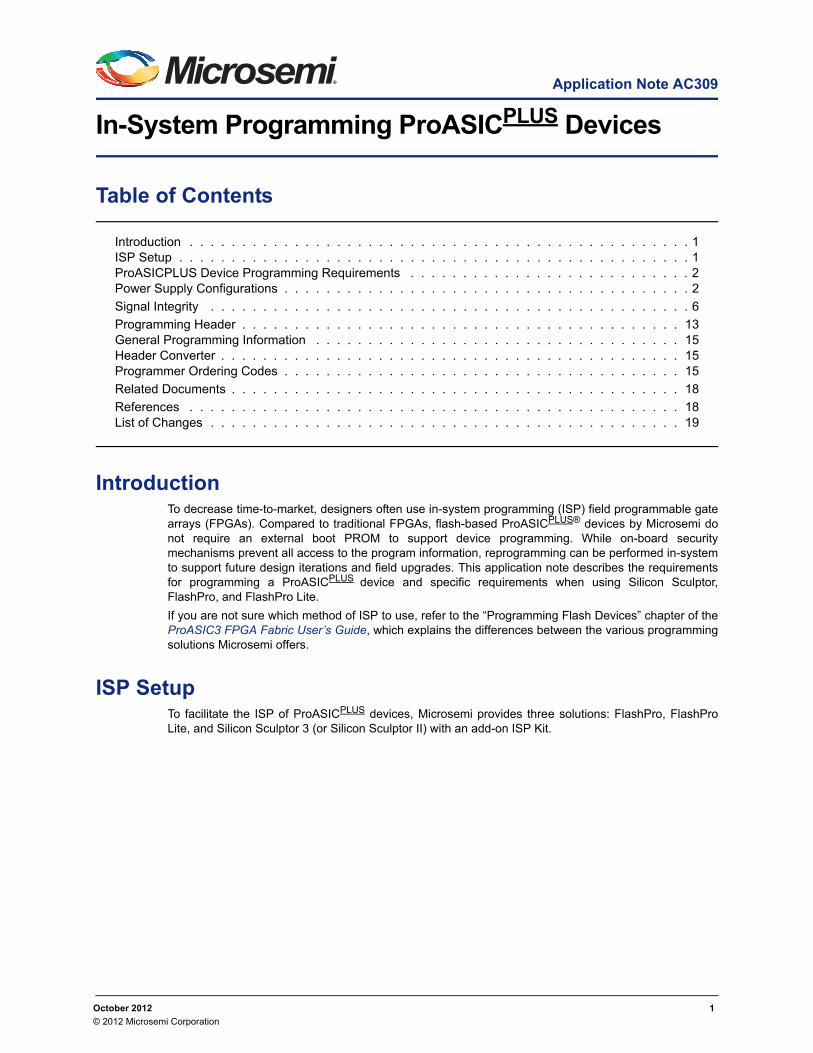
Application Note AC309
In-System Programming ProASICPLUS Devices
Table of Contents
IntroductionTo decrease time-to-market, designers often use in-system programming (ISP) field programmable gatearrays (FPGAs). Compared to traditional FPGAs, flash-based ProASICPLUS® devices by Microsemi donot require an external boot PROM to support device programming. While on-board securitymechanisms prevent all access to the program information, reprogramming can be performed in-systemto support future design iterations and field upgrades. This application note describes the requirementsfor programming a ProASICPLUS device and specific requirements when using Silicon Sculptor,FlashPro, and FlashPro Lite.
If you are not sure which method of ISP to use, refer to the “Programming Flash Devices” chapter of theProASIC3 FPGA Fabric User’s Guide, which explains the differences between the various programmingsolutions Microsemi offers.
ISP SetupTo facilitate the ISP of ProASICPLUS devices, Microsemi provides three solutions: FlashPro, FlashProLite, and Silicon Sculptor 3 (or Silicon Sculptor II) with an add-on ISP Kit.
Introduction . . . . . . . . . . . . . . . . . . . . . . . . . . . . . . . . . . . . . . . . . . . . . . . . 1ISP Setup . . . . . . . . . . . . . . . . . . . . . . . . . . . . . . . . . . . . . . . . . . . . . . . . . 1ProASICPLUS Device Programming Requirements . . . . . . . . . . . . . . . . . . . . . . . . . . . 2Power Supply Configurations . . . . . . . . . . . . . . . . . . . . . . . . . . . . . . . . . . . . . . . 2
Signal Integrity . . . . . . . . . . . . . . . . . . . . . . . . . . . . . . . . . . . . . . . . . . . . . . 6
Programming Header . . . . . . . . . . . . . . . . . . . . . . . . . . . . . . . . . . . . . . . . . . 13General Programming Information . . . . . . . . . . . . . . . . . . . . . . . . . . . . . . . . . . . 15Header Converter . . . . . . . . . . . . . . . . . . . . . . . . . . . . . . . . . . . . . . . . . . . . 15Programmer Ordering Codes . . . . . . . . . . . . . . . . . . . . . . . . . . . . . . . . . . . . . . 15
Related Documents . . . . . . . . . . . . . . . . . . . . . . . . . . . . . . . . . . . . . . . . . . . 18
References . . . . . . . . . . . . . . . . . . . . . . . . . . . . . . . . . . . . . . . . . . . . . . . 18List of Changes . . . . . . . . . . . . . . . . . . . . . . . . . . . . . . . . . . . . . . . . . . . . . 19
October 2012 1
© 2012 Microsemi Corporation

In-System Programming ProASICPLUS Devices
Figure 1 shows the programming setup with FlashPro and Silicon Sculptor.
ProASICPLUS Device Programming RequirementsDuring programming, all I/O pins, except for JTAG interface pins, are tristated and pulled up to VDDP.This isolates the part and prevents the signals from floating.
Interruptions in the programming sequence may result in unpredictable behavior of a partiallyprogrammed device. Additionally, switches that are programmed incorrectly can cause high current flowthrough the circuitry, resulting in permanent damage to the device.
Power Supply ConfigurationsTwo power supplies, one for the VDD pins and the other for the VDDP pins, are needed in normaloperation. VDD powers the core and VDDP powers the input/output (I/O) pads. VDD must be set to 2.5 V(±0.2 V), and VDDP can be set to either 2.5 V (±0.2 V) or 3.3 V (±0.3 V) (Table 1).
During programming for ProASICPLUS devices, VDDP supplies power to the JTAG I/Os and VDDsupplies power to the programming circuit. In addition to the low voltage power supplies (VDD andVDDP), two high voltage sources (VPP and VPN) are necessary (Table 1).
FlashProIf FlashPro is used for programming, all programming voltages (VDD, VDDP, VPP, and VPN) can beprovided by FlashPro. However, the VDD and VDDP supplies of ProASICPLUS devices can be providedfrom the target, while the VPP and VPN are still supplied by FlashPro. Corresponding FlashPro softwareconfiguration is needed to uncheck the VDD and VDDP supply from FlashPro.
FlashPro LiteIf FlashPro Lite is used for programming, the programmer derives all of its power from the target board'sVDD supply. The FlashPro Lite's VPP and VPN power supplies use the target board's VDD as a powersource. The target board must supply power to both the VDDP and VDD power pins of the ProASICPLUS
device in addition to supplying VDD to the FlashPro Lite. The target board needs to provide at least 500 mA of current to the FlashPro Lite VDD connection for programming.
Figure 1 • Programming Setup
2

Power Supply Configurations
Silicon Sculptor 3 and Silicon Sculptor IIIf Silicon Sculptor 3 / Silicon Sculptor II is used for programming, the programmer is providing all thepower supplies. However, you can also choose to power up the VDD and VDDP supplies of theProASICPLUS devices from the target, if you disconnect the VDD and VDDP supplies from the SiliconSculptor 3 / Silicon Sculptor II.
The typical current consumption for each programming pin during programming is shown in Table 1.
Board Considerations
ProASICPLUS Devices – APA450, APA600, APA750, APA1000Microsemi requires bypass capacitors from VPP to GND and VPN to GND for APA450, APA600,APA750, and APA1000 devices during programming. During the erase cycle, ProASICPLUS devices mayhave current surges on the VPP and VPN power supplies. The only way to maintain the integrity of thepower distribution to the ProASICPLUS device during these current surges is to counteract the inductanceof the finite length conductors that distribute the power to the device. This can be accomplished byproviding sufficient bypass capacitance between the VPP and VPN pins and GND (using the shortestpaths possible). Without sufficient bypass capacitance to counteract the inductance, the VPP and VPNpins may incur a voltage spike beyond the voltage that the device can withstand.
Use a 0.01 µF to 0.1 µF ceramic capacitor with a 25 V or greater rating. To filter low-frequency noise(decoupling), use a 4.7 µF (low ESR, <1 , tantalum, 25 V or greater rating) capacitor. The capacitorsshould be located as close to the device pins as possible (within 2.5 cm is desirable). The smaller, high-frequency capacitor should be placed closer to the device pins than the larger low-frequencycapacitor. The same dual capacitor circuit should be used on both the VPP and VPN pins (Figure 2).
Pay close attention to the polarity of the tantalum caps when laying out the board. The positive shouldconnect to ground for VPN.
Table 1 • ProASICPLUS Voltages and Currents
Power Supply Normal Operation Programming Mode Current During Programming
VDD 2.5 V 2.3 V to 2.7 V IVDD < 20 mA at VDD
VDDP 2.5 V or 3.3 V1 2.3 V to 2.7 V or 3.0 V to 3.6 V IVDDP < 20 mA at VDDP
VPP 0 V to 16.5 V or floating2 15.8 V to 16.5 V IVPP < 35 mA at VPP
VPN –13.8 V to 0 V or floating3 –13.8 V to –13.2 V IVPN < 15 mA at VPN
Notes:
1. Stresses beyond the maximum voltages listed in the table may cause permanent damage to the device. Devices shouldnot be operated outside of the Recommended Operating Conditions. Refer to the ProASICPLUS Flash Family FPGAsdatasheet.
2. There is a nominal 40 k pull-up resistor on VPP.3. There is a nominal 40 k pull-down resistor on VPN.4. Absolute maximum rating on VPN is 0.5 V. Stresses beyond this limit may damage the device.
3

In-System Programming ProASICPLUS Devices
Notes:
1. For information on the 0 resistor, refer to the “Programmer Specific Requirements” section on page 5 for details.2. For FlashPro and FlashPro Lite, use TCK, and for Silicon Sculptor use both RCK and TCK.3. This is the output of the programmer. This diagram shows the signals that the programmer will drive onto the header in
programming mode.4. This is the pinout of the programming header on the printed circuit board (PCB). The signals that appear on the header
must be connected to the ProASICPLUS device.5. The SENSE pin is connected to the GND on the target board and is used to indicate to the FlashPro or FlashPro Lite
programmer that the cable is correctly connected to the target board.
Figure 2 • ProASIC PLUS ISP Board Layout and Programming Connector Top View
NC
NC
NC
NC
NC
NC
NC
NC
GND
GND
GND
GND
GND
VDDP
VDDP
VDD
VDD
VDD VDD
VDD
VPP
VPN
VDDP VDDP
VDDP
VPP VPP
VPN VPN
SENSE
TCK
TDI
TDO
TMS
RCK
TRST
o
o
o
ooooooooo
o
o
o
o
ooooooooo
o
NC
NC
NC
NC
NC
NC
NC
NC
GND
GND
GND
GND
GND
SENSE
TCK
TDI
TDO
TMS
RCK
TRST
o
o
ooooooooo
o
o
o
o
ooooooooo
o
GND
TCK
TDI
TDO
TMS
RCK
TRST
ZERO
ZERO
3
5
2
VDDP from Target
VDD from Target
PolarizingNotch
Programming HeaderTop View4
Programming Cable ConnectorTop View3
1
3
5
2
4
25
24
26
23
21
ProASICPLUS
Device
R11
R21
+4.7 mF +4.7 mF 0.1 mFor
0.01 mF
0.1 mFor
0.01 mF+
All GND pins from the programmingcable need to be individually connectedto GND on the target board for correct operation.
4

Power Supply Configurations
ProASICPLUS Devices – APA075, APA150, APA300These devices do not require bypass capacitors on the VPP and VPN pins as long as the total combineddistance of the programming cable and the trace length on the board for each pin is less than or equal to18 inches.
For trace lengths greater than 18 inches, use the bypass capacitor recommendations in the previoussection.
Programmer Specific Requirements
FlashPro • Programming Clock signal—Only TCK is used.
• Programming file—Only STAPL files are supported.
• Daisy Chain—Supported.
• To bypass non-Microsemi devices, you need to create chain specific STAPL files usingChainBuilder. For more information on ChainBuilder, refer to the ChainBuilder User’s Guide.
• Power Supply
– Solution 1: The 0 resistor links, R1 and R2 in Figure 2 on page 4, should be populated if theprogrammer is providing the VDD and VDDP supplies. Or they can be replaced by wires onthe PCB to meet easy layout and low cost requirements. Ensure the VDD and VDDP suppliesfrom the target can handle the power supply from the programmer, otherwise use solution 2.
– Solution 2: The 0 resistors, R1 and R2 in Figure 2 on page 4, are optional if the target isproviding the VDD and VDDP supplies. Uncheck the VDD and VDDP supplies from FlashProin the software.
FlashPro Lite • Programming clock signal—Only TCK is used.
• Programming file—Only STAPL files are supported.
• Daisy Chain—Supported. FlashPro Lite will get the bypass devices information from the“device.db” file. You can manually edit the “device.db” file to add in more devices that are not inthe original device list. For more details, contact Microsemi Tech Support.
• Power Supply
FlashPro Lite derives power from target VDD supply.The0 resistor, R2 in Figure 2 on page 4, shouldalways be populated or it can be replaced by the wire on the printed circuit board (PCB) to meet easylayout and low-cost concern. The 0 resistor, R1 in Figure 2 on page 4, is optional at any time or youcan cut off the trace from the target VDDP supply to the programming header VDDP pin.
Silicon Sculptor 3 / Silicon Sculptor II • Programming clock signal—Both RCK and TCK are used.
• Programming file—Both BIT and STAPL files are supported.
• Daisy Chain—Only supports chains of ProASIC or ProASICPLUS devices. Refer to ProASICDaisy-Chain Programming for similar applications.
• Power Supply
– Solution 1: The 0 resistor links, R1 and R2 in Figure 2 on page 4, should be populated if theprogrammer is providing the VDD and VDDP supplies, or they can be replaced by wires onthe PCB to meet easy layout and low cost requirements. Ensure the VDD and VDDP suppliesfrom the target can handle the power supply from the programmer, otherwise use solution 2.
– Solution 2: The 0 resistor links, R1 and R2 in Figure 2 on page 4, should not be populated ifthe target is providing the VDD and VDDP supplies.
5

In-System Programming ProASICPLUS Devices
Signal IntegrityThis section describes signal integrity in relation to the ISP of Microsemi ProASICPLUS devices andanswers some common questions.
Importance of Signal IntegrityWithout reasonably clean signals on the JTAG nets, reliable communication with the parts is not possible.The result of bad signal quality is programming failures with good parts, or in extreme cases, an inabilityto communicate with the part at all. It is even possible to cause physical damage to the ProASICPLUS
device due to an electrical overstress of the tunnel oxide during programming and erasing of the part.
The JTAG specification defines a state machine, the test access port (TAP) controller, which controlscommunication over the JTAG bus. There are two TAP controllers when talking to a JTAG slave, theJTAG controller and the JTAG slave. These two controllers must dance in lock-step for communication totake place. If the slave gets out of step, communication to the slave is lost until the two controllers aresynchronized again. In the case of device programming, the JTAG controller resides in the programmerand the programming software. The JTAG slave is a hardware state machine in the ProASICPLUS device.Transitions between the different TAP states are controlled by the JTAG TMS signal, as it is clocked intothe device by the JTAG clock TCK. The communication is serial so any dropped bits result in failed statetransitions.
Effect of Reflections and CrosstalkReflections will occur during the rise time of TCK or RCK and cause the part to see two clock edgesinstead of one. When this occurs during a data transfer, it corrupts the data.
Effect of Ground BounceGround bounce changes the voltage on the input buffers. This changes the threshold voltage of thesebuffers, since LVCMOS has a threshold voltage of half of the supply voltage. The ground bounce alsoadds a DC offset to the threshold voltage. The end result is that it raises the threshold voltage.
What Happens if TCK Gets Double-Clocked?All of the I/O buffers in the ProASICPLUS devices are built with the same logic macro so the JTAG signalshave the same performance as the rest of the device. The ProASICPLUS device datasheet specifies thatthe device is capable of 150 MHz system performance and up to 250 MHz internal performance. Themaximum clock frequency is listed as 180 MHz. A 180 MHz clock has a period of just 5.6 ns. The clock istypically high for only half of the period or 2.8 ns. Therefore, the ProASICPLUS inputs are capable ofresponding to clock pulses that are 2.8 ns wide even though the programmer is only clocking the JTAGbus at 4 MHz (FlashPro TCK rate). This means that reflections or glitches that are only 2.8 ns wide willstill be seen by the device's TAP controller. If the slave controller sees a 2.8 ns clock glitch when it is notin a stable state, then the glitch will affect the programming.
The stable states for the TAP controller are: Test-Logic-Reset, Run-Test/Idle, Pause-DR, and Pause-IR.All other states of the TAP controller will have a negative side effect from a clock glitch, either the statewill change or extra repeated data bits will be clocked into the part.
What Happens if RCK Gets Double-Clocked?An occasional double clocking of RCK is not as severe as double clocking for TCK. Since RCK is usedfor timing programming pulses, an occasional double clock just shortens the programming pulse width.Since all flash switches do not take the same amount of time to program, there is a marginal amount ofover-programming that occurs for most switches. In most cases, an infrequent double clocking of RCKwill reduce the over-programming, but not cause a failure. A continuous double clocking could cut all ofthe programming pulses in half and this could have noticeable results. Cutting the programming pulseramp rates can cause electrical over-stress to the tunnel oxide and cause permanent damage to thedevice.
6

Signal Integrity
What is RCK and Why is it Needed for Internal ISP? The ProASICPLUS device contains an internal programming controller that controls the programming ofthe flash switches. Voltages used during programming are based on an internal voltage reference, butthe controller needs a 1 MHz clock derived from either RCK or TCK as its time reference. The partincludes an internal five-bit programmable clock divider, so the external clock can be any multiple of 1 MHz, between 1 MHz and 31 MHz. The external time reference can either come from TCK or RCK.The RCK input is provided as an easy to use reference clock input. Connect an appropriate oscillator tothe RCK pin and the programming controller's clock reference needs are met.
Silicon Sculptor uses the RCK input during programming because its TCK clock is under control of aprogram running on an internal microprocessor. Because it uses RCK, Silicon Sculptor only needs tosend a TCK when it wants to communicate over the JTAG bus. If TCK is set at a constant frequency thatis an integral multiple of 1 MHz and never stopped during programming, then it can be used as thereference clock instead of RCK.
The FlashPro and FlashPro Lite programmers use TCK as the reference clock so it does not need anRCK. The trade-off is that FlashPro or FlashPro Lite needs to have a hardware state controller that willmove the ProASICPLUS device's internal TAP controller to a stable state whenever communication withthe device is not occurring. If the PC is interrupted while it is sending data to the device's Data Register,FlashPro or FlashPro Lite must control the TMS line to move the TAP controller from the Shift-DR stateinto the Pause-DR state. The ProASICPLUS device can wait in the Pause-DR state until the PC resumessending data. When the PC resumes communication, FlashPro or FlashPro Lite then needs to use theTMS line to switch the TAP controller back into the Shift-DR state.
What are the Symptoms of a Signal Integrity Problem?A signal integrity problem can manifest itself in many ways. Because the problem shows up as extra ordropped bits during serial communication, the meaning of the communication has changed.
There is a normal variation of threshold voltage and frequency response between parts even from thesame lot. Because of this, the effects of signal integrity may not always affect different devices on thesame board the same way. Sometimes replacing a device appears to make signal integrity problems goaway, but this is just masking the problem. Different parts on identical boards will exhibit the sameproblem sooner or later. As the process matures, the average speed of a device type may increase andmake it more susceptible to narrow glitches. This can also uncover signal integrity problems later in theboard design life cycle.
For these reasons, it is important to fix signal integrity problems early. Unless the signal integrityproblems are severe enough to completely block all communication between the device and theprogrammer, they will show up as subtle problems. Some of the FlashPro exit codes that can causesignal integrity problems are listed below. Signal integrity problems are not the only possible cause ofthese errors, but this list is intended to show where problems can occur.
• Chain Integrity Test Error or Analyze Chain failure: Normally, the FlashPro Analyze Chaincommand expects to see 0x2 on the TDO pin. If the command reports a reading of 0x0 or 0x3, itis seeing the TDO pin stuck at 0 or 1. The only time the TDO pin comes out of tristate is when theJTAG TAP state machine is in the Shift-IR or Shift-DR states. If noise or reflections on the TCK orTMS lines have disrupted the correct state transitions, the device’s TAP controller might not be inone of these two states when the programmer tries to read the device. In this case, the output isfloating when the programmer does the read, and it will not match the expected value. This canalso be caused by a broken TDO net. Only a small amount of data is read from the device duringthe Analyze Chain command, so marginal problems may not always show up during thiscommand.
• Invalid device ID (Sculptor): Silicon Sculptor has a different set of error messages whenprogramming Microsemi flash devices with bitstream files. First, it tries to read the device ID codeand verify that it matches what has been selected. A common place to catch signal integrityproblems when using the Sculptor's ISP module is when reading the device ID.
7

In-System Programming ProASICPLUS Devices
• Exit 7: This error occurs when programming data, read from the factory row of the device, doesnot match what the STAPL file expects to see. Since signal integrity problems can disruptcommunication between the programmer and the device, the data read back can be affected.This data is read before each of the STAPL file actions are executed. All ProASICPLUS devicesare programmed at the factory with a design with only input pins so that there will be no I/Oconflicts when soldered to a board for ISP programming. This also verifies that the factory rowdata is readable before the part leaves the factory. Unless the device has been damaged duringhandling or assembly, if you see an EXIT 7 error the first time you try to program the part, youshould suspect a signal integrity problem.
• Exit 11: This error occurs during the verify stage of programming a device. After programming thedesign into the ProASICPLUS device, the device is verified to ensure it is programmed correctly.The verification is done by shifting the programming data into the device. Then an internalcomparison is performed within the device to verify that all switches are programmed correctly. Allthe switches that are not programmed (0s) are verified first, followed by the switches that areprogrammed (1s). Since the number of flash switches in a ProASICPLUS device is huge, if theboard design has any signal integrity problem with writing or reading, it is very likely to show upduring verify if it has not already caused a problem.
• Verify Failed (Sculptor): Sculptor can return a verify error for the same reason that the FlashProverify action can return an EXIT 11 error code.
• EXIT -90 programming error: There are several places in the STAPL file where testing of a statusbit read from the device can result in an EXIT -90 failure. If the TAP state controller is in the wrongstate, or the shift register is double clocked, the testing will not occur on the intended status bitand could result in the failure of the test. When the status bit test fails, the programmer returns anEXIT code of -90.
What Do the Programmer Outputs Look Like?
Silicon SculptorThere are three Silicon Sculptor models in use today, Silicon Sculptor, Silicon Sculptor II, and the USBconnected Silicon Sculptor 3. Each Both of these require a socket module for programming. If you aredoing ISP programming with a Silicon Sculptor programmer, you will be using either an SMPA-ISP-ACTEL-1, SMPA-ISP-ACTEL-2, or SMPA-ISP-ACTEL-3 socket module. Any of the socketmodules may be used with the older two programmers but it is recommended that only SMPA-ISP-ACTEL-3 be used for new programming tasks (Figure 3).
Figure 3 • ISP-1 Socket Module
Ribbon Cable39 W
ZOUT 100 W
8

Signal Integrity
When using the SMPA-ISP-ACTEL-1 socket module, the JTAG pins are driven directly by theprogrammer's pin drivers. These drivers are designed with a 39 resistor in series with the output toraise the driver's output impedance to close to 100 . The ribbon cable used with this adapter hasconductors with 0.05 inch spacing. When used with the SMPA-ISP-ACTEL-1 adapter module, thecharacteristic impedance of this cable is approximately 100 as long as all of the ground pins areconnected on the target board. The output of the pin drivers provide a series termination to thetransmission line. The differences between the Sculptor and Sculptor II pin drivers involve the VOH leveleach is capable of driving, and indirectly the signal rise time. On a SMPA-ISP-ACTEL-1 socket module,the RCK frequency is 16 MHz.
The SMPA-ISP-ACTEL-2 socket module was designed with a buffer on each of the JTAG signal lines(Figure 4). The output impedance of the buffer is approximately 33 so it does not provide a goodtermination to the 100 ribbon cable. The buffer was added to improve daisy chain programmingperformance, but it also necessitates parallel termination of the JTAG lines to prevent reflections. Thebuffer has an output current limit of 20 mA, so it is limited to driving a 125 termination resistor.
To terminate the ribbon cable with a lower resistance requires using AC termination with a resistor andcapacitor in series. The SMPA-ISP-ACTEL-2 socket module also has a connector for the same ribboncable used by FlashPro. The impedance of this cable is also close to 100 , when all of the ground pinsare connected at the target board. On an SMPA-ISP-ACTEL-2 socket module, the RCK frequency waschanged to 1 MHz. Using 1 MHz for RCK cuts down on cross-talk between RCK and other traces.
The SMPA-ISP-ACTEL-3 socket module is functionally identical to the SMPA-ISP-ACTEL-2 socketmodule but the buffer chip has been replaced with a functionally identical buffer chip that has highervoltage tolerance. This change was made to address symptoms of electrical over stress (EOS)sometimes experienced on the buffer chip on the earlier ISP module. This design change was made inJanuary 2004. As such, it is recommended that this new module SMPA-ISP-ACTEL-3 be used for all newprogramming projects.
FlashProThe output impedance of the FlashPro programmer is similar to that of the SMPA-ISP-ACTEL-1 socketmodule. It is an output driver with a series termination resistor. The output impedance of the JTAG driversis about 100 and matches the impedance of the narrow ribbon cable used by the FlashPro. The ribboncable used with this adapter has conductors with 0.025 inch spacing. The impedance of this cable isclose to 100 when all of the ground pins are connected at the target board. The FlashPro cableconnections are slightly different from those of the Silicon Sculptor. FlashPro uses one of the groundpins, pin 10, to detect that the cable is connected. This pin should still be connected to ground on thetarget board, but the pin is connected to a pull-up and a gate input on the FlashPro side. If the cable isnot properly connected to the target board, the gate will see a logic 1 on its input instead of the 0 itexpects to see. This results in an error message indicating that the cable is not connected.
FlashPro LiteThe output impedance of the FlashPro Lite programmer is similar to that of FlashPro. It is an outputdriver with a series termination resistor. The output impedance of a JTAG driver is about 100 andapproximately matches the impedance of the narrow ribbon cable used by FlashPro Lite.
Figure 4 • ISP-2 Socket Module
Ribbon Cable
39 W
ZOUT 100 W
Z0 100 WPinDriver
9

In-System Programming ProASICPLUS Devices
Header ConverterWhile it is not a programmer, knowing the effect of using the header converter is important in controllingsignal integrity. The impedance of the header converter board is not controlled and contains stubs foreach of the two unused connectors. For this reason, one of the ribbon cables used with the headerconverter must be as short as physically possible to limit reflections. When using the header converter,Microsemi recommends that the wide ribbon cable connecting the socket module to the header converterbe the short cable. Tools and materials for building the wide ribbon cables are readily available making itthe easier cable to build.
How Should the Board Design Look Like to Match the Programmer(s)?To minimize reflections at the cable to board interface, the impedance of the JTAG traces must match thecable impedance. The JTAG traces should be routed with 100 traces. The most critical traces are theTCK signal and the RCK signal.
Note: RCK is not used with FlashPro or FlashPro Lite, so terminating it is not necessary if only usingthese programmers.
If you are unable to match the cable impedance because of your board stack-up, another option is tobuffer the JTAG signals at the programming header and terminate the buffer inputs in the cable'scharacteristic impedance. The output of the buffer can then drive whatever impedance trace your boardstack-up dictates. This option is shown in Figure 5.
This buffer can either be on your board or it can be an adapter that plugs into the programming header.You may still need to terminate the buffered clock signals to match the impedance of your board traces.Treat TCK and RCK as 200 MHz clocks in your layout to be safe.
TerminationThe need to terminate the JTAG signals depend on the complexity and layout of your board. If your boarddesign is a simple board with only one ProASICPLUS device, the programming header is next to the part,and you are using either of the FlashPro programmers or the SMPA-ISP-ACTEL-1 socket module, thenyou do not need additional terminators on your board.
If your board contains multiple devices on the JTAG chain, the distance between the programmingheader and the ProASICPLUS device is large, or if before you are employing the SMPA-ISP-ACTEL-2socket module, then you should consider using some form of termination. At the very least, the TCK lineshould be terminated. If you want to use the Silicon Sculptor programmer, then the RCK line will alsoneed to be terminated. An 82 resistor in series with a 220 pF capacitor has given good results in ourtesting. The correct values for any given board will need to be determined on a case-by-case basis.Providing generic land patterns for the terminators during the board layout will give you the most flexibilitywhen the final termination values are selected.
Figure 5 • Buffering JTAG Signals
ZOUT 100 W
Ribbon Cable
Z0 100 W
39 WPin
Driver BufferBuffer ProASICPLUS
Device
ISP-2 Socket Module with Buffer Board
Buffer
10

Signal Integrity
The type of termination to use depends on the design and layout of each individual board. Seriestermination at the driver works best when all device loading is at the end of the net. This occurs whenonly one device is connected to the clock line or when two devices are both connected at the end of theline. With series termination, the series resistor and the trace impedance make up a voltage divider. Ifboth the output resistance and trace impedance are matched, then the signal sent down the wire is onlyhalf the normal voltage swing. With no termination at the end of the trace, when the signal reaches theend, it is reflected back to the driver with a reflection co-efficient of +1. The devices at the end of the linewill see a normal signal swing and the reflection from the open-ended line will be absorbed at the driver.If there is a device attached half way down a long trace, then there is the possibility that this device willsee the signal rise to the threshold voltage where it will stay until the reflection from the end of the linegets back to this device. What is considered long depends on the rise time of the signal and the inputfrequency response of the device.
The cable lengths used in Figure 6 were exaggerated to show this effect. This picture used a three-footribbon cable from a SMPA-ISP-ACTEL-1 socket module connected to a header converter with the normal18 inch narrow ribbon cable to a buffer chip.
The pause at threshold is clearly visible when looking at the header converter to simulate a device 18inches from the end of the net. Because of the slight impedance mismatch between the two cables andthe effect of the header converter, the signal looks even worse at the input to the buffer (Figure 7).
Figure 6 • Midpoint at Point Source Terminated Net
11

In-System Programming ProASICPLUS Devices
If this was the TCK input to a ProASICPLUS device, it would cause double clocking and youwould not be able to communicate with the device. The output of the buffer shows this falseclock in Figure 8.
In these figures, it is easy to see the problem. Usually the problem is not so pronounced, and ittakes at least a 500 MHz bandwidth oscilloscope to see the evidence. The scope trace inFigure 9 shows signs of overshoot, but unless you look closely, you will miss the doubleclocking that it has captured. The original waveform is shown on the left side in Figure 9.
Figure 7 • Buffer Input
Figure 8 • Buffer Output
12

Programming Header
On the right is a magnified image of the waveform as it crosses the threshold. The circled area showswhere double clocking may be occurring. Whether this reflection will cause double clocking depends onthe threshold voltage of this input as well as the frequency response of the input. Both of theseparameters will vary from device to device. Therefore, what works with one device on a prototype boardmight not always work in production when variations in board impedance are also involved. Even with asingle board, replacing the device may cause a working board to fail programming just because the newdevice has a slightly different threshold voltage. The solution is to improve the signal integrity of the nets,eliminate impedance discontinuities, and terminate the clock lines.
Another signal integrity consideration is limiting the length of parallel traces. This helps to keep crosstalkbetween traces to a minimum. Refer to the “References” section on page 18 for more information oncrosstalk.
Programming HeaderFlashPro and FlashPro Lite programmers are designed to use the small programming header. If you areusing either programmer, it is recommended that you use the small programming header on your targetboard. If you are using the large programming header on your target board, you are required to use aheader converter with your programmer. (Refer to Table 3 on page 16 for part numbers).
No plug-in connector is needed for ProASICPLUS devices. ProASICPLUS devices' VDD, VDDR, VPP, andVPN only need to be connected to the programming header if they are not supplied by the target duringprogramming. The programmer will supply VDD, VDDP, VPP, and VPN if they are not supplied by thetarget during the programming. If the target supplies VDD, VDDP, VPP, and VPN, connecting to theheader is optional. ProASICPLUS devices' GND, TCK, TDI, TDO, and TMS must be connected to theprogramming header. RCK is optional (Figure 2 on page 4).
ProASICPLUS devices also use the JTAG (IEEE Standard 1149.1 1990) pins TCK, TMS, TDI, and TDOfor programming. The TRST pin, an optional JTAG pin, is not used during programming, but it mustremain high during the programming. This can be done from the FlashPro software. For Silicon Sculptor,the RCK pin is also required during the programming; it is not required for FlashPro. Figure 10 on page14 and Figure 11 on page 14 show a programming header on a PCB and how it connects to aprogrammer.
ISP programming can also be done with the Silicon Sculptor I, Silicon Sculptor II, or Silicon Sculptor 3programmers. When using the SMPA-ISP-ACTEL-1 Sculptor adapter module, use the wide 26 pinprogramming header on your board, because it is the only connector supported by the SMPA-ISP-ACTEL-1 socket module. When using the SMPA-ISP-ACTEL-2 or SMPA-ISP-ACTEL-3Sculptor adapter modules, use either the wide or the narrow 26-pin programming header on your board,because both the connectors are supported by the SMPA-ISP-ACTEL-3- KIT socket module.
Figure 9 • Threshold Glitch
13

In-System Programming ProASICPLUS Devices
You can still use the header converter if you are using the SMPA-ISP-ACTEL-1 programming adaptermodule. Refer to “Header Converter” section on page 15.
In order to use the ISP programming module on the Silicon Sculptor, you must explicitly select the ISPprogramming module in the Silicon Sculptor software. This is done by selecting the package of the targetdevice as "ISP". For example, to program an APA750-PQ208 through Sculptor ISP, select APA750-ISPas the target device, and do not select APA750-PQ208. Figure 12 on page 15 shows this selection.
Figure 10 • Small Cable Connector
Figure 11 • Large Cable Connector
Small ProgrammingCable Connector
LargeProgramming
Header
SmallProgramming
Header
LargeProgramming
Cable Connector
14

General Programming Information
General Programming Information Microsemi recommends checking the device ID on the ISP board design before programming a deviceby reading the device ID from the device using Silicon Sculptor II or FlashPro. If there is a problem, theprogrammer will fail with a "bad IDCODE" error message. If the reason for the failure cannot be found inthe connection with the circuitry or the programming voltages, it is possible that the failure was caused bynoise on the TCK or RCK signals. It is important to take all noise precautions into account for the TCKand RCK signals.
Before programming a device, check the following:
• Make sure that the "1" level of all signals driving the device is within ±0.8 V of VDDP.
• Make sure that all ESD protection measures are taken.
While programming a device, do not interrupt programming.
Header ConverterMicrosemi also provides a header converter (Microsemi Part Number: Header-Converter) that enablesthe FlashPro programmer to be used with the older 100 mil spacing header. The header converter alsoprovides an eight-pin connection from the programmer to the board, further reducing the board spacerequired to perform ISP. This should only be used when space is critical because this could increase thechance of noise and failed programming (Figure 13). If an eight-pin cable is used, a shorter cable willgive better signal integrity.
Table 2 lists the pin numbers and names for Figure 13.
Programmer Ordering Codes Table 3 lists the programmer ordering codes.
Figure 12 • ISP Programming Module in Silicon Sculptor Software
15

In-System Programming ProASICPLUS Devices
Figure 13 • Head Converter Assembly
Table 2 • Pin Numbers and Names
Pin Number Pin Name
1 VPP
2 VPN
3 GND
4 TCK
5 TDI
6 TDO
7 TMS
8 RCK
Table 3 • Programmer Ordering Codes
Description Vendor Ordering Code Comment
FlashPro ISP Programmer Actel FlashPro Supports Small Programming Headeror Large Header through headerconverter (not included)
Silicon Sculptor 3 Actel SILICON-SCULPTOR 3 USB-based connection to PC (supportsup to 12 programmers via poweredhubs). Requires add-on AdapterModules to support devices.
GND
GND
GND
VDDP
VDDPVDDP
VDDP
VPP
VPN
GND
TCK
TDI
TDO
TMS
RCK
TRST
GND
GND
18
GNDTCKTDITDOTMSRCKTRST
2125 26
7812
VPN
VPN
TCKTDORCK
VPP
VPP
GNDTDITMS
VDDL/VDD
VDDL/VDD
VDDL/VDD
VDDL/VDD
16

Programmer Ordering Codes
Silicon Sculptor II Actel SILICON-SCULPTOR II Parallel-port, up to 2 programmers maybe chained to a single PC. Requiresadd-on Adapter Modules to supportdevices.
Silicon Sculptor ISP Module Actel SMPA-ISP-ACTEL-3-KIT Ships with both Large and SmallHeader Support
Concurrent ProgrammingCable
Actel SS-EXPANDER Used to cascade multiple SiliconSculptors together
Software for Silicon Sculptor Actel SCULPTOR-SOFTWARE-CD
http://www.actel.com/custsup/updates/silisculpt/
ISP Cable for Small Header Actel ISP-CABLE-S Supplied with ISP Module Kit
ISP Cable for Large Header Actel PA-ISP-CABLE Supplied with ISP Module Kit
Header Converter Actel Header-Converter Converts from Small to Large Header
Small Programming Header Samtec FTSH-113-01-L-D-K Supported by FlashPro, FlashPro Lite,and Silicon Sculptor
Large Programming Header0.062 Board Thickness
3M 3429-6502 Supported by Silicon Sculptor bydefault and FlashPro with HeaderConverter
Large Programming Header0.094-0.125 Board Thickness
3M 3429-6503 Supported by Silicon Sculptor bydefault and FlashPro with HeaderConverter
Plug in Header Small Actel SMPA-ISP-HEADER-S Required for Small Header for ProASIConly, not used for ProASICPLUS
Plug-in Header Actel SMPA-ISP-HEADER Required for Large Header forProASIC only, not used forProASICPLUS
Vacuum Pen for PQ, TQ, VQfewer than 208 pins
Actel PENVAC
Vacuum Pen for PQ, TQ, VQgreater/equal to 208 pins
Actel PENVAC-HD
Small Programming Header Samtec FTSH-113-01-L-DV-K Surface mount header with verticalpins. This header could be used due toboard thickness issues. Customerneeds to consider the physical stressspecs accordingly.
Small Programming Header Samtec FTSH-113-01-L-DH-K Surface mount header with horizontalpins. This header could be used due toboard thickness issue. Customerneeds to consider the physical stressspecs accordingly.
Table 3 • Programmer Ordering Codes (continued)
17

In-System Programming ProASICPLUS Devices
Related DocumentsFor more information on Programming with ProASICPLUS devices, refer to the following documents:
• IEEE 1149.1-1990 Standard Test Access Port and Boundary Scan Architecture
• Designer User's Guide
Silicon Sculptor 3To find a description of Silicon Sculptor 3, Silicon Sculptor II, and Silicon Sculptor I, go to:
www.microsemi.com/soc/products/tools/silisculpt/index.html.
Silicon Sculptor User Guides:– Windows User's Guide:
www.microsemi.com/soc/documents/SiliSculptII_Sculpt3_ug.pdf
– DOS User's Guide:
www.microsemi.com/soc/documents/sculptor_DOS_ug.pdf
– Calibration Validation Procedure for Silicon Sculptor Family Programmers:
www.microsemi.com/soc/documents/SiliSculptProgCali_UG.pdf
– ProASIC Daisy-Chain Programming:
www.microsemi.com/soc/documents/daisy_chain_UG.pdf
Includes hardware and software setup, calibration, use instructions, and troubleshooting/error messageguide.
FlashPro User’s Guides:To find detailed information about FlashPro, go to:
www.microsemi.com/soc/documents/flashpro_ug.pdf
Includes hardware and software setup, self-test instructions, use instructions, and a troubleshooting/errormessage guide.
ChainBuilder User’s Guide www.microsemi.com/soc/documents/chainbuilder_ug.pdf
Application NotesPerforming Internal In-System Programming Using Microsemi's ProASICPLUS Devices—Contains adescription of how to use an on-board processor to perform ISP.
www.microsemi.com/soc/documents/APA_Microprocessor_AN.pdf
Implementation of Security in Microsemi's ProASIC and ProASICPLUS Flash-Based FPGAs—Describesthe different types of security available in Flash devices and how to implement the security.
www.microsemi.com/soc/documents/Flash_Security_AN.pdf
References• MECL System Design Handbook, ON Semiconductor Rev. 1A, May-1988 Fourth Edition Author
Williams R Blood, Jr. See chapters 3, 4, and 7. www.onsemi.com/pub/Collateral/HB205-D.PDF
• Johnson, H.W. & M.Graham "High-Speed Digital Design, A Handbook of Black Magic," PTRPrentice Hall, Englewood Cliffs, NJ 1993 Prentice Hall, 1993; ISBN 0-13-395724-1 http://signalintegrity.com/books.htm
• Termination Placement in PCB Design Douglas Brooks, UltraCAD Design Inc. Available fromMentor Graphics at www.mentor.com/pcb/tech_papers.cfm under heading High-Speed Design
• Transmission Line Terminations, It's The End That Counts! Douglas Brooks, UltraCAD DesignInc.
Available from Mentor Graphics at www.mentor.com/pcb/tech_papers.cfm under heading High-SpeedDesign.
18

List of Changes
List of ChangesThe following table lists critical changes that were made in each revision of the document.
Revision* Changes Page
Revision 4(December 2006)
In the "ProASICPLUS Devices – APA075, APA150, APA300" section, the totalcombined distance of the programming cable and the trace length on the board foreach pin was changed from 30 inches to 18 inches.
5
Revision 3(May 2005)
This document was updated to include Silicon Sculptor 3 information. N/A
The "Programming Header" section was updated to include information about usingISP in Silicon Sculptor software.
13
Revision 2(June 2004)
Table 1 was updated. 3
Figure 2 was updated. 4
The “Programmer Specific Requirements” was updated. 5
Revision 1(May 2003)
The “Board Considerations” was updated. 3
The “Programming Header” was updated. 13
Note: *The revision number is located in the part number after the hyphen. The part number is displayed at the bottomof the last page of the document. The digits following the slash indicate the month and year of publication.
19

s of
ctortrialandand at
MicroseOne EntWithin thSales: +Fax: +1
© 2012 Microsemi Corporation. All rights reserved. Microsemi and the Microsemi logo are trademark
Microsemi Corporation (NASDAQ: MSCC) offers a comprehensive portfolio of semicondusolutions for: aerospace, defense and security; enterprise and communications; and indusand alternative energy markets. Products include high-performance, high-reliability analog RF devices, mixed signal and RF integrated circuits, customizable SoCs, FPGAs, complete subsystems. Microsemi is headquartered in Aliso Viejo, Calif. Learn morewww.microsemi.com.
mi Corporate Headquarterserprise, Aliso Viejo CA 92656 USA
51900032-5/10.12
Microsemi Corporation. All other trademarks and service marks are the property of their respective owners.e USA: +1 (949) 380-61001 (949) 380-6136(949) 215-4996