Embed Size (px)
Citation preview

Freescale SemiconductorApplication Note
© Freescale Semiconductor, Inc., 2009. All rights reserved.
The IC identification module (IIM) provides the primary user-visible mechanism for interfacing with on-chip fuse elements. Among the uses for the fuses are unique chip identifiers, mask revision numbers, cryptographic keys, and various control signals requiring a fixed value.
The purpose of this application note is to describe the i.MX25 Fusebox electrical characteristics and to provide both a fuse-map definition and a detailed description of the necessary steps to program and read fuse bits.
Contents1. Fusebox Electrical Specifications . . . . . . . . . . . . . . . . 22. IIM Fuse Definitions For Silicon Revision 1.1 . . . . . . 24. Fuse Programming Procedure . . . . . . . . . . . . . . . . . . 175. Fuse Sensing Procedure . . . . . . . . . . . . . . . . . . . . . . 186. Sample Code . . . . . . . . . . . . . . . . . . . . . . . . . . . . . . . 187. Revision History . . . . . . . . . . . . . . . . . . . . . . . . . . . . 21
i.MX25 IC Identification Module (IIM) Fuseboxby Multimedia and Applications Division
Freescale Semiconductor, Inc.Austin, TX
Document Number: AN3682Rev. 0, 06/2009

i.MX25 IC Identification Module (IIM) Fusebox, Rev. 0
2 Freescale Semiconductor
Fusebox Electrical Specifications
1 Fusebox Electrical SpecificationsTable 1 describes the operating ranges, supply current parameters, and timing characteristics of the fusebox.
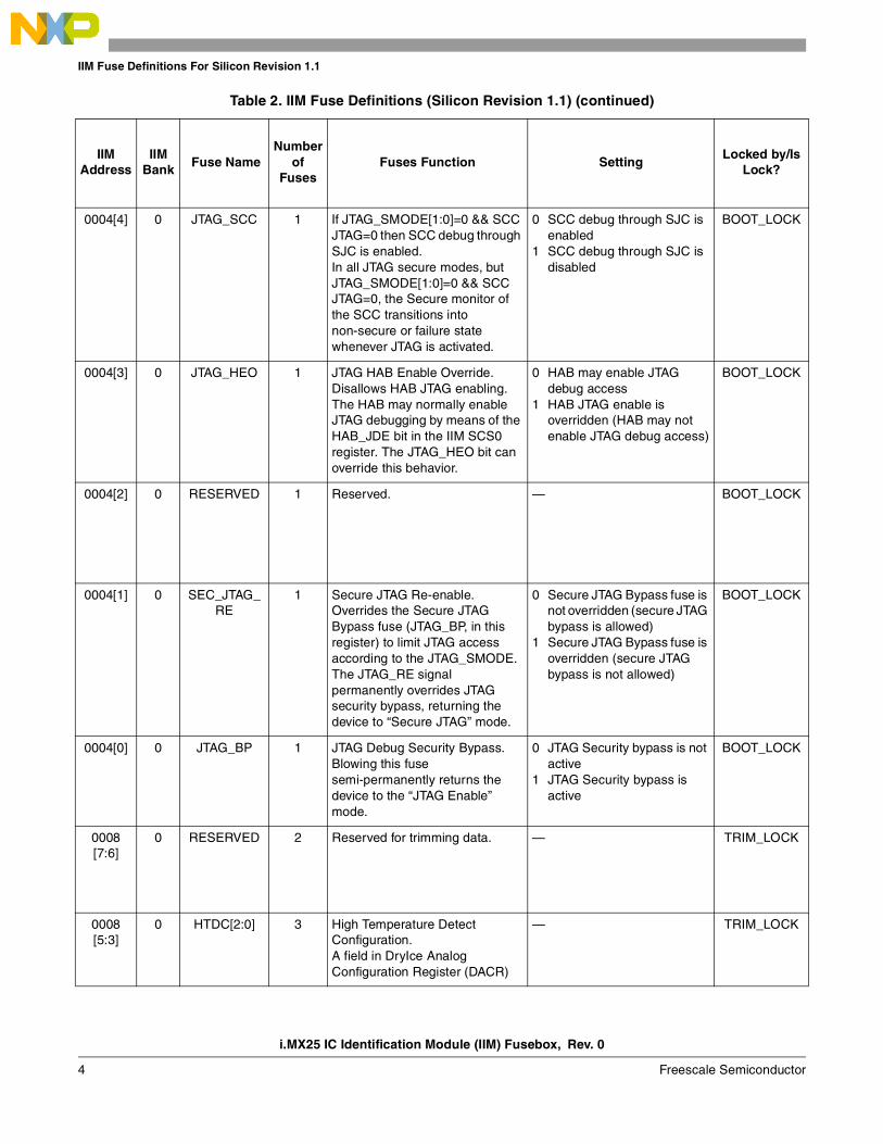
2 IIM Fuse Definitions For Silicon Revision 1.1Table 2 lists the fuse definitions for silicon revision 1.1.
Table 1. Fusebox Supply Current Parameters
Symbol Parameter Min Typ Max Units
FUSE_VDD1
1 The Fusebox read supply is connected to the supply of the full speed USBPY2_VDD. FUSE_VDD is only used for programming. Connect it to ground when not using it for programming.
Fusebox program supply voltage 3.0 3.6 3.6 V
Iprogram eFuse Program Current2:
Current to program one eFuse bit epm_avdd = 3.6 V
2 The current Iprogram is during program time (tprogram).
26 35 62 mA
Iread eFuse Read Current3
Current to read an 8-bit eFuse word vdd_fusebox = 3.3 V
3 The current Iread is present for approximately 50 ns of the read access to the 8-bit word.
— 12.5 15 mA
tprogram Program time for eFuse4
4 The program length is defined by the value defined in the epm_pgm_length[2:0] bits of the IIM module. The value to program is based on a 32 Hz clock source (4 × 1/32 kHz = 125 µs).
125 — — µs
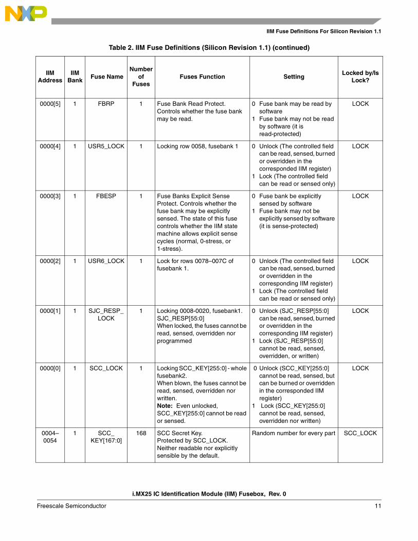
Table 2. IIM Fuse Definitions (Silicon Revision 1.1)
IIMAddress
IIMBank
Fuse NameNumber
of Fuses
Fuses Function SettingLocked by/Is
Lock?
0000[7] 0 FBWP 1 Fuse Bank Write Protect. Controls whether the fuse bank may be programmed.
0 Fuse bank may be programmed
1 Fuse bank may not be programmed (it is write-protected)
LOCK
0000[6] 0 FBOP 1 Fuse Bank Override Protect. Controls whether the fuse bank may be overridden.
0 Fuse bank may be overridden
1 Fuse bank may not be overridden (it is override-protected)
LOCK
0000[5] 0 FBRP 1 Fuse Bank Read Protect. Controls whether the fuse bank may be read.
0 Fuse bank may be read by software
1 Fuse bank may not be read by software (it is read-protected)
LOCK

i.MX25 IC Identification Module (IIM) Fusebox, Rev. 0
Freescale Semiconductor 3
IIM Fuse Definitions For Silicon Revision 1.1
0000[4] 0 TESTER_LOCK
1 Tester fuses.Burnt on the tester at the end of the wafer sort.Locking rows 001C-003C, fusebank 0.
0 Unlock (The controlled field can be read, sensed, burned or overridden in the corresponded IIM register)
1 Lock (The controlled field can be read or sensed only)
LOCK
0000[3] 0 FBESP 1 Fuse Banks Explicit Sense Protect. Controls whether the fuse bank may be explicitly sensed. The state of this fuse controls whether the IIM state machine allows explicit sense cycles (normal, 0-stress, or 1-stress).
0 Fuse bank be explicitly sensed by software
1 Fuse bank may not be explicitly sensed by software (it is sense-protected)
LOCK
0000[2] 0 MAC_ADDR_LOCK
1 Locking row 0068-007C, fusebank0
0 Unlock (The controlled field can be read, sensed, burned or overridden in the corresponded IIM register)
1 Lock (The controlled field can be read or sensed only)
LOCK
0000[1] 0 TRIM_LOCK 1 Locking rows 0008 0054-0064, fusebank0
0 Unlock (The controlled field can be read, sensed, burned or overridden in the corresponded IIM register)
1 Lock (The controlled field can be read or sensed only)
LOCK
0000[0] 0 BOOT_LOCK 1 Boot fuses, Locking rows 0004, 000C-0018, 0040-0044,fusebank0
0 Unlock (The controlled field can be read, sensed, burned or overridden in the corresponded IIM register)
1 Lock (The controlled field can be read or sensed only)
LOCK
0004[7] 0 SJC_DISABLE]
1 Disabling the Secure JTAG Controller module clock. This fuse is used to create highest JTAG security level, where JTAG is completely blocked.
0 Secure JTAG Controller enabled
1 Secure JTAG Controller disabled
BOOT_LOCK
0004[6:5]
0 JTAG_SMODE[1:0]
2 JTAG Security Mode. Controls the security mode of the JTAG debug interface.
00 JTAG enable mode01 Secure JTAG mode11 No debug mode
BOOT_LOCK
Table 2. IIM Fuse Definitions (Silicon Revision 1.1) (continued)
IIMAddress
IIMBank
Fuse NameNumber
of Fuses
Fuses Function SettingLocked by/Is
Lock?
i.MX25 IC Identification Module (IIM) Fusebox, Rev. 0
4 Freescale Semiconductor
IIM Fuse Definitions For Silicon Revision 1.1
0004[4] 0 JTAG_SCC 1 If JTAG_SMODE[1:0]=0 && SCC JTAG=0 then SCC debug through SJC is enabled.In all JTAG secure modes, but JTAG_SMODE[1:0]=0 && SCC JTAG=0, the Secure monitor of the SCC transitions into non-secure or failure state whenever JTAG is activated.
0 SCC debug through SJC is enabled
1 SCC debug through SJC is disabled
BOOT_LOCK
0004[3] 0 JTAG_HEO 1 JTAG HAB Enable Override. Disallows HAB JTAG enabling. The HAB may normally enable JTAG debugging by means of the HAB_JDE bit in the IIM SCS0 register. The JTAG_HEO bit can override this behavior.
0 HAB may enable JTAG debug access
1 HAB JTAG enable is overridden (HAB may not enable JTAG debug access)
BOOT_LOCK
0004[2] 0 RESERVED 1 Reserved. — BOOT_LOCK
0004[1] 0 SEC_JTAG_RE
1 Secure JTAG Re-enable. Overrides the Secure JTAG Bypass fuse (JTAG_BP, in this register) to limit JTAG access according to the JTAG_SMODE. The JTAG_RE signal permanently overrides JTAG security bypass, returning the device to “Secure JTAG” mode.
0 Secure JTAG Bypass fuse is not overridden (secure JTAG bypass is allowed)
1 Secure JTAG Bypass fuse is overridden (secure JTAG bypass is not allowed)
BOOT_LOCK
0004[0] 0 JTAG_BP 1 JTAG Debug Security Bypass. Blowing this fuse semi-permanently returns the device to the “JTAG Enable” mode.
0 JTAG Security bypass is not active
1 JTAG Security bypass is active
BOOT_LOCK
0008[7:6]
0 RESERVED 2 Reserved for trimming data. — TRIM_LOCK
0008[5:3]
0 HTDC[2:0] 3 High Temperature Detect Configuration. A field in DryIce Analog Configuration Register (DACR)
— TRIM_LOCK
Table 2. IIM Fuse Definitions (Silicon Revision 1.1) (continued)
IIMAddress
IIMBank
Fuse NameNumber
of Fuses
Fuses Function SettingLocked by/Is
Lock?
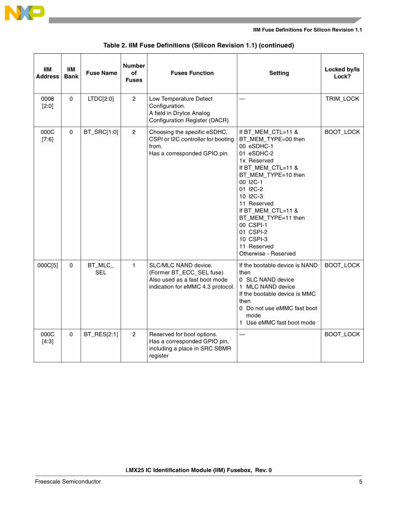
i.MX25 IC Identification Module (IIM) Fusebox, Rev. 0
Freescale Semiconductor 5
IIM Fuse Definitions For Silicon Revision 1.1
0008[2:0]
0 LTDC[2:0] 2 Low Temperature Detect Configuration. A field in DryIce Analog Configuration Register (DACR)
— TRIM_LOCK
000C[7:6]
0 BT_SRC[1:0] 2 Choosing the specific eSDHC, CSPI or I2C controller for booting from.Has a corresponded GPIO pin.
If BT_MEM_CTL=11 & BT_MEM_TYPE=00 then00 eSDHC-101 eSDHC-21x ReservedIf BT_MEM_CTL=11 & BT_MEM_TYPE=10 then00 I2C-101 I2C-210 I2C-311 ReservedIf BT_MEM_CTL=11 & BT_MEM_TYPE=11 then00 CSPI-101 CSPI-210 CSPI-311 ReservedOtherwise - Reserved
BOOT_LOCK
000C[5] 0 BT_MLC_SEL
1 SLC/MLC NAND device.(Former BT_ECC_SEL fuse)Also used as a fast boot mode indication for eMMC 4.3 protocol.
If the bootable device is NAND then0 SLC NAND device1 MLC NAND deviceIf the bootable device is MMC then0 Do not use eMMC fast boot
mode1 Use eMMC fast boot mode
BOOT_LOCK
000C[4:3]
0 BT_RES[2:1] 2 Reserved for boot options.Has a corresponded GPIO pin, including a place in SRC SBMR register
— BOOT_LOCK
Table 2. IIM Fuse Definitions (Silicon Revision 1.1) (continued)
IIMAddress
IIMBank
Fuse NameNumber
of Fuses
Fuses Function SettingLocked by/Is
Lock?
i.MX25 IC Identification Module (IIM) Fusebox, Rev. 0
6 Freescale Semiconductor
IIM Fuse Definitions For Silicon Revision 1.1
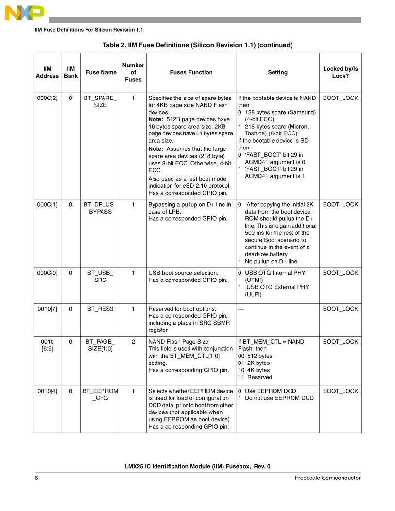
000C[2] 0 BT_SPARE_SIZE
1 Specifies the size of spare bytes for 4KB page size NAND Flash devices. Note: 512B page devices have 16 bytes spare area size, 2KB page devices have 64 bytes spare area size.
Note: Assumes that the large spare area devices (218 byte) uses 8-bit ECC. Otherwise, 4-bit ECC.
Also used as a fast boot mode indication for eSD 2.10 protocol.Has a corresponded GPIO pin.
If the bootable device is NAND then0 128 bytes spare (Samsung)
(4-bit ECC)1 218 bytes spare (Micron,
Toshiba) (8-bit ECC)If the bootable device is SD then0 ‘FAST_BOOT’ bit 29 in
ACMD41 argument is 01 ‘FAST_BOOT’ bit 29 in
ACMD41 argument is 1
BOOT_LOCK
000C[1] 0 BT_DPLUS_BYPASS
1 Bypassing a pullup on D+ line in case of LPB.Has a corresponded GPIO pin.
0 After copying the initial 2K data from the boot device, ROM should pullup the D+ line. This is to gain additional 500 ms for the rest of the secure Boot scenario to continue in the event of a dead/low battery.
1 No pullup on D+ line.
BOOT_LOCK
000C[0] 0 BT_USB_SRC
1 USB boot source selection.Has a corresponded GPIO pin.
0 USB OTG Internal PHY (UTMI)
1 USB OTG External PHY (ULPI)
BOOT_LOCK
0010[7] 0 BT_RES3 1 Reserved for boot options.Has a corresponded GPIO pin, including a place in SRC SBMR register
— BOOT_LOCK
0010[6:5]
0 BT_PAGE_SIZE[1:0]
2 NAND Flash Page Size. This field is used with conjunction with the BT_MEM_CTL[1:0] setting. Has a corresponding GPIO pin.
If BT_MEM_CTL = NAND Flash, then00 512 bytes01 2K bytes10 4K bytes11 Reserved
BOOT_LOCK
0010[4] 0 BT_EEPROM_CFG
1 Selects whether EEPROM device is used for load of configuration DCD data, prior to boot from other devices (not applicable when using EEPROM as boot device)Has a corresponding GPIO pin.
0 Use EEPROM DCD1 Do not use EEPROM DCD
BOOT_LOCK
Table 2. IIM Fuse Definitions (Silicon Revision 1.1) (continued)
IIMAddress
IIMBank
Fuse NameNumber
of Fuses
Fuses Function SettingLocked by/Is
Lock?

i.MX25 IC Identification Module (IIM) Fusebox, Rev. 0
Freescale Semiconductor 7
IIM Fuse Definitions For Silicon Revision 1.1
0010[3] 0 GPIO_BT_SEL
1 GPIO Boot Select. Determines whether certain boot fuse values are controlled from GPIO pins or IIM.
0 The fuse values are determined by GPIO pins
1 The fuse values are determined by fuses
BOOT_LOCK
0010[2:0]
0 HAB_TYPE[2:0]
3 Security Type. 001 Engineering (allows any code to be flashed and executed, even if does not have a valid signature)
100 Security Disabled (for internal/testing use)
Others Production (Security On)
BOOT_LOCK
0014[7] 0 BT_RES4 1 Reserved for boot options.Has a corresponded GPIO pin, including a place in SRC SBMR register
— BOOT_LOCK
0014[6:5]
0 BT_MEM_TYPE[1:0]
2 Boot Memory Type.Interpreted by boot ROM SW according to BT_MEM_CTL setting. Signals could also be interpreted by HW to alter delays and timing in support of direct boot.
If BT_MEM_CTL = WEIM, then00 NOR01 Reserved10 OneNand11 ReservedIf BT_MEM_CTL =NAND Flash00 3 address cycles01 4 address cycles10 5 address cycles11 ReservedIf BT_MEM_CTL = Expansion Card Device00 SD/MMC/MoviNAND HDD01 Reserved10 Serial ROM via I2C11 Serial ROM via SPI
BOOT_LOCK
0014[4:3]
0 BT_BUS_WIDTH
2 Bus width and muxed/unmuxed interface.Has a corresponded GPIO pin.
If BT_MEM_CTL=NAND then00 8 bit bus,01 16 bit bus1x ReservedIf BT_MEM_CTL=WEIM then00 16 bit addr/data muxed01 16 bit addr/data unmuxed i1x ReservedIf BT_MEM_CTL=SPI then00 2-addr word SPI (16-bit)01 3-addr word SPI (24-bit)1x Reserved
BOOT_LOCK
Table 2. IIM Fuse Definitions (Silicon Revision 1.1) (continued)
IIMAddress
IIMBank
Fuse NameNumber
of Fuses
Fuses Function SettingLocked by/Is
Lock?
i.MX25 IC Identification Module (IIM) Fusebox, Rev. 0
8 Freescale Semiconductor
IIM Fuse Definitions For Silicon Revision 1.1
0014[2:1]
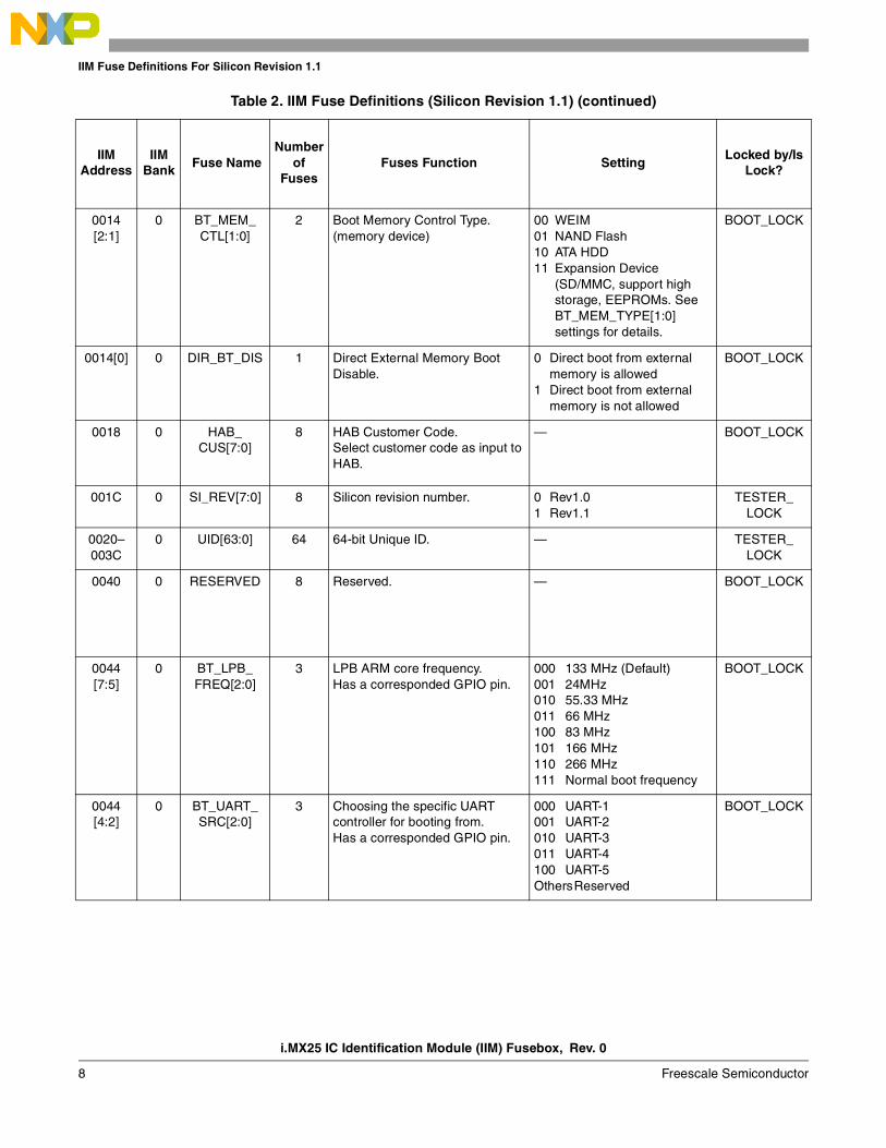
0 BT_MEM_CTL[1:0]
2 Boot Memory Control Type. (memory device)
00 WEIM01 NAND Flash10 ATA HDD11 Expansion Device
(SD/MMC, support high storage, EEPROMs. See BT_MEM_TYPE[1:0] settings for details.
BOOT_LOCK
0014[0] 0 DIR_BT_DIS 1 Direct External Memory Boot Disable.
0 Direct boot from external memory is allowed
1 Direct boot from external memory is not allowed
BOOT_LOCK
0018 0 HAB_CUS[7:0]
8 HAB Customer Code. Select customer code as input to HAB.
— BOOT_LOCK
001C 0 SI_REV[7:0] 8 Silicon revision number. 0 Rev1.01 Rev1.1
TESTER_LOCK
0020–003C
0 UID[63:0] 64 64-bit Unique ID. — TESTER_LOCK
0040 0 RESERVED 8 Reserved. — BOOT_LOCK
0044[7:5]
0 BT_LPB_FREQ[2:0]
3 LPB ARM core frequency.Has a corresponded GPIO pin.
000 133 MHz (Default)001 24MHz010 55.33 MHz011 66 MHz100 83 MHz101 166 MHz110 266 MHz111 Normal boot frequency
BOOT_LOCK
0044[4:2]
0 BT_UART_SRC[2:0]
3 Choosing the specific UART controller for booting from.Has a corresponded GPIO pin.
000 UART-1001 UART-2010 UART-3011 UART-4100 UART-5OthersReserved
BOOT_LOCK
Table 2. IIM Fuse Definitions (Silicon Revision 1.1) (continued)
IIMAddress
IIMBank
Fuse NameNumber
of Fuses
Fuses Function SettingLocked by/Is
Lock?
i.MX25 IC Identification Module (IIM) Fusebox, Rev. 0
Freescale Semiconductor 9
IIM Fuse Definitions For Silicon Revision 1.1
0044[1:0]
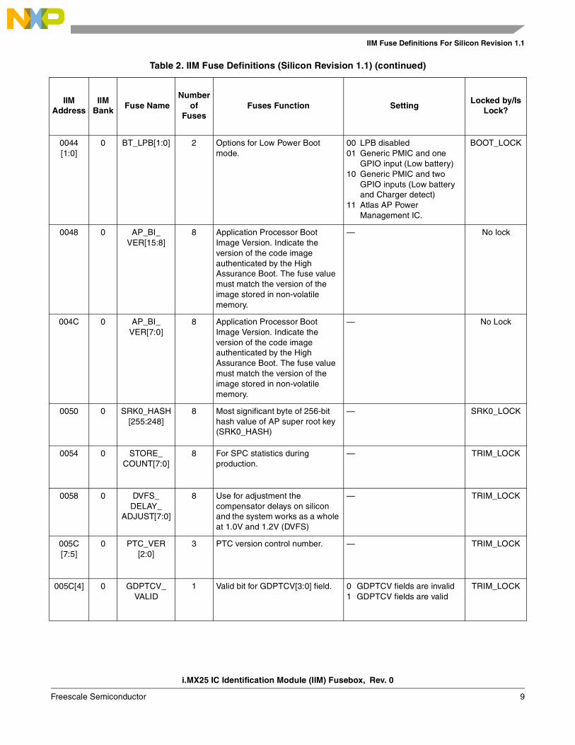
0 BT_LPB[1:0] 2 Options for Low Power Boot mode.
00 LPB disabled01 Generic PMIC and one
GPIO input (Low battery)10 Generic PMIC and two
GPIO inputs (Low battery and Charger detect)
11 Atlas AP Power Management IC.
BOOT_LOCK
0048 0 AP_BI_VER[15:8]
8 Application Processor Boot Image Version. Indicate the version of the code image authenticated by the High Assurance Boot. The fuse value must match the version of the image stored in non-volatile memory.
— No lock
004C 0 AP_BI_VER[7:0]
8 Application Processor Boot Image Version. Indicate the version of the code image authenticated by the High Assurance Boot. The fuse value must match the version of the image stored in non-volatile memory.
— No Lock
0050 0 SRK0_HASH[255:248]
8 Most significant byte of 256-bit hash value of AP super root key (SRK0_HASH)
— SRK0_LOCK
0054 0 STORE_COUNT[7:0]
8 For SPC statistics during production.
— TRIM_LOCK
0058 0 DVFS_DELAY_
ADJUST[7:0]
8 Use for adjustment the compensator delays on silicon and the system works as a whole at 1.0V and 1.2V (DVFS)
— TRIM_LOCK
005C[7:5]
0 PTC_VER[2:0]
3 PTC version control number. — TRIM_LOCK
005C[4] 0 GDPTCV_VALID
1 Valid bit for GDPTCV[3:0] field. 0 GDPTCV fields are invalid1 GDPTCV fields are valid
TRIM_LOCK
Table 2. IIM Fuse Definitions (Silicon Revision 1.1) (continued)
IIMAddress
IIMBank
Fuse NameNumber
of Fuses
Fuses Function SettingLocked by/Is
Lock?

i.MX25 IC Identification Module (IIM) Fusebox, Rev. 0
10 Freescale Semiconductor
IIM Fuse Definitions For Silicon Revision 1.1
005C[3:0]
0 GDPTCV[3:0] 4 GP domain DPTC/SPC Test Voltage. Indicates the testing voltage in production, using DPTC/SPC of GP transistor technology.
0000 1.0V0001 0.975V...1111 0.625V
TRIM_LOCK
0060[7:5]
0 VRC[2:0] 3 Voltage Reference Configuration.A field in DryIce Analog Configuration Register (DACR)
— TRIM_LOCK
0060[4] 0 LDPTCV_VALID
1 Valid bit for LDPTCV[3:0] field. 0 LDPTCV fields are invalid1 LDPTCV fields are valid
TRIM_LOCK
0060[3:0]
0 LDPTCV[3:0] 3 LP domain DPTC Test Voltage. Indicates the testing voltage in production, using DPTC of LP transistor technology.
0000 1.2V0001 1.175V...1111 0.825V
TRIM_LOCK
0064[7:5]
0 RESERVED 3 Reserved. — TRIM_LOCK
0064[4] 0 CPFA 1 Well Bias Charge Pump Frequency Adjust. Adjusting the frequency of the internal free-running oscillator.
0 Low frequency operation1 High frequency operation
TRIM_LOCK
0064[3:0]
0 CPSPA[3:0] 4 Well Bias Charge Pump Set Point Adjustment. Allows optimization of the AWB for the mass production. Allows a back bias set point scheme to be implemented.
— TRIM_LOCK
0068-007C
0 MAC_ADDR[47:0]
48 Ethernet MAC Address. — MAC_ADDR_LOCK
0000[7] 1 FBWP 1 Fuse Bank Write Protect. Controls whether the fuse bank may be programmed.
0 Fuse bank may be programmed
1 Fuse bank may not be programmed (it is write-protected)
LOCK
0000[6] 1 FBOP 1 Fuse Bank Override Protect. Controls whether the fuse bank may be overridden.
0 Fuse bank may be overridden
1 Fuse bank may not be overridden (it is override-protected)
LOCK
Table 2. IIM Fuse Definitions (Silicon Revision 1.1) (continued)
IIMAddress
IIMBank
Fuse NameNumber
of Fuses
Fuses Function SettingLocked by/Is
Lock?
i.MX25 IC Identification Module (IIM) Fusebox, Rev. 0
Freescale Semiconductor 11
IIM Fuse Definitions For Silicon Revision 1.1
0000[5] 1 FBRP 1 Fuse Bank Read Protect. Controls whether the fuse bank may be read.
0 Fuse bank may be read by software
1 Fuse bank may not be read by software (it is read-protected)
LOCK
0000[4] 1 USR5_LOCK 1 Locking row 0058, fusebank 1 0 Unlock (The controlled field can be read, sensed, burned or overridden in the corresponded IIM register)
1 Lock (The controlled field can be read or sensed only)
LOCK
0000[3] 1 FBESP 1 Fuse Banks Explicit Sense Protect. Controls whether the fuse bank may be explicitly sensed. The state of this fuse controls whether the IIM state machine allows explicit sense cycles (normal, 0-stress, or 1-stress).
0 Fuse bank be explicitly sensed by software
1 Fuse bank may not be explicitly sensed by software (it is sense-protected)
LOCK
0000[2] 1 USR6_LOCK 1 Lock for rows 0078–007C of fusebank 1.
0 Unlock (The controlled field can be read, sensed, burned or overridden in the corresponding IIM register)
1 Lock (The controlled field can be read or sensed only)
LOCK
0000[1] 1 SJC_RESP_LOCK
1 Locking 0008-0020, fusebank1.SJC_RESP[55:0]When locked, the fuses cannot be read, sensed, overridden nor programmed
0 Unlock (SJC_RESP[55:0] can be read, sensed, burned or overridden in the corresponding IIM register)
1 Lock (SJC_RESP[55:0] cannot be read, sensed, overridden, or written)
LOCK
0000[0] 1 SCC_LOCK 1 Locking SCC_KEY[255:0] - whole fusebank2.When blown, the fuses cannot be read, sensed, overridden nor written.Note: Even unlocked, SCC_KEY[255:0] cannot be read or sensed.
0 Unlock (SCC_KEY[255:0] cannot be read, sensed, but can be burned or overridden in the corresponded IIM register)
1 Lock (SCC_KEY[255:0] cannot be read, sensed, overridden nor written)
LOCK
0004–0054
1 SCC_KEY[167:0]
168 SCC Secret Key. Protected by SCC_LOCK. Neither readable nor explicitly sensible by the default.
Random number for every part SCC_LOCK
Table 2. IIM Fuse Definitions (Silicon Revision 1.1) (continued)
IIMAddress
IIMBank
Fuse NameNumber
of Fuses
Fuses Function SettingLocked by/Is
Lock?

i.MX25 IC Identification Module (IIM) Fusebox, Rev. 0
12 Freescale Semiconductor
IIM Fuse Definitions For Silicon Revision 1.1
0058 1 USR5[7:0] 8 Fuses available for software/customers.
— USR5_LOCK
005C-0074
1 SJC_RESP[55:0]
56 Response reference value for the secure JTAG controller.
— SJC_RESP_LOCK
(locks also for read, scan and
sense)
0078- 007C
1 USR6[15:0] 16 Fuses available for software/customers.
— USR6_LOCK
0000[7] 2 FBWP 1 Fuse Bank Write Protect. Controls whether the fuse bank may be programmed.
0 Fuse bank may be programmed
1 Fuse bank may not be programmed (it is write protected)
LOCK
0000[6] 2 FBOP 1 Fuse Bank Override Protect. Controls whether the fuse bank may be overridden.
0 Fuse bank may be overridden
1 Fuse bank may not be overridden (it is override protected)
LOCK
0000[5] 2 FBRP 1 Fuse Bank Read Protect. Controls whether the fuse bank may be read.
0 Fuse bank may be read by software
1 Fuse bank may not be read by software (it is read protected)
LOCK
0000[4] 2 RESERVED 1 Reserved — No Lock
0000[3] 2 FBESP 1 Fuse Banks Explicit Sense Protect. Controls whether the fuse bank may be explicitly sensed. The state of this fuse controls whether the IIM state machine allows explicit sense cycles (normal, 0-stress, or 1-stress).
0 Fuse bank be explicitly sensed by software
1 Fuse bank may not be explicitly sensed by software (it is sense protected)
LOCK
0000[2] 2 RESERVED 1 Reserved. — No lock
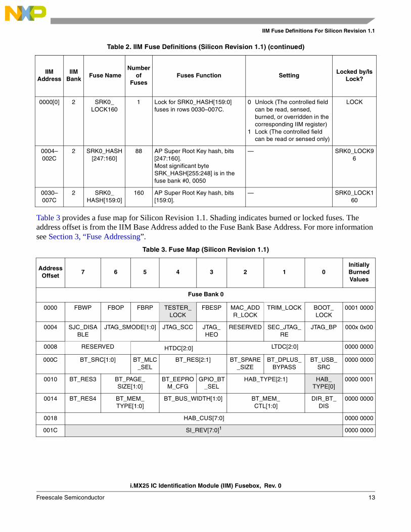
0000[1] 2 SRK0_LOCK96
1 Lock for SRK_HASH[255:160] fuses in row 0050, fusebank0 and in rows 0004-002C, fusebank3.
0 Fuse bank is sensible.1 Fuse bank is explicit
sense-protected.This lock does not protect against reading.
LOCK
Table 2. IIM Fuse Definitions (Silicon Revision 1.1) (continued)
IIMAddress
IIMBank
Fuse NameNumber
of Fuses
Fuses Function SettingLocked by/Is
Lock?
i.MX25 IC Identification Module (IIM) Fusebox, Rev. 0
Freescale Semiconductor 13
IIM Fuse Definitions For Silicon Revision 1.1
Table 3 provides a fuse map for Silicon Revision 1.1. Shading indicates burned or locked fuses. The address offset is from the IIM Base Address added to the Fuse Bank Base Address. For more information see Section 3, “Fuse Addressing”.
0000[0] 2 SRK0_LOCK160
1 Lock for SRK0_HASH[159:0] fuses in rows 0030–007C.
0 Unlock (The controlled field can be read, sensed, burned, or overridden in the corresponding IIM register)
1 Lock (The controlled field can be read or sensed only)
LOCK
0004–002C
2 SRK0_HASH[247:160]
88 AP Super Root Key hash, bits [247:160].Most significant byte SRK_HASH[255:248] is in the fuse bank #0, 0050
— SRK0_LOCK96
0030–007C
2 SRK0_HASH[159:0]
160 AP Super Root Key hash, bits [159:0].
— SRK0_LOCK160
Table 3. Fuse Map (Silicon Revision 1.1)
Address Offset
7 6 5 4 3 2 1 0Initially Burned Values
Fuse Bank 0
0000 FBWP FBOP FBRP TESTER_LOCK
FBESP MAC_ADDR_LOCK
TRIM_LOCK BOOT_LOCK
0001 0000
0004 SJC_DISABLE
JTAG_SMODE[1:0] JTAG_SCC JTAG_HEO
RESERVED SEC_JTAG_RE
JTAG_BP 000x 0x00
0008 RESERVED HTDC[2:0] LTDC[2:0] 0000 0000
000C BT_SRC[1:0] BT_MLC_SEL
BT_RES[2:1] BT_SPARE_SIZE
BT_DPLUS_BYPASS
BT_USB_SRC
0000 0000
0010 BT_RES3 BT_PAGE_SIZE[1:0]
BT_EEPROM_CFG
GPIO_BT_SEL
HAB_TYPE[2:1] HAB_TYPE[0]
0000 0001
0014 BT_RES4 BT_MEM_TYPE[1:0]
BT_BUS_WIDTH[1:0] BT_MEM_CTL[1:0]
DIR_BT_DIS
0000 0000
0018 HAB_CUS[7:0] 0000 0000
001C SI_REV[7:0]1 0000 0000
Table 2. IIM Fuse Definitions (Silicon Revision 1.1) (continued)
IIMAddress
IIMBank
Fuse NameNumber
of Fuses
Fuses Function SettingLocked by/Is
Lock?
i.MX25 IC Identification Module (IIM) Fusebox, Rev. 0
14 Freescale Semiconductor
IIM Fuse Definitions For Silicon Revision 1.1
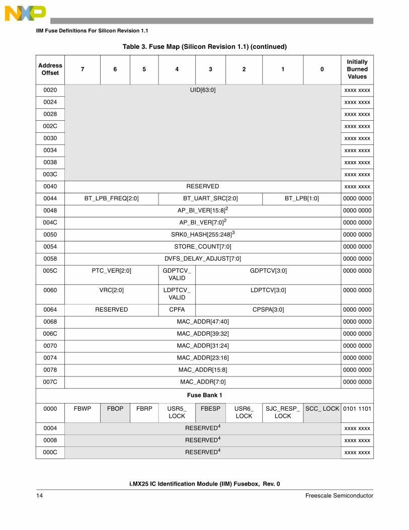
0020 UID[63:0] xxxx xxxx
0024 xxxx xxxx
0028 xxxx xxxx
002C xxxx xxxx
0030 xxxx xxxx
0034 xxxx xxxx
0038 xxxx xxxx
003C xxxx xxxx
0040 RESERVED xxxx xxxx
0044 BT_LPB_FREQ[2:0] BT_UART_SRC[2:0] BT_LPB[1:0] 0000 0000
0048 AP_BI_VER[15:8]2 0000 0000
004C AP_BI_VER[7:0]2 0000 0000
0050 SRK0_HASH[255:248]3 0000 0000
0054 STORE_COUNT[7:0] 0000 0000
0058 DVFS_DELAY_ADJUST[7:0] 0000 0000
005C PTC_VER[2:0] GDPTCV_VALID
GDPTCV[3:0] 0000 0000
0060 VRC[2:0] LDPTCV_VALID
LDPTCV[3:0] 0000 0000
0064 RESERVED CPFA CPSPA[3:0] 0000 0000
0068 MAC_ADDR[47:40] 0000 0000
006C MAC_ADDR[39:32] 0000 0000
0070 MAC_ADDR[31:24] 0000 0000
0074 MAC_ADDR[23:16] 0000 0000
0078 MAC_ADDR[15:8] 0000 0000
007C MAC_ADDR[7:0] 0000 0000
Fuse Bank 1
0000 FBWP FBOP FBRP USR5_LOCK
FBESP USR6_LOCK
SJC_RESP_LOCK
SCC_ LOCK 0101 1101
0004 RESERVED4 xxxx xxxx
0008 RESERVED4 xxxx xxxx
000C RESERVED4 xxxx xxxx
Table 3. Fuse Map (Silicon Revision 1.1) (continued)
Address Offset
7 6 5 4 3 2 1 0Initially Burned Values
i.MX25 IC Identification Module (IIM) Fusebox, Rev. 0
Freescale Semiconductor 15
IIM Fuse Definitions For Silicon Revision 1.1
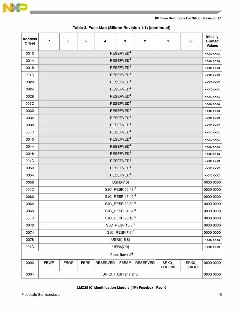
0010 RESERVED4 xxxx xxxx
0014 RESERVED4 xxxx xxxx
0018 RESERVED4 xxxx xxxx
001C RESERVED4 xxxx xxxx
0020 RESERVED4 xxxx xxxx
0024 RESERVED4 xxxx xxxx
0028 RESERVED4 xxxx xxxx
002C RESERVED4 xxxx xxxx
0030 RESERVED4 xxxx xxxx
0034 RESERVED4 xxxx xxxx
0038 RESERVED4 xxxx xxxx
003C RESERVED4 xxxx xxxx
0040 RESERVED4 xxxx xxxx
0044 RESERVED4 xxxx xxxx
0048 RESERVED4 xxxx xxxx
004C RESERVED4 xxxx xxxx
0050 RESERVED4 xxxx xxxx
0054 RESERVED4 xxxx xxxx
0058 USR5[7:0] 0000 0000
005C SJC_RESP[55:48]5 0000 0000
0060 SJC_RESP[47:40]5 0000 0000
0064 SJC_RESP[39:32]5 0000 0000
0068 SJC_RESP[31:24]5 0000 0000
006C SJC_RESP[23:16]5 0000 0000
0070 SJC_RESP[15:8]5 0000 0000
0074 SJC_RESP[7:0]5 0000 0000
0078 USR6[15:8] xxxx xxxx
007C USR6[7:0] xxxx xxxx
Fuse Bank 26
0000 FBWP FBOP FBRP RESERVED FBESP RESERVED SRK0_ LOCK96
SRK0_ LOCK160
0000 0000
0004 SRK0_HASH[247:240] 0000 0000
Table 3. Fuse Map (Silicon Revision 1.1) (continued)
Address Offset
7 6 5 4 3 2 1 0Initially Burned Values

i.MX25 IC Identification Module (IIM) Fusebox, Rev. 0
16 Freescale Semiconductor
IIM Fuse Definitions For Silicon Revision 1.1
0008 SRK0_HASH[239:232] 0000 0000
000C SRK0_HASH[231:224] 0000 0000
0010 SRK0_HASH[223:216] 0000 0000
0014 SRK0_HASH[215:208] 0000 0000
0018 SRK0_HASH[207:200] 0000 0000
001C SRK0_HASH[199:192] 0000 0000
0020 SRK0_HASH[191:184] 0000 0000
0024 SRK0_HASH[183:176] 0000 0000
0028 SRK0_HASH[175:168] 0000 0000
002C SRK0_HASH[167:160] 0000 0000
0030 SRK0_HASH[159:152] 0000 0000
0034 SRK0_HASH[151:144] 0000 0000
0038 SRK0_HASH[143:136] 0000 0000
003C SRK0_HASH[135:128] 0000 0000
0040 SRK0_HASH[127:120] 0000 0000
0044 SRK0_HASH[119:112] 0000 0000
0048 SRK0_HASH[111:104] 0000 0000
004C SRK0_HASH[103:96] 0000 0000
0050 SRK0_HASH[95:88] 0000 0000
0054 SRK0_HASH[87:80] 0000 0000
0058 SRK0_HASH[79:72] 0000 0000
005C SRK0_HASH[71:64] 0000 0000
0060 SRK0_HASH[63:56] 0000 0000
0064 SRK0_HASH[55:48] 0000 0000
0068 SRK0_HASH[47:40] 0000 0000
006C SRK0_HASH[39:32] 0000 0000
0070 SRK0_HASH[31:24] 0000 0000
0074 SRK0_HASH[23:16] 0000 0000
0078 SRK0_HASH[15:8] 0000 0000
007C SRK0_HASH[7:0] 0000 0000
1 According to the chip silicon revision, 1 = Rev 1.12 Boot Image Version
Table 3. Fuse Map (Silicon Revision 1.1) (continued)
Address Offset
7 6 5 4 3 2 1 0Initially Burned Values
i.MX25 IC Identification Module (IIM) Fusebox, Rev. 0
Freescale Semiconductor 17
Fuse Addressing
3 Fuse AddressingThe IIM module base address register is 0x53FF_0000. All registers are 8-bit wide, but addressable on 32-bit boundaries.
The IIM contains three fuse banks. Each bank contains 256 8-bit rows for a total of 2048 fuses per bank. Each fuse row is addressable on a 32-bit boundary, meaning that Fuse Row Index 0 is at Fuse Row Offset 0x0, Fuse Row Index 1 is at Fuse Row Offset 0x4, Fuse Row Index 2 is at Fuse Row Offset 0x8, and so on.
Fuse Bank 0 is located at offset 0x0800 from the IIM base address (0x53FF_0000). Fuse Bank 1 is located at offset 0x0C00. Fuse Bank 2 is located at offset 0x1000.
For example, the absolute address of Fuse Row 0xC at Bank 0 is 0x53FF_0000 + 0x0800 + 0xC == 0x53FF_080C. Keep in mind that the Fuse Row Index is 3.
4 Fuse Programming ProcedureFuse programming is accomplished using the following procedure:
1. Define the fuse bit address by writing to the upper address (UA) and lower address (LA) registers.
— UA register is located at 0x53FF_0014. LA register is located at 0x53FF_0018.
— UA[5:3] selects the fuse bank.
— UA[2:0] provides the most significant portion of the Fuse Row Index within the bank.
— LA[7:3] provides the least significant portion of the Fuse Row Index within the bank.
— LA[2:0] selects the bit position within the selected row (or fuse byte).
2. Write 0xAA to the program protection register (PRG_P), which is located at address 0x53FF_0028.
This register is used to protect against accidental fuse programming. The fuses can be blown only when the value of this register is 0xAA. Software should only program this register to 0xAA while actively blowing fuses. After the program operation is complete, immediately reprogram this register to a different value.
3. Enable and start fuse programming using the fuse control register (FCTL), which is located at address 0x53FF_0010. Writing 0x71 to this register commands the IIM to blow the fuse.
4. Wait until fuse programming is finished by IIM. When bit 1 of the status register (STAT) equals one, the program operation has finished. STAT is located at address 0x53FF_0000.
5. Clear bit 1 of STAT by writing “1” to it.
6. Write any value other than 0xAA to PRG_P register to prevent inadvertent fuse programming.
7. Check if there were errors by reading the content of the module errors register (ERR), which is located at address 0x53FF_0008. If bits[7:1] are all zeros, no error occurred.
3 Most significant byte of 256-bit SRKO_HASH4 Unreadable SCC Key5 Response reference value for the secure JTAG controller. Cannot be read, overridden, or programmed after SJC_REP_LOCK
is blown.6 Bits 247.0 of Hash of super-root key stored in FLASH
i.MX25 IC Identification Module (IIM) Fusebox, Rev. 0
18 Freescale Semiconductor
Fuse Sensing Procedure
5 Fuse Sensing ProcedureWhile fuse programming blows fuses one bit at a time, fuse sensing or reading always works at a byte boundary. There are two methods for reading fuse values: direct register address dereferencing and explicit fuse sensing.
5.1 Reading Fuses Using Direct Address DereferencingDirect register address dereferencing is accomplished by calculating the absolute fuse address and reading the content of the register using standard pointer dereferencing methods. For example, the fuse row located at offset 0x10 from fuse bank 0 can be read with the following C code:
char fuse_byte = *(char *) (0x53FF0000 + 0x0800 + 0x10);
5.2 Reading Fuses Using Explicit SensingExplicit sensing is accomplished using the following procedure:
1. Write something other than 0xAA to PRG_P register to prevent fuses from being blown inadvertently.
2. Define the fuse row (or byte) address by writing to the upper address and lower address registers.
— UA[5:3] selects the fuse bank.
— UA[2:0] provides the most significant portion of the Fuse Row Index within the bank.
— LA[7:3] provides the least significant portion of the Fuse Row Index within the bank.
— LA [2:0] is disregarded during fuse sensing operations because it always reads all 8 bits within the given fuse row.
3. Set the SENS strength to the fuse control register (FCTL), which triggers a sense cycle. Only one of bits[3:1] can be set to 1 to start a read cycle.
4. Wait until SNSD bit from the status register (STAT[0]) equals one.
5. Write “1” to SNSD bit from the status register (STAT[0]) to clear it.
6. Check for errors by reading the content of the module errors register (ERR), which is located at address 0x53FF_0008. If bits[7:1] are all zeros, no error occurred.
7. The fuse row (or byte) value can be retrieved by reading the SDAT register, which is located at address 0x53FF_001C.
6 Sample CodeThe following source code describes how to do fuse programming and fuse sensing in C programming language.
#define setmem8(address, value) *(volatile unsigned char *)address = (unsigned char)value#define readmem8(address) (*(volatile unsigned char *)address)
//Important IIM register definitions.#define IIM_BASE_ADDRESS (0x53FF0000)
i.MX25 IC Identification Module (IIM) Fusebox, Rev. 0
Freescale Semiconductor 19
Sample Code
#define IIM_UPPER_ADDRESS_REG (IIM_BASE_ADDRESS + 0x14)#define IIM_LOWER_ADDRESS_REG (IIM_BASE_ADDRESS + 0x18)#define IIM_PRG_P_REG (IIM_BASE_ADDRESS + 0x28)#define IIM_FCTL_REG (IIM_BASE_ADDRESS + 0x10)#define IIM_STAT_REG (IIM_BASE_ADDRESS + 0x00)#define IIM_ERR_REG (IIM_BASE_ADDRESS + 0x08)#define IIM_SDAT_REG (IIM_BASE_ADDRESS + 0x1C)
typedef enum{
ESNS_1 = 2,ESNS_0 = 4,ESNS_N = 8 //Normal Sensing
}e_sens_strength;
typedef enum{
FUSE_BANK_0,FUSE_BANK_1,FUSE_BANK_2,MAX_FUSE_BANK //MX25 only has 3 fuse banks, 0, 1 and 2.
}e_fuse_banks;
//fuse_bank is the fuse bank index. MX25 only has 3 banks. That's why they've been enumerated.//fuse_row_addr: represents the address of the row where we are going to blow a fuse.// Each Row addresses one byte worth of data. This means one row contains 8 fuses ready to be blown!// Row Index 0 is Row Address 0x0// Row Index 1 is Row Address 0x4// Row Index 2 is Row Address 0x8// Row Index 3 is Row Address 0xC// ... And so on
//fuse_bit_addr: A number from 0 to 7 that represent the fuse bit index that we are going to blow or sense.static void set_fuse_address(e_fuse_banks fuse_bank, unsigned short fuse_row_addr, unsigned char fuse_bit_addr){
unsigned char upper_addr;unsigned char lower_addr;unsigned char fuse_index;
//A fuse bank contains 256 fuse rows. for a total of 2048 fuse bits.//Dividing the fuse_address by 4 will give us the fuse index.fuse_index = (unsigned char)(fuse_row_addr >> 2);
upper_addr = ( (unsigned char)fuse_bank << 3);upper_addr |= ((fuse_index >> 5) & 0x7);
lower_addr = ((fuse_index & 0x1F) << 3);lower_addr |= (fuse_bit_addr & 0x7);
//write address to UA LA registersetmem8(IIM_UPPER_ADDRESS_REG, upper_addr);setmem8(IIM_LOWER_ADDRESS_REG, lower_addr);
}
//Returns 0 when Successful.
i.MX25 IC Identification Module (IIM) Fusebox, Rev. 0
20 Freescale Semiconductor
Sample Code
unsigned char fuse_bit_program(e_fuse_banks fuse_bank,unsigned char fuse_row_addr, unsigned char fuse_bit_addr)
{unsigned char error;
//Define the fuse bit address that we want to program.set_fuse_address(fuse_bank, fuse_row_addr, fuse_bit_addr);
//write 0xAA to Program Protection Register (PRG_P) register//The value 0xAA is an arbitrarily chosen value that needs to be written//to the register so the fuse program operation actually works.//This helps prevent to blow fuse by mistake.
setmem8(IIM_PRG_P_REG, 0xAA);//Enable and Start Fuse Programming via Fuse Control Register(FCTL)setmem8(IIM_FCTL_REG,0x71);
//Wait until fuse blowing is finished.while( (readmem8(IIM_STAT_REG) & 0x2) == 0 );
//Write 1 to clear PRGD bitsetmem8(IIM_STAT_REG,0x02);
//Very good to do too. for safety.setmem8(IIM_PRG_P_REG, 0x0);
//Check Error status.error = readmem8(IIM_ERR_REG);if (error & 0xFE)
{
//Clear Error Status Register. By writing the same value we got.//These are Clear-on-Write type of bits.
setmem8(IIM_ERR_REG, error);//Some error occurred.return error;
}
//No error at all.return 0;
}
//Returns the value of all the fuses (8 fuses or 8 bits)// contained in fuse_row_addr.unsigned char fuse_byte_read(e_fuse_banks fuse_bank,
unsigned char fuse_row_addr, e_sens_strength sens_strength)
{unsigned char error;unsigned char fuse_byte_value;
//Just in case.// Write something different than 0xAA to IIM_PRG_P_REG to prevent//fuses from being blown inadvertently.setmem8(IIM_PRG_P_REG, 0x0);
i.MX25 IC Identification Module (IIM) Fusebox, Rev. 0
Freescale Semiconductor 21
Revision History
//Define the fuse row address that we want to read.set_fuse_address(fuse_bank, fuse_row_addr, 0);
//Set the SENS strength to the Fuse Control Register// which will also trigger a sense cycle.
setmem8(IIM_FCTL_REG, sens_strength);
// wait for SNSD bit to set. While this is 0,// it means the sensing has not finished. while ( (readmem8(IIM_STAT_REG) & 0x1) == 0 );
//Write 1 to SNSD bit in the STAT register. This is the way to clear it.setmem8(IIM_STAT_REG,0x01);
//Was there an error??error = readmem8(IIM_ERR_REG);if (error & 0xFE)
{//Clear Error Status Register. By writing the same value we got.//These are clear on Write type of bits.
setmem8(IIM_ERR_REG, error);
while (1); //READ ERROR. LOOP ForEver.}
//Read the byte we wanted.fuse_byte_value = readmem8(IIM_SDAT_REG);
return fuse_byte_value;
}
The following source code shows how to blow the HAB_TYPE[0] fuse, available for Silicon Revision 1.1, using the fuse_bit_program function defined above:
//Blow the HAB_TYPE Fuse. Bit 0 , of Fuse Row 0x 10 in FuseBank 0unsigned char error = fuse_bit_program(FUSE_BANK_0, 0x10 , 0 );
The following source code shows how to explicitly sense the HAB_TYPE[0] fuse using the fuse_byte_read function defined above:
unsigned char fuse_byte_value = fuse_byte_read(FUSE_BANK_0, 0x10 , ESNS_N);//If the HAB_TYPE[0] fuse is blown, fuse_byte_value bit 0 must be on.//In case where no other fuses are blown in this byte then it will be 0x1 .
As mentioned before, the same fuse row can also be read using direct register address dereferencing, which is shown in the following code:
unsigned char fuse_byte_value = *(unsigned char *)(0x53FF0000 + 0x0800 + 0x10 );
7 Revision HistoryTable 4. Document Revision History
Rev.Number
Date Substantive Change(s)
0 06/2009 Initial Release, based on version for i.MX35

i.MX25 IC Identification Module (IIM) Fusebox, Rev. 0
22 Freescale Semiconductor
Revision History
THIS PAGE INTENTIONALLY LEFT BLANK

i.MX25 IC Identification Module (IIM) Fusebox, Rev. 0
Freescale Semiconductor 23
Revision History
THIS PAGE INTENTIONALLY LEFT BLANK
Document Number: AN3682Rev. 006/2009
Information in this document is provided solely to enable system and software
implementers to use Freescale Semiconductor products. There are no express or
implied copyright licenses granted hereunder to design or fabricate any integrated
circuits or integrated circuits based on the information in this document.
Freescale Semiconductor reserves the right to make changes without further notice to
any products herein. Freescale Semiconductor makes no warranty, representation or
guarantee regarding the suitability of its products for any particular purpose, nor does
Freescale Semiconductor assume any liability arising out of the application or use of
any product or circuit, and specifically disclaims any and all liability, including without
limitation consequential or incidental damages. “Typical” parameters which may be
provided in Freescale Semiconductor data sheets and/or specifications can and do
vary in different applications and actual performance may vary over time. All operating
parameters, including “Typicals” must be validated for each customer application by
customer’s technical experts. Freescale Semiconductor does not convey any license
under its patent rights nor the rights of others. Freescale Semiconductor products are
not designed, intended, or authorized for use as components in systems intended for
surgical implant into the body, or other applications intended to support or sustain life,
or for any other application in which the failure of the Freescale Semiconductor product
could create a situation where personal injury or death may occur. Should Buyer
purchase or use Freescale Semiconductor products for any such unintended or
unauthorized application, Buyer shall indemnify and hold Freescale Semiconductor
and its officers, employees, subsidiaries, affiliates, and distributors harmless against all
claims, costs, damages, and expenses, and reasonable attorney fees arising out of,
directly or indirectly, any claim of personal injury or death associated with such
unintended or unauthorized use, even if such claim alleges that Freescale
Semiconductor was negligent regarding the design or manufacture of the part.
How to Reach Us:
Home Page: www.freescale.com
Web Support: http://www.freescale.com/support
USA/Europe or Locations Not Listed: Freescale Semiconductor, Inc.Technical Information Center, EL5162100 East Elliot Road Tempe, Arizona 85284 1-800-521-6274 or+1-480-768-2130www.freescale.com/support
Europe, Middle East, and Africa:Freescale Halbleiter Deutschland GmbHTechnical Information CenterSchatzbogen 781829 Muenchen, Germany+44 1296 380 456 (English) +46 8 52200080 (English)+49 89 92103 559 (German)+33 1 69 35 48 48 (French) www.freescale.com/support
Japan: Freescale Semiconductor Japan Ltd. HeadquartersARCO Tower 15F1-8-1, Shimo-Meguro, Meguro-ku Tokyo 153-0064Japan 0120 191014 or+81 3 5437 [email protected]
Asia/Pacific: Freescale Semiconductor China Ltd. Exchange Building 23FNo. 118 Jianguo RoadChaoyang DistrictBeijing 100022China+86 10 5879 [email protected]
For Literature Requests Only:Freescale Semiconductor
Literature Distribution Center P.O. Box 5405Denver, Colorado 80217 1-800 441-2447 or+1-303-675-2140Fax: +1-303-675-2150LDCForFreescaleSemiconductor
@hibbertgroup.com
Freescale and the Freescale logo are trademarks or registered trademarks of Freescale Semiconductor, Inc. in the U.S. and other countries. ARM is the registered trademark of ARM Limited. All other product or service names are the property of their respective owners.
© Freescale Semiconductor, Inc., 2009. All rights reserved.