Embed Size (px)
Citation preview

10 ani de nanostiinta si nanotehnologie, Bucuresti 2010
National Institute for R&D in Microtechnologies126A, Erou Iancu Nicolae, 077190, Bucharest, RomaniaTel: +40 21 269 07 78Fax: +40 21 269 07 72www.imt.ro - www.imt.ro/MINAFAB
IMT-MINAFAB as a platform of interaction in nanoscience and nanotechnologies
Radu Popa, Dan Dascalu
Summary
• About IMT-MINAFAB in brief.
• Main facts, main figures.
• Major fields of research.
• Current projects.
• Equipment overview.
• Collaboration and perspectives.

About IMT-MINAFAB, in brief
• State of the art research infrastructure, operating since September 2008.
• Center of services for micro- and nanofabrication and • Platform of interaction as open-centre for research and education-by-
research, focused on multidisciplinary innovation and knowledge transfer to industry.
• Enables highly efficient exploitation of IMT's existing tangible and intangible assets in nano-science/technologies (clean-room facility, advanced equipments, knowledge and experience, partners and clients).
• Complex technological platform: CAD tools, mask shop sector, analysis and characterization, nanobio fabrication, reliability tests.
• Access is facilitated in a variety of ways, with notable accent on developing common R&D projects and on offering direct access of innovative companies to nanoscience and nanotechnology expertise and tools.
70nm

Main facts, main figures [1]
• Class 1000 clean room (220 sqm) for the mask shop and the most demanding technological processes.
• Class 100,000 clean room - so called “grey area” - (200 sqm), mostly for the characterization equipments.
• Class 10,000 clean room (120 sqm) for thin films by CVD techniques, RTP, etc. (to become operational).
• Accumulated total investment in equipments and infrastructure: about 9 M euro (2006-2009: 7 M euro; 2008: 3.5 M, mainly from Capacities projects).
• Large range of services. Main categories: micro/nanofabrication for devices and systemsinspection, analysis and characterization of surfaces, films, crystals, nanostructuresdesign, modeling and simulationcomplex RDI services - from design, to reliability testing

Main facts, main figures [2]
• Over 60 national users as partners in consortia, or based on bilateral agreements: 30 companies, 15 research institutes, 15 universities.
• Over 30 industrial users, as partners in consortia or contracted service users: Austria(1), Finland(1), France(1), Germany(8), Greece(1), Hungary(2), Italy(3), Poland(1), Slovakia(2), Spain(1), Sweden(6), The Netherlands(3), etc.
• Over 30 partners in research - FP6-7, bilateral projects: Belgium(2), Finland(1), France(2), Germany(11), Greece(1), Hungary(1), Italy(2), Ireland(1), Israel(1), Poland(1), Spain(1), The Netherlands(3), UK(1), Singapore(1), etc.
• Master courses and hands-on training for students of Polytechnic University of Bucharest.
• Operation of IMT-MINAFAB conforms with best technical/technological/ management standards (e.g., degree of decontamination, safety of operation and processes, equipment conditions and operation, access monitoring).
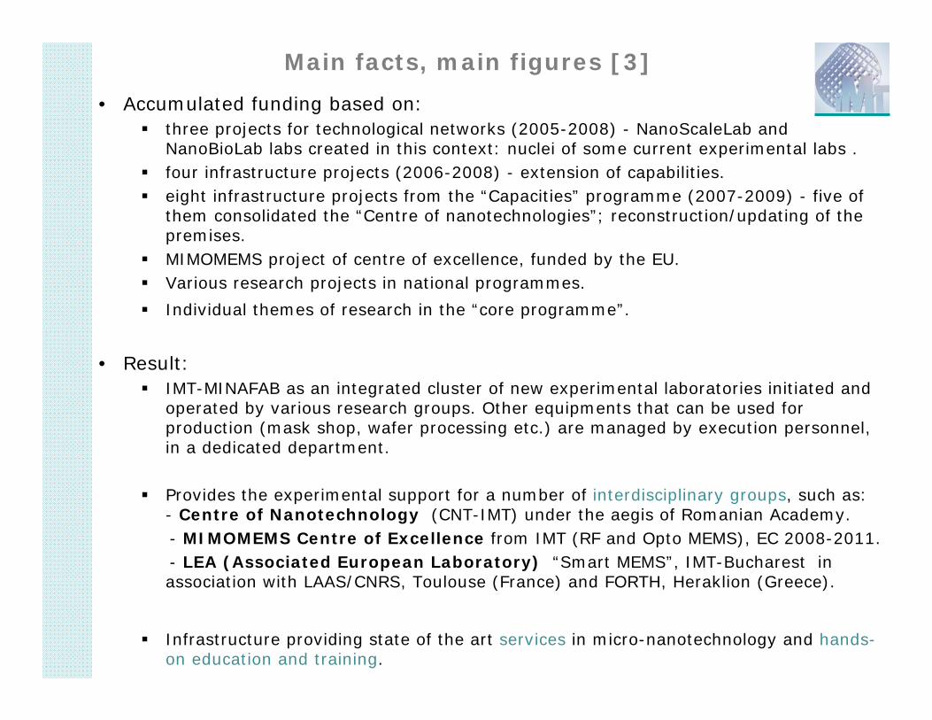
Main facts, main figures [3]
• Accumulated funding based on:three projects for technological networks (2005-2008) - NanoScaleLab and NanoBioLab labs created in this context: nuclei of some current experimental labs .four infrastructure projects (2006-2008) - extension of capabilities. eight infrastructure projects from the “Capacities” programme (2007-2009) - five of them consolidated the “Centre of nanotechnologies”; reconstruction/updating of the premises. MIMOMEMS project of centre of excellence, funded by the EU.Various research projects in national programmes.
Individual themes of research in the “core programme”.
• Result: IMT-MINAFAB as an integrated cluster of new experimental laboratories initiated and operated by various research groups. Other equipments that can be used for production (mask shop, wafer processing etc.) are managed by execution personnel, in a dedicated department.
Provides the experimental support for a number of interdisciplinary groups, such as: - Centre of Nanotechnology (CNT-IMT) under the aegis of Romanian Academy.- MIMOMEMS Centre of Excellence from IMT (RF and Opto MEMS), EC 2008-2011.- LEA (Associated European Laboratory) “Smart MEMS”, IMT-Bucharest in association with LAAS/CNRS, Toulouse (France) and FORTH, Heraklion (Greece).
Infrastructure providing state of the art services in micro-nanotechnology and hands-on education and training.

Major fields of R&D
• Collaborative multidisciplinary research, focusing on convergent micro-nano-bio technologies, based on structuring and characterization at the nanoscale.
• Components for nanoelectronics, photonics and microwavesnew fabrication technologies in Si, as well as in wide bandgap semiconductors, dielectrics, polymers. CNT/graphene-based nanostructures for nanoelectronics (transistors and chip interconnections). new concepts and structures for optical MEMS and RF-MEMS.
• Advanced nanomaterials and nanostructures for therapies, biosensing, energy and other industries
functionalized nanoporous materials, nanocomposite particles, microarrays.nanocomposite and film assemblies for fuel cells and photovoltaics.SAM's, immobilization and combined studies of molecular interactions.microfluidic components and biochips for biosensing and monitoring. functional films and nanocomposites for: neurosensing, constructions.

Major fields of R&D
• New technologies for fabrication and characterizationnanolithography, mask-free nano-connections, high aspect-ratio nanostructures.silicon nanoelectrodes, functional porous silicon, bio-active materials, field emission nanostructures.soft-lithography and replication. rapid prototyping: dip-pen nanolithography, laser micromachining, 3D and inkjet printing. nanomechanical characterization of materials.
IMT-MINAFAB currently provides a complex technological platform for basic research, application-oriented R&D and even small-scale production.

Current projects [1]
• FP6 projects
IMT was acting as coordinator, partner, associate partner or subcontractor.

Current projects [2]
• FP7 (and related) projects

Current projects [3]
►European Centre of Excellence in Microwave, Millimetre Wave and Optical Devices, based on Micro-Electro-Mechanical Systems for Advanced Communication Systems and Sensors –MIMOMEMS, Contract no. 202897, REGPOT, 2008-2011. Coordinator: IMT-Bucharest. Contact: Dr. Alexandru Muller ([email protected]).
►Enabling MEMS-MMIC technology for cost-effective multifunctional RF-system integration -MEMS-4-MMIC, Contract no.: 204101, STREP, ICT, 2008-2011. Coordinator: IMST GmbH, Germany. Coordinator: Dr. Stephen Trueman, CONSORZIO SAPIENZA INNOVAZIONE, Italy.IMT role: Partner. IMT Contact: Dr. Dan Neculoiu ([email protected]).
► Carbon nAnotube Technology for High-speed nExt-geneRation nano-InterconNEcts -CATHERINE, Contract no. 216215, STREP, ICT, 2008-2011. IMT role: Partner. IMT Contact: Adrian Dinescu ([email protected]).
► Flexible Patterning of Complex Micro Structures using Adaptive Embossing Technology –FlexPAET, IP, NMP, 2008-2010. Coordinator: Dr.-Ing. Christian Wenzel, Fraunhofer Gesellschaft zur Förderung der angewandten Forschung e.V. Fraunhofer Institut für Produktionstechnolgie (IPT), Germany. IMT role: Partner. IMT Contact: Dr. Dana Cristea ([email protected]).
►European scale infrastructure in NanoBiotechnology - EuroNanoBio, CSA, NMP, 2009-2010. Coordinator: Prof. Patrick Boisseau CEA, France. IMT role: Partner. IMT contact: Prof. Dan Dascalu ([email protected] ).

Current projects [4]
► Nanoelectronics for Safe, Fuel Efficient and Environment Friendly Automotive Solution –SE2A; ENIAC nanoelectronics - Coord: NXP Semiconductor Netherlands BV, The Netherlands. IMT contact: Dr. Alexandru Muller ([email protected]).
► Novel Gain Materials and Devices Based on III-V-N Compounds; COST Action - Coord: University of Essex, UK. IMT contact: Dr. Alexandru Muller ([email protected]),
► Micro Nano Technology Use by SME's- MINATUSE; EUREKA - Coord: IMEC, Belgium. IMT Contact: Ionica Miresteanu ([email protected]).
► Development of competences of educational staff by integrating operational tasks into measures of vocational training and further education – ComEd; Leonardo da Vinci -Coord: BWAW Thüringen GmbH, Germany. IMT Contact: Dr. Raluca Muller ([email protected]).
► A system-in-a-microfluidic package approach for focused diagnostic DNA microchips –DNASIP; ERA-NET - Coord: Université catolique de Louvain, Belgium. IMT contact: Monica Simion ([email protected]).
► Nanostructural carbonaceous films for cold emitters – NANOCAFE; ERA-NET - Coord: Industrial Institute of Electronics, Poland. IMT contact: Florea Craciunoiu ([email protected]).
Bilateral research cooperation with organizations from: Italy, France, Belgium, UK, Japan, Singapore, South-Africa.

Equipment overview [1]
• Main tool categories:
lithography – chrome, maskless, nano
4-6” processes – e-beam induced, physical/chemical depositions, thermal...
characterization and testing – electron/contact/X-ray/UV/Vis/NIR /chemical/mechanical/electrical/thermal
CAD and simulation – coupled analysis, M(O)EMS, RF-MEMS, microfluidics...

Eq
uip
men
t o
verv
iew
Mask manufacturing for all semiconductor applications Minimum pattern : 1µm
Direct writing - HeCd 442-nm laser -(wafers, different substrate types) using various photosensitive coatings (positive and negative resists, SU8, photosensitive polyimide)
-3D structuring in thick photosensitive materials
Pattern generator for mask manufacturingDWL 66 fs
Heidelberg Instruments Mikrotechnik, Germany

Eq
uip
men
t o
verv
iew
Scanning probe lithography
technique for patterning in
nanometre range.
Direct writingmethod that can
use molecular and biomolecular “inks”
on a variety of substrates:
polymers, sol-gel precursors,
nanopowder, complex molecules, quantum dots etc.
Pattern width down
to 30 nm.
Dip Pen Nanolithography Writer NSCRIPTOR
NanoInk, Inc., USA

Eq
uip
men
t o
verv
iew
Conventional and non-conventional processes:
• Etching: Si, SiC, SiO2, polySi, Si3N4, TiO2, SU8, PDMS, PMMA
• Physical-chemical reactions at room temperature for themodification of the surfaces(contact angle, superficial polymerization, hydrophilic and/or hydrophobic surfaces).
• Plasma RF treatments for improving the substrate adherence.
RIE Plasma Etcher Etchlab 200
SENTECH Instruments, Germany)

Eq
uip
men
t o
verv
iew
III-V quantum dots. The PL and Raman responses confirmed negligible damage during the etching process
Fresnel mirrors obtained by plasma etching of silicon and silicon dioxide
Using RIE in micro- and nanophotonics

Eq
uip
men
t o
verv
iew
Electron Beam Evaporation and DC sputtering system AUTO 500
BOC Edwards, UK
Film deposition processes:- DC sputtering- e-beam evaporation
Chamber size: 500mm x 500mm
Coating materials: Al, Ni, Cr, Au, Pt, Ti, W, etc
Up to 6 coatings in a single vaccum process (4 e-beam, and 2 sputtering)
Resolution: 0.1nm

Nan
oS
cale
Lab
Electron beam lithography and nanoengineering workstation e_Line
Raith, Germany
- high resolution FE SEM- direct writing Electron Beam nanoLithography (EBL)- nanomanipulation: e-beam induced deposition (EBID), e-beam induced etching (EBIE)
Stage: laser interferometer;
100mmx100mm; 2nm resolution
Minimum line width: 10-20nm
Stitching accuracy: 40nm

e_LineN
anoSca
le L
ab
Mix-and-match lithography for 300 nm fingers used for SAW devices
(Cooperation IMT Bucharest- IESL FORTH )
High aspect ratio (12:1) structures in PMMA
Photonic cristals in PMMA on silicon for near
IR applications
Mix-and-match lithography for biomedical applications: optical lithography (left), combined with EBL (right)
Diffractive Optical Element (DOE) for photonics applications

e_LineN
anoSca
le L
ab
Structure obtained using conventional lithography and EBID for 4-probe measurements of electrical properties of a polymer nanowire(Cooperation IMT Bucharest – UCL)
• Nanolithography with sub 20 nm resolution; •Three-dimensional nanostructures;• CNT based interconnections for next-generation integrated circuits• CNT based nanodevices• SAW devices with nanometer interdigitated electrodes;• Optical devices, holograms, micro lenses, gratings• Development of Nanodevices using E-beam induced deposition and etching• Development of circuits for communications based on photonic crystals
Research Topics
Cooperation- FP7 CATHERINE Project FET- STREP: Carbon nAnotube Technology for High-speed nExt-geneRation nano-InterconNEcts- INFN- Roma- MIMOMEMS- UCL- Inst. Biodinamica- INCDFLPR- Zoom - Soft SRL

Field Emission Gun Scanning Electron Microscope (FEG-SEM) Nova NanoSEM 630FEI Company, USA
Nan
oSca
le L
ab
- ultra high resolution in the nanoscale range, for a variety of applications that involve sample characterization, analysis for S/TEM sample preparation
Research - Materials Qualification- Surface morphology inspection- Nanometrology - Device Characterization
Main current cooperation - INFN Rome
- FORTH Heraklion- Univ. Salerno- Univ. Kyoto

Nova NanoSEM 630N
anoSca
le L
ab
Carbon nanotube grown in porous Al2O3(IMT Bucharest for FP7 CATHERINE )
CNT "buckypaper" (IMT Bucharest for national project )
Nanofiber bundle coated with Ni, embedded in polymer susbtrate - applications in aeronatics (radar screening) - sample from INFN Rome
Au nanoparticle clusters on porous Si(national project, biosensing)
CNT "buckypaper" (IMT Bucharest for national project )
CNT's and graphene
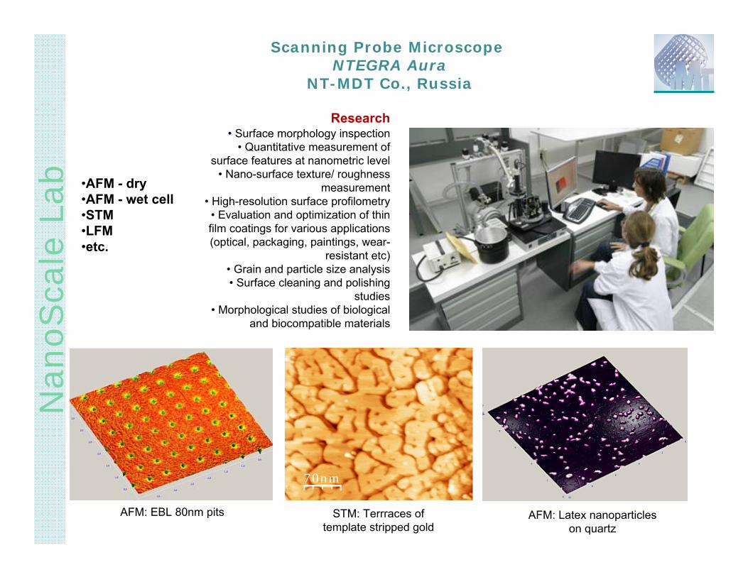
Scanning Probe MicroscopeNTEGRA Aura
NT-MDT Co., Russia
Nan
oSca
le L
ab •AFM - dry •AFM - wet cell •STM •LFM•etc.
Research • Surface morphology inspection
• Quantitative measurement of surface features at nanometric level
• Nano-surface texture/ roughness measurement
• High-resolution surface profilometry• Evaluation and optimization of thin film coatings for various applications (optical, packaging, paintings, wear-
resistant etc)• Grain and particle size analysis• Surface cleaning and polishing
studies• Morphological studies of biological
and biocompatible materials
70nm
AFM: EBL 80nm pits STM: Terrraces of template stripped gold
AFM: Latex nanoparticles on quartz

Nanomechanical Characterization equipmentNano Indenter G200
Agilent Technologies, USA
Nan
oSca
le L
ab
Research•High resolution mechanical
characterization of a wide variety of materials in small
volumes, thin films and coatings:-metals,
-semiconductors-ceramics
-biocompatible material.
•Determine: -hardness,
-film adherence-wear behaviour, etc.
Al indentation study

MIM
OM
EM
S lab
s
► Vector Network Analyzer (VNA) up to 110 GHz and on wafer measurement facilities in order to upgrade the 0.8-65 GHz existing on wafer characterization system
► Frequency synthesiser up to 65GHz
► Au plating facility for semiconductor wafers
►White light interferometer- optical profiling system for research applications
►Near field scanning optical microscope (SNOM)
Equipments acquired in the MIMOMEMS project
MIMOMEMS

MIM
OM
EM
S lab
s
Operating Modes:Near-field microscopy: transmission,
reflection, collection, fluorescenceConfocal microscopy: transmission,
reflection, fluorescence, can be upgraded with a Raman spectrometer
Atomic Force Microscopy contact and AC-Mode
Applications:- Imaging the optical properties of a
sample with resolution below the diffraction limit with applications in nanotechnology, nanophotonics, nanooptics and plasmonics
- Life sciences- Materials research- Single molecule detection.
Scanning Near-field Optical Microscope alpha 300S
Witec, Germany
Nanostructure characterization by near field scanning optical microscopy: a) transmission mode image of a hexagonal array of aluminium regions deposited on a glass substrate (Fisher pattern). b) reflection mode image of an array of polymer stripes realized by electron beam lithography.
Cooperation examples:• MIMOMEMS-REGPOT-FP7• FLEXPAET-IP- FP7/NMP

XRD
lab
X-ray Diffraction System (triple axis rotating anode) SmartLab
Rigaku Corporation, JapanTechnical characteristics:
9kW rotating anode, 200mm wafer
Triple axis, vertical goniometer
Independent Theta - Theta rotation
Horizontal sample position; X-Y Micro Area Mapping
XX-- Ray methods and applications for structural Analysis:Ray methods and applications for structural Analysis:
X-ray Powder diffraction (XRPD)High resolution X-ray diffraction (HRXRD) - phase
analysis, crystal orientation, thermal stability
X-ray reflectometry (XRR, including HRMR XRR ) - layer
thickness, density, roughness, interface layers;
Grazing incidence diffraction (GIXRD) -texture analysis and pole figures
In-plane grazing incidence diffraction (IPGID)Small angle X-ray scattering (SAXS)Single crystal diffraction (SCD)
Investigation of the
CH3(CH2)17SiCl3organic film monolayer

XRD
lab
SmartLab
Investigation of IMT-
optimized Au 111
deposition
0 30 60 90 120 150 1801e+4
1e+6
Aver
age
Inte
nsity
Cut Line
0 90 180 270 360Beta
1e+4
1e+6
Aver
age
Inte
nsity
Cut Circle

RAM
AN
lab
High Resolution Raman Spectrometer LabRAM HR 800
HORIBA Jobin Yvon, Japan
composition and phase (crystalline/amorphous) of
composites materials;
nature of oxides on compound semiconductors;
polymers characterizations and polimer
nanocomposites;
chemical and biological detection using SERS
technique;
micro/nano structures characterization -
micro/nanorods, carbon nanotubes (CNT), self
self assembled molecule (SAM) on functionalized
substrate for nano- bio applications
μμ-- Raman investigations of micro/nano Raman investigations of micro/nano structuresstructures

Nan
oBio
Lab
Micro-Nano PlotterOmniGrid
Genomic Solutions Ltd., UK
Nanobiotechnology laboratory: NanoBioLab
Au/PS samplesafter BSA printing - SEM
Dip and spot a given volume of sample solution
onto a solid surface
Print speed:10,000 spots/11 slides in
less than 3.5 hr
Vacuum wash station for washing between sample
transfers; humidity control minimizes sample
evaporation
Microarray sample
Cooperation example:•DNASIP-ERA-NET- focused
diagnostic DNA chips

Nan
oBio
Lab
Scanning Electrochemical MicroscopeElProScan
HEKA, Germany• Positioning system with 3 stepper motors (XY - 100 nm or 15 nm stepper motors) and a piezo translator
(5 nm resolution and 100 mm scan range, closed loop regulated) mounted on a granite portal including
fundamental plate
• Bipotentiostat/Galvanostat PG 340 with two low current Preamplifiers
• Software POTPULSE with SCAN extension
Applications:• Constant - distance Nano-SECM → Substrate imaging (Topography);
• Temperature-Controlled SECM;
• SECM for local corrosion investigation;
• Chemical reactivity → Heterogeneous electron transfer reactions studies; Electrocatalysis
• Probing patterned biological systems
• Bio SECM - Membrane transport
Directly measuring of the catalytic activity
of biosensor microelectrode arraysPrinciple of detection

Nan
oBio
Lab
Combined Time Resolved and Steady State Fluorescence Spectrometer - FLS920P - Edinburgh Instruments, UK
Zeta Potential and Submicron Particle Size Analyzer - DelsaNano -Beckman Coulter, USA
Applications• Formulation / tableting• Final QC• Formulation stability• Research
– Virus, bacteria– protein applications (aggregation) – bio-nanoparticles– Lyposomes, lipids, polysaccharides– Colloid drug carrier systems– Parenteral and oral drugs– micelles
• Zeta potential of tablet surface
Applications: photophysics, photochemistry, biophysics and semiconductor. Biomedical field: study of enzymes, dynamics and structure of nucleic acids, protein folding and DNA sequencing.
Pharmaceutical : monitoring drug interactions.Materials physics: study nanostructures such as quantum wells
and quantum dots; characterisation of doping or impurity level in semiconductors.
010
110
210
0 2 4 6 8 10 12 14 16 18
4.50.0
-4.5
Cou
nts
Res
idua
ls
Time/nsFluorescence decay of BSA-Cy3

Rel
iabili
ty lab
Testing for reliability
Semiconductor Characterization System (DC) with Wafer Probing
Station - 4200SCS/C/-
- various modules- (Keithley Instruments, USA)
Mobile Thermal Airstream System - ThermoStream TP04300A-
8C3-11 (Temptronic, USA)
Damp heat Climatic chamber (Angelantoni, Italy)
Electrodynamic vibration system with thermal and electrical tests
- TV 55240/LS (TIRA, Germany)
Thermal shock chamber - TSE-11-A (Espec Europe, Germany)
Universal Ovens with electrical testing - UFB 400 (Memmert,
Germany)
Highly Accelerated Stress Test Chamber - temperature, humidity,
pressure, polarization - EHS-211M (Espec Europe, Germany)
Free Fall Shock Machine - 0707-20 (MRAD, USA)
CAD
/CAE/M
ultip
hys
ics
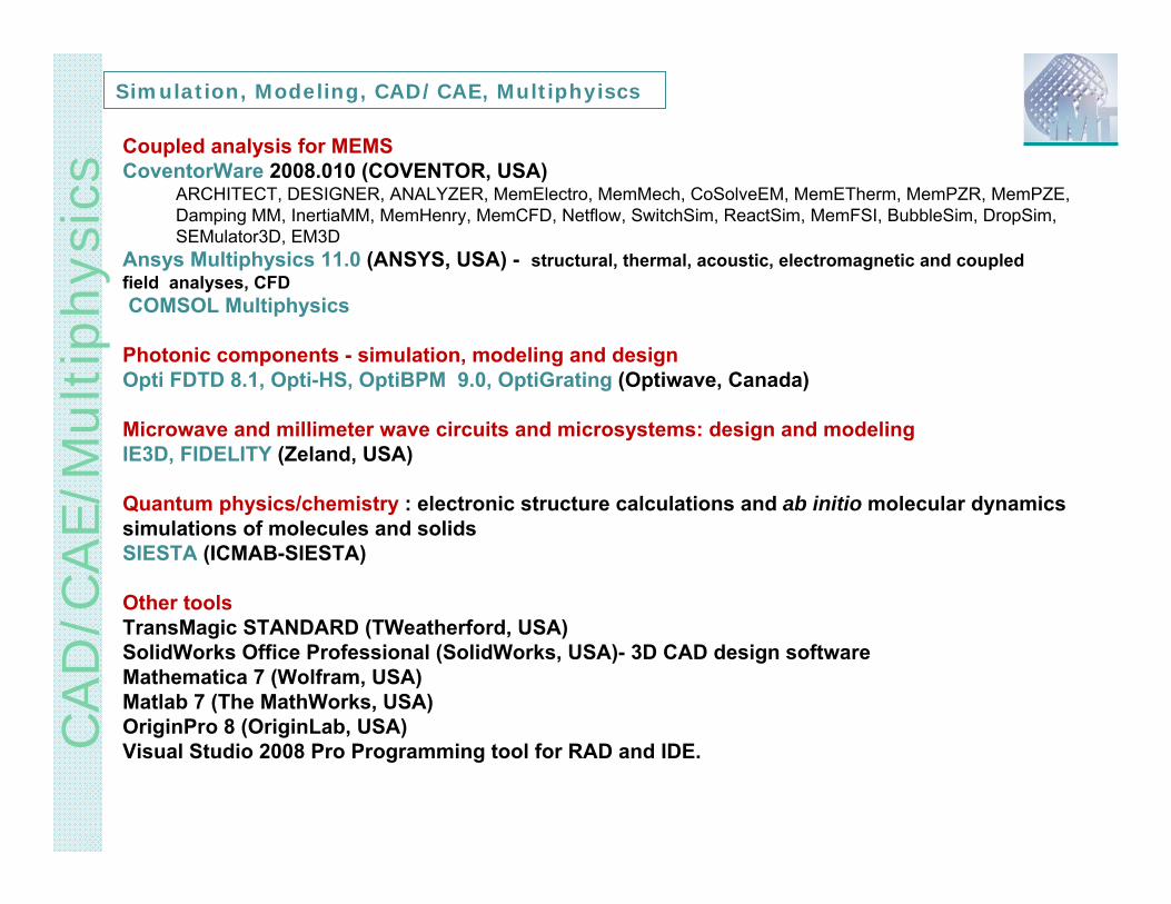
Simulation, Modeling, CAD/CAE, Multiphyiscs
Coupled analysis for MEMSCoventorWare 2008.010 (COVENTOR, USA)
ARCHITECT, DESIGNER, ANALYZER, MemElectro, MemMech, CoSolveEM, MemETherm, MemPZR, MemPZE, Damping MM, InertiaMM, MemHenry, MemCFD, Netflow, SwitchSim, ReactSim, MemFSI, BubbleSim, DropSim, SEMulator3D, EM3D
Ansys Multiphysics 11.0 (ANSYS, USA) - structural, thermal, acoustic, electromagnetic and coupled field analyses, CFDCOMSOL Multiphysics
Photonic components - simulation, modeling and design Opti FDTD 8.1, Opti-HS, OptiBPM 9.0, OptiGrating (Optiwave, Canada)
Microwave and millimeter wave circuits and microsystems: design and modelingIE3D, FIDELITY (Zeland, USA)
Quantum physics/chemistry : electronic structure calculations and ab initio molecular dynamics simulations of molecules and solidsSIESTA (ICMAB-SIESTA)
Other toolsTransMagic STANDARD (TWeatherford, USA) SolidWorks Office Professional (SolidWorks, USA)- 3D CAD design software Mathematica 7 (Wolfram, USA) Matlab 7 (The MathWorks, USA) OriginPro 8 (OriginLab, USA) Visual Studio 2008 Pro Programming tool for RAD and IDE.

CAD
/CAE/M
ultip
hys
ics
MI-Lab-on-Chip - FP6 STREP/NMP
MEMSAS - CEEX
Capacitive microphone optimization
Si microreflector optimization
Micromanipulation element (microgripper)
First principles electronic structure calculations
LoC for molecular imaging agents

Colla
bora
tion a
nd p
ersp
ective
s Collaboration matrix
Partnerships in RTD activities, sharing the IP resulting from research
Scientific and technological services, including design and consulting
Direct access, “hands-on” activities (after proper training)
Research groups outside IMT-Bucharest
- usually financed by a contract of partnership agreement.
- typically, specific activities will be performed by IMT-Bucharest as a subcontractor (technological processes, analysis and characterization, design and simulation, etc.) with no IP rights.
- direct access of researchers from partner organizations, as part of common RTD.
Educational bodies for Ph.D. and postdoctoral studies, M.Sc. studies, “hands-on” training etc.
- supported by individual grants or following an agreement with universities, specifying the cost and intellectual property issues.
- occasionally.
- as part of a common research activity, or providing training on a commercial basis.
Companies(Industry)
- based on special NDA and IP agreements.
- services provided on commercial basis.
- companies may use their own IP rights.

IMT-MINAFAB full info -www.imt.ro/MINAFAB/
Current projects and achievements: IMT-Bucharest - SCIENTIFIC REPORT 2008 -www.imt.ro/raport_anual_2008.pdf (soon available for 2009)
IMT-Bucharest - Brochure for scientific-technological services -www.imt.ro/brosura_imt_bucuresti_2009.pdf
Quick list of capabilities and tools -http://www.imt.ro/MINAFAB/description.htm
Complete information
Thank you for your attention!Thank you for your attention!