Embed Size (px)
Citation preview

GS-EVB-IMS3-665xxB-GS High Power IMS3 Evaluation Platform
Technical Manual _____________________________________________________________________________________________________________________
GS-EVB-IMS3-665xxB-GS TM Rev. 201207 © 2020 GaN Systems Inc www.gansystems.com 1 Please refer to the Evaluation Board/Kit Important Notice on page 21
GS-EVB-IMS3-665xxB-GS GS-EVB-IMS3-66508B-GS GS-EVB-IMS3-66516B-GS High Power IMS 3 Evaluation Platform
Technical Manual
Visit www.gansystems.com for the latest version of this technical manual.

GS-EVB-IMS3-665xxB-GS High Power IMS3 Evaluation Platform
Technical Manual _____________________________________________________________________________________________________________________
GS-EVB-IMS3-665xxB-GS TM Rev. 201207 © 2020 GaN Systems Inc www.gansystems.com 2 Please refer to the Evaluation Board/Kit Important Notice on page 21
DANGER DO NOT TOUCH THE BOARD WHEN IT IS ENERGIZED AND ALLOW ALL COMPONENTS TO DISCHARGE COMPLETELY PRIOR HANDLING THE BOARD. HIGH VOLTAGE CAN BE EXPOSED ON THE BOARD WHEN IT IS CONNECTED TO POWER SOURCE. EVEN BRIEF CONTACT DURING OPERATION MAY RESULT IN SEVERE INJURY OR DEATH. Please sure that appropriate safety procedures are followed. This evaluation kit is designed for engineering evaluation in a controlled lab environment and should be handled by qualified personnel ONLY. Never leave the board operating unattended. WARNING Some components can be hot during and after operation. There is NO built-in electrical or thermal protection on this evaluation kit. The operating voltage, current, and component temperature should be monitored closely during operation to prevent device damage. CAUTION This product contains parts that are susceptible to damage by electrostatic discharge (ESD). Always follow ESD prevention procedures when handling the product.

GS-EVB-IMS3-665xxB-GS High Power IMS3 Evaluation Platform
Technical Manual _____________________________________________________________________________________________________________________
GS-EVB-IMS3-665xxB-GS TM Rev. 201207 © 2020 GaN Systems Inc www.gansystems.com 3 Please refer to the Evaluation Board/Kit Important Notice on page 21
Contents 1 Overview .............................................................................................................................................................. 5
1.1 Introduction ............................................................................................................................................... 5
1.2 Features and Benefits ................................................................................................................................ 5
1.3 Applications ............................................................................................................................................... 5
1.4 Contents ...................................................................................................................................................... 5
2 Technical Specifications of IMS 3 Half Bridge Daughter Power Board....................................................... 7
2.1 On‐board GaN E‐mode Transistors ........................................................................................................ 7
2.2 IMS3 Board Thermal Design .................................................................................................................... 7
2.3 IMS3 Half Bridge Board Design ............................................................................................................ 10
3 Compatible Driver Motherboard Options..................................................................................................... 11
4 Operation Modes .............................................................................................................................................. 13
5 Test Results ........................................................................................................................................................ 15
5.1 Double Pulse Test (GS‐EVB‐HBDB‐IMS + GS‐EVB‐IMS3‐66508B‐GS) ............................................ 15
5.2 Boost Configuration Test (GS‐EVB‐HBDB‐IMS + GS‐EVB‐IMS3‐66508B‐GS) ................................ 17
6 GS‐EVB‐IMS3‐665xxB‐GS Schematics and BoM ........................................................................................... 19

GS-EVB-IMS3-665xxB-GS High Power IMS3 Evaluation Platform
Technical Manual _____________________________________________________________________________________________________________________
GS-EVB-IMS3-665xxB-GS TM Rev. 201207 © 2020 GaN Systems Inc www.gansystems.com 4 Please refer to the Evaluation Board/Kit Important Notice on page 21
List of Figures
Figure 1 IMS3 daughter power boards with heatsinks ........................................................................................ 5
Figure 2 GS66516B and GS66508B GaNPX® packaged GaN E‐mode transistors ............................................ 7
Figure 3 Cross‐section view of a single layer IMS3 board ................................................................................... 8
Figure 4 Comparison of junction to heatsink thermal resistance (RthJ‐HS) (Estimated based on GS66516B) .. 9
Figure 5 IMS3 half‐bridge daughter power board (GS‐EVB‐IMS3‐66508B‐GS) .............................................. 10
Figure 6 Compatible driver motherboards .......................................................................................................... 11
Figure 7 Double pulse test setup schematics ....................................................................................................... 15
Figure 8 Double pulse test setup ........................................................................................................................... 15
Figure 9 Double pulse test waveforms (400V/30A) ............................................................................................. 16
Figure 10 Boost configuration test setup schematics .......................................................................................... 17
Figure 11 Boost configuration test setup .............................................................................................................. 17
Figure 12 Boost configuration test thermal measurement result ...................................................................... 18
Figure 13 Test waveforms (400Vin, 10kHz, Po=0.8kW) ...................................................................................... 18
List of Tables Table 1 GS‐EVB‐IMS3‐665xxB‐GS Evaluation Kit Contents ................................................................................. 5
Table 2 IMS3 daughter power board part numbers and description .................................................................. 6
Table 3 Performance comparison of 2 thermal design options for SMT power devices ................................... 8
Table 4 Compatible driver motherboards for IMS3 daughter power board GS‐EVB‐IMS3‐665XXB ............ 11
Table 5 Driver motherboard part numbers and description .............................................................................. 12
Table 6 Half bridge configurations operation mode using GS‐EVB‐HBDB‐IMS ............................................. 13
Table 7 dual half bridge/full bridge configurations operation mode using GSP665HPMB‐EVBIMS2 ......... 14

GS-EVB-IMS3-665xxB-GS High Power IMS3 Evaluation Platform
Technical Manual _____________________________________________________________________________________________________________________
GS-EVB-IMS3-665xxB-GS TM Rev. 201207 © 2020 GaN Systems Inc www.gansystems.com 5 Please refer to the Evaluation Board/Kit Important Notice on page 21
1 Overview
1.1 Introduction
This horizontal Insulated Metal Substrate (IMS3) evaluation platform can be used to evaluate the electrical
and thermal performance benefits of GaNPX® bottom‐side cooled E‐modes in high power applications.
The optimized thermal and electrical designs provide an excellent reference for implementing a low cost,
high performance design.
1.2 Features and Benefits
• Improved heat transfer
• Increased power density
• Reduced system cost
• High thermal conductivity (7.0 W/mK)
1.3 Applications
• Automotive: 3.3kW‐22kW on board charger, DC/DC, 3‐Φ inverter, high power wireless charger
• Industrial: 3‐7kW Photovoltaic Inverter and Energy Storage System (ESS), Motor Drive / VFD
• Server/Datacenter: 3kW Server ACDC power supply.
• Consumer: Residential Energy Storage System (ESS)
1.4 Contents
As referred to Figure 1, the GS-EVB-IMS3-665xxB-GS includes the following hardware in Table 1:
Table 1 GS-EVB-IMS3-665xxB-GS Evaluation Kit Contents
Quantity Description
1 GS‐EVB‐IMS3‐66508B 3 kW Half Bridge Daughter Power Board
1 GS‐EVB‐IMS3‐66516B 6 kW Half Bridge Daughter Power Board
Figure 1 IMS3 daughter power boards with heatsinks

GS-EVB-IMS3-665xxB-GS High Power IMS3 Evaluation Platform
Technical Manual _____________________________________________________________________________________________________________________
GS-EVB-IMS3-665xxB-GS TM Rev. 201207 © 2020 GaN Systems Inc www.gansystems.com 6 Please refer to the Evaluation Board/Kit Important Notice on page 21
A suitable heatsink is included for lower power applications. For higher power applications additional
heatsinking may be required. To prevent device damage, ensure adequate heatsinking through design and
by monitoring the component temperatures during operation.
To assemble a heatsink, apply thermal grease to the heatsink / IMS board interface before screwing the
units together. Enough thermal grease should be applied so that a small amount extrudes on all four sizes
as the screws are tightened. Wipe the assembly clean.
The ordering information is listed in Table 2 below:
Table 2 IMS3 daughter power board part numbers and description
PART NUMBER DESCRIPTION POWER
LEVEL GaN E‐mode
GS‐EVB‐IMS3‐66508B 650 V GaN High Power IMS3 Half Bridge 3 kW GS66508B
GS‐EVB‐IMS3‐66516B 650 V GaN High Power IMS3 Half Bridge 6 kW GS66516B

GS-EVB-IMS3-665xxB-GS High Power IMS3 Evaluation Platform
Technical Manual _____________________________________________________________________________________________________________________
GS-EVB-IMS3-665xxB-GS TM Rev. 201207 © 2020 GaN Systems Inc www.gansystems.com 7 Please refer to the Evaluation Board/Kit Important Notice on page 21
2 Technical Specifications of IMS 3 Half Bridge Daughter Power Board 2.1 On-board GaN E-mode Transistors
Using this platform, power designers can evaluate the performance of GaN Systems’ E‐mode transistors in
high power, high‐efficiency applications. The IMS3 half‐bridge daughter power board is populated with
GaN Systems’ GS66516B (bottom‐side cooled GaN E‐mode transistor, rated at 650 V / 25 mΩ) or GS66508B
(bottom‐side cooled GaN E‐mode transistor, rated at 650 V / 50 mΩ), as shown in Figure 2. The embedded
GaNPX® SMD package has the following features:
Large power source/thermal pad for improved thermal dissipation.
Bottom‐side cooled packaging for conventional PCB or advanced IMS/Cu inlay thermal design.
Ultra‐low inductance for high‐frequency switching.
Figure 2 GS66516B and GS66508B GaNPX® packaged GaN E-mode transistors
The IMS3 half‐bridge daughter power board is designed for users to gain hands‐on experience in the
following ways:
Evaluate the GaN E‐mode transistors performance in any half‐bridge‐based topology, over
a range of operating conditions.
Use as a thermal and electrical design reference of the GS66516B or GS66508B GaNPX®
package in demanding high‐power and high‐efficiency applications.
2.2 IMS3 Board Thermal Design
An IMS3 power daughter board assembly uses metal as the PCB core, to which a dielectric layer and copper
foil layers are bonded, as shown in Figure 3. The metal PCB core is often aluminum. The copper foil layers
can be single or double‐sided. An IMS3 board offers superior thermal conductivity to standard FR4 PCB.
It’s commonly used in high‐power, high current applications where most of the heat is concentrated in a
small footprint SMT device.
As high‐speed Gallium Nitride power devices are adopted widely, the industry is trending away from
through‐hole packaging (TH), towards surface‐mount packaging (SMT). Traditional TH devices, such as
the TO‐220, are no longer the appropriate choice because their high parasitic inductance and capacitance
negate the performance benefits offered by GaN E‐mode transistors. SMT packaging, such as PQFN,
D2PAK, and GaN Systems’ GaNPX®, by comparison, offer low inductance and low thermal impedance,
enabling efficient designs at high power and high switching frequency.

GS-EVB-IMS3-665xxB-GS High Power IMS3 Evaluation Platform
Technical Manual _____________________________________________________________________________________________________________________
GS-EVB-IMS3-665xxB-GS TM Rev. 201207 © 2020 GaN Systems Inc www.gansystems.com 8 Please refer to the Evaluation Board/Kit Important Notice on page 21
Figure 3 Cross-section view of a single layer IMS3 board
Thermal management of SMT power transistors must be approached differently than TH devices. TO
packages are cooled by attaching them to a heatsink, with an intermediary Thermal Interface Material (TIM)
sheet for electrical high voltage insulation. The traditional cooling method for SMT power devices is to use
thermal vias tied to multiple copper layers in a PCB. The IMS3 board presents designers with another
option which is especially useful for high power applications. The IMS 3 board has a much lower junction
to heatsink thermal resistance (RthJ‐HS) than FR4 PCBs, for efficient heat transfer out of the transistor. As
well, assembly on an IMS3 board has lower assembly cost and risk than the TH alternative. The manual
assembly process of a TO package onto a heatsink is costly and prone to human error.
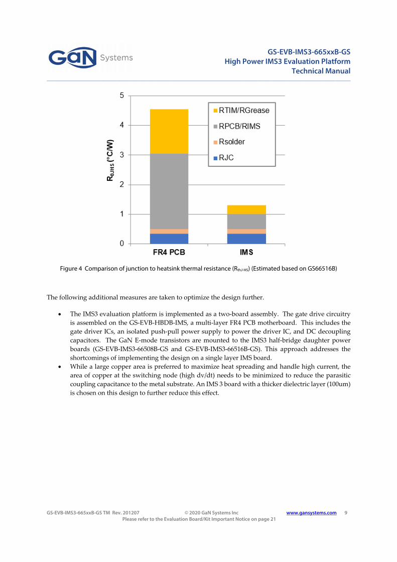
Table 3 compares 2 different design approaches for cooling discrete SMT power devices. While the cost is
lower for an FR4 PCB cooling with thermal vias, the IMS 3 board offers the best performance for thermal
management. Figure 4 provides a quantitative comparison of the thermal resistance for the 2 design
options. The IMS3 board clearly comes out ahead.
Table 3 Performance comparison of 2 thermal design options for SMT power devices
IMS PCB
Thermal grease
IMS Board
Thermal resistance Good Best
Electrical Insulation
Use TIM Yes
Cost Lowest Low
Advantages Standard process Layout flexibility
Electrically isolated
Design challenges High PCB thermal resistance
Usually layout limited to 1 layer Parasitic inductance
Coupling capacitances to the metal substrate
FR4 PCB Cooling with Vias
TIM
GS-EVB-IMS3-665xxB-GS High Power IMS3 Evaluation Platform
Technical Manual _____________________________________________________________________________________________________________________
GS-EVB-IMS3-665xxB-GS TM Rev. 201207 © 2020 GaN Systems Inc www.gansystems.com 9 Please refer to the Evaluation Board/Kit Important Notice on page 21
Figure 4 Comparison of junction to heatsink thermal resistance (RthJ-HS) (Estimated based on GS66516B)
The following additional measures are taken to optimize the design further.
The IMS3 evaluation platform is implemented as a two‐board assembly. The gate drive circuitry
is assembled on the GS‐EVB‐HBDB‐IMS, a multi‐layer FR4 PCB motherboard. This includes the
gate driver ICs, an isolated push‐pull power supply to power the driver IC, and DC decoupling
capacitors. The GaN E‐mode transistors are mounted to the IMS3 half‐bridge daughter power
boards (GS‐EVB‐IMS3‐66508B‐GS and GS‐EVB‐IMS3‐66516B‐GS). This approach addresses the
shortcomings of implementing the design on a single layer IMS board.
While a large copper area is preferred to maximize heat spreading and handle high current, the
area of copper at the switching node (high dv/dt) needs to be minimized to reduce the parasitic
coupling capacitance to the metal substrate. An IMS 3 board with a thicker dielectric layer (100um)
is chosen on this design to further reduce this effect.

GS-EVB-IMS3-665xxB-GS High Power IMS3 Evaluation Platform
Technical Manual _____________________________________________________________________________________________________________________
GS-EVB-IMS3-665xxB-GS TM Rev. 201207 © 2020 GaN Systems Inc www.gansystems.com 10 Please refer to the Evaluation Board/Kit Important Notice on page 21
2.3 IMS3 Half Bridge Board Design
Figure 5 IMS3 half-bridge daughter power board (GS-EVB-IMS3-66508B-GS)
The IMS3 half‐bridge daughter power board is populated with the following components:
Q1 and Q2: GS66516B or GS66508B in a half‐bridge configuration.
o 6kW GS‐EVB‐IMS3‐66516B‐GS: Q1/Q2 GS66516B.
o 3kW GS‐EVB‐IMS3‐66508B‐GS: Q1/Q2 GS66508B.
J1, J2, J3:
o Connector Header Surface Mount 12 position 0.050ʺ (1.27mm) (Samtec Inc., P/N: FTS‐106‐
02‐F‐DV).
o These terminals are designed to carry the main current and gate signals.
GS-EVB-IMS3-665xxB-GS High Power IMS3 Evaluation Platform
Technical Manual _____________________________________________________________________________________________________________________
GS-EVB-IMS3-665xxB-GS TM Rev. 201207 © 2020 GaN Systems Inc www.gansystems.com 11 Please refer to the Evaluation Board/Kit Important Notice on page 21
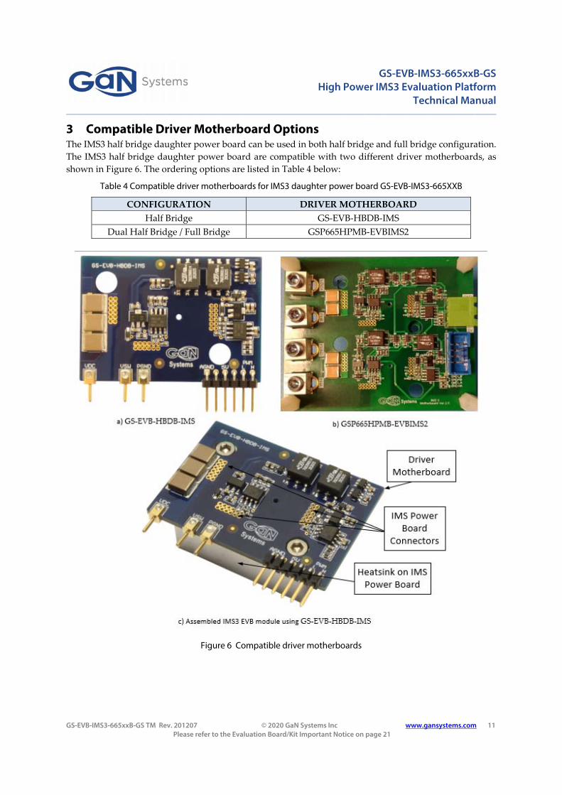
3 Compatible Driver Motherboard Options The IMS3 half bridge daughter power board can be used in both half bridge and full bridge configuration.
The IMS3 half bridge daughter power board are compatible with two different driver motherboards, as
shown in Figure 6. The ordering options are listed in Table 4 below:
Table 4 Compatible driver motherboards for IMS3 daughter power board GS-EVB-IMS3-665XXB
CONFIGURATION DRIVER MOTHERBOARD
Half Bridge GS‐EVB‐HBDB‐IMS
Dual Half Bridge / Full Bridge GSP665HPMB‐EVBIMS2
Figure 6 Compatible driver motherboards

GS-EVB-IMS3-665xxB-GS High Power IMS3 Evaluation Platform
Technical Manual _____________________________________________________________________________________________________________________
GS-EVB-IMS3-665xxB-GS TM Rev. 201207 © 2020 GaN Systems Inc www.gansystems.com 12 Please refer to the Evaluation Board/Kit Important Notice on page 21
The ordering information are listed in Table 5 below:
Table 5 Driver motherboard part numbers and description
PART NUMBER DESCRIPTION
GS‐EVB‐HBDB‐IMS
650 V Universal Half Bridge Isolated Driver Motherboard for IMS2 &
IMS3
GSP665HPMB‐EVBIMS2 650 V Universal High‐Power Dual Half Bridge / Full Bridge Driver
Motherboard for IMS2 & IMS3
For more information related to the driver mother boards about their:
Features and Benefits
Applications
Technical Specifications (design overview, gate driver circuit, 5V input and external PWM signals
input, temperature monitoring hole, installation of IMS half‐bridge daughter power board, and DC
link decoupling capacitors)
Schematics and BoM
please refer to driver mother boards technical manuals on https://gansystems.com/evaluation‐boards/

GS-EVB-IMS3-665xxB-GS High Power IMS3 Evaluation Platform
Technical Manual _____________________________________________________________________________________________________________________
GS-EVB-IMS3-665xxB-GS TM Rev. 201207 © 2020 GaN Systems Inc www.gansystems.com 13 Please refer to the Evaluation Board/Kit Important Notice on page 21
4 Operation Modes The IMS3 EVB half‐bridge daughter power boards can be configured into different topologies and
operation modes with the two driver motherboards, as shown below:
Table 6 Half bridge configurations operation mode using GS-EVB-HBDB-IMS
Double Pulse Test Half Bridge LLC
Synchronous Buck DC/DC Single Phase Half Bridge Inverter
Synchronous Boost DC/DC Totem Pole PFC

GS-EVB-IMS3-665xxB-GS High Power IMS3 Evaluation Platform
Technical Manual _____________________________________________________________________________________________________________________
GS-EVB-IMS3-665xxB-GS TM Rev. 201207 © 2020 GaN Systems Inc www.gansystems.com 14 Please refer to the Evaluation Board/Kit Important Notice on page 21
Table 7 dual half bridge/full bridge configurations operation mode using GSP665HPMB-EVBIMS2
HALF BRIDGE FULL BRIDGE BOOST MODE
Double Pulse Test Full Bridge LLC Synchronous Boost DC/DC
Gate Driver
DC Power Source
Vdc+
Vdc‐
PHA
PHB
Vdc+
PGND
COCr
RL
Lr
Gate Driver
Vdc+
PHA
PHB
Vdc+
PGND
L
CDC Power Source
RL
PGND
Synchronous Buck DC/DC Phase Shift Full Bridge Totem Pole PFC
Gate Driver
DC Power Source
Vdc+
Vdc‐
PHA
PHB
Vdc+
PGND
L
C RL
Gate Driver
DC Power Source
Vdc+
Vdc‐
PHA
PHB
Vdc+
PGND
CORL
Lr
LO
Gate Driver
Vdc+
PHA
PHB
Vdc+
PGND
L
AC Power Source
RL
PGND
Half Bridge LLC Full Bridge Inverter Interleaved Totem Pole PFC
Gate Driver
DC Power Source
Vdc+
Vdc‐
PHA
PHB
Vdc+
PGND
COCr
RL
Lr
Gate Driver
DC Power Source
Vdc+
Vdc‐
PHA
PHB
Vdc+
PGND
CORL
LO
Gate Driver
Vdc+
PHA
PHB
Vdc+
PGND
L1 AC Power Source
RL
PGND
L2
Single Phase Half Bridge Inverter DUAL ACTIVE BRIDGE
Gate Driver
DC Power Source
Vdc+
Vdc‐
PHA
PHB
Vdc+
PGND
CORL
LO
Dual Active Bridge (with 2 mother boards)
Gate Driver
DC Power Source
Vdc+
Vdc‐
PHA
PHB
Vdc+
PGND
Lr
Gate Driver
Vdc+
PHA
PHB
Vdc+
PGND
RL
Gate Driver
DC Power Source
Vdc+
Vdc‐
PHA
PHB
Vdc+
PGND

GS-EVB-IMS3-665xxB-GS High Power IMS3 Evaluation Platform
Technical Manual _____________________________________________________________________________________________________________________
GS-EVB-IMS3-665xxB-GS TM Rev. 201207 © 2020 GaN Systems Inc www.gansystems.com 15 Please refer to the Evaluation Board/Kit Important Notice on page 21
5 Test Results 5.1 Double Pulse Test (GS-EVB-HBDB-IMS + GS-EVB-IMS3-66508B-GS)
Test condition: VDS = 400V, ID = 30A, VGS = +6V/‐3V, L = 37uH, No RC Snubber, TJ =25℃ Measured peak VDS = 630V and 92 V/ns peak dV/dt
Reliable hard switching with GS66508B is achieved at full rated current
Figure 7 Double pulse test setup schematics
Figure 8 Double pulse test setup

GS-EVB-IMS3-665xxB-GS High Power IMS3 Evaluation Platform
Technical Manual _____________________________________________________________________________________________________________________
GS-EVB-IMS3-665xxB-GS TM Rev. 201207 © 2020 GaN Systems Inc www.gansystems.com 16 Please refer to the Evaluation Board/Kit Important Notice on page 21
Figure 9 Double pulse test waveforms (400V/30A)

GS-EVB-IMS3-665xxB-GS High Power IMS3 Evaluation Platform
Technical Manual _____________________________________________________________________________________________________________________
GS-EVB-IMS3-665xxB-GS TM Rev. 201207 © 2020 GaN Systems Inc www.gansystems.com 17 Please refer to the Evaluation Board/Kit Important Notice on page 21
5.2 Boost Configuration Test (GS-EVB-HBDB-IMS + GS-EVB-IMS3-66508B-GS)
Test condition: VIN = 400V, fsw=10kHz, Po=0.8kW, TAMB = 25℃. Device case temperature 72℃
Figure 10 Boost configuration test setup schematics
Figure 11 Boost configuration test setup

GS-EVB-IMS3-665xxB-GS High Power IMS3 Evaluation Platform
Technical Manual _____________________________________________________________________________________________________________________
GS-EVB-IMS3-665xxB-GS TM Rev. 201207 © 2020 GaN Systems Inc www.gansystems.com 18 Please refer to the Evaluation Board/Kit Important Notice on page 21
Figure 12 Boost configuration test thermal measurement result
Figure 13 Test waveforms (400Vin, 10kHz, Po=0.8kW)
Ch#1 (blue): Drain‐source voltage, 100V/div
Ch#4 (green): Inductor current, 5A/div

GS-EVB-IMS3-665xxB-GS High Power IMS3 Evaluation Platform
Technical Manual _____________________________________________________________________________________________________________________
GS-EVB-IMS3-665xxB-GS TM Rev. 201207 © 2020 GaN Systems Inc www.gansystems.com 19 Please refer to the Evaluation Board/Kit Important Notice on page 21
6 GS-EVB-IMS3-665xxB-GS Schematics and BoM
GS-EVB-IMS3-66508B-GS assembly drawing GS-EVB-IMS3-66516B-GS assembly drawing

GS-EVB-IMS3-665xxB-GS High Power IMS3 Evaluation Platform
Technical Manual _____________________________________________________________________________________________________________________
GS-EVB-IMS3-665xxB-GS TM Rev. 201207 © 2020 GaN Systems Inc www.gansystems.com 20 Please refer to the Evaluation Board/Kit Important Notice on page 21
GS-EVB-IMS3-66508B-GS PCB layout GS-EVB-IMS3-66516B-GS PCB layout
Bill of Materials (BOM)

GS-EVB-IMS3-665xxB-GS High Power IMS 3 Evaluation Platform
Technical Manual ___________________________________________________________________________________________________________________
GS-EVB-IMS3-665xxB-GS TM Rev. 201207 © 2020 GaN Systems Inc. www.gansystems.com 21
Please refer to the Evaluation Board/Kit Important Notice on page 21
Evaluation Board/kit Important Notice
GaN Systems Inc. (GaN Systems) provides the enclosed product(s) under the following AS IS conditions:
This evaluation board/kit being sold or provided by GaN Systems is intended for use for ENGINEERING
DEVELOPMENT, DEMONSTRATION, and OR EVALUATION PURPOSES ONLY and is not considered by GaN
Systems to be a finished end‐product fit for general consumer use. As such, the goods being sold or provided are
not intended to be complete in terms of required design‐, marketing‐, and/or manufacturing‐related protective
considerations, including but not limited to product safety and environmental measures typically found in end
products that incorporate such semiconductor components or circuit boards. This evaluation board/kit does not fall
within the scope of the European Union directives regarding electromagnetic compatibility, restricted substances
(RoHS), recycling (WEEE), FCC, CE or UL, and therefore may not meet the technical requirements of these directives,
or other related regulations.
If this evaluation board/kit does not meet the specifications indicated in the Technical Manual, the board/kit may be
returned within 30 days from the date of delivery for a full refund. THE FOREGOING WARRANTY IS THE
EXCLUSIVE WARRANTY MADE BY THE SELLER TO BUYER AND IS IN LIEU OF ALL OTHER WARRANTIES,
EXPRESSED, IMPLIED, OR STATUTORY, INCLUDING ANY WARRANTY OF MERCHANTABILITY OR FITNESS
FOR ANY PARTICULAR PURPOSE. EXCEPT TO THE EXTENT OF THIS INDEMNITY, NEITHER PARTY SHALL
BE LIABLE TO THE OTHER FOR ANY INDIRECT, SPECIAL, INCIDENTAL, OR CONSEQUENTIAL DAMAGES.
The user assumes all responsibility and liability for proper and safe handling of the goods. Further, the user
indemnifies GaN Systems from all claims arising from the handling or use of the goods. Due to the open construction
of the product, it is the user’s responsibility to take any and all appropriate precautions with regard to electrostatic
discharge.
No License is granted under any patent right or other intellectual property right of GaN Systems whatsoever. GaN
Systems assumes no liability for applications assistance, customer product design, software performance, or
infringement of patents or any other intellectual property rights of any kind.
GaN Systems currently services a variety of customers for products around the world, and therefore this transaction
is not exclusive.
Please read the Technical Manual and, specifically, the Warnings and Restrictions notice in the Technical Manual
prior to handling the product. Persons handling the product(s) must have electronics training and observe good
engineering practice standards.
This notice contains important safety information about temperatures and voltages. For further safety concerns,
please contact a GaN Systems’ application engineer.

GS-EVB-IMS3-665xxB-GS High Power IMS 3 Evaluation Platform
Technical Manual ___________________________________________________________________________________________________________________
GS-EVB-IMS3-665xxB-GS TM Rev. 201207 © 2020 GaN Systems Inc. www.gansystems.com 22
Please refer to the Evaluation Board/Kit Important Notice on page 21
In Canada: GaN Systems Inc. 1145 Innovation Drive Suite 101 Ottawa, Ontario, Canada K2K 3G8 T +1 613-686-1996
In Europe: GaN Systems Ltd., German Branch Terminalstrasse Mitte 18, 85356 München, Germany T +49 (0) 8165 9822 7260
In the United States: GaN Systems Corp. 2723 South State Street, Suite 150, Ann Arbor, MI. USA 48104 T +1 248-609-7643
www.gansystems.com Important Notice – Unless expressly approved in writing by an authorized representative of GaN Systems, GaN Systems components are not designed, authorized or warranted for use in lifesaving, life sustaining, military, aircraft, or space applications, nor in products or systems where failure or malfunction may result in personal injury, death, or property or environmental damage. The information given in this document shall not in any event be regarded as a guarantee of performance. GaN Systems hereby disclaims any or all warranties and liabilities of any kind, including but not limited to warranties of non-infringement of intellectual property rights. All other brand and product names are trademarks or registered trademarks of their respective owners. Information provided herein is intended as a guide only and is subject to change without notice. The information contained herein or any use of such information does not grant, explicitly, or implicitly, to any party any patent rights, licenses, or any other intellectual property rights. General Sales and Terms Conditions apply. © 2009-2019 GaN Systems Inc. All rights reserved.


![[대학내일20대연구소]201207 대학생들이주로마시는음료구매와이용에대해(20120730)](https://img.dokumen.tips/doc/110x75/556298c6d8b42abb398b4e99/20201207-20120730.jpg)