Embed Size (px)
Citation preview

UNIVERSIDADE FEDERAL DO RIO GRANDE DO SULINSTITUTO DE INFORMÁTICA
PROGRAMA DE PÓS-GRADUAÇÃO EM MICROELETRÔNICA
PAULO CESAR SANTOS
Improving Efficiency ofGeneral Purpose Computer Systemsby adopting Processing-in-Memory
Architecture
Thesis presented in partial fulfillmentof the requirements for the degree ofDoctor of Microeletronics
Advisor: Prof. Dr. Antonio Carlos S. BeckCoadvisor: Prof. Dr. Marco Antônio Z. Alves
Porto AlegreJanuary 2020

CIP — CATALOGING-IN-PUBLICATION
Santos, Paulo Cesar
Improving Efficiency ofGeneral Purpose Computer Systemsby adopting Processing-in-Memory Architecture / Paulo CesarSantos. – Porto Alegre: PGMICRO da UFRGS, 2020.
117 f.: il.
Thesis (Ph.D.) – Universidade Federal do Rio Grande do Sul.Programa de Pós-Graduação em Microeletrônica, Porto Alegre,BR–RS, 2020. Advisor: Antonio Carlos S. Beck; Coadvisor:Marco Antônio Z. Alves.
1. Processing-in-memory. 2. 3D-stacked memory. 3. Perfor-mance efficiency. 4. Energy efficiency. 5. Area efficiency. 6. Codegeneration. 7. Compiler. I. Beck, Antonio Carlos S.. II. Alves,Marco Antônio Z.. III. Título.
UNIVERSIDADE FEDERAL DO RIO GRANDE DO SULReitor: Prof. Rui Vicente OppermannVice-Reitora: Profa. Jane Fraga TutikianPró-Reitor de Pós-Graduação: Prof. Celso Giannetti Loureiro ChavesDiretora do Instituto de Informática: Profa. Carla Maria Dal Sasso FreitasCoordenadora do PGMICRO: Prof. Fernanda Gusmão de Lima KastensmidtBibliotecária-chefe do Instituto de Informática: Beatriz Regina Bastos Haro


ABSTRACT
For decades the inherent limitations of traditional Von Neumann-based computer sys-
tems have been overshadowed by the fine-grain architectural advancements and the ever-
increasing technological evolution. However, in the last years, the technological advance
has been slower, and at the current pace, the technology has contributed less and less to
the performance of modern systems. In this way, a new era arises demanding disruptive
architectural approaches, either in the creation of new architectures or in the way in which
the existing ones are used. Supported by 3D-stacking technologies that allow integration of
memory and logic, new opportunities to revive old techniques have emerged. One of these
is Processing-in-Memory (PIM), which provides resources for computing data directly
in memory. This thesis takes advantage of these new opportunities by developing a PIM
design targeting to mitigate the current architectures limitations. Although disruptive in the
sense of performance, efficiency and programmability, the presented approach intends to
be general-purpose friendly. However, several challenges must be overpassed to allow PIM
adoption. Moreover, these challenges are burdensome when the goal consists of overcom-
ing current general-purpose architectures deficiencies, and allowing the use of PIM as part
of a general-purpose environment. The design shown in this thesis allows to improve the
overall performance and energy efficiency of the general-purpose systems by adopting the
Reconfigurable Vector Unit (RVU) architecture, while providing Processing-In-Memory
cOmpiler (PRIMO), a complete tool set that automatically exploits the available PIM
resources. The RVU PIM approach can outperform the current General Purpose Processors
(GPPs) by achieving theoretically 2 TFLOPS. Also, the proposed PIM exceeds the ARM
processors’ power efficiency by achieving 232 GFLOPS/Watt.
Keywords: Processing-in-memory. 3D-stacked memory. performance efficiency. energy
efficiency. area efficiency. code generation. compiler.

Melhorando Eficiência dos Sistemas Computacionais de Propósito Geral através da
adoção de uma Arquitetura de Processamento-em-memória
RESUMO
Por décadas as limitações inerentes aos sistemas de computadores tradicionais baseados
em arquiteturas Von Neumann têm sido ofuscadas pelos avanços arquiteturais e a constante
evolução tecnológica. Entretanto, nos últimos anos, o avanço tecnológico tem sido lento, e
no corrente passo, a tecnologia tem contribuído cada vez menos com o desempenho dos
sistemas modernos. Desta forma, uma nova era surge demandando abordagens arquiteturais
disruptivas, seja na criação de novas arquiteturas ou na maneira que as existentes são
utilizadas. Suportado pelas tecnologias de empilhamento 3D que permite integração
de memória e lógica, novas oportunidades de reviver antigas técnicas têm emergido.
Uma destas é o Processamento-em-Memória (PIM), a qual provê recursos para computar
dados diretamente em memória. Esta tese toma vantagem destas novas oportunidades
desenvolvendo um projeto de PIM que busca mitigar as limitações das arquiteturas atuais.
Embora disrupitivo quanto ao desempenho, eficiência e programabilidade, a abordagem
apresentada pretende ser de propósito geral. Entretanto, diversos desafios devem ser
vencidos para permitir a adoção de PIMs. Além disto, estes desafios tornam-se ainda
mais complexos quando os objetivos consistem em reduzir as deficiências das arquiteturas
de propósito geral atuais, e possibilitar a utilização de PIM como parte de ambientes de
propósito geral. A arquitetura PIM apresentada nesta tese permite aumentar o desempenho
e a eficiência energética dos sistemas de propósito geral através da adoção da Unidade
Vetorial Reconfigurável (RVU), enquanto provê o compilador para processamento-em-
memória (PRIMO), um conjunto de ferramentas que automaticamente explora os recursos
deponíveis no PIM. O PIM RVU pode superar os processadores de propósito geral atuais
atingindo teóricos 2 TFLOPS. O PIM proposto também é capaz de alcançar alta eficiência
em termos de potência atingindo 232 GFLOPS/Watt.
Palavras-chave: Processamento-em-Memória, memória 3D, Eficiência Energética, De-
sempenho.
LIST OF ABBREVIATIONS
AGU Address Generation Unit.
AVX Advanced Vector Extensions.
CGRA Coarse-Grain Reconfigurable Array.
CPU Central Processing Unit.
CUDA Compute Unified Device Architecture.
DDR Double Data Rate.
DIMM Dual In-line Memory Module.
DRAM Dynamic Random Access Memory.
FPGA Field-Programmable Gate Array.
FPU Floating-Point Unit.
FSM Finite State Machine.
FU Functional Unit.
GPGPU General-Purpose Graphics Processing Unit.
GPP General Purpose Processor.
GPR General Purpose Register.
GPU Graphics Processing Unit.
HBM High Bandwidth Memory.
HMC Hybrid Memory Cube.
IR Intermediate Representation.
ISA Instruction Set Architecture.
IU Integer Unit.

LLC Last-Level Cache.
LLVM Low Level Virtual Machine.
LSQ Load Store Queue.
MESI Modified, Exclusive, Shared, Invalid.
MMU Memory Management Unit.
MPI Message Passing Interface.
NN Neural Network.
OpenMP Open Multi-Processing.
OS Operating System.
PC Program Counter.
PCB Printed Circuit Board.
PIM Processing-in-Memory.
PRIMO Processing-In-Memory cOmpiler.
RTL Register Transfer Level.
RVU Reconfigurable Vector Unit.
SIMD Single Instruction Multiple Data.
SIMT Single Instruction Multiple Thread.
SM Streaming Machine.
SP-FLOPS Single Precision Floaing-Point Operations per Second.
TLB Translation Look-aside Buffer.
TSV Through-Silicon Via.
VLIW Very-Long Instruction World.
VPU Vector Processor Unit.
VR Virtual Register.
LIST OF FIGURES
Figure 3.1 Layout of a Hybrid Memory Cube (HMC)-like device. ................................23Figure 3.2 Typical Dynamic Random Access Memory (DRAM) module coupled
with PIM. ..................................................................................................................24Figure 3.3 Typical HMC module coupled with PIM. .....................................................24
Figure 4.1 Maximum Theoretical Bandwidth on Typical GPPs. ....................................28Figure 4.2 Area-efficiency for Bandwidth and Processing Performance on state-of-
the-art PIMs ..............................................................................................................38Figure 4.3 Power-efficiency for Bandwidth and Processing Performance on state-of-
the-art PIMs ..............................................................................................................39
Figure 5.1 Overview of the proposed PIM Distributed Along Memory Vaults. ............. 41Figure 5.2 Overview of the proposed PIM integrated to the HMC’s vault controllers...42Figure 5.3 Overview of the Multi-Precision Functional Unit (FU).
...................................................................................................................................43Figure 5.4 Overview of the RVU with its 32 FUs and the Multiplexer Network. ..........44Figure 5.5 Area-efficiency for Bandwidth and Processing Performance on state-of-
the-art PIMs ..............................................................................................................48Figure 5.6 Power-efficiency for Bandwidth and Processing Performance on state-of-
the-art PIMs ..............................................................................................................48
Figure 6.1 Overview of the proposed datapath for efficient utilization of the PIM logic51Figure 6.2 Cache Coherence Protocol - Example for a 256 Bytes PIM LOAD instruction52Figure 6.3 Intervault Communication Protocol Example for a 256 Bytes PIM LOAD..55
Figure 7.1 Structure of PRIMO.......................................................................................59Figure 7.2 RVU Instance Selector Algorithm ................................................................ 67
Figure 8.1 Execution time of common kernels to illustrate the costs of Cache Co-herence and Inter-vault communication .................................................................. 71
Figure 8.2 Execution time of PolyBench normalized to AVX-512.................................72Figure 8.3 Vector Size analysis on different kernels for floating-point computation.
All results normalized to RVU128B. ........................................................................73Figure 8.4 RVU Selector Analysis on different kernels for floating-point computa-
tions. All results normalized to RVU128B. .............................................................. 77Figure 8.5 Speedup over the AVX-512 baseline for different kernels of the Poly-
Bench suite................................................................................................................80Figure 8.6 Energy over the AVX-512 baseline for different kernels of the PolyBench
suite ...........................................................................................................................83

LISTINGS
6.1 Example of a PIM ADD Instruction .........................................................................55
6.2 Example of a Big Vector PIM ADD Instruction.......................................................56
7.1 PRIMO output example ............................................................................................60
7.2 Vecsum C Code Kernels Example ............................................................................62
7.3 Vectorized IR Code - Pre-Instruction Offloading Decision ......................................63
7.4 Instruction Offloading Decision considering RVU and AVX-512............................64
7.5 Vector Size Selector Example...................................................................................66
7.6 Example of VPU Selector.........................................................................................68
8.1 Example of Code for Max Peformance Evaluation ..................................................70

LIST OF TABLES
Table 2.1 Intel GPP Max Theoretical Performance and Efficiency per Core .................18Table 2.2 Intel 8 core GPP Max Theoretical Performance and Bandwidth. ...................20
Table 3.1 Comparison between GPP-based and FU-based PIM Designs. ......................26
Table 4.1 Per Core Max Theoretical Bandwidth Supported by different PIM designs. .29Table 4.2 Ajusted Number of Cores to Match Bandwidth. Normalized to 32 vaults .....30Table 4.3 Area and Power Normalized to 28nm and extrapolated to 32 vaults ..............32Table 4.4 Maximum Theoretical Performance (Single Precision Floaing-Point Op-
erations per Second (SP-FLOPS) normalized to 32 vaults ....................................33
Table 5.1 A Generic RVU Instruction format .................................................................45Table 5.2 Parameters for OPSIZE field...........................................................................45Table 5.3 Parameters for DATA TYPE Field ..................................................................46Table 5.4 RVU Area and Power Estimation for 28nm .................................................... 47
Table 8.1 Baseline and Design system configuration......................................................69
Table B.1 LOAD TYPE 1 ............................................................................................... 97Table B.2 LOAD TYPE 2 ............................................................................................... 97Table B.3 LOAD TYPE 3 ............................................................................................... 97Table B.4 LOAD TYPE 4 ............................................................................................... 97Table B.5 LOAD TYPE 5 ............................................................................................... 97Table B.6 STORE TYPE 1.............................................................................................. 97Table B.7 STORE TYPE 2..............................................................................................98Table B.8 STORE TYPE 3..............................................................................................98Table B.9 STORE TYPE 4..............................................................................................98Table B.10 STORE TYPE 5............................................................................................98Table B.11 ARITHMETIC, LOGIC, and MULTIPLICATION......................................98Table B.12 LOGICAL SHIFT LEFT and RIGHT ..........................................................99Table B.13 IMMEDIATE LOGICAL SHIFT LEFT and RIGHT.................................100Table B.14 BROADCASTS/D TYPE 1 ........................................................................100Table B.15 BROADCASTS/D TYPE 2 ........................................................................ 101Table B.16 BROADCASTS/D TYPE 3 ........................................................................ 101Table B.17 BROADCASTS/D TYPE 4 ........................................................................ 101Table B.18 BROADCASTS/D TYPE 5 ........................................................................102Table B.19 BROADCASTR S/D ..................................................................................102Table B.20 VPERM S/D ...............................................................................................102Table B.21 VMOVV .....................................................................................................103Table B.22 VMOV XMM/YMM/ZMM to PIM ...........................................................103Table B.23 VMOV PIM to XMM/YMM/ZMM ...........................................................103Table B.24 GATHER ....................................................................................................104Table B.25 SCATTER...................................................................................................105Table B.26 VSHUF32x4 ...............................................................................................106Table B.27 VSHUF64x2 ............................................................................................... 107Table B.28 PSHUFFLE_D............................................................................................108Table B.29 VINSERT_H...............................................................................................109Table B.30 VEXTRACT_H ..........................................................................................109Table B.31 VINSERT_64x4..........................................................................................110

Table B.32 VEXTRACT_64x4 ..................................................................................... 111

CONTENTS
1 INTRODUCTION.......................................................................................................141.1 Research Goals and Contributions........................................................................151.2 Thesis Overview ......................................................................................................162 LIMITATIONS OF CURRENT ARCHITECTURES ............................................183 BACKGROUND..........................................................................................................223.1 3D-stacked Memories .............................................................................................223.2 PIM...........................................................................................................................233.2.1 Full Processor Core-based PIM .............................................................................253.2.2 Function Units-based PIM .....................................................................................254 CHALLENGES FOR ADOPTING PIM AND STATE-OF-THE-ART................. 274.1 Bandwidth................................................................................................................ 274.2 Area and Power Budget..........................................................................................304.3 Processing Power.....................................................................................................324.4 Code Offloading and Virtual Memory Management...........................................334.5 Data Coherence and Intercommunication............................................................354.6 Programmability .....................................................................................................364.7 Overall Efficiency....................................................................................................385 THE RECONFIGURABLE VECTOR UNIT..........................................................405.1 PIM Organization ...................................................................................................405.2 Functional Unit-Centric PIM Architecture.......................................................... 415.3 Big Vector Operations ............................................................................................445.4 RVU Instructions Format.......................................................................................455.5 Covering Processing Efficiency.............................................................................. 476 ENABLING RVU USAGE - THE HARDWARE SIDE...........................................496.1 Instruction Offloading Mechanism .......................................................................506.2 Cache Coherence and Virtual Memory Management......................................... 516.3 Instruction and Data Racing Management ..........................................................536.3.1 Intervault Communication.....................................................................................546.3.2 Big Vector Instructions Support.............................................................................556.4 Hardware Additions Overhead..............................................................................567 ENABLING RVU USAGE - THE SOFTWARE SIDE............................................587.1 Instruction Offloading Decision............................................................................. 617.2 Vector Size Selection ...............................................................................................627.3 VPU Selector............................................................................................................667.4 Code Generator.......................................................................................................688 EVALUATION.............................................................................................................698.1 Matching Theoretical Performance.......................................................................708.2 Cache Coherence and Intervault Communication performance impact............ 718.3 Vector Selector performance impact .....................................................................738.4 VPU Selector performance impact........................................................................768.5 Performance Breakthrough ...................................................................................788.6 Energy Breakthrough .............................................................................................829 CONCLUSIONS AND FUTURE WORK................................................................849.1 Summary..................................................................................................................849.2 Contributions...........................................................................................................859.3 Conclusions..............................................................................................................869.4 Future work and Recommendations for Improvement.......................................86REFERENCES...............................................................................................................88

APPENDIX A — LIST OF PUBLICATIONS ............................................................95APPENDIX B — LIST OF RVU INSTRUCTIONS................................................... 97APPENDIX C — OPCODE........................................................................................112APPENDIX D — LIST OF LLVM MODIFIED FILES ..........................................116

14
1 INTRODUCTION
Over the last decade, despite progress in processor architectures, the performance of
General Purpose Processors (GPPs) has been mainly leveraged by technological enhance-
ments (INTEL, 2014; Moore, 2006; MÄRTIN, 2014). These advancements have allowed
the increase in the number of active transistors per area, which enabled processors with
many resources, sophisticated functional units, capacity for vector processing, and wider
buses. However, the recent minor improvements presented by traditional architectures are
insufficient to reduce the dependency on technology for further performance improvements.
Hence, the performance of the latest computer systems is scaling in a reduced step due
to today’s manufacturing process, the physical limits of its components and materials.
These technological limitations lead to a reduction in the scaling of operating frequency
and density of transistors as the principal means of performance increment. Moreover,
energy efficiency remains a significant challenge since the power consumption cannot be
reduced on the same scale by new technological nodes (ending of both Dennard’s Scaling
and Moore’s Law (DENNARD et al., 1974; SCHALLER, 1997; Moore, 2006; MÄRTIN,
2014)).
Due to the failure of the Dennard’s Scaling, multi-core processors were adopted
to mitigate the inability of increasing the operating frequency due to power dissipation.
However, with the shrinking capacity of the chips being physically limited by inherent
characteristics of the materials used and because of the difficult task of avoiding the so-
called Dark Silicon effect (TAYLOR, 2012), manufacturers started to elaborate and explore
stacking techniques. Thus, 3D stacking emerges as a new frontier in terms of development,
and at the same time, making possible the exploration of techniques hitherto prevented
from being adopted due to the lack of technology (ELLIOTT et al., 1999; GOKHALE;
HOLMES; IOBST, 1995; ZHU et al., 2013; UEYOSHI et al., 2018).
Recently, promoted by 3D-stacked technologies, for the first time logic and massive
memory layers are integrated on the same chip (LEE et al., 2014; Hybrid Memory Cube
Consortium, 2013; Lee et al., 2016). Consequently, Processing-in-Memory (PIM) regains
attention as a credible solution for modern architectures’ disadvantages. The basis of
PIM designs lies in reducing data movement between main memory and processors,
usually performed via complex memory hierarchies, by placing processing units close
to data. Several approaches of PIM are explored in the literature, where academic and
industrial researchers have investigated a wide variety of designs (BOWMAN et al., 1997;

15
ELLIOTT et al., 1999; ZHANG et al., 2013; ALVES et al., 2015a; AHN et al., 2015; GAO;
KOZYRAKIS, 2016; DRUMOND et al., 2017), taking advantage of recently available
3D-stacked memories, such as High Bandwidth Memory (HBM) and Hybrid Memory
Cube (HMC). However, although several specialized PIM designs have been studied , the
requirements dictated by modern applications and the demand for efficient general-purpose
computer systems claim for a design able to efficiently exploit the available hardware
resources.
1.1 Research Goals and Contributions
The objective set out for this thesis is the adoption of PIM approach to improve
general-purpose systems efficiency. The work here presented focuses on the system aspect
of designing a suitable PIM that is capable of the aforementioned, which involves the hard-
ware (architectural) and software (programmability) environments. Some of the questions
raised and answered by this work include:
• What are the most critical drawbacks of today’s computer architectures?
• What are the most critical challenges for adopting PIM in a general-purpose scenario?
• Which PIM design can improve overall performance and efficiency?
Therefore, in this thesis we tackle the most critical drawbacks of current computer ar-
chitectures. Our studies consider established problems, such as memory wall (WULF;
MCKEE, 1995; SAULSBURY; PONG; NOWATZYK, 1996) and technological limitations
(SCHALLER, 1997; TENACE et al., 2016; TENACE et al., 2017), and also concern
area, power, and energy budgets that limit the performance improvement of traditional
architectures. In order to overcome these shortcomings, this thesis proposes the adoption
of a PIM architecture capable of improving the efficiency of computational systems taking
advantage of 3D stacking technologies.
This work enumerates and presents solutions to the most critical challenges to the
adoption of PIM as part of a general-purpose environment. Therefore, this thesis proposes a
PIM design aiming at improving a wide range of applications, seeking to approach general-
purpose systems, complementing traditional architectures by improving performance and
energy efficiency. Moreover, a non-orthodox PIM architecture is presented, demanding
original solutions in essential points such as host-accelerator link, programmability, and

16
code generation.
The main contributions of this work can be summarized as follow:
• General-Purpose Design- the proposed PIM is integrated into the current general-
purpose system, allowing the automatic exploitation of PIM capabilities.
• High Performance- the presented design is able to take advantage of 3D-stacked
technology to improve processing capacity, allowing processing power in the order
of TFLOPS.
• Area Efficiency- the implemented PIM intends to allocate the maximum amount of
area for processing logic, avoiding complex mechanisms.
• Energy Efficiency- modern designs must concern about energy consumption in
order to allow its utilization in wider environments. This design focuses on improving
performance while improving energy efficiency.
• Programmability- while concerning about general-purpose design, the PIM design
must concern about programmability, avoiding to burden the programmer with prag-
mas or directives. This way, this work presents a PIM design that is general-purpose
in its programmability by providing automatic code generation and offloading mech-
anisms.
To achieve the main contributions, this thesis presents the Reconfigurable Vector
Unit (RVU) PIM design that is able to take advantage of the internally available bandwidth
of 3D-stacked memories, and also improve overall efficiency. To support a new architecture,
the compiler plays an important role. Hence, Processing-In-Memory cOmpiler (PRIMO)
is elaborated as part of this thesis. The proposed compiler is able to automatically generate
code and to allow the exploitation of the available processing resources with no user
intervention, special libraries or coding skills. To evaluate our design, small kernels (e.g.
vecsum and dot product), and the PolyBench Benchmark Suite (POUCHET, 2012) were
used.
1.2 Thesis Overview
This work is organized as follows. Chapter 2 shows the most common limitations
present in the current general-purpose architecture, Chapter 3 provides a brief background

17
on 3D-stacked DRAM memories and PIM devices. Chapter 4 highlights the most important
challenges to adopt PIM in a general-purpose environment, while discusses how the most
prominent designs present in literature face the same challenges.
Chapter 5 details the proposed architecture, named RVU. This chapter also presents
a comparison against the related work in terms of theoretical performance and energy
efficiency. Chapter 6 completes the architecture design showing mechanisms to allow the
adoption of the RVU as part of general-purpose systems. Chapter 7 provides a detailed
explanation of an important contribution that facilitates the adoption of RVU. This chapter
presents PRIMO, a fully automatic compiler that helps on exploit the resources of RVU.
Finally, in Chapter 8 we evaluate our design, first separately hardware and software, and
then jointly comparing against a GPP. Appendix A presents the list of publications and
contributions during this work. Appendixes B, C, and D present additional information of
this thesis.

18
2 LIMITATIONS OF CURRENT ARCHITECTURES
The main restriction faced by modern processor’s architecture is the conservation
of the Von Neumann design. The dependency on this architecture results on a set of
well-known problems (e.g., inefficient data movement (MCGRAW-HILL, 2003)), and
leads to a set of modern dilemmas (e.g., memory bandwidth due to excess of memory
operations (SHAAFIEE; LOGESWARAN; SEDDON, 2017)). Furthermore, different
handicaps have limited the increase in the performance and energy efficiency of traditional
computer systems.
• Technological Limitations
Although operating frequency, power dissipation, energy consumption, and area
budget are a function of the project, technology is the most crucial qualifier in
modern designs. As examples of today’s technological limitations, a rough analysis
can be made by summarizing the current potential of modern processors. Table 2.1
shows the evolution of Intel GPPs in the last decade, where it is possible to notice the
direct performance dependency on the technology node. With the increment of tran-
sistors density, performance (FLOPS/Cycle) can be improved by increasing internal
buses, registers widths, and the number of Functional Units (FUs), allowing more
parallelism. However, in case of operating frequency, it has barely increased in 10
years due to the end of Dennard’s Scaling. The same observation is valid for power
efficiency, which is illustrated by the GFLOPS/Watt column in Table 2.1. Similar
to performance, power efficiency is proportional to technology, which reveals the
minor impact provided by modern architecture improvements. While the technology
scales area by 16×, the power efficiency scales by only 2×, or directly proportional
to the technology node.
Table 2.1: Intel GPP Max Theoretical Performance and Efficiency per CoreµArchitecture Year Frequency Technology FLOPS/cycle GFLOPS/Watt
Nehalem 2008 3.33GHz 45nm 8 1.62Sandybridge 2011 3.6GHz 32nm 16 3.54
SkylakeX 2018 3.8GHz 14nm 32a 5.9
a Considering the Intel Extreme version with two AVX-512 units
Source: (INTEL, 2008; INTEL, 2013; INTEL, 2018c)

19
• Memory Wall
Since 1990’s the memory wall problem has been announced as a relevant problem on
computer architectures (WULF; MCKEE, 1995). However, due to Moore’s Law on
processing manufacturing technologies, the slow advancements of efficient memory
technology and manufacturing process have been overshadowed. As smaller tran-
sistors paved the way for ever-faster processing units, the same could not be done
for memory devices, which have different trade-offs and designs points (WULF;
MCKEE, 1995; SAULSBURY; PONG; NOWATZYK, 1996; ZHANG et al., 2013).
Although different approaches have been presented (ELLIOTT et al., 1999; ZHANG
et al., 2013; WULF; MCKEE, 1995), the most prominent attempt to mitigate this
ever-increasing performance gap targets the increase of the memory hierarchy by
improving cache memories. Cache memories are based on fast memory designs;
however, with the fall of Moore’s Law and Dennard’s Scaling, cache memory is no
longer a viable solution (SANTOS et al., 2016; SHAHAB et al., 2018). Also, cache
memories demand more resources as area and power, and their latencies increase
with their sizes, which leads to the same memory wall behavior (SANTOS et al.,
2016; SHAHAB et al., 2018).
• Bandwidth Wall
Current processors require access to large amounts of data due to the increasing num-
ber of cores and the trend towards vector instructions (NEON, VIS, SSE, AVX-512,
among others) (ARM, 2019; TREMBLAY et al., 1996; INTEL, 2017), which result
in high pressure on the memory system. From the main memory side, to deliver data
on an acceptable fashion and enable the usage of many processor cores and their
vector functional units, the industry started to provide multiple channels and memory
controllers, introducing parallelism at memory modules level, and therefore lending
higher bandwidths (RAHMAN, 2013). Nonetheless, the increase in the number of
memory channels must be thoroughly considered, since the resources consumed
by multiple data buses and sophisticated memory controllers can conflict with the
area, power, and energy constraints. Modern memories take advantage of emerging
3D stacking technologies to provide higher bandwidth efficiency while requiring
fewer complexities from the processor side. However, by improving main mem-
ory bandwidth, the weakness previously noticed is shifted closer to the processor,

20
Table 2.2: Intel 8 core GPP Max Theoretical Performance and Bandwidth.µArchitecture Year LLC Main Memory-4 channels Throughput
Nehalem 2008 213GB/s 42GB/s 425GB/sSandybridge 2011 230GB/s 57GB/s 920GB/s
SkylakeX 2018 245GB/s 85GB/s 1,944GB/s
Source: (INTEL, 2008; INTEL, 2013; INTEL, 2018c)
particularly the Last-Level Cache (LLC) (SANTOS et al., 2016; SHAHAB et al.,
2018). Although in a different level, from the on-chip side, cache memories suffer
the same restrictions of the area, power, and energy constraints. Hence, depending
on applications, cache memories can be the bottleneck on modern designs (SANTOS
et al., 2016; SHAHAB et al., 2018). Also, such constraints hamper the exploitation
of data-level parallelism, restricting the efficiency of more extensive vector instruc-
tions. This restriction can be noticed on modern processors, which implement vector
units capable of processing 64 Bytes of data (INTEL, 2018c). Table 2.2 shows the
evolution of the LLC, main memory, and processing logic requirements in terms of
bandwidth in the past decade. A direct comparison between LLC bandwidth and pro-
cessor cores throughput illustrates the existent performance gap. This performance
gap once between main memory and processor (memory wall), now is shifted close
to processing units, which may be a bottleneck for applications that require large
data sets.
• Unnecessary Data Movement
Cache memories widely exploit the temporal locality characteristic, however many
applications have reduced or even no temporal locality in the most critical parts of
their codes (SANTOS et al., 2016; SHAHAB et al., 2018). The lack of temporal
locality results on continuous access to main memory (contiguous or sparse access),
which resembles a streaming-like behavior. Thus, considering a cache memory
hierarchy, several levels handling misses will harm the performance and energy
efficiency. Although the prefetch mechanisms try to mitigate cache memory misses
by anticipating requests, they are not useful for sparse or irregular stride access
(INTEL, 2018c). Therefore, the computations of streaming-like code snippets are
inefficient, while being transferred from the main memory to processor through
external buses and cache memory hierarchy. In addition to performance impairment,
energy efficiency is also undermined as writing data that will not be reused is harmful.

21
• Power Wall and Area
With the end of Dennard’s Scaling, a high density of active transistor actuating at
the maximum operating frequency is no more allowed due to the density of power
dissipation (TAYLOR, 2012). These drawbacks can be witnessed in modern proces-
sors that present physical limitations on exploring large widths in vector functional
and LOAD/STORE units, cache memory lines, and internal register buses (e.g.,
Intel’s Skylake processor cannot efficiently accommodate many vector units (IN-
TEL, 2018c)). The multi-core technique tries to overshadow the aforementioned
difficulties, however multiplying the number of resources also multiplies area and
total power. Consequently, the multi-core approach increases costs and requires com-
plex communication systems to avoid cross-core performance interference due to
contention for shared resources in the memory system (XU; WU; YEW, 2010; ZHU-
RAVLEV; BLAGODUROV; FEDOROVA, 2010; Zhao et al., 2013). Although many
multi-core processors are applied in environments that demand power efficiency,
operating frequencies, number of active cores, and different techniques (e.g., ARM
bigLITTLE (ARM, 2011)) must be adopted to avoid endangering the hardware and
excessive energy consumption. This way, a compromise between taking advantage
of the area and avoiding jeopardizing the available hardware resources is essential to
improve the overall efficiency of the system.
Modern systems usually centralize the execution of applications in sophisticated
units. These sophisticated units, such as Central Processing Units (CPUs) and Graphics
Processing Units (GPUs), typically accommodate several functions aiming at generality,
which leads to the use of area and power budgets in a non-efficient manner. Moreover,
although many specialized units are present, these units mostly comprise similar architec-
tures, and therefore, the limitations as described above. Hence, to allow the exploitation of
high memory bandwidth, and to improve instruction and data-level parallelism capabilities,
it is required a disruptive design in a non-centralized fashion. PIM can take advantage of
the new room provided by the 3D-stacked memories. Thus, PIM can provide the resources
to exploit the available bandwidth on 3D-stacked memories. Also, it can avoid unnecessary
data movement through cache memory hierarchies by processing data where it resides,
which improves overall efficiency.

22
3 BACKGROUND
This chapter briefly describes and illustrates the concept of 3D-stacked memories
and the main classes of PIM.
3.1 3D-stacked Memories
3D integrated circuits and 3D-stacked memories have emerged as a feasible solution
to tackle the memory wall problem and the little performance-efficiency improvement
achieved by traditional commodity Dynamic Random Access Memories (DRAMs). By
connecting DRAM dies and logic layer on top of each other using dense Through-Silicon
Via (TSV) (OLMEN et al., 2008), 3D-stacked memories can provide high bandwidth,
low latency, and significant energy-efficiency improvements in comparison to traditional
Double Data Rate (DDR) modules (SANTOS; ALVES; CARRO, 2015; PAWLOWSKI,
2011). The most known examples of 3D-stacking technologies from industry are the
Microns’s HMC (Hybrid Memory Cube Consortium, 2013), AMD/Hynix’s HBM (LEE et
al., 2014), and Tezzaron DiRAM (Tezzaron, 2015).
Figure 3.1 shows an overview of the internal organization of a 3D-stacked DRAM
device. For both HMC (JEDDELOH; KEETH, 2012) and HBM architectures, it consists
of multiple layers of DRAM, each layer containing various banks. A vertical slice of
stacked layers composes a vault, which is connected by an independent TSV bus to a
vault controller (JEDDELOH; KEETH, 2012; Hybrid Memory Cube Consortium, 2013).
Since each vault controller operates its vault memory region independently, it enables
vault-level parallelism similar to independent channel parallelism found in conventional
DRAM modules. In addition to the vault parallelism, the vault controller can share the
TSV bus among the layers via careful scheduling of the requests which enables bank-level
parallelism within a vault (ZHU et al., 2013).
According to the last specification (Hybrid Memory Cube Consortium, 2013), the
HMC module contains either four or eight DRAM dies, and one logic layer stacked and
connected by a TSV. Each memory cube contains 32 vaults and each vault controller
is functionally independent to operate upon 16 memory banks. The available external
bandwidth from all vaults is up to 320 GBps, and it is accessible through multiple serial
links, while internally, the bandwidth can achieve 500 GBps (JEDDELOH; KEETH,
2012). Moreover, the HMC specifies atomic command requests which enable the logic

23
Figure 3.1: Layout of a HMC-like device.
Logic Layer
DRAMLayers
TSVs
Vault
Links
Source: adapted from (Hybrid Memory Cube Consortium, 2013)
layer to perform read-update-write operations atomically on data using up to 16-byte
operands. All in-band communication across a link is packetized and there is no specific
timing associated with memory requests, since vaults may reorder their internal requests
to optimize bandwidth and reduce average access latency.
3.2 Processing-in-Memory (PIM)
PIM techniques have been studied since early 1960’s, however in the decade of
1990s after the identification of the memory wall problem, the PIM approach emerges as
an important idea to reduce the technological gap between logic and memory (GOKHALE;
HOLMES; IOBST, 1995; BOWMAN et al., 1997; PATTERSON et al., 1997; ELLIOTT et
al., 1999; KANG et al., 1999).
The PIM approach consists on reducing data movement by placing processing units
close to main memory. Figure 3.2 illustrates a possible design of a PIM by placing both
processing logic and DRAM devices on a same Dual In-line Memory Module (DIMM)
Printed Circuit Board (PCB). Although this approach shortens the path between data
and processing units, the technology available in the 1990s was insufficient for its full
integration. Thereby, as shown in Figure 3.2, the amount of data accessed could not be
amplified to increase the bandwidth, since the amount of data obtained from each DRAM
device remains unchanged. Moreover, at that time the distribution of data along several
DRAM devices (data interleaving) was necessary, which provides parallel access, and
therefore improves bandwidth. Despite PIM designers having proposed to overpass the
classical data interleaving on DIMM (ALVES et al., 2015b; ELLIOTT et al., 1999), this

24
Figure 3.2: Typical DRAM module coupled with PIM.
DRAM DRAMDRAM DRAM
PIM
64bits Longest bus To/from CPU
Shortest busTo/from PIM 16bits 16bits 16bits 16bits2kB 2kB 2kB 2kB
Source: Author
approach harms performance for host GPPs.
With the advent of 3D-stacked technology, the integration of different manufactur-
ing process allowed the mix of memory cells (analog) and processing units (digital) in the
same chip. Moreover, the 3D-stacked technology allows the elaboration of 3D-stacked
memories aiming at overcoming the typical DIMM design drawbacks. From the PIM
point of view, 3D-stacked memories allow the access to a more suitable amount of data,
overcoming the interleaving issue on classical DIMM devices, as illustrated in Figure 3.3.
Therefore, a new design space originates providing the opportunity for more sophisticated
PIM architectures. Due to this, PIM reemerges with different approaches aiming to take
advantage of the internal memory bandwidth.
The different designs of modern PIMs can be classified into two main classes:
Full Core-based PIM and FU-based PIM.
Figure 3.3: Typical HMC module coupled with PIM.
256Bytes
256Bytes
256Bytes
256Bytes
256Bytes
256Bytes
256Bytes
256Bytes
PIM
To/From Host
Source: Author - Inspired by (Hybrid Memory Cube Consortium, 2013)

25
3.2.1 Full Processor Core-based PIM
In the Full Processor Core-based PIM, traditional processor cores are intended to
be implemented in memory, which means the implementation of typical pipeline stages
(such as fetch, decode, issue/dispatch, execute, access, and write-back), register file, and
complex data cache memory and Translation Look-aside Buffers (TLBs) hierarchy. In this
class, GPPs and GPUs are commonly adopted (ZHANG et al., 2014; AHN et al., 2015;
NAIR et al., 2015; AHN et al., 2015; DRUMOND et al., 2017).
When using typical processors, PIM can make use of the same programming
environment, maintaining compatibility with traditional tools, compilers, and libraries
(OpenMP, MPI, CUDA) (ZHANG et al., 2014; NAIR et al., 2015). On the other hand, to
maintain the aforementioned compatibility, the implementation of entire cores is required,
which may harm the efficiency purpose presented by the adoption of PIM.
3.2.2 Function Units-based PIM
The Function Units-based PIM (or fixed-function PIM (LOH et al., 2013)) com-
prises only the resources required to execute instructions, accessing or modifying data, or
to compute specific set of operations. Application-specific designs fit this class, such as
specialized designs for computing Neural Networks (NNs) (GAO et al., 2017; OLIVEIRA
et al., 2017; KIM et al., 2016; FARMAHINI-FARAHANI et al., 2014), operations through
complex data structures and graphs (SANTOS et al., 2018; NAI et al., 2017), and con-
figurable devices (GAO; KOZYRAKIS, 2016; SANTOS et al., 2017). FUs or Vector
Processor Units (VPUs) comprising of Floating-Point Units (FPUs), Integer Units (IUs)
and register files are common examples of this type (Hybrid Memory Cube Consortium,
2013; OLIVEIRA et al., 2017; SANTOS et al., 2017; SANTOS et al., 2018). Hence,
by implementing the simplest hardware, area and power budget can be ensured, and all
allocated resources can be used to increase processing power. However, with the adoption
of non-traditional architectures, the challenges fall on different aspects, such as programma-
bility and tools compatibility, code generation and offloading, communication, and data
coherence.

26
Table 3.1: Comparison between GPP-based and FU-based PIM Designs.Typical GPP Based PIM Functional Unit Based PIM
Bandwidth Efficiency Limited due to traditional bus Fully ExploredArea Efficiency Limited due to traditional µArch and memory hierarchy Area populated by functional units and registersEnergy Efficiency Limited due to traditional µArch and memory hierarchy All area and bandwidth is used for processingPerformance GFLOPS TFLOPSOffloading Type Basic blocks/Functions Instruction OffloadingCode Offloading Programmer efforts (pragmas) automatic via compilerScheduling PIM Instances Libraries (OpenMP, MPI, CUDA) automatic via compilerProgrammability Programmer efforts + libraries automatic via compiler
To summarize the benefits, limitations, and challenges of each approach, Table 3.1
lists the main characteristics for GPP-based and FU-based PIM designs. Although both
approaches present pros and cons, it is interesting to notice that focusing on performance
and efficiency, FU-based designs are more suitable for a PIM design. However, also as
summarized in Table 3.1, FU-based PIM approach presents high dependency on compiler
and instruction offloading mechanisms, which demand innovative solutions.

27
4 CHALLENGES FOR ADOPTING PIM AND STATE-OF-THE-ART
The adoption of Processing-in-Memory (PIM) demands solutions for different
problems, hence several challenges can be highlighted depending on PIM design, memory
architecture, and the application-specific requirements (such as real-time and energy
consumption). However, this proposal deals with the exploitation of the inherent 3D-
stacked memory benefits, while considering the constraints of their designs regardless
of the application requirements. Therefore this chapter focuses on common challenges
that must be faced to allow the adoption of a PIM design able to tackle the issues as
mentioned earlier in Chapter 2, to take advantage of the internal 3D-stacked memory
bandwidth, and to be applied in general purpose environments. Also, this chapter focuses
on maximum theoretical capabilities of the most prominent state-of-the-art works presented
in the literature, hence allowing a comparison along the most important topics.
4.1 Bandwidth
The possibility of exploiting the internally available bandwidth present on 3D-
stacked memories is the primary reason for placing processing logic within the memory
device. Considering the typical 3D-stacked memory parameters, Hybrid Memory Cube
(HMC) and High Bandwidth Memory (HBM) can deliver at least 320 GB/s of external
bandwidth (Hybrid Memory Cube Consortium, 2013; LEE et al., 2014), which represents
the lower bound of the internally available bandwidth in these devices. As presented in
Chapter 3, the bandwidth delivered by these memories is distributed along memory vaults,
which means that in a 32-vault configuration each vault can deliver at least 10GB/s.
In this way, the first goal must be to exploit the offered bandwidth in its entirety,
which requires that the chosen processing logic must be able to take advantage of the
available resources either at once (320GB/s) or per vault (32x 10GB/s). For this, the
adoption of traditional processor cores (or Full-processor based PIM - Section 3.2) can
be considered as presented in several works (PUGSLEY et al., 2014; AHN et al., 2015;
AZARKHISH et al., 2016; DRUMOND et al., 2017).
To analyze the adoption of typical GPPs as PIM, one must consider the capacity of
such processors of making use of the available resources. In traditional GPPs, although
the performance is commonly measured from the processing logic’s point of view, the
Last-Level Cache (LLC) is the default data entry point, which makes it the main bottleneck

28
Figure 4.1: Maximum Theoretical Bandwidth on Typical General Purpose Processors(GPPs).
320
1
10
100
1000
1 Core 8 Cores 12 Cores 16 Cores 32 Cores
LL
C B
an
dw
idth
on
mo
de
rn u
Arc
hite
ture
s (
GB
ps)
ARM A57 @1GHz ARM A72 @1GHz Nehalem @1GHz Sandy Bridge @1GHz Skylake @1GHz
ARM A57 @2GHz ARM A72 @2GHz Nehalem @2GHz Sandy Bridge @2GHz Skylake @2GHz
ARM A57 @2.5GHz ARM A72 @2.5GHz Nehalem @2.9GHz Sandy Bridge @3.3GHz Skylake @3.6GHz
Source: (ARM, 2016c; INTEL, 2008; INTEL, 2013; INTEL, 2018c)
in terms of on-chip bandwidth. To illustrate this behavior, Figure 4.1 displays the maximum
theoretical bandwidth supported by the LLC of a set of modern GPPs regardless of main
memory performance and the number of memory channels available. In this analysis,
each processor core can request data from an individual LLC bank, hence saturating the
available bandwidth. This scenario represents the highest ideal performance possible
that can be delivered by the LLC, and therefore the highest acceptable data throughput
arriving from the main memory, although in practice the highest bandwidth achieved is
considerably less (EXANODE, 2017; MCINTOSH-SMITH et al., 2019).
The presented set of GPPs considers µarchitectures from different generations and
also ranging from low-power systems to high-end workstations. Figure 4.1 shows that
depending on the processor’s nature, it is possible to achieve the target bandwidth (320GB/s
- red dashed-line) with small number of cores or less operating frequency. However, it
is possible to notice that even a high-end processor’s single core version (i.e., Skylake-
3.6GHz) is not able to achieve the available memory bandwidth, requiring at least eight
processor cores requesting data from eight independent LLC banks to match the available
3D-stacked memory bandwidth. Although Figure 4.1 shows linear scaling with regard
to operating frequency and number of cores, it is important to notice that the impact of
operating frequency is more significant than the number of cores. In Figure 4.1, the number
of LLC banks is extrapolated in order to exemplify the behavior of several independent
cores, which is currently only adopted by the Intel processors of the Skylake family.
Several dedicated PIM designs are presented in the literature, such as neural
network (OLIVEIRA et al., 2017; KIM et al., 2016), and graph traversing (NAI et al.,

29
Table 4.1: Per Core Max Theoretical Bandwidth Supported by different PIM designs.µArchitecture #Cores
perVault
Per Core MaxTheoretical
BW
Max TheoreticalBW Normalized to
32 vaults(PUGSLEY et al., 2014) ARM A5@1GHz 1 4GB/s 128GB/s(AHN et al., 2015) ARM A5+FPU@2GHz 1 8GB/s 256GB/s(AZARKHISH et al., 2016) ARM A15@1GHz 1/32 6GB/s 192GB/s(DRUMOND et al., 2017) ARM A35+SIMD1024@1GHz 1 8GB/s 256GB/s(SCRBAK et al., 2017) ARM [email protected] 1 5.6GB/s 180GB/s(ZHANG et al., 2014) AMD-CU@650MHz 12/32 0.75GB/s 500GB/s(NAIR et al., 2015) IBM-AMC [email protected] 1 10GB/s 320GB/s(GAO; KOZYRAKIS, 2016) CGRA HRL@200MHz 1/8 408GB/s 1632GB/s(KERSEY; KIM; YALAMANCHILI, 2017) Harmonica SIMT@650MHz 1 12GB/s 384GB/s
2017; SANTOS et al., 2018; HSIEH et al., 2016b), however, this work focuses on designs
able to compute general-purpose applications. Following this idea, Table 4.1 summarizes
the most prominent PIM designs in the literature that claim general-purpose capabilities,
presenting their proposed setup, architecture, number of units or cores to be implemented
within the 3D-stacked memory logic layer, and the maximum theoretical bandwidth per
memory vault. Moreover, the rightmost column presents the total bandwidth considering a
extrapolation of 1 core per vault in a system with 32 memory vaults.
As presented in Table 4.1, the ARM processor is the most commonly used com-
mercial processor for PIM implementation (PUGSLEY et al., 2014; AHN et al., 2015;
AZARKHISH et al., 2016; DRUMOND et al., 2017; SCRBAK et al., 2017), while the most
used organization intends to use one processor core per memory vault, in a multi-processor
fashion. The different sorts of ARM processors vary in terms of cache hierarchy (ARM
A5 comprises only one cache level, while ARM A15 and A35 comprise two cache levels),
last-level cache external bus width (4 Bytes to 16 Bytes), and latency for writing data on
LLC (4 to 20cycles) (ARM, 2016b; ARM, 2012; ARM, 2016a). Moreover, additional
resources can be implemented, such as NEON Single Instruction Multiple Data (SIMD)
instruction set capabilities (AHN et al., 2015), and wider and customized SIMD units
(DRUMOND et al., 2017). Similarly, Table 4.1 shows a PIM design that implements
a customized Very-Long Instruction World (VLIW) processor core (NAIR et al., 2015)
comprised of a LOAD/STORE unit able to access 32 Bytes of data per operation, an
instruction and a data cache memories. In this design, each memory vault accommodates a
VLIW processor core and its cache memories, and it claims 320GB/s of bandwidth.
On the other hand, Table 4.1 also presents works that adopt different architectures
or provide custom hardware. The adoption of Graphics Processing Unit (GPU) Computing
Units (ZHANG et al., 2014) seeking for a General-Purpose Graphics Processing Unit
(GPGPU) environment can achieve a theoretical bandwidth of 500GB/s. In this case,
12 computer units are distributed along with the logic layer, on a GPGPU style. Each

30
Table 4.2: Ajusted Number of Cores to Match Bandwidth. Normalized to 32 vaults
ArchitectureOriginal#Cores
OriginalTotal
Bandwidth
Extended#Cores
ExtendedTotal
Bandwidth(PUGSLEY et al., 2014) ARM A5@1GHz 32 128 80 320(AHN et al., 2015) ARM A5+FPU@2GHz 32 256 40 320(AZARKHISH et al., 2016) ARM A15@1GHz 1 8 40 320(DRUMOND et al., 2017) ARM A35+SIMD1024@1GHz 32 256 40 320(SCRBAK et al., 2017) ARM [email protected] 32 180 58 324.8(ZHANG et al., 2014) AMD-CU@650MHz 12 500 12 500(NAIR et al., 2015) IBM-AMC [email protected] 32 320 32 320(GAO; KOZYRAKIS, 2016) CGRA HRL@200MHz 1 408 4 1632(KERSEY; KIM; YALAMANCHILI, 2017) Harmonica SIMT@650MHz 32 384 32 384
computer unit comprises a set of SIMD units, a register file, and a private cache memory.
Similarly, a set of Single Instruction Multiple Thread (SIMT) devices (KERSEY; KIM;
YALAMANCHILI, 2017) distributed on logic layer can achieve 384GB/s of bandwidth.
Aiming at reconfiguration, a different approach integrates a Coarse-Grain Reconfigurable
Array (CGRA) within the logic layer of the 3D-stacked memory (GAO; KOZYRAKIS,
2016) to match the requirements of applications and therefore trying to achieve the highest
memory bandwidth.
To match the available memory bandwidth, Table 4.2 presents an adjustment in the
number of cores for each design aiming at 320GB/s, and also it is possible to compare
the original number of cores against the number of cores required to achieve the target
bandwidth. For low-end processors, such as ARM-A5, it is necessary a number of 80 cores
to take advantage of the available bandwidth. On the other hand, for designs that can
massively access data, like GPU and SIMT units (ZHANG et al., 2014; KERSEY; KIM;
YALAMANCHILI, 2017), CGRAs (GAO; KOZYRAKIS, 2016), and larger SIMD-capable
cores (NAIR et al., 2015) the provided number of cores are enough to match the bandwidth.
4.2 Area and Power Budget
Area and power budgets are variables that depend on design constraints, application
scenario, and technology node, however, the embedded nature of the PIM approach presents
inherent limitations. Due to the environment where the PIM design is inserted (3D-stacked
memories), these limitations are given by the 3D-stacked device’s logic layer, which in
turn is constrained by the Dynamic Random Access Memory (DRAM) layers.
One of the main challenges of manufacturing 3D-stacked systems lies on thermal
dissipation since each layer irradiates its heat to the neighbor layers. In the case of
DRAM cell memories, this challenge is accentuated since working outside of the operating

31
temperature range might jeopardize data (ECKERT; JAYASENA; LOH, 2014; GAO;
KOZYRAKIS, 2016).
Several works consider as power budget the total power consumed by the HMC
first generation (AHN et al., 2015),(GAO; KOZYRAKIS, 2016),(SCRBAK et al., 2017;
ZHANG et al., 2014), which comprises 1GB distributed along 4 DRAM layers and
16 vaults using technology node of 50nm, and 16 memory controllers within the logic layer
(one per vault) manufactured with technology of 90nm (JEDDELOH; KEETH, 2012).
In this configuration, the reported power consumption is 11W (PAWLOWSKI, 2011).
Although these works consider 11W for the logic layer using 90nm technology node, the
PIMs presented in the literature are implemented considering technologies ranging from
14nm to 40nm.
In a 3D-stacked PIM conception, the implementation of the PIM design within
3D-stacked memory needs to consider the space sharing between the existing memory
controller and the PIM itself (Hybrid Memory Cube Consortium, 2013), hence, the PIM
design is constrained by the available area and power budget. Considering the HMC first
generation (JEDDELOH; KEETH, 2012), the design comprising of 1GB DRAM cells
per layer distributed along 16 vaults takes 68mm2 using 50nm of technological process.
Hence, theoretically up to 68mm2 of circuit logic can be supported by this layer. Moreover,
other studies also found area results ranging from 3.5 to 4.4mm2 (ECKERT; JAYASENA;
LOH, 2014; GAO et al., 2017) per vault for 1GB DRAM cells and 16 vaults.
As mentioned before in Section 4.1, to achieve high bandwidth the HMC requires
32 vaults in order to increase the parallelism. Supported by the CACTI-3D Tool (CHEN
et al., 2012), it is possible to estimate the area of an 1GB DRAM layer for a 3D-stacked
memory comprising of a total of 8GB, distributed along 8 layers and 32 vaults, which
results in 144mm2, or 4.5mm2 per vault for a technology node of 28nm.
Firstly, to analyze the state-of-the-art works in terms of area and power consumption,
and to equalize the comparison between different designs and technology nodes, the area
and power for all designs are scaled to 28nm (STILLMAKER; BAAS, 2017; SHAHIDI,
2019), while the power budget for the PIM is limited to 8.5w also considering a technology
node of 28nm (ECKERT; JAYASENA; LOH, 2014).To allow trustworthy comparisons,
Table 4.3 presents the area and power consumption normalized to 28nm. Also, all analyzed
works are extrapolated to 32 vaults aiming at 320GB/s bandwidth.
It is expected that the presented designs fulfill the area (144mm2) and power (8.5W)
budgets. However, as shown in Table 4.3, it is possible to notice that the state-of-the-art

32
Table 4.3: Area and Power Normalized to 28nm and extrapolated to 32 vaults
Architecture #Cores Bandwidth(GB/s)
TotalArea
(mm2)
TotalPower(W)
(PUGSLEY et al., 2014) ARM A5@1GHz 32 128 12.5 2.24(AHN et al., 2015) ARM A5+FPU@2GHz 32 256 21.8 10.2(AZARKHISH et al., 2016) ARM A15@1GHz 1 8 132.2 1.2(DRUMOND et al., 2017) ARM A35+SIMD1024@1GHz 32 256 57.6 8.6(SCRBAK et al., 2017) ARM [email protected] 32 180 13.3 3.6(ZHANG et al., 2014) AMD-CU@650MHz 12 500 245 35(NAIR et al., 2015) IBM-AMC [email protected] 32 320 102.4 19.9(GAO; KOZYRAKIS, 2016) CGRA HRL@200MHz 4 1632 74.3 12.4(KERSEY; KIM; YALAMANCHILI, 2017) Harmonica SIMT@650MHz 32 384 167.25 15
works that can achieve a bandwidth of 320GB/s exceed the budget limits. On the other
hand, the works that comply with these limits are not able to achieve 320GB/s, even when
their number of cores are extrapolated to 32 instances (1 per vault).
4.3 Processing Power
Although the primary motivation for adopting PIM is the reduction of unnecessary
data movement, and thus reducing energy consumption, performance, in this case, becomes
an important variable. To achieve overall efficiency, when replacing the host processor with
the PIM accelerator, the performance should not be jeopardized. However, as the power
budget is constrained due to the 3D-stacked design limitations, as presented in Section 4.2,
the challenge remains on allowing high performance with low power dissipation.
Table 4.4 shows the maximum theoretical processing power delivered by the related
works. Due to the inherent limitations of some designs and to normalize the comparisons,
the performances are presented in Single Precision Floaing-Point Operations per Second
(SP-FLOPS). Additionally, all designs are extrapolated to 32 vaults. Moreover, although in
this analysis it is not considered the technical standard for floating-point representation, it
is important to highlight that ARM Vector Floating-Point Units (FPUs) are not IEEE-754
compliant, which implies several general-purpose PIM designs presented in the literature.
Furthermore, the work that presents the highest theoretical performance listed in the
Table 4.4 (DRUMOND et al., 2017) implements a fixed-point SIMD unit, which must be
considered as a significant limitation.
As previously mentioned, when replacing the host processor with PIM, it is interest-
ing that performance is maintained. Therefore, it is important to observe that the maximum
theoretical performance presented by a typical General Purpose Processor (GPP) can
achieve up to 140 GFLOPS at 4.5GHz for single-thread application, and up to 1.9 TFLOPS

33
Table 4.4: Maximum Theoretical Performance (SP-FLOPS normalized to 32 vaults
Architecture #CoresPer Core
SP GFLOPSTotal
SP GFLOPS(PUGSLEY et al., 2014) ARM A5@1GHz 32 1 32(AHN et al., 2015) ARM A5+FPU@2GHz 32 4 128(AZARKHISH et al., 2016) ARM A15@1GHz 1 8 8(DRUMOND et al., 2017) ARM A35+SIMD1024@1GHza 32 32 1024(SCRBAK et al., 2017) ARM [email protected] 32 1.4 44.8(ZHANG et al., 2014) AMD-CU@650MHz 12 41.6 499.2(NAIR et al., 2015) IBM-AMC [email protected] 32 10 320(GAO; KOZYRAKIS, 2016) CGRA HRL@200MHz 4 32 128(KERSEY; KIM; YALAMANCHILI, 2017) Harmonica SIMT@650MHz 32 10.4 332.8
a This work implements fixed-point unit
for multi-thread applications (i.e., Intel i9-9980XE (INTEL, 2018b)). On the other hand,
when considering the adoption of a typical GPU in a General-Purpose Graphics Processing
Unit (GPGPU) fashion, it is possible to achieve a theoretical performance of 14 TFLOPS
(i.e., Nvidia Tesla V100 (NVIDIA, 2018)). Table 4.4 shows that the state-of-the-art works
can achieve the maximum theoretical performance of 499.2 GFLOPS when implement-
ing 12 GPU core units distributed along 32 memory vaults (ZHANG et al., 2014), and
1024 GFLOPS when 32 cores ARM A35 coupled with a customized vector unit running
at 1GHz are implemented (DRUMOND et al., 2017). Considering the implementation of
32 traditional X86 GPP cores, 32×140 GFLOPS can be achieved, resulting in a theoretical
performance of 4.4 TFLOPS, which means that the cited PIM design can delivery 4× less
processing power.
Although several PIM designs presented in the literature claim performance in the
order of TFLOPS, these are application-specific implementations, therefore they are not
suitable for general purpose applications.
4.4 Code Offloading and Virtual Memory Management
The PIM device needs to properly receive commands or instructions to perform
to achieve high performance and enable exploitation of the internally available memory
bandwidth. Those PIM systems that implement classical processing cores can benefit from
conventional multi-core software mechanisms depending on libraries (and more processing
efforts) to allow synchronization and communication between different cores, such as
Message Passing Interface (MPI) and Open Multi-Processing (OpenMP) (NAIR et al.,
2015; AHN et al., 2015; AZARKHISH et al., 2016; PUGSLEY et al., 2014). However,
these designs cannot achieve high performance, as presented in Section 4.3, which demands

34
new approaches.
Two main ways of performing non-classical PIM code offloading are highlighted
in the literature: fine-grain offloading and coarse-grain offloading.
In the former way, PIM instructions are seen as individual operations, and issued
one by one to the PIM logic from the host processor (AHN et al., 2015; LEE; SIM; KIM,
2015; NAI et al., 2017). Similarly to on-chip co-processors, this approach is commonly
adopted for application-specific PIM designs, such as complex data structures and graphs
traversing (SANTOS et al., 2018; NAI et al., 2017), and neural network accelerators
(OLIVEIRA et al., 2017; KIM et al., 2016). In this case, specific instructions are triggered
from host processor to PIM. These instructions can be explicitly inferred directly in the code
during programming (AHN et al., 2015; SANTOS et al., 2018), or can be automatically
generated via compiler (SANTOS et al., 2017).
In the coarse-grain instruction offloading approach, an application can be seen as
having an entire or partial PIM instruction kernel as presented in (AKIN; FRANCHETTI;
HOE, 2015; HSIEH et al., 2016a). Similar to Compute Unified Device Architecture
(CUDA) and OpenMP code annotation idea, the coarse-grain approaches have portions
of code that should execute as PIM instructions surrounded with macros (like PIM-begin
and PIM-end as seen in (BOROUMAND et al., 2016; HSIEH et al., 2016a)). From the
host Central Processing Unit (CPU) side, when it fetches a PIM instruction that marks
the beginning of a PIM block, it sends the instruction’s Program Counter (PC) to a free
PIM core, and the assigned core begins to execute starting from this given PC. Later,
when the PIM unit finishes its execution, the CPU is notified about its completion via a
special interruption procedure, reserved memory address polling, or special shared register
(BOROUMAND et al., 2016; HSIEH et al., 2016a; AHN et al., 2015).
These manners of performing PIM instruction offloading provide the illusion that
PIM operations are executed as if they were host processor instructions (AHN et al.,
2015). Considering that PIM instructions also perform load and store operations, these
instructions require some mechanism to perform address translation. The PIM designs
that implement classical processors usually maintain the same original structures of these
processors, which involve the memory hierarchy and the Translation Look-aside Buffer
(TLB) for virtual to physical memory translation (DRUMOND et al., 2017; AZARKHISH
et al., 2016; AHN et al., 2015; AHN et al., 2016; SCRBAK et al., 2017; NAIR et al., 2015;
ZHANG et al., 2014). On the other hand, designs that allow customized PIM units need to
solve the virtual to physical translation demand.

35
There are three common ways to treat the virtual to physical translation presented in
the state-of-art PIM architectures. The first one is to keep the same virtual address mapping
scheme used by the host CPU and Operating System (OS). In this case, the host processor
must support the PIM instructions, and a common data-path must be shared between host
and accelerator (AHN et al., 2015). Another approach is to have split addressing spaces
for each PIM unit (HSIEH et al., 2016a), although it demands each PIM instance to have
its virtual address mapping components. Moreover, this approach restricts the range of
addresses for each PIM instance, usually restricting each PIM unit to a memory vault
(AHN et al., 2015). The last way is to utilize only physical addresses on PIM instructions
(BOROUMAND et al., 2016). However, this approach has critical drawbacks due to
memory protection, software compatibility, and address mapping management schemes.
4.5 Data Coherence and Intercommunication
After the offloading handler addresses a given PIM instruction, it may have to per-
form load/store operations, and consequently have memory addresses shared along others
PIM instances or even CPUs. To cope with this data coherence problem, some designs
opt not to offer a solution in hardware, requiring the programmer to explicitly manage
coherence or mark PIM data as non-cacheable (AHN et al., 2015; AKIN; FRANCHETTI;
HOE, 2015; AHN et al., 2015; HSIEH et al., 2016b). Furthermore, additional cache mem-
ories, directories, and monitor hardware are usually adopted (AHN et al., 2015; AKIN;
FRANCHETTI; HOE, 2015).
In other approaches (BOROUMAND et al., 2016), the coherence is kept within
the first data cache level of each PIM core making use of a Modified, Exclusive, Shared,
Invalid (MESI) protocol directory inside the DRAM logic layer. In this solution, coherence
stats are updated only after the PIM kernel’s execution: PIM cores send a message to the
main processor informing it all the accessed data addresses. The main memory directory is
checked, and if there is a conflict, the PIM kernel rolls back its changes, all cache lines
used by the kernel are written back into the main memory, and the PIM device restarts its
execution. This approach needs to store duplicated data, increases area, data movement
and latencies, and reduces the effective bandwidth.
Other methodologies use protocols based on single-block-cache restriction policy
(AHN et al., 2015), which utilizes last level cache tags. To guarantee coherence, special
PIM memory fence instructions (pfence) must surround shared memory regions code. For

36
this, a special module maps the read and written addresses by all PIM elements using a
read-write lock mechanism. Also, the special module monitors the cache block access
issuing requests for back-invalidation or back-writeback, for writing and reading PIM
operation, respectively. Although the additional hardware is considered small (AHN et
al., 2015; AHN et al., 2015), the limitations of single-block-cache reduce the overall
performance, while demanding special treatment on the programming side, such as data
alignment and data sharing.
As aforementioned, PIM designs that implement classical CPU within memory
vaults, usually implement caches, TLB and Memory Management Unit (MMU) (PUGS-
LEY et al., 2014; AHN et al., 2015; AZARKHISH et al., 2016; NAIR et al., 2015; GAO et
al., 2017; DRUMOND et al., 2017; ZHANG et al., 2014). However, in these cases, the
application, library, or OS must handle the cache memory coherence. Alternatively, some
designs try to manage the cache memory in a different way (HSIEH et al., 2016a). In this
case, cache coherence is maintained by a three-step protocol: The Streaming Machine (SM)
that requested the instruction offloading pushes all memory update traffic from itself to
memory before it sends the offloading request. Second, the memory stack SM invalidates
its private data cache. Third, memory stack SM sends all its modified data cache lines to
the SM GPU that subsequently gets the latest version of data from memory.
Another important issue presented by implementing PIM on multiple vaults sce-
nario is the communication between the different instances of the processing units. Multi-
core processors can take advantage of the shared LLC to provide fast (i.e., 40~50 cycles)
communication between the on-chip cores. However, when disposed along several vaults,
the PIM units are seen as isolated logic units, which means that the communication occurs
via main memory addresses sharing (i.e., 60~150 cycles). Besides that, designs that restrict
the PIM units to their own memory vaults isolate logic and memory spaces, which totally
avoids communications between different logic units and memory vaults (AHN et al.,
2015). In both cases, performance and energy efficiency are harmed due to the necessity
of either using main memory as shared space or not being able to share data locally.
4.6 Programmability
Several PIM designs adopt classical processors, hence the traditional software stack
and libraries (e.g. OpenMP, MPI, CUDA) can be used for communication, such as task
scheduling, synchronism, and data sharing (PUGSLEY et al., 2014; AHN et al., 2015;

37
AZARKHISH et al., 2016; NAIR et al., 2015; GAO et al., 2017; DRUMOND et al., 2017;
ZHANG et al., 2014). However, considering the typical PIM implementation comprising
up to 32 full-core processors (PUGSLEY et al., 2014; AHN et al., 2015; AZARKHISH et
al., 2016; SCRBAK et al., 2017; NAIR et al., 2015), the efforts for programming all cores
and to efficiently exploit the available resources are not trivial. Moreover, considering the
limitations of each implementation, these efforts easily burden the programmer requiring
specific code annotations, pragmas, and manually inferring instructions via intrinsics
(AHN et al., 2016; ZHANG et al., 2014; NAIR et al., 2015).
Despite the existence of significant work on PIM architecture research, the code
generation for these systems in a automatic manner is an important and open topic. To
automatically generate code for PIM three main points must be tackled: the offloading of
the instructions, the efficient hardware resources exploitation, and the programmability
itself. The offloading of the instructions must be able to decide whether a code should
be executed in the host processor or when to migrate a portion of code and its respective
instructions to execute in the PIM logic layer. To maximize the performance and energy
improvements obtained by the PIM, the generated code must be able to exploit the available
hardware efficiently. Respecting to programmability for PIM, all programmer interventions
such as code annotation and pragmas or the usage of special libraries are not desired and
must be avoided not to disrupt the software development process. In other words, it
is desirable that the use of the PIM be transparent to the user, leaving only the most
experienced programmer to adopt specific code directives and annotations.
Specifically for offloading decisions, (HADIDI et al., 2017) presents an offloading
technique for PIM. However, in (HADIDI et al., 2017), the offload decisions are taken
offline in a non-automatic way due to its necessity of cache profiling and trace analysis.
Similarly, (HSIEH et al., 2016a) introduces a compile-time offloading system candidate
for a PIM. Nonetheless, in (HSIEH et al., 2016a) the programmer is required to insert code
annotations in the portions of code that have potential to be executed in the PIM device,
hurting the programmability issue. Concerning hardware resources allocation, (AHN et
al., 2016), and (XU et al., 2018) propose compiler techniques for PIM architectures, but
explicit code annotations are requested for mapping the PIM units that will execute the
code.

38
4.7 Overall Efficiency
This section summarizes the efficiency of the state-of-the-art works, and also recalls
the capabilities of the most common commercial general purpose processors. The chosen
metrics relate processing logic performance (SP-FLOPS), local bandwidth (GBps), power
(W), and area (mm2).
When targeting an efficient system, the main goal is to match the processing
power and the ability of extracting high bandwidth from the memory system with area
and power consumption budget. Figure 4.2 shows the efficiency in terms of area for the
selected related works. It is possible to observe that the designs are either able to extract
high performance or to extract high bandwidth per area, however to achieve high results
on both metrics these designs fail. It is possible to notice the design that presents the
highest efficiency bandwidth per area (GBps/mm2) (GAO; KOZYRAKIS, 2016) also
presents poor efficiency in terms of processing power per area (GFLOPS/mm2). On the
other hand, high operating frequency processors added of large SIMD units, such as the
customized ARM-A35 (DRUMOND et al., 2017) and the Intel i9-9980XE, present the
highest processing power efficiency, but reduced efficiency for exploiting the available
main memory bandwidth.
Similarly, power efficiency is shown in Figure 4.3. For this metric, the recon-
figurable system (GAO; KOZYRAKIS, 2016) excels as the most efficient in terms of
bandwidth exploitation due to its parallel capabilities on memory access. In terms of per-
formance per Watt, the customized low-power, in-order super-scalar processor ARM-A35
is able to outstanding in terms of efficiency. It is important to notice that the worst result
Figure 4.2: Area-efficiency for Bandwidth and Processing Performance on state-of-the-artPIMs
0
5
10
15
20
0 5 10 15 20 25
SP-G
FLO
PS/
mm
²
GBps/mm²
ARM A5@1GHz ARM A5@2GHz+FPU ARM A15@1GHz
ARM A35@1GHz + SIMD1024 ARM [email protected] AMD-CU@650MHz
[email protected] HRL@200MHz Harmonica SIMT@650MHz
i9-9980XE@4GHz NVIDIA Tesla [email protected]
Source: Table 4.1, Table 4.2, (INTEL, 2018b; NVIDIA, 2018)

39
Figure 4.3: Power-efficiency for Bandwidth and Processing Performance onstate-of-the-art PIMs
0
50
100
150
0 20 40 60 80 100 120 140
SP-G
FLO
PS/
W
GBps/W
ARM A5@1GHz ARM A5@2GHz+FPU ARM A15@1GHz
ARM A35@1GHz + SIMD1024 ARM [email protected] AMD-CU@650MHz
[email protected] HRL@200MHz Harmonica SIMT@650MHz
i9-9980XE@4GHz NVIDIA Tesla [email protected]
Source: Table 4.1, Table 4.2, (INTEL, 2018b; NVIDIA, 2018)
is presented by the typical GPP Intel i9-9980XE. Moreover, the worst overall efficiency
results are achieved by the GPU (ZHANG et al., 2014), SIMT (KERSEY; KIM; YALA-
MANCHILI, 2017), and out-of-order ARM A15 (AZARKHISH et al., 2016), and X86
processors (INTEL, 2018b).

40
5 THE RECONFIGURABLE VECTOR UNIT
Although many PIM approaches are presented in literature implementing traditional
general-purpose processors, GPUs, Field-Programmable Gate Arrays (FPGAs), CGRAs,
or custom designs (Chapter 4), the related work fails to provide a complete design able to
achieve the demanded efficiency.
This thesis proposes a PIM architecture, which aims to mitigate the memory wall
problem, and to improve overall efficiency of the general-purpose systems by extracting
maximum performance within the determined area and power budgets. Moreover, the
proposed design intends to be transparent to the user, while it provides sufficient resources
and strategies to overcome the challenges mentioned in Chapter 4, tackling hardware and
software issues. In order to match these criteria, the next sections describe the proposed
design.
5.1 PIM Organization
The clearest way to tackle the memory wall problem is to efficiently exploit the
internally available memory bandwidth by avoiding the current bottlenecks, such as narrow
buses and external communication latencies. In the case of typical DRAM memories,
fully accessing the memory row buffer is an efficient way to seize the available resources,
instead of accessing traditional cache lines (64 Bytes). Considering modern 3D-stacked
memories, such as HMC, HBM, and WideIO, each module is partitioned into memory
vaults, and in case of HMC, a vault can deliver up to 256 Bytes (row buffer) per access
(Chapter 3). Additionally, each memory vault comprises 16 banks that can be accessed in a
pipeline fashion (Hybrid Memory Cube Consortium, 2013). Hence, for a memory module
comprising 32 memory vaults, 32 × 256 Bytes (8192 Bytes) can be accessed in parallel,
and theoretically, a sustained throughput of 8192 Bytes per memory cycle can be achieved.
Considering the characteristics as mentioned above, and the fact that many applica-
tions may benefit from large memory bandwidth (i.e., streaming and low-temporal locality
applications), the proposed architecture must be able to access and handle a massive
amount of data. Accordingly, by distributing PIM units along the available memory vaults
it is possible to provide resources to efficiently access the entire internal bandwidth, either
individually (in case of applications that demand data from one memory vault - up to
256 Bytes) or jointly by accessing all memory vaults at once (8192 Bytes).

41
Figure 5.1: Overview of the proposed PIM Distributed Along Memory Vaults.
Cross-bar switch
Vault 0logic
16lanes
16lanes
16lanes
16lanes
Links
Vault 1logic
Vault 31logic
B0 B1
B2 B3
B4 B5
B6 B7
TSV
B0 B1
B2 B3
B4 B5
B6 B7
TSV
B0 B1
B2 B3
B4 B5
B6 B7
TSV
Memorypartitions(DRAM layers)
...Logiclayer
HMC vaults
PIM PIM PIM A fully independent PIM instance per vault
Source: Author
Considering the commercial 3D-stacked memories, the HMC module is the most
suitable device for integrating PIM logic due to its logic layer, high bandwidth, and reduced
energy consumption (JEDDELOH; KEETH, 2012). Therefore, this work is based on the
HMC design, and Figure 5.1 illustrates the distribution of PIM units in the HMC logic
layer. The proposed PIM unit must be able to consume the data accessed at the same rate
as it is delivered, in order to take advantage of the available bandwidth.
5.2 Functional Unit-Centric PIM Architecture
To achieve high performance and energy efficiency, our design prioritizes the
maximum use of the available resources (power and area) for functional units and registers,
instead of adopting sophisticated units or implementing complete processors and complex
cache memory hierarchies.
The proposed PIM architecture, named Reconfigurable Vector Unit (RVU) (SAN-
TOS et al., 2017), aims to extract maximum performance according to the area and power
budgets. Each RVU instance is placed within the memory vault controller to fast access
data from/to DRAM banks, as shown in Figure 5.2. Also, Figure 5.2 illustrates the RVU
Decoder and Controller module, which is responsible for checking whether the incoming
packet is a memory command or a PIM instruction. In the case of memory command no

42
Figure 5.2: Overview of the proposed PIM integrated to the HMC’s vault controllers.
RVU Execution Stage
Set of Registerbanks
SimpleProcessing Units
Data
Stat/Rqst
RVU Commands
Cross-bar switch
Vault 0Memory
Controller
16lanes
16lanes
16lanes
16lanes
Links
Vault 1Memory
Controller
Vault 31Memory
Controller
B0 B1
B2 B3
B4 B5
B6 B7
TSV
B0 B1
B2 B3
B4 B5
B6 B7
TSV
B0 B1
B2 B3
B4 B5
B6 B7
TSV
Memorypartitions(DRAM Layers)
. . .LogicLayer
HMC Vaults
RVU RVU RVU
32bit 32bit. . . . .
Grouped Scalar Registers
32bit 32bitVector Register 0
FunctionalUnits
FunctionalUnits
. . . . .
. . .
Grouped Functional Units
Vector Register N Reconfigurable
Vector
Unit
Readbuffer
RVUExecution
Stage
Vault Controller – DRAM Sequencer
RVUDecoder & Controller
Writebuffer
Reconfigurable Scalar Functional Units
Source: Author
special treatments are required and it follows the original memory access path. However,
in case of RVU instruction, the RVU Decoder and Controller module treats each one
according to its type.
If the instruction is a memory access, RVU takes advantage of the native memory
access path. This means that in case of LOAD instruction, it is inserted in the HMC’s Read
Buffer queue. In the HMC, the Read Buffer and the Write Buffer queues work jointly to
avoid unnecessary DRAM banks access, which means that the Read/Write order is checked,
and if possible, Write Buffer serves read requests. Otherwise, the LOAD instruction will
access DRAM banks, and the data will be delivered to the RVU registers, which share
the data-bus with the vault controller. If the RVU instruction is a STORE instruction, the
command is kept in the Write Buffer queue, and the RVU fills it with the data from the
target register, hence the correct order is maintained. RVU does not allow speculative or
out-of-order executions, since it avoids implementing complex mechanisms. Although
RVU can execute instructions in a pipeline fashion, LOAD and STORE instructions may
lock the PIM Finite State Machine (FSM) controller while it waits for memory response.
Moreover, the RVU naturally coexists with the original features without causing any
interference with normal memory operation, including allowing direct access to memory
from other devices.
The Instruction Set Architecture (ISA) supported by the RVU is inspired by the
most recent Intel Advanced Vector Extensions (AVX) ISA, which can operate over 64 Bytes
(AVX-512) with a single instruction. However, each RVU handles data ranging from 1 Byte
to 256 Bytes, hence extending the vector operand size supported by the Intel ISA. Each

43
RVU unit is composed of a set of small register banks and a set of simple Functional Units
(FUs). Each register bank has 8 internal registers 64 bits wide, and per unit 32 register
banks are implemented. They are used to store data from memory partitions (working as
input register), or to store temporary computation results (working as an output register).
In order to meet the efficiency policy pursued, we take advantage of the Multi-
Precision FU design (HUANG et al., 2007), which shares components for operating
over different representations. For instance, in a Multi-Precision FU, the same ADDER
component is used in integer operations and in part of the floating-point operations, as
well the MULTIPLIER, and so on. Hence, by sharing components, area and power are
drastically reduced (HUANG et al., 2007; BRUINTJES et al., 2012). This way, each
adopted FU is a Multi-Precision unit that performs logic and arithmetic operations (integer
and floating-point) from 1 Byte to 8 Bytes in a vector fashion, which means that it can
operate two operands of 4 Bytes (v2x32), four operands of 2 Bytes (v4x16), eight operands
of 1 Bytes (v8x8), or one operand of 8 Bytes. The implemented Multi-Precision FU
is inspired by the works presented in (BRUINTJES et al., 2012; MANOLOPOULOS;
REISIS; CHOULIARAS, 2016), and it is illustrated in the Figure 5.3.
The RVU is able to operate over up to 256 Bytes of data. When working together,
Figure 5.3: Overview of the Multi-Precision FU.
Result
Shared Resources
16
bit
s d
atap
ath
Multiple-PrecisionFloating-Point
Multiple-Datapath
16
bit
s d
atap
ath
16
bit
s d
atap
ath
16
bit
s d
atap
ath
16
bit
s d
atap
ath
Multiple-WidthInteger
Multiple-Datapath
16
bit
s d
atap
ath
16
bit
s d
atap
ath
16
bit
s d
atap
ath
Operand A
16bit 16bit 16bit 16bit
Operand B
16bit 16bit 16bit 16bit
Operand C
16bit 16bit 16bit 16bit
Interconnection
16bits16bits
16bits16bits
FP Results 16 to 64bits
16bits16bits
16bits16bits
Integer Results 2x8 to 64bits
Source: Author - inspired by (HUANG et al., 2007)

44
in synchronized way triggered by the same instruction, the FUs and registers can represent
virtual registers up to 256 Bytes wide, which allow accessing all elements of the row buffer
at once, and thus meeting the memory bandwidth requirements. Figure 5.4, illustrates this
composition. Moreover, since RVU supports vector operations, many instructions consist
of data manipulation between vector elements. Therefore, a communication network is
required to connect the output port to the input ports of FUs within an RVU instance.
Figure 5.4 also illustrates the provided multiplexer network that allows the operations
between vector elements, such as data permutation, shuffle, and broadcast.
5.3 Big Vector Operations
Although each RVU supports vector operands up to 256 Bytes, it is possible to
trigger several RVUs at once, which allows to operate over up to 8192 Bytes (32 instances)
as a single vector operand. This approach allows the RVU design to work from 1 Byte to
256 Bytes if one PIM instance is triggered, and from 512 Bytes to 8192 Bytes if two or
more PIM instances are triggered by the same instruction. It is important to notice that
to support operations over big vectors that allocates more than one PIM unit (placed in
different memory vaults) challenging issues must be solved, such as Instruction and Data
Racing. Similarly, Instruction and Data Racing may occur when different instructions
Figure 5.4: Overview of the RVU with its 32 FUs and the Multiplexer Network.
18
Mux Network
Co
mm
and
& c
on
tro
l
Mux control
Register File
8 x 64bit
Reconf. IFPU
4x16bits2x32bits1x64bits
FunctionControl
RegisterControl
Functional Unit 0
Rea
d P
ort
Rea
d P
ort
Wri
te P
ort
. . .
Register File
8 x 64bit
Reconf. IFPU
4x16bits2x32bits1x64bits
FunctionControl
RegisterControl
Functional Unit 31
Rea
d P
ort
Rea
d P
ort
Wri
te P
ort
Source: Author

45
access the same PIM instance concurrently, and it is intensified when data are accessed
from different vaults. In both cases, these behaviors demand attention, and they will be
tackled in next chapter.
5.4 RVU Instructions Format
Similarly to native Intel instructions, RVU uses a prefix field for helping the host
decoder to identify PIM instructions, and an opcode field to specify the PIM instruction.
Table 5.1 illustrates the generic RVU Instruction format.
Table 5.1: A Generic RVU Instruction formatPREFIX OPCODE OTHER FIELDS
Source: Author
Each RVU Instruction field consists of the following fields:
• PREFIX - 1 Byte: The 1 Byte prefix meets X86 decoder style. It informs the
decoder that this instruction is an RVU instruction. The default value is 0x61.
• OPCODE - 2 Bytes:
INSTRUCTION: 1 Byte for instruction identifier
OPSIZE: 5 BITS It informs the size of the RVU. It can range from 4 Bytes
(comprising 4 elements of 8 bits integer (v4i8), 2 elements 16 bits integer or floating-
point half-precision (v2if16), or 1 elements of 32 bits integer or floating-point single-
precision (v1if32)) to 8192 Bytes (comprising v8192i8 to v256if256). Table 5.2
shows the available parameters for OPSIZE.
Table 5.2: Parameters for OPSIZE fieldSize-BYTES 4 8 16 32 64 128 256 512 1024 2048 4096 8192Code-BITS 00000 00001 00010 00011 00100 00101 00110 00111 01000 01001 01010 01011
Source: Author
DATA TYPE - 3 BITS: RVU operates over integer and floating-point data, and
theoretically, data type can be 8, 16, 32, 64, 128, or 256 bits long. Table 5.3 show
the available parameters for DATA TYPE field.
Table 5.3 is also used for LOAD and STORE instructions. In this case, as presented
on third row, the parameters available for DATA TYPE represents LOAD/STORE

46
Table 5.3: Parameters for DATA TYPE FieldDATA TYPE - BITS 8 16 32 64 128 256Code-BITS 000 001 010 011 100 101LOAD/STORE TYPE TYPE 1 TYPE 2 TYPE 3 TYPE 4 TYPE 5
Source: Author
types. These LOAD/STORE types are legacy of AVX, since RVU is based on it, it is
important to keep compatibility, hence supporting same addressing modes.
• RVU DESTINATION - 5 BITS: This parameter informs which RVU will receive
the data. If the OPSIZE parameter ranges from 4Bytes to 256Bytes, the RVU
DESTINATION indicates the unique RVU used. If the OPSIZE is bigger than
256Bytes, the RVU DESTINATION indicates the RVU base of the operation.
• RVU REGISTER DESTINATION - 14 BITS: Indicates the register within the
RVU DESTINATION that will receive the data resultant. Since RVU can be used
as a vector with 8192 elements of 8 bits each, 14 bits are necessary to individually
address each element.
• RVU SOURCE - 5 BITS: This parameter informs which RVU will provide data
for the operation.
• RVU REGISTER SOURCE - 14 BITS: This field indicates which register within
the RVU SOURCE will provide data for the operation.
• GPR SOURCE - 6 BITS: - Host’s General Purpose Register (GPR) source.
• MASK GPR SOURCE - 4 BITS: - Host’s Mask GPR source. The three least
significant bits selects K0 K7 register. Most significant bit is set when instruction
requires “no writemask” zeroing other three bits.
• IMMEDIATE - up to 4 BYTES: Immediate Values Source.
• UNUSED: This field completes the instruction in order to make it divisible by Byte.
This field is size variable.
The list of all instructions supported by the RVU architecture is presented in
Appendix B.

47
5.5 Covering Processing Efficiency
Each RVU register bank is coupled with a set of 32 FUs, which allow the processing
of 64 SP-FLOPS per cycle, theoretically. This achievement represents a 2× performance
per cycle improvement when compared against the fastest commercial GPP (Table 2.1),
demonstrating RVU’s performance capability for use in general-purpose environment.
Considering the implementation of one RVU instance per memory vault a performance of
up to 2048 SP-FLOPS per cycle can be achieved, which is equivalent to a hypothetical
32 core processor comprising 2 AVX-512 units each.
Since RVU only implements basic units (such as registers and FUs), all available
resources of area and power are used for processing. Considering the area and power
constraints discussed in Chapter 4, the RVU was implemented and synthesized to enable
preliminary studies and analysis. The implemented FU Register Transfer Level (RTL) de-
sign is an adapted version of the designs presented by (HUANG et al., 2007), (BRUINTJES
et al., 2012) and (MANOLOPOULOS; REISIS; CHOULIARAS, 2016). For estimating
power and area, the 32 FUs, coupled with the aforementioned explained register banks and
multiplexer network were synthesized with the Cadence Encounter RTL Compiler tool
using technology node of 28nm CMOS28FDSOI, provided by STMicroelectronics (CMOS
FDSOI-8ML (MULTI-PROJETS, 2018)) constrained for low-power. Table 5.4 summarizes
the synthesis results for different operating frequencies. From the synthesized results, it is
possible to conclude that the RVU design operating at 1 GHz meets the aforementioned
power and area constraints.
Table 5.4: RVU Area and Power Estimation for 28nmF250 F500 F750 F1000 F1250
Total Area (mm2) 55.4 78.1 94.9 138.8 153.9
Total Power (W) 3.79 4.26 6.75 8.62 10.8
Figure 5.5 and Figure 5.6 present the preliminaries results showing the overall
efficiency achieved by the proposed architecture. Figure 5.5 shows that the RVU design
can stand out in terms of memory bandwidth per area capacity. However, it is important to
notice the capacity of the RVU of achieving highest bandwidth is dependent on internally
available buses (frequency and parallelism), since RVU in this analysis is presented as
a set of parallel FUs without considering concurrent accesses or constraints of any kind.
In terms of performance (GFLOPS/W), the RVU also achieves the best result. Similarly,
considering the power consumption metric, Figure 5.6 shows that the proposed PIM can

48
reach the highest overall efficiency.
Figure 5.5: Area-efficiency for Bandwidth and Processing Performance on state-of-the-artPIMs
0
5
10
15
20
0 10 20 30 40 50 60
SP-G
FLO
PS/
mm
²
GBps/mm²
ARM A5@1GHz ARM A5@2GHz+FPU ARM A15@1GHz
ARM A35@1GHz + SIMD1024 ARM [email protected] AMD-CU@650MHz
[email protected] HRL@200MHz Harmonica SIMT@650MHz
i9-9980XE@4GHz NVIDIA Tesla [email protected] RVU@1GHz
Source: Author, Table 4.1, Table 4.2, (INTEL, 2018b; NVIDIA, 2018)
Figure 5.6: Power-efficiency for Bandwidth and Processing Performance onstate-of-the-art PIMs
0
50
100
150
200
250
0 100 200 300 400 500 600 700 800 900 1000
SP-G
FLO
PS/
W
GBps/W
ARM A5@1GHz ARM A5@2GHz+FPU ARM A15@1GHz
ARM A35@1GHz + SIMD1024 ARM [email protected] AMD-CU@650MHz
[email protected] HRL@200MHz Harmonica SIMT@650MHz
i9-9980XE@4GHz NVIDIA Tesla [email protected] RVU@1GHz
Source: Author, Table 4.1, Table 4.2, (INTEL, 2018b; NVIDIA, 2018)

49
6 ENABLING RVU USAGE - THE HARDWARE SIDE
Although the RVU approach results in high overall efficiency, it is essential to
tackle some crucial challenges to allow the claimed efficiency and performance.
Due to the inherent nature of implementing only FUs and registers, RVU demands
a fine-grain control, which means that the PIM instructions must be sent from the host pro-
cessor to the PIM accelerator. Hence, an Instruction Offloading mechanism to deliver the
instructions to the PIM is required. Also, the host-PIM close-coupling approach adopted by
the RVU design allows full data sharing and unrestricted use of the same memory address
space between host and PIM. However, to take advantage of these characteristics, they
demand an efficient Cache Coherence and Virtual Memory Management mechanisms to
allow the utilization of the proposed PIM as part of the general-purpose environment.
Since host CPU and RVU instructions share the same address space, it is likely
to occur a data race within the 3D-stacked memory. Also, the host may request data
whose target vault is not the same as the vault where the data is being processed by
a PIM instruction. Excluding the interference of requests from the host CPU, a code
region that triggers multiple RVU instances is prone to have a data race between requests
from distinct PIM instances. Moreover, RVU instructions can use registers and memory
addresses from distinct vaults, which while achieving high performance, also increase
the chances of data racing. Additionally, a single instruction may trigger multiple PIM
units at once, which requires efficient control over internal communication. Therefore,
leaving instruction and data racing unmanaged can potentially cause data hazards, incorrect
results, and unpredictable application behavior. For this reason, an Instruction and
Data Racing protocol is required to keep requests ordered and synchronized, and an
Intervault Communication to provide resources for the communication between different
PIM instances.
As a result of the fine-grain control, decisions to execute code on the host processor
or PIM are made at the instruction level. Therefore, allowing such a choice to be made by
the programmer can be counterproductive. Thus, it is essential to provide an efficient code
offloading decision methodology to take advantage of the available processing resources
automatically. Moreover, providing a programming style that does not demand special
pragmas or directives, thus reducing the programmer efforts. The programmability will be
tackled in Chapter 7.

50
6.1 Instruction Offloading Mechanism
The instruction-level or fine-grain offloading is convenient for FU-centric accelera-
tors (such as RVU), since the application execution flow can remain in the host CPU by
only including a dedicated ISA for accelerator’s operations. The Instruction Offloading
Mechanism presented in this work considers an arbitrary ISA-extension for triggering PIM
instructions, and also for allowing binaries to be composed of both host CPU and PIM
instructions (which will be further discussed in next chapter). Hence, the host CPU has to
fetch, decode, and issue instructions transparently to the in-memory logic without or with
minimal timing overhead.
This work adopts a two-step decoding mechanism to perform fine-grain instruction
offloading to the RVU: host CPU and PIM sides. As advantages, the modules present in
any host CPU, such as TLB, page walker, and even host registers can be reused by CPU
and PIM instructions without incurring any limitation or additional hardware. For instance,
memory access instructions, such as PIM_LOAD and PIM_STORE, rely on the host address
translation mechanism (from Address Generation Unit (AGU) to TLB), which prevents
hardware duplication in PIM logic, keeping software compatibility and memory protection,
and helping keeping area and power efficiency. Thus, the host-side interface seamlessly
supports register-to-register and register-to-memory instructions in the near-memory logic,
and also register-to-register instructions between host CPU and PIM logic.
The first step to perform instruction offloading consists of decoding a PIM instruc-
tion in the host CPU. Part of the instruction fields in the PIM ISA can be used to read
from or write to host registers, and to calculate the memory addresses using any host
addressing method. In the meantime, other instruction fields are used to PIM-specific
features, such as physical registers of PIM logic, operand size, vector width and so on,
which are encapsulated into the PIM machine format in the execution stage.
In the host CPU pipeline, all PIM instructions are seen as store instructions, which
are issued to the Load Store Queue (LSQ) unit. This characteristic allows each PIM to be
addressed at compile time (memory mapped), and therefore properly dispatched to the
correct PIM within a vault controller. The RVU Instruction Dispatcher unit illustrated in
Figure 6.1 represents the modifications made in the LSQ unit to support the instruction-
level offloading. As PIM instructions are sent as regular packets to the memory system,
they are addressed by the destination PIM unit and an architecture-specific flag is set in
the packet to differ it from typical read and write requests. When the packet arrives at the

51
Figure 6.1: Overview of the proposed datapath for efficient utilization of the PIM logicHMC MODULE
RVU Instruction and
Data Racing Manager
RVU Instruction
Checker
HO
ST
Mem
ory
Contr
olle
r
Processor Core
Dispatch Execution CommitDecodeFetch
Cache
HierarchyDirectory
RVU
InstructionsLSQ
RVU
Status
FLUSH
Operations
TLB
RVU 0
. . .RVU 7 RVU 24
. . .RVU 31
MEMORY VAULTS. . .
Full Duplex Fast Links
vault controller, the second step of the offloading mechanism takes place on the memory
side: the instruction fields are extracted from the packet and decoded by the PIM FSM
in the Decoder Stage, where data will finally be transferred or modified. By using this
methodology, we decouple PIM logic from the host interface and, thus, the PIM logic
can be easily extended without implying in modifications either to the host CPU or the
host-PIM interface.
Further, the RVU Instruction Dispatcher unit is also responsible for violation
checking between native and PIM load/store requests. An exclusive offloading port
connects the LSQ to the host memory controller directly. The PIM instructions are
dispatched in a pipeline fashion at each CPU cycle, except for the memory instructions that
need their data to be updated in the main memory and invalidated in the cache memories
to keep data coherent, which is detailed in Section 6.2.
6.2 Cache Coherence and Virtual Memory Management
Cache coherence in near-data architectures must not only keep shared data between
cache hierarchy and processors, but also between cache memories and main memory with
processing logic, since both PIM and host instructions may have access to a shared memory,
which is typically a DRAM. However, traditional coherence mechanisms, e.g., MOESI,
may not be enough to keep coherence in PIM because such protocols will require intense
traffic of snooping messages in a narrower communication channel, which may be a source
of bandwidth, time, and energy consumption overhead. To minimize these overhead, and
to maintain coherence with a fine-grain protocol, we delegate the offloading decision to
the compiler, so that it can minimize data sharing. Hence, regardless the compiler, the

52
coherence mechanism proposed in this work invalidates only conflicting memory regions
of the cache hierarchy at running time.
The proposed cache coherence mechanism behavior is illustrated in Figure 6.2, and
it works as follows: Before sending a memory access instruction, the upgraded LSQ unit
emits a flush request of the corresponding PIM memory operand size (ranging from 4 Bytes
to 8 KBytes (SANTOS et al., 2017; AHMED et al., 2019)) to the data cache memory
port. The flush request adopted by RVU is supported by the Intel’s native CLFLUSHOPT
instruction, which flushes all cache levels each cache line at a time (INTEL, 2018a).
Therefore, no additional hardware is required for this operation.
The flush request is sent to the first level data cache and then it is forwarded to the
next cache level until it arrives at the last level cache, where the request is transmitted
back to the LSQ unit. At each cache level, a specific hardware module interprets the flush
request and triggers lookups for cache blocks within the address range of the PIM memory
access instruction that originated the flush request. If there are cache blocks affected, they
will either cause a writeback or an invalidate command that is enqueued in the write-buffer
and finally, the flush request is enqueued. Although all RVU instructions are emitted by
the LSQ unit, since all RVU instructions are seen as CPU store operations, only those
instructions that access memory will trigger the flush operations. Also, it is important
to notice that the proposed mechanism maintains coherence between a single-core host
and PIM. However, for multi-core host CPUs emitting instructions to PIMs, we need an
existing cache coherence, such as MOESI, to be in charge of keeping data shared coherent
between the hosts. After the last flush operation is flagged as done, the RVU Instructions
Dispatcher allows the PIM instruction to follow its way towards the main memory. This
Figure 6.2: Cache Coherence Protocol - Example for a 256 Bytes PIM LOAD instructionData Cache
Level 1RVU Instruction Checker
LSQ Unit dispatch PIM_LOAD 0x200 / 256B
sends flush request 0x200 / 256B look-up operation:checks if block is valid, then inserts evict request into write-buffer
respond with flush response to LSQ
Last-Level Cache
sends instruction PIM_LOAD 0x200 / 256B
4 x
sends flush request 0x200 / 256B
look-up operation4 x
Host HMC controller

53
way, the PIM instruction and the in-cache data will follow in-order towards the main
memory, which ensures data coherence.
Another import issue present on PIM designs is related to virtual memory transla-
tion. As aforementioned in Chapter 6.1, the proposed design avoids duplicated resources,
such as AGU and TLB. Since the Cache Coherence Mechanism considers all cache lev-
els, the virtual memory management is ensured by following same natural path used for
host’s native instructions. Therefore, the presented cache coherence and virtual memory
management mechanisms cover host designs where either multiple TLBs are implemented
(e.g. DTLB, STLB, etc) or designs that implement first level cache with virtually indexed-
physically tagged addressing mode are adopted.
6.3 Instruction and Data Racing Management
Another important task delegated to the RVU Instructions Dispatch module is to
ensure that the instructions will be triggered in-order. As mentioned in Section 6.2, PIM
instructions that access memory require a series of flush operations to maintain cache and
DRAM consistent. However, a second instruction that avoids caches (i.e., logical and
arithmetic instructions), must wait for instructions still dependent on flush operations to
be completed. RVU Instructions Dispatch module guarantees the required behavior by
buffering the RVU instructions if necessary.
Since host CPU and RVU instructions share the same address space, it is likely
to occur a data race within the 3D-stacked memory. Also, host may request data whose
target vault is not the same as the vault where the data is being computed by a PIM
instruction. Excluding the interference of requests from the host CPU, a code region
that triggers multiple PIM instances is prone to have a data race between requests from
distinct instances. Moreover, PIM instructions can use registers and memory addresses
from distinct vaults, which while achieving high performance, also increase the chances
of data racing. Additionally, a single instruction may trigger multiple PIM units at once,
which requires efficient control over internal communication. Furthermore, when multiple
PIM units are triggered, the instruction ordering sequence turns critical. Therefore, leaving
instructions and data racing unmanaged can potentially cause data hazards, incorrect
results, and unpredictable application behavior. For this reason, a data racing protocol is
required to keep requests ordered and synchronized.
To implement the instruction and data racing protocol, we explored the interconnec-

54
tion network available in the logic layer of the 3D-stacked memory (Hybrid Memory Cube
Consortium, 2013). In the presented design this network is not only used for a request
coming from the host CPU or responses from memory vaults to the CPU, but also requests
made from one vault to another, which are called here as intervault requests. On top
of that, we implemented a protocol for solving coherence and data racing of host-RVU
and RVU-RVU communication using an acquire-release transaction approach. To enable
the proposed communication, three commands are defined to use within the intervault
communication subsystem: memory-write and memory-read, and register-read requests.
These requests can be used with either acquire or release flag and they carry a sequence
number related to the original RVU instruction, which allows maintaining the ordering of
the requests.
Figure 6.1 highlights the Instruction and Data Racing Manager module, which
allows the PIM architecture to synchronize and keep the order of memory requests as soon
as the host CPU or RVU instructions arrive in the PIM logic. The Instruction and Data
Racing Manager is basically a small FSM and a set of buffers to manage RVU instructions.
The next section explains the adopted intervault communication and its application on
instructions and data racing management.
6.3.1 Intervault Communication
As aforementioned, PIM instructions may require data from different memory
vaults to better use the available resources. For instance, Figure 6.3 illustrates the sequence
of operations for allowing a PIM_LOAD instruction, that arrives in the vault 0, to access
data from the vault 2. In short, when an RVU instruction is dispatched from the host’s LSQ
unit, it crosses the HMC serial link and arrives at the Instruction and Data Racing Manager
(shown in Figure 6.1). In this module, the acquire memory-read or acquire memory-write
requests are generated for memory access instruction, and acquire register-read requests
for modifying instructions involving registers from different vaults. In case of memory
access the acquire memory-read is generated for LOAD instructions, and it is sent to the
source vault. For STORE instructions, the acquire memory-write is generated, and this
command is sent to the destination vault. Similarly, instructions that demand two sources
require two acquire commands that are sent to the source vaults, while the destination
vault is responsible for the release commands.
Finally, when the RVU instruction is decoded in the RVU FSM, its LSQ unit

55
Figure 6.3: Intervault Communication Protocol Example for a 256 Bytes PIM LOADVault source
Vault destination
RVU Instruction andData Racing Manager
receives a PIM_LOAD V0_R0, 0x200
sends read request (acquire) 0x200 to vault 2
sends instruction PIM_LOAD V0_R0 to vault 0
inserts N locking DRAM packets in read queue
inserts PIM_LOAD in instruction queue
sends read request (release) to 0x200
replaces locking packets by regular DRAM packets
responds to the requester
PIM unit waitsfor response
DRAM FSM schedules the request to 0x200
executes PIM_LOAD
generates a memory-write, memory-read or register-read request with a release flag. In the
target vault controller, the release request will either unlock the register-read instruction
in the RVU’s Instruction Queue or remove a blocking request from the memory buffer,
according to the instruction type. Thus, the PIM execution flow can continue without any
data hazard. Internally, the RVU Instruction and Data Racing Manager submodule called
Instruction Splitter is responsible for identifying the source address/register according to
instructions.
As another example, the instruction presented in Listing 6.1 is a vector ADD where
the PIM placed within vault 0 requires data from registers belonging to PIMs within
vault 10 and vault 28, respectively. In this case, two acquire register-read commands are
dispatched from RVU Instruction and Data Racing Manager (to PIM_10 and PIM_28),
and the original instruction is sent to the destination PIM.
Listing 6.1: Example of a PIM ADD Instruction
PIM_256B_VADD_DWORD PIM_0_R256B_0, PIM_10_R256B_3, PIM_28_R256B_2
6.3.2 Big Vector Instructions Support
Taking advantage of the intervault protocol, it is possible to provide resources for
big vector instructions that can operate all RVU instances at once.
Considering that the RVU design allows grouping many instances to be triggered

56
by the same instruction, RVU design allows grouping instances to be triggered by same
instruction, and therefore works as a virtual big vector operand supporting instructions
that operates over up to 8192 Bytes at once (SANTOS et al., 2017; AHMED et al., 2019).
Listing 6.2 illustrates an instruction of this type, which shows that 32 RVUs need to be
triggered, concurrently.
Listing 6.2: Example of a Big Vector PIM ADD Instruction
PIM_8192B_VADD_DWORD PIM_0-31_R8192B_0, PIM_0-31_R8192B_3, PIM_0-31_R8192B_2
For this, the RVU Instruction and Data Racing Manager splits the original instruc-
tion into 32 sub-instructions of same type. Each sub-instruction must be delivered to the
correct RVU unit (source and destination) to keep processing consistence and data coher-
ence. Hence, it is possible to adopt the same protocol illustrated in Figure 6.3, and similarly
to the case of the instruction in Listing 6.1, it is possible to trigger many sub-instructions
as necessary to support big vector instructions. This means that several acquire and release
commands may be generated to allow the allocation of the demanded resources.
6.4 Hardware Additions Overhead
The RVU Instruction Checker comprises a small FSM to control and avoid the in-
struction racing as aforementioned (e.g. arithmetic instruction after load/store instruction),
and therefore to ensure the correct execution order. For the cache coherence, host’s flush
commands are adopted to ensure cache write-back when PIM load/store instructions are
triggered. Similarly, the RVU Instructions and Data Racing is composed of a FSM that
triggers the acquire commands or splits the suitable RVU instructions in up to 32 parts in
case of larger (512 Bytes or more) vector operands. For this, a small buffer (32 positions
pf 128 bits) is necessary. Therefore, considering the power and area of a typical GPP and
HMC module, the additional hardware necessary to allow instruction offloading, to ensure
cache coherence and virtual memory management, and to allow the exploitation of the
RVU can be neglected.
On the other side, the additional latencies are an important overhead. The RVU
Instruction Checker triggers flush operations, which need to be divided into 64 Byte
portion, due to the cache line size. Then the worst case may occur when a LOAD/STORE
PIM instruction is triggered. In case of operand size of 8192 Bytes, it requires 128 flush
operations (8192 Bytes = 128×64 Bytes). Since each operation is dependent on the latency

57
of each cache memory level, and the depth of the cache hierarchy, this can be an important
drawback, although operations occur in pipeline fashion. The RVU Instruction and Data
Racing module is lighter in terms of latency, and its operation infers 3 cycles for splitting
instructions or triggering acquire commands.

58
7 ENABLING RVU USAGE - THE SOFTWARE SIDE
As aforementioned, to achieve high performance, and area and power efficiency, the
RVU design makes use of the available resources for FUs. Hence, RVU has no instruction
fetch mechanisms, or instruction and data cache memories. Due to the FU-centric design
of the RVU, the code must be fetched and decoded by the host processor, and thus the
instruction is emitted to the PIM via a data-path, as presented in Chapter 6. However, to
enable this approach, RVU requires a non-trivial solution called hybrid code. The hybrid
code consists of mixed host and PIM instructions, which requires intrinsic collaboration
between host and accelerator at instruction level. Therefore, this approach requires a
compiler capable of generating a hybrid machine code containing both host ISA and
PIM ISA from the same source code. However, these features increase the difficulty of
programming, since code must be built on two ISAs whose behaviors and characteristics
can be completely different. Thus, a method for automatically generating the hybrid code
is required to avoid burden the programmer.
In this way, this chapter presents another contribution of this thesis; a compiler
that is able to automatically exploit the RVU design. The compiler, named Processing-In-
Memory cOmpiler (PRIMO) (AHMED et al., 2019; SANTOS et al., 2019b), is developed
using the Low Level Virtual Machine (LLVM) compiler tool (LATTNER; ADVE, 2004),
which is an open source compiler infrastructure that is suitable for implementing compiler
support for PIM based architecture. Appendix D presents the list of all LLVM files that
were updated to create PRIMO.
PRIMO provides complete compiler support for the RVU architecture by enabling
instruction offloading decisions, suitable vector size and vector FUs unit selection, and
code emission in an automatic manner. Figure 7.1 shows the main modules that comprise
PRIMO. For implementing these modules, both the back-end and middle-end of the
compiler are modified while front-end is used without any changes. The Instruction
Offloader component is implemented in the optimizer phase, while the Vector Size Selector
acts in the instruction selection phase, and relevant RVUs are selected by RVU Selector
module in register allocation phase. Finally, Code Generator functionality is enabled in
code emission phase in PRIMO’s back-end. There are no changes implemented in other
phases of the back-end.
Since RVU depends on host for instruction decoding and offloading, it can be seen
as an extension of the host processor’s FUs. Thus, an extension of the host’s back-end

59
Figure 7.1: Structure of PRIMO
Vector Size Selector
Optimizer
Instruction Offloader
Instruction Selection
RVU Instance Selector
Register Allocation
Code Generator
Code Emission
is a possible way of allowing compiler to generate the required code. Therefore, X86
back-end was extended to add PIM support, like an added extension to the present AVX
instruction set. This approach allows the direct interpretation and communication with
the RVU. Also, PRIMO can control the generation of RVU code, by allowing a simple
-mattr=+PIM flag to be used at compile-time which treats RVU as a subtarget of x86. With
this approach, code annotations such as special pragmas and compiler directives are totally
avoided, which allows the use of legacy codes with reduction in the user interventions,
complex languages and libraries, and the necessity of specialized programmers.
The modifications done in LLVM pipeline flow by PRIMO can be described as
follows. For the Front-End module, there are no modifications needed since the actions
performed in this stage are kept the same and they are independent for any Intermediate
Representation (IR) or architecture. Middle-End stage is extended to support bigger vector
widths and an offloading mechanism. The offloading technique is based on data locality
and vector width, and it is responsible for deciding whether to execute the code on PIM.
Additionally, the Middle-End has specific PIM hardware usage optimizations implemented.
The Back-End is updated to support the PIM registers banks and the new extended PIM ISA.
Optimizations related to better exploit vaults, memory banks and RVUs level parallelism
in the HMC device are also introduced in this module. Also, optimizations regarding
communication among PIM instances, register allocation and architectural instruction
translations are added in the Back-End. Finally, the binary file containing a hybrid mix of
PIM and X86 instructions is built to be executed.
To exemplify how the proposed compiler works, Listing 7.1 shows the instructions
generated by the compilation of a integer vecsum kernel with 64 iterations (Listing 7.1a) for
both the GPP x86 coupled with AVX-512, and the X86 coupled with the RVU architecture.
In case of GPP, the optimizer selects vector width of 16 because the maximum vector
size computed by x86 AVX-512 SIMD units is 16 single precision/integer elements
(16×4Bytes). Hence, the given vecsum kernel is decomposed into eight LOAD, four ADD
and four STORE instructions as shown in Listing 7.1b. The PIM equivalent instructions
emitted by PRIMO are shown in Figure 7.1c. For this specific kernel, PRIMO has

60
automatically set vector width to 64 using its vector size selector. In this way, vecsum
kernel is decomposed into two LOAD, one ADD and one STORE instructions, respectively.
Listing 7.1: PRIMO output example
for(int i=0; i<64; i++)c[i] = a[i] + b[i];
(a) VecSum - C Code Example
.LBB0_1:vmovdqu32 zmm8, [rax+c+16576]vmovdqu32 zmm4, [rax+c+16512]vmovdqu32 zmm3, [rax+c+16448]vmovdqu32 zmm0, [rax+c+16384]vpaddd zmm9, zmm0, [rax+b+16384]vpaddd zmm6, zmm3, [rax+b+16448]vpaddd zmm3, zmm4, [rax+b+16512]vpaddd zmm0, zmm8, [rax+c+16576]vmovdqu32 [rax+a+16384], zmm0vmovdqu32 [rax+a+16448], zmm3vmovdqu32 [rax+a+16512], zmm6vmovdqu32 [rax+a+16576], zmm9
(b) AVX CODE
.LBB0_1:PIM_256B_LOAD_DWORD V_0_R2048b_0, [rax+b+16384]PIM_256B_LOAD_DWORD V_0_R2048b_1, [rax+c+16384]PIM_256B_VADD_DWORD V_0_R2048b_1, V_0_R2048b_0, V_0_R2048b_1PIM_256B_STORE_DWORD [rax+a+16384], V_0_R2048b_1
(c) PIM CODE
In the case of LOAD, the selected PIM instruction is PIM_256B_LOAD_DWORD,
where 256B indicates the loading of 256 Bytes which is 64×4 Bytes at a time. For instance,
in the first PIM_256B_LOAD instruction, the register ID is indicated as V_0_R2048b_0,
which means register 0 of vault 0 of size 2048 bits. This instruction moves 256 Bytes from
the memory location addressed by rax+b+16384 to the register 0 of the vault 0 (PIM 0).
Similarly, instruction PIM_256B_VADD_DWORD V_0_R2048b_1, V_0_R2048b_0, V_0_R2048b_1
adds the contents of register 0 and register 1 of vault 0 and puts the result in register 1
of vault 0. The similar semantics can be observed for other vector size instructions, with
some absolute address adjustments.

61
7.1 Instruction Offloading Decision
Both host GPP and RVU are suitable for different type of tasks. For example,
GPP is intended for compute-bound tasks which can reuse the available cache data, thus
avoiding long latency due to memory transfers. Whereas PIMs are suitable for memory-
bound tasks that involve streaming data with less reuse. Besides, RVUs are suitable for
exploiting data-level parallelism by allowing huge SIMD operations. Thus, it is important
to decide whether instructions are suitable for execution on the PIM accelerator or on the
GPPs. Otherwise, the wrong device can lead towards performance degradations and energy
consumption, as previously mentioned in Chapter 4. This approach can minimize extra
runtime, hardware area and power overhead, and design complexity, as also discussed
in Chapter 4. The performance achieved by enabling these static decisions is showed in
Chapter 8. Moreover, future optimizations and improvements can be made in the compiler
more easily than in hardware.
Although RVU can handle operands from scalar to big vectors, scalar operations are
most commonly seen in applications that present temporal locality, and tend to make use of
cache memories, hence suitable for traditional GPPs. Therefore, in this very first version,
PRIMO’s Instruction Offloader module uses the instruction vector width as a threshold
in order to decide RVU offloading candidates. The main principle followed is to perform
large size vector operations using RVU, and smaller size operations are performed in the
GPP. It can be summarized through Equation 7.1, if vector size is greater than or equal to k,
which is smallest available vector width in given RVU hardware, then instruction offloader
selects PIM instruction, otherwise GPP instruction is selected. The offloader component is
implemented in the instruction selection stage. Each vector instruction of each basic block
is scanned, and if vector width is greater than or equal to k, the intermediate instruction is
lowered into PIM instruction. Following this metric, the selection of PIM instruction is
done by operand sizes. In case if vector width is less than k, the intermediate instruction is
lowered to GPP instruction.
Instructions =
RV U, if vector size > k
HOST, otherwise(7.1)
Since RVU is inspired by Intel AVX-512 ISA, we have considered a GPP with

62
Listing 7.2: Vecsum C Code Kernels Example
#define N 2048for(count=0;count<N;count++) //N=2048
a[count] = b[count] + c[count];
for(count=0;count<N/4;count++) //N=512a[count] = b[count] + c[count];
for(count=0;count<N/8;count++) //N=256a[count] = b[count] + c[count];
for(count=0;count<N/16;count++) //N=128a[count] = b[count] + c[count];
for(count=0;count<N/128;count++) //N=32a[count] = b[count] + c[count];
for(count=0;count<N/256;count++) //N=16a[count] = b[count] + c[count];
SIMD units of size v16i32 (a vector of 16 32-bit integer elements), and for instance, the
RVU PIM presented in Chapter 5 having sizes v32i32, v64i32, v128i32, v256i32, v512i32,
v1024i32, v2048i32. In the considered scenario, k is equivalent to 32. Therefore, if the
vector width is set to values less than 32, PRIMO will emit routine GPP SIMD instructions.
However, if the vector width is > 32, PRIMO generates code for the RVU PIM accelerator,
which will be executed by respective hardware. To exemplify this idea, the Listing 7.2
presents a series of vecsum kernels, each one with a different iteration N, ranging from
2048 to 16. These kernels are used to generate codes that shows the behavior described
above. Listing 7.3 shows the IR code generated for each vecsum loop kernel, in which it is
possible to observe different vector widths selected by the optimizer. This way, the sort
of vector instructions depends on the availability of the architecture present in the back-
end. Listing 7.4 shows the instruction selected by the instruction offloading module. The
instructions with size > 32 are lowered into PIM instructions, whereas instructions with
size of 16 are lowered into GPP instructions. In this way, PIM offloading candidates are
identified at compile time, and hence appropriate PIM instructions are selected accordingly.
7.2 Vector Size Selection
In order to make the offloading of RVU instructions possible, the compiler must
be able to generate and exploit as many vector operations as possible. At the same time,

63
Listing 7.3: Vectorized IR Code - Pre-Instruction Offloading Decision
%wide.load = load <2048xi32>, <2048xi32>* %24%wide.load76 = load <2048xi32>, <2048xi32>* %25%26 = add nsw <2048xi32> %wide.load76, %wide.loadstore <2048xi32> %26, <2048xi32>* %27
%wide.load95 = load <512xi32>, <512xi32>* %124%wide.load96 = load <512xi32>, <512xi32>* %125%126 = add nsw <512xi32> %wide.load96, %wide.load95store <512xi32> %126, <512xi32>* %127
%wide.load115 = load <256xi32>, <256xi32>* %140%wide.load116 = load <256xi32>, <256xi32>* %141%142 = add nsw <256xi32> %wide.load116, %wide.load115store <256xi32> %142, <256xi32>* %143
%wide.load135 = load <128xi32>, <128xi32>* %156%wide.load136 = load <128xi32>, <128xi32>* %157%158 = add nsw <128xi32> %wide.load136, %wide.load135store <128xi32> %158, <128xi32>* %159
%wide.load = load <32xi32>, <32xi32>* %1%wide.load38 = load <32xi32>, <32xi32>* %2%24 = add nsw <32xi32> %wide.load38, %wide.loadstore <32xi32> %24, <32xi32>* %0
%wide.load57 = load <16xi32>, <16xi32>* %28%wide.load58 = load <16xi32>, <16xi32>* %29%30 = add nsw <16xi32> %wide.load58, %wide.load57store <16xi32> %30, <16xi32>* %31
the compiler must be able to make use of the largest vector possible to take advantage of
the great amount of available FUs. The Vector Size Selector module is an extension of the
base vectorization available in LLVM, however, with the RVU-specific vector sizes and
types. To allow this level of vectorization, the extension provides larger vector types in the
middle-end of the LLVM, including vectors of 64, 128, 256, 512, and 1024, supporting
32 bits and 64 bits, and 2048 elements of 32 bits, integer and floating-point representation
The included vector sizes are according to the available operands in RVU architecture,
which are limited due to design decisions and instruction parameter fields limitations.
The proposed compiler considers the number of iterations to improve vector
operand allocation (N in the example at Listing 7.2). Therefore, the implemented PRIMO
compiler forces the loop unrolling aiming at achieving the biggest possible vector operand.
In this manner, if the number of iterations (N) in a given code is > 2048, PRIMO will
select operand size to be v2048 instead of conventional v16, v8, v4. Similarly, with N
between 1024 and 2047 the compiler chooses vector size to be v1024. Hence, the same

64
Listing 7.4: Instruction Offloading Decision considering RVU and AVX-512
PIM_8192B_LOAD_DWORD V_0_1_..._30_31_R64Kb_0, [rsp + 360448]PIM_8192B_LOAD_DWORD V_0_1_..._30_31_R64Kb_1, [rsp + 327680]PIM_8192B_VADD_DWORD V_0_1_..._30_31_R64Kb_0, V_0_1_..._30_31_R64Kb_1,
V_0_1_..._30_31_R64Kb_0PIM_8192B_STORE_DWORD [rsp + 98304], V_0_1_..._30_31_R64Kb_0
PIM_2048B_LOAD_DWORD V_0_..._7_R16Kb_0, [rsp + 360448]PIM_2048B_LOAD_DWORD V_0_..._7_R16Kb_1, [rsp + 327680]PIM_2048B_VADD_DWORD V_0_..._7_R16Kb_0, V_0_..._7_R16Kb_1, V_0_..._7_R16Kb_0PIM_2048B_STORE_DWORD [rsp + 98304], V_0_..._7_R16Kb_0
PIM_1024B_LOAD_DWORD V_0_..._3_R8Kb_0, [rsp + 360448]PIM_1024B_LOAD_DWORD V_0_..._3_R8Kb_1, [rsp + 327680]PIM_1024B_VADD_DWORD V_0_..._3_R8Kb_0, V_0..._3_R8Kb_1, V_0_..._3_R8Kb_0PIM_1024B_STORE_DWORD [rsp + 98304], V_0_..._3_R8Kb_0
PIM_512B_LOAD_DWORD V_0_1_R4Kb_0, [rsp + 360448]PIM_512B_LOAD_DWORD V_0_1_R4Kb_1, [rsp + 327680]PIM_512B_VADD_DWORD V_0_1_R4Kb_0, V_0_1_R4Kb_1, V_0_1_R4Kb_0PIM_512B_STORE_DWORD [rsp + 98304], V_0_1_R4Kb_0
PIM_128B_LOAD_DWORD V_0_R1024b_0, [rsp + 1408]PIM_128B_LOAD_DWORD V_0_R1024b_1, [rsp + 1280]PIM_128B_VADD_DWORD V_0_R1024b_0, V_0_R1024b_1, V_0_R1024b_0PIM_128B_STORE_DWORD [rsp + 384], V_0_R1024b_0
vmovdqa32 zmm0, [rsp + 1280]vpaddd zmm0, zmm0, [rsp + 1408]vmovdqa32 [rsp + 384], zmm0
behavior can be observed for remaining vector sizes through Equation 7.2. This way, the
compiler prioritizes the biggest possible vector operand. These examples show how the
approach of vector widths selection on the basis of the number of iterations is beneficial in
reducing the issued scalar operations and operating with non optimal vector sizes. This
leads to the overall reduction in under or over utilization of SIMD units (AHMED et al.,
2019).
vectorsize =
v2048, if N > 2048
v1024, if 1024 6 N 6 2047
v512, if 512 6 N 6 1023
... ...
v8, if 8 6 N 6 15
v4, if 4 6 N 6 7
scalar, otherwise
(7.2)
The fact that PRIMO is able to generate different vector sizes on the same basic
block allows the RVU to take advantage of the same optimization techniques available for
other vector units, such as AVX, and new upcoming optimization techniques. Although
the clear advantages of this approach, some important rules were updated to allow a better

65
exploitation of the available PIM resources. We have updated the vectorization module
to allow a per basic block/per instruction analysis, which allows the relaxation of vector
allocation, and therefore the selection of different sizes of vectors in same basic block,
since RVU can handle different vector sizes. Moreover, the ability of selecting vectors of
different sizes helps in reducing the energy consumption by approximating to the necessary
resources for the demanded instruction, while taking advantage of the reconfigurable nature
of the RVU.
Listing 7.5 illustrates how the Vector Size Selector allows the Instruction Offloading
Decision module to select different vector sizes on same basic block for a same operation.
Listing 7.5a presents a simple vecsum loop with 104 elements, and as can be noticed in
Listing 7.5b the entire vector (104 elements) is selected in a single IR instruction. However,
neither AVX nor RVU can allocate a vector instruction with 104 elements, therefore the
Vector Size Selector factorizes the IR code to allow the Instruction Offloading to select
the biggest possible vector, virtually resulting in more IR instructions, as presented in
Listing 7.5c. In this case, 104 integer elements are factorized into 3 groups of 64, 32,
and 8 elements. The final result is the capacity of selecting distinct vector sizes for a
same operation. As presented in Listing 7.5d, three vector sizes of two ISAs are selected,
RVU 256B (256 Bytes = v64i32), RVU 128B (128 Bytes = v32i32), and AVX with YMM
registers supporting 32 Bytes (v8i32).

66
Listing 7.5: Vector Size Selector Example
for(int i=0; i<104; i++)c[i] = a[i] + b[i];
(a) Integer VecSum C Code Example
%wide.load = load <104xi32>, <104xi32>* %20%wide.load76 = load <104xi32>, <104xi32>* %21%22 = add nsw <104xi32> %wide.load76, %wide.loadstore <104xi32> %22, <104xi32>* %23
(b) Actual IR Code before Vector Selector
%wide.load = load <64xi32>, <64xi32>* %20%wide.load76 = load <64xi32>, <64xi32>* %21%22 = add nsw <64xi32> %wide.load76, %wide.loadstore <64xi32> %22, <64xi32>* %23
%wide.load84 = load <32xi32>, <32xi32>* %24%wide.load85 = load <32xi32>, <32xi32>* %25%26 = add nsw <32xi32> %wide.load85, %wide.load84store <32xi32> %26, <32xi32>* %27
%wide.load95 = load <8xi32>, <8xi32>* %124%wide.load96 = load <8xi32>, <8xi32>* %125%126 = add nsw <8xi32> %wide.load96, %wide.load95store <8xi32> %126, <8xi32>* %127
(c) IR Code after Vector Selector
.LBB0_1:PIM_256B_LOAD_DWORD V_0_R2048b_0, [rax+b+16384]PIM_256B_LOAD_DWORD V_0_R2048b_1, [rax+c+16384]PIM_256B_VADD_DWORD V_0_R2048b_1, V_0_R2048b_0, V_0_R2048b_1PIM_256B_STORE_DWORD [rax+a+16384], V_0_R2048b_1
PIM_128B_LOAD_DWORD V_0_R1024b_0, [rax+b+16640]PIM_128B_LOAD_DWORD V_0_R1024b_1, [rax+c+16640]PIM_128B_VADD_DWORD V_0_R1024b_1, V_0_R1024b_0, V_0_R1024b_1PIM_128B_STORE_DWORD [rax+a+16640], V_0_R1024b_1
vmovdqa32 ymm0 [rax+b+16768]vpaddd ymm0, ymm0, [rax+c+16768]vmovdqa32 [rax+a+16768], ymm0
(d) Generated Code
7.3 VPU Selector
Since RVU is placed within the memory vault controller, and up to 32 vaults can
exist, 32 RVU instances can be available in a 3D-stacked memory. Hence, it is important
to have a policy for selecting the most suitable PIM instances to reduce the intervault
communication between destination and source in many instructions being concurrently

67
Figure 7.2: RVU Instance Selector AlgorithmRead the Input Virtual
Register (VR)
Map the current VR the next available physical register of the same vault as of past VR
Dependency between current VR
and past VRsCompare the end & start
indexes of current VR with end indexes of past VRs in
live interval set
(Increment Previous register vault no by 1)
mod 32Map the current VR the next available physical register of new vault
1st VR Accessed
No
Yes
No
Exit
Yes
Map the current VR the available physical register
Source: Author
executed. The Vector Processor Unit (VPU) Selector component is responsible for mapping
the computations to the suitable vector units by selecting the most proper RVU unit to
execute determined instructions. This selection is performed during the register allocation
phase of the compiler, which is responsible for mapping each Virtual Register (VR) of an
instruction to PIM physical registers.
The proposed selector algorithm is implemented in the register allocation stage
of the compiler, and enables the maximum parallelism by selecting multiple registers
belonging to register files of different vaults. This is achieved by analyzing the code in
order to identify the existing dependencies for mapping the computations to the suitable
vector units. Figure 7.2 presents the selection algorithm. In the proposed algorithm the
VR index is treated as the input. The algorithm operates by reading the VR index and
checking whether the accessed register is the first one. In case the accessed register is the
first VR of the set, the VR gets directly mapped to an available physical register belonging
to a certain vault of PIM, without any further checking. However, in scenarios where the
accessed VR is not the first register, dependency checking is performed between current
and past VRs. In such checking, the end and start indexes of the current VR are compared
with end indexes of previous VRs. These indexes are obtained through the live interval
set. In case there exists a dependency between the current VR and previous VRs, then the

68
current VR is mapped to a physical register belonging to the same RVU instance as the
previously dependent register. However, when there is no dependency between current
and past VR the vault number of the previous VR is incremented by 1 and bounded to 32,
which is the vault count. In this scenario, the current VR is mapped to the next available
physical register of a new RVU, resulting in increased vault level parallelism. Finally, after
mapping the given VR to a physical register, the algorithm is terminated.
Listing 7.6 illustrates the main target of the presented RVU Selector module. In the
code present in Listing 7.6a three different RVU instances are allocated (RVU of the vault
20 for destination, and 11 and 31 for source). However, with the adoption of the RVU
Selector mechanism, it is possible to reduce the allocation of multiple RVUs for a same
instruction, as presented in Listing 7.6b, which allocates all registers belonging to a same
RVU.
Listing 7.6: Example of VPU Selector
PIM_128B_VADD_DWORD V_20_R1024b_1, V_11_R1024b_0, V_31_R1024b_1
(a) RVU Selector OFF
PIM_128B_VADD_DWORD V_0_R1024b_1, V_0_R1024b_0, V_0_R1024b_1
(b) RVU Selector ON
7.4 Code Generator
In the end, the PRIMO code generator component is responsible for emitting
assembly and binary code for the target PIM. In order to emit assembly, only the RVU
mnemonics are implemented in this stage, and no further modifications are required after
register allocation. However, for the emission of object code, the complete RVU-based
instruction encoding is required in PRIMO, according to Chapter 5.4. In the end, the linker
creates an executable file containing both the host and PIM instructions after acquiring the
object code. When this executable is run the on host platform, it automatically offloads the
PIM instructions to the PIM hardware and the remaining instructions are executed on the
host processor.

69
8 EVALUATION
This chapter presents the simulated results for the PIM RVU coupled with the
compiler PRIMO. For this, the experiments are supported by a GEM5 simulator version
able to simulate a general-purpose processor based on the Intel Skylake µarchitecture. Also,
the simulator implements an HMC module and its serial links, and the RVU architecture
within each HMC vault(CARDOSO, 2019).
The simulation parameters are summarized in Table 8.1, and they are applied for
all experiments. To evaluate our design we adopt simple applications, such as vecsum, dot
product, stencil, and matrix multiplication. Also, we evaluate our implementations with
the PolyBench Benchmark Suite (POUCHET, 2012), which is suitable for experimenting
SIMD units and vector operations.
Table 8.1: Baseline and Design system configuration.
Baseline and PIM Host x86 Processor4 GHz Intel Skylake inspired X86-based out-of-order processor;2-issues AVX-512 Instruction Set Capable;L1 Instruction Cache 64kB: 4 cycles;L1 Data Cache 64kB: 4 cycles;L2 Cache 256kB: 12 cycles;L3 Cache 8MB; 32 cycles8GB HMC; 4 Memory Channels;
RVU1GHz; 32 Independent Functional Units;Integer and Floating-Point Capable;Vectorial Operations up to 256 Bytes per Functional Units;32 Independent Register Bank of 8x256Bytes each;32 slots Instruction Buffer;Latency (cycles): 1-alu, 3-mul. and 32-div. integer units;Latency (cycles): 6-alu, 6-mul. and 32-div. floating-point units;Interconnection between vaults: 5 cycles latency;RVU instruction size ranging from 128B to 4096B;
HMCHMC version 2.0 specification;Total DRAM Size 8GBytes - 8 Layers - 8Gbit per layer32 Vaults - 16 Banks per Vault - 256 Bytes Row Buffer;4 high speed 16 lanes Full Duplex Serial Links;Smart-Closed-Row policy;DRAM: CAS, RP, RCD, RAS and CWD latency (9-9-9-24-7 cycles);32 slots Write Buffer - Read Buffer;

70
8.1 Matching Theoretical Performance
The first experiment evaluates the performance achieved by the RVU when maxi-
mum resources are allocated aiming at extracting maximum SP-FLOPS. Listing 8.1 illus-
trates the code used for this experiment, and to prevent memory access latencies interven-
tion, the selected code has no memory access in the main loop (.LBB0_1) only arithmetic
operations. The code executes 1×10⁶ times the instruction PIM_8192B_FVADD_DWORD,
which is a single precision floating-point ADD instruction that operates 2048 elements.
Hence, to achieve 2TFLOPS, it is expected the execution time in 1ms. However, the
performance achieved in this experiment results in 1.773 TFLOPS (1.14ms), which is
slightly lower than the theoretical capacity 2 TFLOPS. The major factor that contributes
to the achieved sustained performance is related to the HMC protocol. Despite the RVU
Instruction Checker being able to dispatch one instruction per host cycle, and the fact
that the memory controller can deliver commands through the HMC’s serial link at high
frequency (Hybrid Memory Cube Consortium, 2013), this serial link requires packing
and unpacking commands and data. Hence, although a pipeline can be formed from host
processor (triggering instructions) to the RVU (executing instructions), the latencies in
the middle way due to inherent HMC protocol (Hybrid Memory Cube Consortium, 2013)
cannot be avoided.
Listing 8.1: Example of Code for Max Peformance Evaluation
xor rax, rax
PIM_8192B_LOAD_DWORD PIM_0_R8192B_0, [rax+a+1024]
PIM_8192B_LOAD_DWORD PIM_0_R8192B_1, [rax+b+1024]
.LBB0_1:
PIM_8192B_FVADD_DWORD PIM_0-31_R8192B_0, PIM_0-31_R8192B_1, PIM_0-31_R8192B_0
PIM_8192B_FVADD_DWORD PIM_0-31_R8192B_0, PIM_0-31_R8192B_1, PIM_0-31_R8192B_0
PIM_8192B_FVADD_DWORD PIM_0-31_R8192B_0, PIM_0-31_R8192B_1, PIM_0-31_R8192B_0
PIM_8192B_FVADD_DWORD PIM_0-31_R8192B_0, PIM_0-31_R8192B_1, PIM_0-31_R8192B_0
PIM_8192B_FVADD_DWORD PIM_0-31_R8192B_0, PIM_0-31_R8192B_1, PIM_0-31_R8192B_0
PIM_8192B_FVADD_DWORD PIM_0-31_R8192B_0, PIM_0-31_R8192B_1, PIM_0-31_R8192B_0
PIM_8192B_FVADD_DWORD PIM_0-31_R8192B_0, PIM_0-31_R8192B_1, PIM_0-31_R8192B_0
PIM_8192B_FVADD_DWORD PIM_0-31_R8192B_0, PIM_0-31_R8192B_1, PIM_0-31_R8192B_0
inc rax
cmp rax, 250000
jne .LBB0_1
PIM_8192B_STORE_DWORD [rax+c+1024], PIM_0_R8192B_0
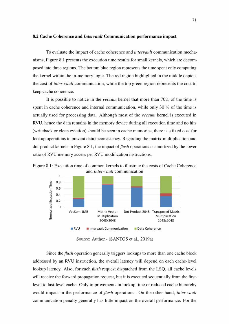
71
8.2 Cache Coherence and Intervault Communication performance impact
To evaluate the impact of cache coherence and intervault communication mecha-
nisms, Figure 8.1 presents the execution time results for small kernels, which are decom-
posed into three regions. The bottom blue region represents the time spent only computing
the kernel within the in-memory logic. The red region highlighted in the middle depicts
the cost of inter-vault communication, while the top green region represents the cost to
keep cache coherence.
It is possible to notice in the vecsum kernel that more than 70% of the time is
spent in cache coherence and internal communication, while only 30 % of the time is
actually used for processing data. Although most of the vecsum kernel is executed in
RVU, hence the data remains in the memory device during all execution time and no hits
(writeback or clean eviction) should be seen in cache memories, there is a fixed cost for
lookup operations to prevent data inconsistency. Regarding the matrix-multiplication and
dot-product kernels in Figure 8.1, the impact of flush operations is amortized by the lower
ratio of RVU memory access per RVU modification instructions.
Figure 8.1: Execution time of common kernels to illustrate the costs of Cache Coherenceand Inter-vault communication
0
0.2
0.4
0.6
0.8
1
VecSum 1MB Matrix VectorMultiplication
2048x2048
Dot Product 2048 Transposed MatrixMultiplication
2048x2048No
rmal
ized
Exe
cuti
on
Tim
e
RVU Intervault Communication Data Coherence
Source: Author - (SANTOS et al., 2019a)
Since the flush operation generally triggers lookups to more than one cache block
addressed by an RVU instruction, the overall latency will depend on each cache-level
lookup latency. Also, for each flush request dispatched from the LSQ, all cache levels
will receive the forward propagation request, but it is executed sequentially from the first-
level to last-level cache. Only improvements in lookup time or reduced cache hierarchy
would impact in the performance of flush operations. On the other hand, inter-vault
communication penalty generally has little impact on the overall performance. For the

72
transposed matrix-multiplication kernel, it is possible to see the effect of a great number of
register-read and mem-read to different vaults inherent to the application loop.
Regarding flush operations and intervault communication as costs that could be
avoided, in Figure 8.2 it is shown the overall performance improvement of an ideal RVU
(no flush and no intervault communication), and the performance penalty employing
the work’s proposal in some benchmarks of Polybench Suite. In general, the present
mechanism can achieve speed-up improvements between 2.5× and 14.6×, while using
82% of the execution time for computation, and hence only 18% for cache coherence and
inter-vault communications. Therefore, our proposal provides a competitive advantage in
terms of speedup in comparison to other HMC-instruction-based RVU setups. For instance,
the proposal presented in (NAI et al., 2017) relies on uncacheable data region, hence no
hardware cost is introduced. However, it comes with a cost in how much performance
can be extracted when deciding if a code portion must be executed in the host core or in
RVU units. Besides, the speculative approach proposed in (BOROUMAND et al., 2016)
has only 5% of performance penalty compared to an ideal RVU, but the performance can
profoundly degrade if rollbacks are frequently made, which will depend on the application
behavior. Also, another similar work (AHN et al., 2015) advocates locality-aware PIM
execution to avoid flush operations and off-chip communication. However, they do not
consider that large vectors in RVU can amortize the cost of cache coherence mechanism
even if, eventually, the host CPU has to process scalar operands on the same data region.
Figure 8.2: Execution time of PolyBench normalized to AVX-512
0.00
0.10
0.20
0.30
0.40
Exec
uti
on
Tim
e -
No
rmal
ized
to
AV
X5
12
RVU Data Coherence and Communication Performance Penalty
Source: Author - (SANTOS et al., 2019a)

73
8.3 Vector Selector performance impact
As presented in Chapter 7.2, different vector operand sizes can be scheduled by
the compiler in order to improve SIMD operation. However, it is important to select the
largest possible vector size to exploit HMC’s internal parallelism efficiently.
Figure 8.3 illustrates the impact of the suitable vector size selection on RVU PIM
architecture for different kernels with different input sizes. In this evaluation, each kernel
application is compiled for different target sizes, as described in Table 8.1, ranging from
128 Bytes to the maximum size given by the architecture specification (8192 Bytes) or the
maximum size possible for each input size. For this, at compile time, the flag -vector-force-
width can be used to manually inform the compiler which vector size to use. Although the
input size contributes to the choice of the operand size, the results show that each algorithm
has different requirements that dictate the optimal operand size. In this way, the results
presented here clearly highlight the significance of PRIMO in deciding the most favorable
vector size.
Figure 8.3a presents results for a regular-pattern Vector Sum kernel running different
workloads. It is possible to notice that for each workload the largest possible vector operand
Figure 8.3: Vector Size analysis on different kernels for floating-point computation.All results normalized to RVU128B.
1.1
0
02468
10121416
256B 1kB 2kB 4kB 8kB 128kB
Vector SizeSpee
du
p o
ver
RV
U1
28
B
R256 R512 R1024 R2048 R4096
(a) Vector Sum
0
1
2
3
512Bx512B 1kBx1kB 4kBx4kB 8kBx8kB
Matrix SizeSpee
du
p o
ver
RV
U1
28
B
R256 R512 R1024 R2048 R4096
(b) Stencil 5p
0
5
10
15
2kB 8kB 16kB 128kB 4MB
Vector SizeSpee
du
p o
ver
RV
U1
28
B
R256 R512 R1024 R2048 R4096
(c) Dot Product
1.1
0
0
2
4
6
8
10
12
14
512B 4kB 8kB 16kB
Matrix Size
Spee
du
p o
ver
RV
U1
28
B
R256 R512 R1024 R2048 R4096
(d) Matrix Vector Multiplication
Source: Author - (AHMED et al., 2019)

74
size can be set. One can observe that the compiler favors instructions with smaller vector
operand size to match the input size of small workloads. This behavior is illustrated in
the workloads ranging from 256B to 8kB, where the largest instruction size for each input
size gives better performance in comparison to all remaining sizes. In this way, PRIMO’s
decision of always choosing the largest vector width is found to be an optimal choice for
vecsum-like application in terms of performance.
Although the allocation of operands bigger than the input size is possible (e.g.,
operating through 256 Bytes of data and an RVU of 1024 Bytes), this behavior will reduce
the efficiency of the system, as it requires the use of mask to select the proper elements
of the vector (similar to AVX-512), or data could be incorrectly modified. Because of
this, PRIMO tries to avoid unnecessary operations, by matching the operand size and the
workload. In this case, PRIMO tries to allocate the biggest operand size, always seeking
the greatest possible vectorization, as presented in the Chapter 7.2.
The impact of vector size technique on the 5p Stencil kernel is shown in the Fig-
ure 8.3b. When the workload size is 512Bx512B the largest possible operand R512 shows
greater performance in comparison to R256. Similarly, when the input size is increased
to 1kBx1kB, the largest operand R1024 shows maximum performance in comparison to
R256 and R512. However, for the data size of 4kBx4kB, R1024 gives a better outcome
in comparison to R2048. Finally, with 8kBx8kB size, R2048 and R1024 are better than
R4096. Hence, for stencil application represented in the Figure 8.3b, it can be observed
that the behavior of operand size is not monotonic in the manner that performance is
not always increased by increasing the vector sizes. In this way, for stencil application
PRIMO’s vector size selection appears to be optimal for certain workloads, but for others,
some smaller size operand performs even better.
The stencil kernel presents a memory-unaligned access on part of the code, which
can be observed mainly on bigger workload sizes. For a matrix of 512Bx512B and
1024Bx1024B speedup increases accordingly with operand size. However, for 4096Bx4096B
and 8192Bx8192B, due to the unaligned access, it is not possible to allocate the operand
and workload of the same size.
Figure 8.3c presents the results for the Dot Product kernel. When the data size
is 2kB, the largest possible width of R512 appears to be slower in comparison to R256.
This exemplifies some of the drawbacks of vector size technique for small workloads. In
this case, the kernel has two different parts, and just one of them can be reused when
the workload is increased. Also, PRIMO chooses a more efficient sequence of R256B

75
instructions that avoids intervault requests for the kernel part which is not reused. In short,
the code targeting R512B instructions can only be amortized in larger workloads.
Similarly, with data size of 16kB and 128kB, R2048 instructions shows better
performance than the largest size of R4096, as shown in the Figure 8.3c. Whereas, for the
data size of 8kB and 4MB, R4096 gives slightly better performance than the remaining
operand sizes. For this kernel, the largest vector size is not the optimal size for all cases. It
can be explained by the increasing amount of intervault requests and the higher latencies
that occur between different level of the network connecting PIM units when computing
R4096 instructions. In this case, the instruction mapping can take advantage of parallel
access by scheduling instructions of 2048 Bytes that can access more vaults in parallel with
lower interconnection latency, overcoming the performance achieved by the RVU 4096B.
The speedups obtained for matrix-vector multiplication kernel are shown in the
Figure 8.3d. For small workloads (i.e., 512B) R256 operands show little performance
improvement in comparison to the baseline. However, as the workload size is increased, a
larger operand size can be used, while providing a growing performance improvement. In
the case of matrix-vector multiplication, the largest vector width appears to be the optimal
operand size as for all cases it gives maximum performance.
It can be observed through the results presented in Figure 8.3 that the selection of
optimal vector size is critical as it can lead to great performance improvement by exploiting
the maximum capability of SIMD instructions in a PIM hardware. In this way, for certain
applications PRIMO’s vector size selector can fetch the maximum performance from the
available PIM machine by automatically selecting the largest vector sizes. Hence, it saves
the programmer from the burden of selecting optimal size manually.
However, the largest vector width (e.g., R4096B) is not optimal for all applications.
In this way, the situation is not deterministic because the largest size can bring the best
results in certain cases, while in others it might lead to reduced performance. The possible
reason for this behavior is, when PRIMO tries to use vector operators in a loop, the
data must be gathered from different memory regions in small parts, harming the overall
performance. Also, in certain situations, larger sizes could lead to hardware overhead,
underutilization, and saturation of performance. In this way, the largest sizes are not always
optimal for all applications. It means that operand size selection is sensitive to application
characteristics as well.

76
8.4 VPU Selector performance impact
Another important issue on multi-instances PIM style is the efficient utilization of
distributed FUs. The use of one or a few parallel RVUs reduces the communication between
register banks located in different vaults. However, it increases the cross-references to
distinct vaults for memory requests, which reduces the efficiency of the setup. By setting
affinity to PIM instructions, which means to match the RVU instance with the vault that
data resides, it is possible to exploit the inherent parallelism and high-speed transferring
available within each vault while reducing the communication between different vaults.
This section evaluates the performance obtained by implementing the VPU se-
lection algorithm presented in Chapter 7.3. The operand sizes were varied from R128
to the maximum size, e.g., R4096, to better illustrate the performance achieved when
compiled with VPU enabled (VPU-ON) and the technique disabled (VPU-OFF). The
improvement provided by the PRIMO’s VPU Selector algorithm is shown in the Figure 8.4,
which focuses on a uniform distribution of instructions along PIM instances to increase
performance. The results demonstrate that the VPU Selector technique can improve in up
to 4.1× the utilization of PIM instances.
For the vecsum kernel, with the size of 1kB, both VPU-ON and VPU-OFF show
little improvement over the baseline, and the speedup of VPU-ON over VPU-OFF is also
small. This little improvement is because the small workload is not enough to amortize
the offloading cost and show the benefit of large vector sizes and VPU selection. When
the workload is increased to 2kB, R1024 with VPU-ON shows the maximum speedup
over the baseline. For this workload, the operand sizes of R512 and R1024 show a minor
difference between VPU-ON and VPU-OFF. The reason behind this is that, larger vector
sizes can already exploit multiple vaults, like R512 uses two vaults instead of only one
synchronously. Similarly, R1024 uses four vaults. In this way, even without VPU-ON, the
performance is not as bad as in the case of R256.
Moreover, the VPU selection shows a decreasing effect as the speedup gets reduced
linearly by increasing operand size. The workload of 4kB and the larger ones show a
different picture. The speedup of VPU-ON over VPU-OFF is maximum with R512, i.e.,
1.9×, instead of R256. Similarly, for the workloads of 8kB and 128kB, R512 achieves
a maximum speedup concerning VPU-ON over VPU-OFF, 3.1× and 2.7×, respectively.
It can be observed that the speedups of VPU selection are not only achieved with R256
and R512 but with other vector sizes as well including R128, R1024, R2048, and R4096.

77
Figure 8.4: RVU Selector Analysis on different kernels for floating-point computations.All results normalized to RVU128B.
Bas
elin
e 1
kB
Bas
elin
e 2
kB
Bas
elin
e 4
kB
Bas
elin
e 8
kB
Bas
elin
e 1
28
kB
0
2
4
6
8
10
R2
56
R5
12
R1
28
R2
56
R5
12
R1
02
4
R1
28
R2
56
R5
12
R1
02
4
R2
04
8
R1
28
R2
56
R5
12
R1
02
4
R2
04
8
R2
56
R5
12
R1
02
4
R2
04
8
R4
09
6
1kB 2kB 4kB 8kB 128kB
Spee
du
p o
ver
Bas
elin
es
VPU-OFF VPU-ON
(a) Vector Sum
Bas
elin
e 4
kB
Bas
elin
e 8
kB
0
1
2
3
4
5
R512 R1024 R128 R256 R512 R1024 R2048 R4096
4kB 8kB
Spee
du
p o
ver
Bas
elin
e
VPU-OFF VPU-ON
(b) Stencil 5p
Bas
elin
e 8
kB
Bas
elin
e 1
6kB
Bas
elin
e 1
28
kB
Bas
elin
e 4
MB
0
2
4
6
8
10
12
R1
28
R1
02
4
R1
28
R2
56
R5
12
R1
02
4
R2
56
R5
12
R1
02
4
R2
04
8
R2
56
R5
12
R1
02
4
R2
04
8
8kB 16kB 128kB 4MB
Spee
du
p o
ver
Bas
elin
e
VPU-OFF VPU-ON
(c) Dot Product
Bas
elin
e 4
kB
Bas
elin
e 8
kB
Bas
elin
e 1
6kB
012345678
R128 R256 R512 R1024 R256 R512 R1024 R256 R512 R1024 R2048
4kB 8kB 16kB
Spee
du
p o
ver
Bas
elin
e
VPU-OFF VPU-ON
(d) Matrix Vector Multiplication
Source: Author - (AHMED et al., 2019)
However, here we have only discussed the maximum speedups achieved. Furthermore, the
impact of VPU selection gets decreased, and the overall speedup relative to the baseline is
increased with larger operand sizes.
Figure 8.4b shows the impact of VPU selection on the 5-point stencil application.
It can be observed that VPU selection has a low impact on small workloads (4kB), but,
when the size is increased to 8kB, a more significant impact can be observed. Although
R1024 gives the maximum performance in comparison to the baseline, the maximum VPU
selection speedup (i.e., 2.5x) is attained with R256. In this way, the VPU selection appears
to be more beneficial in case of R256. Also, the impact of VPU selection starts decreasing,
and the overall speedup relative to the base is increased with larger operand sizes.
The impact of VPU selection on the dot product kernel can be observed in Figure
8.4c. For small workloads (8kB), R1024 presents the greatest gains (i.e., 1.3×) for VPU-
ON over VPU-OFF. When the workload is increased to 16kB, R256 attains the maximum
VPU selection speedup i.e., 3.15x. The reason for this much speedup is the use of multiple
vaults with VPU-ON in comparison to a single vault with VPU-OFF. Furthermore, with
more increase in vector operand sizes, the VPU-ON speedup gets lowered because VPU-
OFF is also capable of exploiting multiple vaults. The input sizes of 128kB and 4MB show
similar behavior. The VPU speedup is maximum with R256. VPU-ON/VPU-OFF ratio
gets reduced, but the overall speedup over the baseline is increased with larger operand

78
sizes.
Finally, the Figure 8.4d shows VPU selection impact for matrix-vector multipli-
cation kernel. For all workloads, R256 shows maximum VPU selection speedup. Also,
for all cases, the VPU selection speedup tends to saturate by increasing the operand size.
However, the VPU selection technique can increase the performance for the remaining
operand sizes as well. Also, by increasing operand sizes, the VPU-ON/VPU-OFF ratio
gets lowered, but the overall speedup is increased with respect to the baseline.
Overall, it can be observed that the ratio of VPU-ON and VPU-OFF is maximum
for smaller vector size like R256 and R512. This is because by default it makes use of a
few or a single vault and VPU selection technique enables it to use more than one vault at
the same time. Further, it can be seen how this VPU-ON/VPU-OFF ratio gets reduced by
increasing vector sizes. Still, VPU selection improves performance for large size operands
but the impact is lesser as compared to R256. By increasing the operand sizes, the overall
performance gets improved with respect to the base machine. Therefore, it can be said that
the maximum speedup in comparison to the baseline machine, is achieved by using the
largest possible vector size and VPU selection technique.
8.5 Performance Breakthrough
To show the applicability of RVU and PRIMO, the PolyBench Benchmark Suite
(POUCHET, 2012) was experimented, and the generated binaries were executed in the
custom GEM5 simulator. Figure 8.5 compares the RVU PIM and the baseline AVX-512
processor. Also, Figure 8.5 directly compares the ability of the compiler in extracting more
performance from RVU architecture running PolyBench kernels. Without PRIMO’s VPU
Selector technique, RVU achieves an average speedup of 8.1×, while the average speedup
jumps to 15.9× by enabling VPU Selector mechanism. On average, VPU selector improves
the execution time by 2×, which demonstrate the importance of efficiently generate and
offload code to use multiple PIM instances.
As shown in Figures 8.5a, 8.5b and 8.5c, the performance is improved as the
workload is increased, achieving a maximum speedup of 26× with R1024 VPU-ON.
Whereas, R512 (RVU operating through 512 Bytes) achieves the highest gain when
comparing VPU-ON over VPU-OFF, i.e. 2.72×. Regarding the bicg kernel depicted in
the Figures 8.5d, 8.5e and 8.5f, the highest speedup over the AVX baseline is achieved
by using R512 operands and VPU-ON for large inputs (2048x2048). The bicg kernel

79
for medium input size (1024x1024) shown in Figure 8.5e is less impacted by PRIMO’s
optimization than atax (Figure 8.5b), which has a speedup of 13.1× for the same input size.
This is due to application characteristics, as atax contains more vectorization opportunities
than bicg.
Similarly, the doitgen kernel shown in Figures 8.5g and 8.5h presents maximum
speedup of 24× by using R1024 with VPU-ON in the workload of 256x256x256 elements.
It is interesting to notice for doitgen kernel, despite of using a three-dimensional matrix
workload, the innermost loop can be totally unrolled hence taking advantage of the biggest
vector operands provided by RVU architecture. Therefore, in this case, each innermost
loop operation fits into a single RVU vector operand, which allow the elimination of most
internal iterations. The workload 128x128x128 uses the RVU instruction R512, and it
shows the speedup of 11.5×. In case of VPU-ON vs VPU-OFF speedup, both R512 and
R1024 give improvement of 4.0×.
Figures 8.5i and 8.5j shows kernel deriche with R2048 and R4096 having different
input sizes. Although the evident ability for vectorization, the compiler is not able to
widely improve performance of the Deriche application by scheduling the RVU instances
in case of largest vectors. This is because the larger the selected vector (or group of RVUs),
the less room for acting the compiler has. This makes it even more difficult to scale to other
vector units, which would also use a large vector. Therefore, Figure 8.5i presents speedup
of 33× for VPU-ON, while VPU-OFF achieves 21×, both cases operating over 2048 Bytes.
Figure 8.5j shows the adoption of R4096, and in this case the speedup achieved is 32×
and 36× for VPU-OFF and VPU-ON respectively.
In Figures 8.5k and 8.5l, gemver is tested with R1024 and R2048. In this case,
the maximum speedup over the baseline is achieved by R2048 VPU-ON, although the
improvement of VPU selection is maximum for R1024. Regarding mvt kernel represented
by Figures 8.5m and 8.5n, the overall speedup with respect to the baseline is maximum
when R2048 is used with VPU selection. Similarly, VPU-ON vs VPU-OFF is maximum
for smaller operands i.e. R128. Finally, Figures 8.5o and 8.5p shows results for covariance
kernel. It can be seen the speedup relative to the baseline is maximum with R1024 and
VPU-ON. The performance of VPU-ON vs VPU-OFF is maximum with R256.
Through Figure 8.5, the importance of both large vector size and VPU selection can
be observed. It can be seen how large vector sizes improve performance with respect to the
baseline, although the largest value cannot be considered optimal size for all applications,
as discussed in the Chapter 7. In addition to the vector size technique, the performance can

80
be further improved by using the VPU selection technique, which is found to be reasonable
for all application scenarios and operand sizes. However, the effect of the proper RVU
selection through the VPU Selector module gets more prominent for smaller operand
sizes where the performance by VPU-ON is largely improved in comparison to VPU-OFF.
Another interesting point to observe is that applications from the same class of PolyBench
executed with the same input size and operand size have different behaviors in terms of
performance and optimization. Thus, the use of the proposed technique depends on the
Figure 8.5: Speedup over the AVX-512 baseline for different kernels of the PolyBenchsuite
1
2
3
4
5
ATAX 512x512
R256 VPU-OFF R256 VPU-ON
(a)
1
3
5
7
9
11
13
15
ATAX 1024x1024
R512 VPU-OFF R512 VPU-ON
(b)
1
6
11
16
21
26
ATAX 2048x2048
R1024 VPU-OFF R1024 VPU-ON
(c)
1
2
3
4
BICG 512x512
R128 VPU-OFF R128 VPU-ON
(d)
1
3
5
7
9
11
BICG 1024x1024
R256 VPU-OFF R256 VPU-ON
(e)
1
5
9
13
17
21
25
BICG 2048x2048
R512 VPU-OFF R512 VPU-ON
(f)
1
3
5
7
9
11
DOITGEN 128x128x128
R512 VPU-OFF R512 VPU-ON
(g)
1
5
9
13
17
21
25
DOITGEN 256x256x256
R1024 VPU-OFF R1024 VPU-ON
(h)
1
5
9
13
17
21
25
29
33
DERICHE 512x512
R2048 VPU-OFF R2048 VPU-ON
(i)
1
6
11
16
21
26
31
36
DERICHE 1024x1024
R4096 VPU-OFF R4096 VPU-ON
(j)
1
4
7
10
GEMVER 1024x1024
R1024 VPU-OFF R1024 VPU-ON
(k)
1
4
7
10
13
16
19
22
GEMVER 2048x2048
R2048 VPU-OFF R2048 VPU-ON
(l)
1.0
1.5
2.0
2.5
MVT 512x512
R128 VPU-OFF R128 VPU-ON
(m)
1
6
11
16
MVT 2048x2048
R2048 VPU-OFF R2048 VPU-ON
(n)
1.0
1.5
2.0
2.5
COVARIANCE 256x256
R256 VPU-OFF R256 VPU-ON
(o)
1
2
3
4
COVARIANCE 512x512
R1024 VPU-OFF R1024 VPU-ON
(p)
Source: Author

81
application characteristics to obtain the optimal point. Also, certain applications possess
more vectorization opportunities as compared to others, which directly translates to the
better use of the techniques.

82
8.6 Energy Breakthrough
Figure 8.6 presents the energy consumption for PolyBench applications normalized
to AVX-512. Similarly to Figure 8.5, it shows results for both cases: VPU Selector enabled
and disabled. By analyzing this results, it is possible to notice the efficiency of RVU design
and PRIMO compiler.
The impact of avoiding data movement through complex cache memory hierarchies,
unnecessary register spills and cache memory evictions is noticeable. For ATAX application,
a reduction of 92% on energy consumption can be observed for the largest workload
(2048x2048) and use of R2048. Similar results can be noticed for BICG, DOITGEN, and
DERICHE. Also, MVT and GEMVER achieve 92% of energy reduction when operating
over 2048x2048 elements. Other applications and workloads also present improvement,
ranging from 55% to 80% of energy reduction. The worst case scenario occurs on
COVARIANCE, which for 256x256 achieves a reduction of only 8% on energy consumption.
The two main reasons are the accumulations over scalars, which by default trigger memory
accesses that can use the cache memories, and also benefit from host’s higher frequencies
(4GHz vs 1GHz - Table 8.1). Therefore, a possible solution to achieve better results is to
implement a mem2reg optimization on compiler in order to further reduce the offloading
of memory instructions.
Considering the performance improvements presented in Figure 8.5, it is expected
that the energy consumption follows the same path. However, as it can be observed, the
impact of additional RVU units cannot improve energy efficiency in the same way as
performance.
In case of ATAX experiment (Figures 8.6a, 8.6b, and 8.6c), additional RVU instances
improve performance and energy efficiency. However, the energy efficiency for the
workload of 2048x2048 is slightly better when VPU-ON is adopted, while performance
improvement is considerable (Figure 8.5c). This shows that the use of all RVU instances
can improve performance, but not necessarily achieves the best energy efficiency, since
extra units on imply in extra power dissipation in a larger proportion. This behavior also
happens in different applications on PolyBench Suite, and in some cases, the use of all
PIM units can even reduce energy efficiency when compared against reduced number of
RVUs. Figures 8.6i, 8.5j, 8.5k, 8.5l, 8.5m, 8.5n, and 8.6p illustrates this case.

83
Figure 8.6: Energy over the AVX-512 baseline for different kernels of the PolyBench suite
0.00
0.10
0.20
0.30
0.40
ATAX 512x512
R256 VPU-OFF R256 VPU-ON
(a)
0.00
0.05
0.10
0.15
0.20
0.25
ATAX 1024x1024
R512 VPU-OFF R512 VPU-ON
(b)
0.00
0.02
0.04
0.06
0.08
0.10
ATAX 2048x2048
R1024 VPU-OFF R1024 VPU-ON
(c)
0.00
0.25
0.50
0.75
BICG 512x512
R128 SEL-OFF R128 VPU-ON
(d)
0.00
0.05
0.10
0.15
0.20
0.25
BICG 1024x1024
R256 VPU-OFF R256 VPU-ON
(e)
0.00
0.02
0.04
0.06
0.08
0.10
0.12
0.14
BICG 2048x2048
R512 VPU-OFF R512 VPU-ON
(f)
0.00
0.08
0.16
0.24
0.32
0.40
DOITGEN 128x128x128
R512 VPU-OFF R512 VPU-ON
(g)
0.00
0.03
0.06
0.09
0.12
0.15
0.18
DOITGEN 256x256x256
R1024 VPU-OFF R1024 VPU-ON
(h)
0.00
0.02
0.04
0.06
0.08
0.10
DERICHE 512x512
R2048 VPU-OFF R2048 VPU-ON
(i)
0.00
0.01
0.02
0.03
0.04
0.05
0.06
0.07
DERICHE 1024x1024
R4096 VPU-OFF R4096 VPU-ON
(j)
0.00
0.05
0.10
0.15
0.20
GEMVER 1024x1024
R1024 VPU-OFF R1024 VPU-ON
(k)
0.00
0.02
0.04
0.06
0.08
0.10
0.12
0.14
GEMVER 2048x2048
R2048 VPU-OFF R2048 VPU-ON
(l)
0.00
0.20
0.40
0.60
0.80
1.00
MVT 512x512
R128 SEL-OFF R128 VPU-ON
(m)
0.00
0.02
0.04
0.06
0.08
0.10
0.12
0.14
0.16
MVT 2048x2048
R2048 VPU-OFF R2048 VPU-ON
(n)
0.90
0.92
0.94
0.96
0.98
1.00
COVARIANCE 256x256
R256 VPU-OFF R256 VPU-ON
(o)
0.00
0.10
0.20
0.30
0.40
0.50
0.60
0.70
COVARIANCE 512x512
R1024 VPU-OFF R1024 VPU-ON
(p)
Source: Author
84
9 CONCLUSIONS AND FUTURE WORK
This chapter summarizes the thesis, presents an overview of our findings and con-
tributions, some recommendations for improvement and future work, and the conclusion.
9.1 Summary
In Chapter 1 we set out three research topics for this thesis. The first one was
What are the most critical drawbacks of today’s computer architectures?. After substantial
research investigation and analysis of the last 10 years of modern processor architectures,
several traditional architecture limitations on different areas are presented in Chapter 2.
Chapter 2 concludes that performance and energy efficiency in these designs are directly
dependent on technological node, which is drastically constrained due to materials adopted
and physical specifications. Therefore, this study shows that a new approach is required to
improve overall efficiency of those systems. Here, as the main objective of this thesis, the
adoption of Processing-in-Memory (PIM) is a possible solution, as motivated by Chapter 4
and Chapter 8.
The second topic states: What are the most critical challenges for adopting PIM
in a general-purpose scenario?. Chapter 4 lists the most prominent PIM designs that
aim general-purpose applications. Although they can be compared to typical General
Purpose Processors (GPPs), either their performance, energy efficiency or area are present
as real contribution, and rarely all requirements are performed at same time. Moreover,
other important issues are frequently left aside, like cache coherence, virtual memory
management, and programmability. Therefore, for integrating PIM to the general-purpose
environment, all requisites must be properly filled. This way, we find that a new PIM design
is required to achieve the proposed objective, which must be disruptive in its essence, and
must present a complete solution as above mentioned.
The last and most important question is: Which PIM design can improve overall
performance and efficiency? This question can be answered by analyzing the PIM ar-
chitectures present in literature, which mainly implement full cores. Today’s processing
cores present a bunch of limitations (Chapter 2), and even more drawbacks exist when
full cores are implemented (i.e. cache hierarchy). Furthermore, those PIM implementa-
tions (Chapter 4) cannot achieve the expected high performance and energy efficiency
comparing against GPP. Also, the embedded nature of PIM devices demands area and

85
power efficiency within critical constraints. Considering these facts, Chapter 5 presents an
innovative PIM design (though simple) implementing only Functional Units (FUs). The
presented design, named Reconfigurable Vector Unit (RVU), meets the power and area
constraints. Additionally, the challenges discussed in Chapter 4 are solved, which allow the
insertion of the implemented RVU in the general-purpose environment improving overall
performance, as presented in Chapter 6. Moreover, in order to allow fully exploitation
of the RVU design, Chapter 7 shows the Processing-In-Memory cOmpiler (PRIMO), a
compiler to automatically generate code for RVU without additional user intervention,
programming efforts, or special libraries of any kind.
The evaluations for the different modules of PRIMO are presented in Chapter 8.
Moreover, this chapter presents results for several applications and benchmarks being
executed on RVU. Also, comparisons against GPPs are shown in this chapter.
9.2 Contributions
In retrospect, important contributions have been made by answering the questions
raised at the beginning of this thesis.
Highlighting the limitations of today’s architectures can be selected as a foremost
motivation to point out the necessity for new approaches. This step shows that, although
new technologies are expected for the future as new researches are a constant, the current
designs must be revised and updated to allow full exploitation of the available resources.
Secondly, this thesis investigate the most prominent PIM devices in literature. Through
this investigation and profound analysis, this thesis concludes that typical processing cores
are not suitable for PIM implementation. Therefore, a new approach should be taken.
From these efforts, the RVU PIM design is created ensuring the constraints of power and
area, at the same time being capable of exploiting the available resources. From these
efforts, the RVU PIM design is created. RVU can extract maximum bandwidth from
3D-stacked memories, and theoretically, it is able to achieve 2 TFLOPS of performance
(Single Precision Floaing-Point Operations per Second (SP-FLOPS)), while present a
power efficiency of 232GLOPS/Watt.
The integration with general-purpose environment is result of a custom data-path,
which ensures automatic instruction offloading and data coherence. In practice, the
presented architecture achieves 1.773 TFLOPS in a controlled experiment, resulting in
205GFLOPS/Watt. These results reflect in high performance when compared against

86
traditional GPP architecture, showing a speedup up to 30×. Furthermore, the presented
design drastically reduces energy consumption. By processing directly in memory, it
is able to avoid complex memory hierarchies, reducing data movement and therefore
achieving up to 92% of energy reduction. The experimentation of our design was supported
by a fully functional simulator based on GEM5. To efficiently exploit the RVU, is is
presented PRIMO. This compiler automatically decides where a portion of code should
run, host or PIM. Hence PRIMO is able to offload suitable PIM codes requiring no user
intervention, no special libraries or pragmas, and no programmer’s special skills. Also,
it is totally compatible with legacy codes, only demanding new compilation. On our
simulations, several PolyBench Benchmark Suite kernels were used to widely evaluate the
RVU architecture and PRIMO.
9.3 Conclusions
This work presents an approach to increase the overall efficiency of general-purpose
systems by adopting a PIM design. In this thesis we have presented the RVU, although
disruptive in the form, it uses same traditional units present in typical GPPs. Therefore, a
non-orthodox PIM that coupled with the PRIMO compiler, another contribution of this
work, significantly improves performance and energy efficiency of general-purpose sys-
tems. Several experiments and applications were performed, and the design implemented
increases performance by 15× in average, while reducing the energy consumption by 80%.
In the worst case, the proposed design achieves speedup of 2×, and energy reduction of
less than 2% running Correlation kernel. While in the best case, it achieves speedup of
36× with energy reduction of 92% for Deriche kernel.
9.4 Future work and Recommendations for Improvement
Chapter 8 showed that the architecture that was developed can be fully integrated
in a general-purpose environment with significant improvement in performance and energy.
Also, the same chapter shows that it is possible to totally avoid to burden programmers
with complex decisions, preventing the use of libraries and special pragmas by adopting
a compiler able to exploit the proposed architecture. Although these are significant
contributions, there is still room for further improvements.

87
The first one is related to host processor modifications. In our implementation,
the host’s decode stage must be updated to support new PIM Instruction Set Architecture
(ISA). Another host modification implemented in our approach is the additional hardware
responsible for cache coherence. Although area and power can be neglected in these
cases due to the minor additions, the host processor design must support it, which requires
manufacturer acceptance and project updates. In either case, the proposal is to take a
software approach. One way to avoid decoding stage updating is by embedding PIM
instructions into host native instructions in some way. In similar way, it is possible to
avoid the necessity of cache coherence hardware mechanism by adopting some approach
in software. However, both cases obviously increase the compiler complexity.
Another important improvement is enabling massive scalar operations in the RVU.
This will require more intelligence in the compilation process, making it recognize patterns
that have reduced temporal locality, or streaming behavior even when it occurs in scalar
format, for example. Although this thesis presents a compiler able to automatically generate
code for PIM, which reduces the programming efforts, it is not optimal. The selection of
vector sizes can also be improved, allowing a better distribution of tasks within a basic
block. Also, the selection of PIM units must be improved to further reduce intervault
communication.
As applications continue to rely on huge amounts of data, the principles proposed
in this thesis are expected to reach main stream products, and hence further research will
be needed in the near future.

88
REFERENCES
AHMED, H. et al. A compiler for automatic selection of suitable processing-in-memoryinstructions. In: Design, Automation & Test in Europe Conference & Exhibition(DATE). [S.l.: s.n.], 2019.
AHN, J. et al. A scalable processing-in-memory accelerator for parallel graph processing.In: IEEE. Int. Symp. on Computer Architecture (ISCA). [S.l.], 2015.
AHN, J. et al. A scalable processing-in-memory accelerator for parallel graph processing.ACM SIGARCH Computer Architecture News, ACM, v. 43, n. 3, p. 105–117, 2016.
AHN, J. et al. Pim-enabled instructions: a low-overhead, locality-aware processing-in-memory architecture. In: IEEE. Int. Symp. on Computer Architecture (ISCA). [S.l.],2015. p. 336–348.
AKIN, B.; FRANCHETTI, F.; HOE, J. C. Data reorganization in memory using 3d-stackeddram. In: ACM. ACM SIGARCH Computer Architecture News. [S.l.], 2015. v. 43,n. 3, p. 131–143.
ALVES, M. A. Z. et al. Opportunities and challenges of performing vector operationsinside the dram. In: Int. Symp. on Memory Systems (MemSys). [S.l.: s.n.], 2015.
ALVES, M. A. Z. et al. Saving memory movements through vector processing in the dram.In: Proceedings of the 2015 International Conference on Compilers, Architectureand Synthesis for Embedded Systems. Piscataway, NJ, USA: IEEE Press, 2015.(CASES ’15), p. 117–126. ISBN 978-1-4673-8320-2.
ARM. ARM. big.LITTLE Technology. [S.l.], 2011. Available from Internet:<https://developer.arm. com/technologies/big-little>.
ARM. Arm A15. 2012. Disponível em: <http://infocenter.arm.com/help/topic/com.arm.doc.ddi0438g/DDI0438G_cortex_a15_r3p2_trm.pdf>.
ARM. Arm A35. 2016. Disponível em: <https://static.docs.arm.com/100236/0001/cortex_a35_trm_100236_0001_02_en.pdf>.
ARM. Arm A5. 2016. Disponível em: <http://infocenter.arm.com/help/topic/com.arm.doc.ddi0433c/DDI0433C_cortex_a5_trm.pdf>.
ARM. Arm A57. 2016. Disponível em: <http://infocenter.arm.com/help/index.jsp?topic=/com.arm.doc.subset.cortexa.a57/index.html>.
ARM. Arm Neon. 2019. Disponível em: <https://developer.arm.com/architectures/instruction-sets/simd-isas/neon>.
AZARKHISH, E. et al. Design and evaluation of a processing-in-memory architecturefor the smart memory cube. In: SPRINGER. Int. Conf. on Architecture of ComputingSystems (ARCS). [S.l.], 2016.
BOROUMAND, A. et al. LazyPIM: An Efficient Cache Coherence Mechanism forProcessing-in-Memory. IEEE Computer Architecture Letters, 2016.

89
BOWMAN, N. et al. Evaluation of existing architectures in iram systems. In: Workshopon Mixing Logic and DRAM. [S.l.: s.n.], 1997.
BRUINTJES, T. M. et al. Sabrewing: A lightweight architecture for combined floating-point and integer arithmetic. ACM Trans. Architecture and Code Optimization, ACM,v. 8, n. 4, jan. 2012.
CARDOSO, J. P. de L. PIM-gem5: a system simulator for Processing-in-Memorydesign space exploration. Dissertação (Mestrado) — Federal University of Rio Grandedo Sul - PPGC, 2 2019.
CHEN, K. et al. Cacti-3dd: Architecture-level modeling for 3d die-stacked dram mainmemory. In: Design, Automation & Test in Europe Conference & Exhibition (DATE).[S.l.: s.n.], 2012.
DENNARD, R. H. et al. Design of ion-implanted mosfet’s with very small physicaldimensions. IEEE Journal of Solid-State Circuits, v. 9, n. 5, 1974.
DRUMOND, M. et al. The mondrian data engine. In: ACM. Int. Symp. on ComputerArchitecture. [S.l.], 2017.
ECKERT, Y.; JAYASENA, N.; LOH, G. H. Thermal feasibility of die-stacked processingin memory. In: Proceedings of the 2nd Workshop Near-Data Processing. [S.l.: s.n.],2014. ISBN 978-3-319-30694-0.
ELLIOTT, D. et al. Computational ram: Implementing processors in memory. Design andTest of Computers, IEEE, 1999.
EXANODE. Report on the ExaNoDe architecture design guidelines. [S.l.], 2017.Http://exanode.eu/wp-content/uploads/2017/04/D2.2.pdf.
FARMAHINI-FARAHANI, A. et al. Drama: An architecture for accelerated processingnear memory. Computer Architecture Letters, 2014.
GAO, M.; KOZYRAKIS, C. HRL: efficient and flexible reconfigurable logic for near-dataprocessing. In: Int. Symp. High Performance Computer Architecture (HPCA). [S.l.:s.n.], 2016.
GAO, M. et al. Tetris: Scalable and efficient neural network acceleration with 3d memory.In: Int. Conf. on Architectural Support for Programming Languages and OperatingSystems. [S.l.: s.n.], 2017.
GOKHALE, M.; HOLMES, B.; IOBST, K. Processing in memory: The terasys massivelyparallel pim array. Computer, IEEE, v. 28, n. 4, p. 23–31, 1995.
HADIDI, R. et al. Cairo: A compiler-assisted technique for enabling instruction-leveloffloading of processing-in-memory. ACM Transactions on Architecture and CodeOptimization (TACO), v. 14, n. 4, p. 48, 2017.
HSIEH, K. et al. Transparent offloading and mapping (tom): Enabling programmer-transparent near-data processing in gpu systems. ACM SIGARCH ComputerArchitecture News, ACM, v. 44, n. 3, p. 204–216, 2016.

90
HSIEH, K. et al. Accelerating pointer chasing in 3D-stacked memory: Challenges,mechanisms, evaluation. In: Int. Conf. on Computer Design (ICCD). [S.l.: s.n.], 2016.
HUANG, L. et al. A new architecture for multiple-precision floating-point multiply-addfused unit design. In: Symposium on Computer Arithmetic (ARITH), 2007. [S.l.: s.n.],2007.
Hybrid Memory Cube Consortium. Hybrid Memory Cube Specification Rev. 2.0. 2013.Http://www.hybridmemorycube.org/.
INTEL. Intel Nehalem Processors Technical Manual. [S.l.], 2008. Disponívelem: <https://www.intel.com/content/dam/www/public/us/en/documents/manuals/64-ia-32-architectures-optimization-manual.pdf>.
INTEL. Intel Sandybridge Processors Technical Manual. [S.l.], 2013. Disponívelem: <https://www.intel.com/content/dam/www/public/us/en/documents/manuals/64-ia-32-architectures-optimization-manual.pdf>.
INTEL. Why has CPU frequency ceased to grow? 2014. Disponível em: <https://software.intel.com/en-us/blogs/2014/02/19/why-has-cpu-frequency-ceased-to-grow>.
INTEL. Intel AVX-512 Instructions. 2017. Disponível em: <https://software.intel.com/en-us/articles/intel-avx-512-instructions>.
INTEL. Architecture Extensions. 2018. Disponível em: <https://software.intel.com/en-us/isa-extensions>.
INTEL. Intel Core 9980XE eXtreme Edition. [S.l.], 2018. Disponívelem: <https://ark.intel.com/content/www/us/en/ark/products/189126/intel-core-i9-9980xe-extreme-edition-processor-24-75m-cache-up-to-4-50-ghz.html>.
INTEL. Intel Skylake-X Processors Technical Manual. [S.l.], 2018. Disponívelem: <https://www.intel.com/content/dam/www/public/us/en/documents/manuals/64-ia-32-architectures-optimization-manual.pdf>.
JEDDELOH, J.; KEETH, B. Hybrid memory cube new DRAM architecture increasesdensity and performance. In: Symp. on VLSI Technology. [S.l.: s.n.], 2012.
KANG, Y. et al. Flexram: toward an advanced intelligent memory system. In: Int. Conf.on Computer Design: VLSI in Computers and Processors. [S.l.: s.n.], 1999.
KERSEY, C. D.; KIM, H.; YALAMANCHILI, S. Lightweight simt core designs forintelligent 3d stacked dram. In: ACM. Int. Symp. on Memory Systems (MEMSYS).[S.l.], 2017.
KIM, D. et al. Neurocube: A programmable digital neuromorphic architecture withhigh-density 3d memory. In: IEEE. Int. Symp. on Computer Architecture (ISCA).[S.l.], 2016.
LATTNER, C.; ADVE, V. Llvm: A compilation framework for lifelong program analysis& transformation. In: IEEE COMPUTER SOCIETY. Int. Symp. on Code generationand optimization. [S.l.], 2004. p. 75.

91
Lee, C. et al. An overview of the development of a gpu with integrated hbm on siliconinterposer. In: 2016 IEEE 66th Electronic Components and Technology Conference(ECTC). [S.l.: s.n.], 2016. p. 1439–1444.
LEE, D. U. et al. 25.2 a 1.2 v 8gb 8-channel 128gb/s high-bandwidth memory (hbm)stacked dram with effective microbump i/o test methods using 29nm process and tsv. In:Int. Solid-State Circuits Conference Digest of Technical Papers (ISSCC). [S.l.: s.n.],2014.
LEE, J. H.; SIM, J.; KIM, H. Bssync: Processing near memory for machine learningworkloads with bounded staleness consistency models. In: IEEE. Int. Conf. on ParallelArchitecture and Compilation (PACT). [S.l.], 2015. p. 241–252.
LOH, G. H. et al. A processing in memory taxonomy and a case for studying fixed-functionpim. In: Workshop on Near-Data Processing. [S.l.: s.n.], 2013.
MANOLOPOULOS, K.; REISIS, D.; CHOULIARAS, V. An efficient multiple precisionfloating-point multiply-add fused unit. Journal of Microelectronic, v. 49, 2016.
MÄRTIN, C. Post-dennard scaling and the final years of moore’s law consequences for theevolution of multicore-architectures. Informatik und Interaktive Systeme, 2014.
MCGRAW-HILL. Von Neumann Bottleneck. [S.l.: s.n.], 2003. v. 6E.
MCINTOSH-SMITH, S. et al. A performance analysis of the first generationof hpc-optimized arm processors. Concurrency and Computation: Practiceand Experience, v. 0, n. 0, p. e5110, 2019. E5110 cpe.5110. Disponível em:<https://onlinelibrary.wiley.com/doi/abs/10.1002/cpe.5110>.
Moore, G. E. Progress in digital integrated electronics. IEEE Solid-State CircuitsSociety Newsletter, v. 11, n. 3, p. 36–37, Sep. 2006. ISSN 1098-4232.
MULTI-PROJETS, C. C. IC STMicroelectronics 28nm Advanced CMOS FDSOI 8ML CMOS28FDSOI. [S.l.], 2018. Https://mycmp.fr/datasheet/ic-28nm-cmos28fdsoi.
NAI, L. et al. Graphpim: Enabling instruction-level pim offloading in graph computingframeworks. In: IEEE. Int. Symp. on High Performance Computer Architecture(HPCA). [S.l.], 2017.
NAIR, R. et al. Active memory cube: A processing-in-memory architecture for exascalesystems. IBM Journal of Research and Development, IBM, v. 59, 2015.
NVIDIA. Nvidia Tesla V100. [S.l.], 2018. Disponível em: <https://www.nvidia.com/en-us/data-center/tesla-v100/>.
OLIVEIRA, G. F. et al. Nim: An hmc-based machine for neuron computation. In:SPRINGER. Int. Symp. on Applied Reconfigurable Computing (ARC). [S.l.], 2017.
OLMEN, J. V. et al. 3D stacked IC demonstration using a through Silicon Via Firstapproach. In: Int. Electron Devices Meeting. [S.l.: s.n.], 2008.
PATTERSON, D. et al. A case for intelligent ram. IEEE micro, IEEE, v. 17, 1997.

92
PAWLOWSKI, J. T. Hybrid memory cube (hmc). In: IEEE. Hot Chips 23 Symposium(HCS). [S.l.], 2011.
POUCHET, L.-N. Polybench: The polyhedral benchmark suite. URL:http://www.cs.ucla.edu/pouchet/software/polybench, 2012.
PUGSLEY, S. H. et al. Ndc: Analyzing the impact of 3d-stacked memory+ logic deviceson mapreduce workloads. In: Int. Symp. on Performance Analysis of Systems andSoftware (ISPASS). [S.l.: s.n.], 2014.
RAHMAN, R. Xeon phi cache and memory subsystem. In: . Intel® XeonPhi™ Coprocessor Architecture and Tools: The Guide for Application Developers.Berkeley, CA: Apress, 2013. p. 65–80. ISBN 978-1-4302-5927-5. Disponível em:<https://doi.org/10.1007/978-1-4302-5927-5_5>.
SANTOS, P. C.; ALVES, M. A.; CARRO, L. Hmc and ddr performance trade-offs.In: FIP TC10 Working Conference: International Embedded Systems Symposium(IESS). [S.l.: s.n.], 2015. (IESS ’15).
SANTOS, P. C. et al. Exploring cache size and core count tradeoffs in systems withreduced memory access latency. In: IEEE. Int. Conf. Parallel, Distributed, andNetwork-Based Processing (PDP). [S.l.], 2016.
SANTOS, P. C. et al. Solving datapath issues on near-data accelerators. In: IFIP WG10.2Working Conference: International Embedded Systems Symposium (IESS). [S.l.:s.n.], 2019. (IESS ’19).
SANTOS, P. C. et al. A technologically agnostic framework for cyber-physical and iotprocessing-in-memory-based systems simulation. Microprocessors and Microsystems,v. 69, p. 101 – 111, 2019. ISSN 0141-9331.
SANTOS, P. C. et al. Processing in 3d memories to speed up operations on complex datastructures. In: IEEE. Design, Automation & Test in Europe Conference & Exhibition(DATE). [S.l.], 2018.
SANTOS, P. C. et al. Operand size reconfiguration for big data processing in memory.In: IEEE. Design, Automation & Test in Europe Conference & Exhibition (DATE).[S.l.], 2017.
SAULSBURY, A.; PONG, F.; NOWATZYK, A. Missing the memory wall: The case forprocessor/memory integration. In: Int. Symp. on Computer Architecture (ISCA). [S.l.:s.n.], 1996.
SCHALLER, R. R. Moore’s law: past, present and future. IEEE Spectrum, v. 34, n. 6, p.52–59, Jun 1997.
SCRBAK, M. et al. Exploring the processing-in-memory design space. Journal ofSystems Architecture, Elsevier, v. 75, 2017.
SHAAFIEE, M.; LOGESWARAN, R.; SEDDON, A. Overcoming the limitations ofvon neumann architecture in big data systems. In: 2017 7th International Conferenceon Cloud Computing, Data Science Engineering - Confluence. [S.l.: s.n.], 2017. p.199–203.

93
SHAHAB, A. et al. Farewell my shared llc! a case for private die-stacked dramcaches for servers. 2018 51st Annual IEEE/ACM International Symposium onMicroarchitecture (MICRO), p. 559–572, 2018.
SHAHIDI, G. G. Chip power scaling in recent cmos technology nodes. IEEE Access, v. 7,p. 851–856, 2019. ISSN 2169-3536.
STILLMAKER, A.; BAAS, B. Scaling equations for the accurate prediction of cmosdevice performance from 180nm to 7nm. VLSI-Integration, v. 58, p. 74 – 81, 2017.ISSN 0167-9260. Disponível em: <http://www.sciencedirect.com/science/article/pii/S0167926017300755>.
TAYLOR, M. B. Is dark silicon useful? harnessing the four horesemen of the coming darksilicon apocalypse. In: Design Automation Conference. [S.l.: s.n.], 2012.
TENACE, V. et al. Enabling quasi-adiabatic logic arrays for silicon and beyond-silicontechnologies. In: 2016 IEEE International Symposium on Circuits and Systems(ISCAS). [S.l.: s.n.], 2016. p. 2897–2897. ISSN 2379-447X.
TENACE, V. et al. Logic synthesis for silicon and beyond-silicon multi-gate pass-logiccircuits. In: HOLLSTEIN, T. et al. (Ed.). VLSI-SoC: System-on-Chip in the NanoscaleEra – Design, Verification and Reliability. Cham: Springer International Publishing,2017. p. 60–82. ISBN 978-3-319-67104-8.
Tezzaron. DiRAM4 - 3D Memory. 2015. Https://tezzaron.com/products/diram4-3d-memory/.
TREMBLAY, M. et al. Vis speeds new media processing. IEEE Micro, v. 16, n. 4, p.10–20, Aug 1996. ISSN 0272-1732.
UEYOSHI, K. et al. Quest: A 7.49 tops multi-purpose log-quantized dnn inference enginestacked on 96mb 3d sram using inductive-coupling technology in 40nm cmos. In: IEEE.2018 IEEE International Solid-State Circuits Conference-(ISSCC). [S.l.], 2018. p.216–218.
WULF, W. A.; MCKEE, S. A. Hitting the memory wall: Implications of the obvious.SIGARCH Comput. Archit. News, 1995.
XU, D.; WU, C.; YEW, P.-C. On mitigating memory bandwidth contention throughbandwidth-aware scheduling. In: Proceedings of the 19th International Conference onParallel Architectures and Compilation Techniques. [S.l.]: ACM, 2010. (PACT ’10),p. 237–248.
XU, S. et al. Pimsim: A flexible and detailed processing-in-memory simulator. IEEEComputer Architecture Letters, IEEE, 2018.
ZHANG, D. et al. Top-pim: throughput-oriented programmable processing in memory. In:ACM. Int. Symp. on High-performance Parallel and Distributed Computing. [S.l.],2014.
ZHANG, D. P. et al. A new perspective on processing-in-memory architecture design. In:Workshop on Memory Systems Performance and Correctness (MSPC). [S.l.: s.n.],2013.

94
Zhao, J. et al. An empirical model for predicting cross-core performance interferenceon multicore processors. In: Proceedings of the 22nd International Conference onParallel Architectures and Compilation Techniques. [S.l.: s.n.], 2013. p. 201–212.ISSN 1089-795X.
ZHU, Q. et al. A 3d-stacked logic-in-memory accelerator for application-specific dataintensive computing. In: IEEE. Int. 3D Systems Integration Conference (3DIC). [S.l.],2013.
ZHURAVLEV, S.; BLAGODUROV, S.; FEDOROVA, A. Addressing shared resourcecontention in multicore processors via scheduling. In: Proceedings of the FifteenthEdition of ASPLOS on Architectural Support for Programming Languages andOperating Systems. New York, NY, USA: ACM, 2010. (ASPLOS XV), p. 129–142.

95
APPENDIX A — LIST OF PUBLICATIONS
The designed RVU presented in the Chapter 5 was initially published on Design,
Automation, and Test in Europe DATE’2017 conference. While the compiler PRIMO
appeared on on Design, Automation, and Test in Europe DATE’2019 conference.
The list below presents the published works directly related to this thesis proposal:
1. P. C. Santos et al., "Solving Datapath Issues on Near-Data Accelerators", IFIP Adv.
Inf. Commun. Technol., IESS 2019
2. P. C. Santos et al., “A Technologically Agnostic Framework for Cyber-Physical
and IoT Processing-in-Memory-based Systems Simulation”, Microprocessor and
Microsystems, 2019
3. *H. Ahmed, *P. C. Santos et al., “A Compiler for Automatic Selection of Suitable
Processing-in-Memory Instructions”, DATE 2019
4. J. P. C. de Lima, P. C. Santos, et al.,“Exploiting Reconfigurable Vector Processing
for Energy-Efficient Computation in 3D-Stacked Memories”, ARC 2019
5. P. C. Santos et al., “Processing in 3D memories to speed up operations on complex
data structures”, DATE 2018
6. P. C. Santos et al., “Exploring IoT platform with technologically agnostic processing-
in-memory framework”, in ESWEEK - INTESA Workshop, 2018
7. J. P. C. De Lima, P. C. Santos, et al., “Design space exploration for PIM architectures
in 3D-stacked memories”, Computer Frontiers, 2018
8. P. C. Santos, et al., “Operand size reconfiguration for big data processing in mem-
ory”, DATE 2017
9. P. C. Santos, et al., “HMC and DDR performance trade-offs”, IFIP Adv. Inf.
Commun. Technol., IESS 2017
10. G. F. Oliveira, P. C. Santos, et al. “A generic processing in memory cycle accurate
simulator under hybrid memory cube architecture”, SAMOS, 2017
11. G. F. Oliveira, P. C. Santos, et al., “NIM: An HMC-based machine for neuron
computation”, ARC 2017

96
12. M. A. Z. Alves, M. Diener, P. C. Santos, and L. Carro, “Large Vector Extensions
Inside the HMC”, DATE 2016
13. P. C. Santos, et al., “Exploring Cache Size and Core Count Tradeoffs in Systems
with Reduced Memory Access Latency”, Euromicro PDP 2016.
14. M. A. Z. Alves, P. C. Santos, et al., “Reconfigurable Vector Extensions inside the
DRAM”, ReCoSoC 2015
15. M. A. Z. Alves, P. C. Santos, et al., “Opportunities and Challenges of Performing
Vector Operations inside the DRAM”, MEMSYS 2015
16. M. A. Z. Alves, P. C. Santos, F. B. Moreira, M. Diener, and L. Carro, “Saving
memory movements through vector processing in the DRAM”, CASES 2015
Submissions under review:
• P. C. Santos, et al., "Enabling Near-data Accelerators Adoption by Through Investi-
gation of Datapath Solutions", International Journal of Parallel Programming - IJPP
The list below presents publications in project cooperations:
• R. F. De Moura, et al., “Skipping CNN convolutions through efficient memoization”,
SAMOS 2019
• M. Botacin, et al., “The AV says : Your Hardware Definitions Were Updated !”,
ReCoSoC 2019
• D. G. Tomé, et al., “HIPE : HMC Instruction Predication Extension Applied on
Database Processing”, DATE 2018

97
APPENDIX B — LIST OF RVU INSTRUCTIONS
Table B.1: LOAD TYPE 1PREFIX OPCODE RVU DEST RVU REG DEST IMM_32 SRC1 UNUSED_5
OPERAND_SIZE <= to_int(OPSIZE)DST[OPERAND_SIZE-1:0] <= MEM(SRC1)[OPERAND_SIZE-1:0]
Table B.2: LOAD TYPE 2PREFIX OPCODE RVU DEST RVU REG DEST GPR_SRC1 UNUSED_7
OPERAND_SIZE <= to_int(OPSIZE)DST[OPERAND_SIZE-1:0] <= MEM(SRC1)[OPERAND_SIZE-1:0]
Table B.3: LOAD TYPE 3PREFIX OPCODE RVU DEST RVU REG DEST GPR SRC1 UNUSED_7 IMM_32 SRC2
OPERAND_SIZE <= to_int(OPSIZE)DST[OPERAND_SIZE-1:0] <= MEM(SRC1 + SRC2)[OPERAND_SIZE-1:0]
Table B.4: LOAD TYPE 4PREFIX OPCODE RVU DEST RVU REG DEST GPR SRC1 UNUSED_7 IMM_32 SRC2 IMM_32 SRC3
OPERAND_SIZE <= to_int(OPSIZE)DST[OPERAND_SIZE-1:0] <= MEM(SRC1*SRC2 + SRC3)[OPERAND_SIZE-1:0]
Table B.5: LOAD TYPE 5PREFIX OPCODE RVU DEST RVU REG DEST GPR SRC1 GPR SRC2 UNUSED_1 IMM_32 SRC3 IMM_32 SRC4
OPERAND_SIZE <= to_int(OPSIZE)DST[OPERAND_SIZE-1:0] <= MEM(SRC1 + SRC2*SRC3 + SRC4)[OPERAND_SIZE-1:0]
Table B.6: STORE TYPE 1PREFIX OPCODE RVU SRC RVU REG SRC IMM_32 DST1 UNUSED_5
OPERAND_SIZE <= to_int(OPSIZE)MEM(DST)[OPERAND_SIZE-1:0] <= SRC[OPERAND_SIZE-1:0]

98
Table B.7: STORE TYPE 2PREFIX OPCODE RVU SRC RVU REG SRC GPR_DST1 UNUSED_7
OPERAND_SIZE <= to_int(OPSIZE)MEM(DST)[OPERAND_SIZE-1:0] <= SRC[OPERAND_SIZE-1:0]
Table B.8: STORE TYPE 3PREFIX OPCODE RVU SRC RVU REG SRC GPR DST1 UNUSED_7 IMM_32 DST2
OPERAND_SIZE <= to_int(OPSIZE)MEM(DEST1+DEST2)[OPERAND_SIZE-1:0] <= SRC[OPERAND_SIZE-1:0]
Table B.9: STORE TYPE 4PREFIX OPCODE RVU SRC RVU REG SRC GPR DST1 UNUSED_7 IMM_32 DST2 IMM_32 DST3
OPERAND_SIZE <= to_int(OPSIZE)MEM(DEST1*DEST2 + DEST3)[OPERAND_SIZE -1:0] <= SRC[OPERAND_SIZE-1:0]
Table B.10: STORE TYPE 5PREFIX OPCODE RVU SRC RVU REG SRC GPR DST1 GPR DST2 UNUSED_1 IMM_32 DST3 IMM_32 DST4
OPERAND_SIZE <= to_int(OPSIZE)MEM(DEST1+ DEST2*DEST3 + DEST4)[OPERAND_SIZE-1:0] <=
SRC[OPERAND_SIZE-1:0]
Table B.11: ARITHMETIC, LOGIC, and MULTIPLICATIONPREFIX OPCODE RVU DST RVU REG DST RVU SRC1 RVU REG SRC1 RVU SRC2 RVU REG SRC2 UNUSED_7
OPERAND_SIZE <= to_int(OPSIZE)if X = DWORD THEN
KL <= OPERAND_SIZE/4for j <= 0 to KL-1
i <= j*32DEST[i+31:i] <= SRC1[i+31:i] OP SRC2[i+31:i]
if X = QWORD THENKL <= OPERAND_SIZE/8for j <= 0 to KL-1
i <= j*64DEST[i+63:i] <= SRC1[i+63:i] OP SRC2[i+63:i]

99
Table B.12: LOGICAL SHIFT LEFT and RIGHTPREFIX OPCODE RVU DST RVU REG DST RVU SRC1 RVU REG SRC1 RVU SRC2 RVU REG SRC2 UNUSED_7
;;SHIFT LEFTOPERAND_SIZE <= to_int(OPSIZE)if X = DWORD THEN
KL <= OPERAND_SIZE/4for j <= 0 to KL-1
i <= j*32DEST[i+31:i] <= SRC1[i+31:i] << (unsigned(SRC2[i+31:i]))
if X = QWORD THENKL <= OPERAND_SIZE/8for j <= 0 to KL-1
i <= j*64DEST[i+63:i] <= SRC1[i+63:i] << (unsigned(SRC2[i+63:i]))
;;SHIFT RIGHTOPERAND_SIZE <= to_int(OPSIZE)if X = DWORD THEN
KL <= OPERAND_SIZE/4for j <= 0 to KL-1
i <= j*32DEST[i+31:i] <= SRC1[i+31:i] >> (unsigned(SRC2[i+31:i]))
if X = QWORD THENKL <= OPERAND_SIZE/8for j <= 0 to KL-1
i <= j*64DEST[i+63:i] <= SRC1[i+63:i] >> (unsigned(SRC2[i+63:i]))

100
Table B.13: IMMEDIATE LOGICAL SHIFT LEFT and RIGHTPREFIX OPCODE RVU DST RVU REG DST RVU SRC1 RVU REG SRC1 UNUSED_2 IMM_8 SRC2
;;SHIFT LEFTOPERAND_SIZE <= to_int(OPSIZE)if X = DWORD THEN
KL <= OPERAND_SIZE/4for j <= 0 to KL-1
i <= j*32DEST[i+31:i] <= SRC1[i+31:i] << (unsigned(SRC2[7:0]))
if X = QWORD THENKL <= OPERAND_SIZE/8for j <= 0 to KL-1
i <= j*64DEST[i+63:i] <= SRC1[i+63:i] << (unsigned(SRC2[7:0]))
;;SHIFT RIGHTOPERAND_SIZE <= to_int(OPSIZE)if X = DWORD THEN
KL <= OPERAND_SIZE/4for j <= 0 to KL-1
i <= j*32DEST[i+31:i] <= SRC1[i+31:i] >> (unsigned(SRC2[7:0]))
if X = QWORD THENKL <= OPERAND_SIZE/8for j <= 0 to KL-1
i <= j*64DEST[i+63:i] <= SRC1[i+63:i] >> (unsigned(SRC2[7:0]))
Table B.14: BROADCASTS/D TYPE 1PREFIX OPCODE RVU DEST RVU REG DEST IMM_32 SRC1 UNUSED_5
OPERAND_SIZE <= to_int(OPSIZE)if( TYPE == DWORD)
KL <= OPERAND_SIZE/4for j <= 0 to KL-1
i <= j*32DEST[i*31:i] <= MEM(SRC1)[31:0]
elif( TYPE == QWORD)KL <= OPERAND_SIZE/8for j <= 0 to KL-1
i <= j*64DEST[i*31:i] <= MEM(SRC1)[64:0]
fi

101
Table B.15: BROADCASTS/D TYPE 2PREFIX OPCODE RVU DEST RVU REG DEST GPR_SRC1 UNUSED_7
OPERAND_SIZE <= to_int(OPSIZE)if( TYPE == DWORD)
KL <= OPERAND_SIZE/4for j <= 0 to KL-1
i <= j*32DEST[i*31:i] <= MEM(SRC1)[31:0]
elif( TYPE == QWORD)KL <= OPERAND_SIZE/8for j <= 0 to KL-1
i <= j*64DEST[i*31:i] <= MEM(SRC1)[64:0]
fi
Table B.16: BROADCASTS/D TYPE 3PREFIX OPCODE RVU DEST RVU REG DEST GPR SRC1 UNUSED_7 IMM_32 SRC2
OPERAND_SIZE <= to_int(OPSIZE)if( TYPE == DWORD)
KL <= OPERAND_SIZE/4for j <= 0 to KL-1
i <= j*32DEST[i*31:i] <= MEM(SRC1+SRC2)[31:0]
elif( TYPE == QWORD)KL <= OPERAND_SIZE/8for j <= 0 to KL-1i <= j*64DEST[i*31:i] <= MEM(SRC1+SRC2)[64:0]
fi
Table B.17: BROADCASTS/D TYPE 4PREFIX OPCODE RVU DEST RVU REG DEST GPR SRC1 UNUSED_7 IMM_32 SRC2 IMM_32 SRC3
OPERAND_SIZE <= to_int(OPSIZE)if( TYPE == DWORD)
KL <= OPERAND_SIZE/4for j <= 0 to KL-1
i <= j*32DEST[i*31:i] <= MEM(SRC1*SRC2+SRC3)[31:0]
elif( TYPE == QWORD)KL <= OPERAND_SIZE/8for j <= 0 to KL-1
i <= j*64DEST[i*31:i] <= MEM(SRC1*SRC2+SRC3)[64:0]
fi

102
Table B.18: BROADCASTS/D TYPE 5PREFIX OPCODE RVU DEST RVU REG DEST GPR SRC1 GPR SRC2 UNUSED_1 IMM_32 SRC3 IMM_32 SRC4
OPERAND_SIZE <= to_int(OPSIZE)if( TYPE == DWORD)
KL <= OPERAND_SIZE/4for j <= 0 to KL-1
i <= j*32DEST[i*31:i] <= MEM(SRC1 + SRC2*SRC3 + SRC4)[31:0]
elif( TYPE == QWORD)KL <= OPERAND_SIZE/8for j <= 0 to KL-1
i <= j*64DEST[i*31:i] <= MEM(SRC1 + SRC2*SRC3 + SRC4)[64:0]
fi
Table B.19: BROADCASTR S/DPREFIX OPCODE RVU DEST RVU REG DEST GPR_SRC1 UNUSED_7
OPERAND_SIZE <= to_int(OPSIZE)if X = DWORD THEN
KL <= OPERAND_SIZE/4for j <= 0 to KL-1
i <= j*32DEST[i*31:i] <= SRC1[31:0]
elif X = QWORD THENKL <= OPERAND_SIZE/8for j <= 0 to KL-1i <= j*64DEST[i*63:i] <= SRC1[63:0]
fi
Table B.20: VPERM S/DPREFIX OPCODE RVU DST RVU REG DST RVU SRC1 RVU REG SRC1 RVU SRC2 RVU REG SRC2 UNUSED_7
OPERAND_SIZE <= to_int(OPSIZE)if X = DWORD THEN
KL <= OPERAND_SIZE/4n <= {log2(KL)} -1for j <= 0 to KL-1
i <= j*32id <= 32*SRC1[i+n:i]DST[i+31:i] <= SRC2[id+31:id]
if X = QWORD THENKL <= OPERAND_SIZE/8n <= {log2(KL)} -1for j <= 0 to KL-1
i <= j*64id <= 64*SRC1[i+n:i]DST[i+63:i] <= SRC2[id+63:id]

103
Table B.21: VMOVVPREFIX OPCODE RVU DST RVU REG DST RVU SRC1 RVU REG SRC1 UNUSED_2
OPERAND_SIZE <= to_int(OPSIZE)DEST[OPERAND_SIZE-1:0] <= SRC1[OPERAND_SIZE-1:0]
Table B.22: VMOV XMM/YMM/ZMM to PIMPREFIX OPCODE RVU DST RVU REG DST X86 Vector Reg SRC1
OPERAND_SIZE <= to_int(OPSIZE)DEST[OPERAND_SIZE-1:0] = SRC1[OPERAND_SIZE-1:0]
Table B.23: VMOV PIM to XMM/YMM/ZMMPREFIX OPCODE X86 Vector Reg SRC1 RVU DST RVU REG DST
OPERAND_SIZE <= to_int(OPSIZE)DEST[OPERAND_SIZE-1:0] <= SRC1[OPERAND_SIZE-1:0]

104
Table B.24: GATHERPREFIX OPCODE RVU DST RVU REG DST MASK GPR SRC1 X86 Vector SRC2 UNUSED_4
OPERAND_SIZE <= to_int(OPSIZE)if (ADDRESS_SIZE = DATA_SIZE = DWORD) THEN
KL <= OPERAND_SIZE/4;;64B/4=16 => SRC2=ZMM, 32B/4=8 => SRC2=YMM, 16B/4=4 => SRC2=XMMfor j <= 0 to KL-1
i <= j*32if(SRC1[j] or no-writemask) THEN
DST[i+31:i] <= MEM[SignExtend(SRC2[i+31:i])else
DST[i+31:i] <= remains unchangedfi;
endfor
if (ADDRESS_SIZE = DATA_SIZE = QWORD) THENKL <= OPERAND_SIZE/8;;64B/8=8 => SRC2=ZMM, 32B/8=4 => SRC2=YMM, 16B/4=4 => SRC2=XMMfor j <= 0 to KL-1
i <= j*64if(SRC1[j] or no-writemask) THEN
DST[i+63:i] <= MEM[SignExtend(SRC2[i+63:i])else
DST[i+63:i] <= remains unchangedfi;
endfor
if((ADDRESS_SIZE = DWORD) & (DATA_SIZE = QWORD)) THENKL <= OPERAND_SIZE/8;;128B/8=16 => SR2=ZMM (16 address of 32bits), 64B/8=8 => SRC2=YMM
(8 address of 32bits), 32B/8=4 => SRC2=XMM (4 address of32bits)
for j <= 0 to KL-1i <= j*64k <= j*32if(SRC1[j] or no-writemask) THEN
DST[i+63:i] <= MEM[SignExtend(SRC2[k+32:k])else
DST[i+63:i] <= remains unchangedfi;
endfor
if((DATA_SIZE = DWORD) & (ADDRESS_SIZE = QWORD)) THENKL <= OPERAND_SIZE/4;;32B/4=8 => SRC2=ZMM (8 address of 64bits)for j <= 0 to KL-1
i <= j*32k <= j*64if(SRC1[j] or no-writemask) THEN
DST[i+31:i] <= MEM[SignExtend(SRC2[k+63:k])else
DST[i+31:i] <= remains unchangedfi;
endfor
SRC1[MAX-1:KL] <= 0DST[MAX_OPERAND_SIZE-1:KL] <= 0
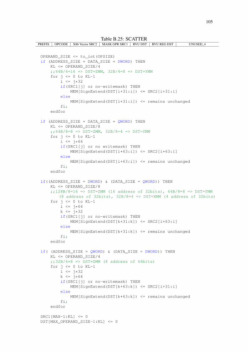
105
Table B.25: SCATTERPREFIX OPCODE X86 Vector SRC2 MASK GPR SRC1 RVU DST RVU REG DST UNUSED_4
OPERAND_SIZE <= to_int(OPSIZE)if (ADDRESS_SIZE = DATA_SIZE = DWORD) THEN
KL <= OPERAND_SIZE/4;;64B/4=16 => DST=ZMM, 32B/4=8 => DST=YMMfor j <= 0 to KL-1
i <= j*32if(SRC1[j] or no-writemask) THEN
MEM[SignExtend(DST[i+31:i]) <= SRC2[i+31:i]else
MEM[SignExtend(DST[i+31:i]) <= remains unchangedfi;
endfor
if (ADDRESS_SIZE = DATA_SIZE = QWORD) THENKL <= OPERAND_SIZE/8;;64B/8=8 => DST=ZMM, 32B/8=4 => DST=YMMfor j <= 0 to KL-1
i <= j*64if(SRC1[j] or no writemask) THEN
MEM[SignExtend(DST[i+63:i]) <= SRC2[i+63:i]else
MEM[SignExtend(DST[i+63:i]) <= remains unchangedfi;
endfor
if((ADDRESS_SIZE = DWORD) & (DATA_SIZE = QWORD)) THENKL <= OPERAND_SIZE/8;;128B/8=16 => DST=ZMM (16 address of 32bits), 64B/8=8 => DST=YMM
(8 address of 32bits), 32B/8=4 => DST=XMM (4 address of 32bits)for j <= 0 to KL-1
i <= j*64k <= j*32if(SRC1[j] or no-writemask) THEN
MEM[SignExtend(DST[k+31:k]) <= SRC2[i+63:i]else
MEM[SignExtend(DST[k+31:k]) <= remains unchangedfi;
endfor
if( (ADDRESS_SIZE = QWORD) & (DATA_SIZE = DWORD)) THENKL <= OPERAND_SIZE/4;;32B/4=8 => DST=ZMM (8 address of 64bits)for j <= 0 to KL-1
i <= j*32k <= j*64if(SRC1[j] or no-writemask) THEN
MEM[SignExtend(DST[k+63:k]) <= SRC2[i+31:i]else
MEM[SignExtend(DST[k+63:k]) <= remains unchangedfi;
endfor
SRC1[MAX-1:KL] <= 0DST[MAX_OPERAND_SIZE-1:KL] <= 0

106
Table B.26: VSHUF32x4PREFIX OPCODE RVU DST
RVUREG DST RVU SRC1
RVUREG SRC1
RVUSRC2
RVUREG SRC2 UNUSED_7 IMM_64 SRC3
Select16(SRC, control){CASE(control[3:0]) OF
0: TMP <= SRC[127:0]1: TMP <= SRC[255:128]. . .15: TMP <= SRC[2047:1920]
ESAC;RETURN TMP
Select8((SRC, control){CASE(control[2:0]) OF
0: TMP <= SRC[127:0]1: TMP <= SRC[255:128]. . .7: TMP <= SRC[1023:896]
ESAC;RETURN TMP
Select4((SRC, control){CASE(control[1:0]) OF
0: TMP <= SRC[127:0]1: TMP <= SRC[255:128]2: TMP <= SRC[383:256]3: TMP <= SRC[511:384]
ESAC;RETURN TMP
OPERAND_SIZE <= to_int(OPSIZE)KL <= OPERAND_SIZE/16if KL = 16 THEN
TMP_DST[127:0] <= Select16(SRC1[2048:0],imm64[3:0])TMP_DST[255:128] <= Select16(SRC1[2048:0],imm64[7:4]). . . . .TMP_DST[1919:1792] <= Select16(SRC1[2048:0],imm64[59:56])TMP_DST[2047:1920] <= Select16(SRC1[2048:0],imm64[63:60])
if KL = 8 THENTMP_DST[127:0] <= Select16(SRC1[2048:0],imm64[2:0])TMP_DST[255:128] <= Select16(SRC1[2048:0],imm64[5:3]). . . . .TMP_DST[895:768] <= Select16(SRC1[2048:0],imm64[20:18])TMP_DST[1023:896] <= Select16(SRC1[2048:0],imm64[23:21])
if KL = 4 THENTMP_DST[127:0] <= Select16(SRC1[2048:0],imm64[1:0])TMP_DST[255:128] <= Select16(SRC1[2048:0],imm64[3:2])TMP_DST[383:256] <= Select16(SRC1[2048:0],imm64[5:4])TMP_DST[511:384] <= Select16(SRC1[2048:0],imm64[7:6])
for j <= KL-1i <= j*32DEST[i+31:i] <= TEMP_DST[i+31:i]

107
Table B.27: VSHUF64x2PREFIX OPCODE RVU DST
RVUREG DST RVU SRC1
RVUREG SRC1
RVUSRC2
RVUREG SRC2 UNUSED_7 IMM_64 SRC3
Select16(SRC, control){CASE(control[3:0]) OF
0: TMP <= SRC[127:0]1: TMP <= SRC[255:128]. . .15: TMP <= SRC[2047:1920]
ESAC;RETURN TMP
Select8((SRC, control){CASE(control[2:0]) OF
0: TMP <= SRC[127:0]1: TMP <= SRC[255:128]. . .7: TMP <= SRC[1023:896]
ESAC;RETURN TMP
Select4((SRC, control){CASE(control[1:0]) OF
0: TMP <= SRC[127:0]1: TMP <= SRC[255:128]2: TMP <= SRC[383:256]3: TMP <= SRC[511:384]
ESAC;RETURN TMP
OPERAND_SIZE <= to_int(OPSIZE)KL <= OPERAND_SIZE/16if KL = 16 THEN
TMP_DST[127:0] <= Select16(SRC1[2048:0],imm64[3:0])TMP_DST[255:128] <= Select16(SRC1[2048:0],imm64[7:4]). . . . .TMP_DST[1919:1792] <= Select16(SRC1[2048:0],imm64[59:56])TMP_DST[2047:1920] <= Select16(SRC1[2048:0],imm64[63:60])
if KL = 8 THENTMP_DST[127:0] <= Select16(SRC1[2048:0],imm64[2:0])TMP_DST[255:128] <= Select16(SRC1[2048:0],imm64[5:3]). . . . .TMP_DST[895:768] <= Select16(SRC1[2048:0],imm64[20:18])TMP_DST[1023:896] <= Select16(SRC1[2048:0],imm64[23:21])
if KL = 4 THENTMP_DST[127:0] <= Select16(SRC1[2048:0],imm64[1:0])TMP_DST[255:128] <= Select16(SRC1[2048:0],imm64[3:2])TMP_DST[383:256] <= Select16(SRC1[2048:0],imm64[5:4])TMP_DST[511:384] <= Select16(SRC1[2048:0],imm64[7:6])
for j <= KL-1i <= j*32DEST[i+63:i] <= TEMP_DST[i+63:i]

108
Table B.28: PSHUFFLE_DPREFIX OPCODE RVU DST RVU REG DST RVU SRC1 RVU REG SRC1 UNUSED_2 Imm_64 SRC2
OPERAND_SIZE <= to_int(OPSIZE)
KL <= OPERAND_SIZE/4
FOR j <= 0 TO KL-1i <= j * 32
TMP_SRC[i+31:i] <= SRC[i+31:i]ENDFOR;
if(KL >= 4) then ;; RVU-16BTMP_DEST[31:0] <= (TMP_SRC[127:0] >> (ORDER[1:0] * 32))[31:0];TMP_DEST[63:32] <= (TMP_SRC[127:0] >> (ORDER[3:2] * 32))[31:0];TMP_DEST[95:64] <= (TMP_SRC[127:0] >> (ORDER[5:4] * 32))[31:0];TMP_DEST[127:96] <= (TMP_SRC[127:0] >> (ORDER[7:6] * 32))[31:0];if(KL >= 8) then ;; RVU-32BTMP_DEST[159:128] <= (TMP_SRC[255:128] >> (ORDER[1:0] * 32))[31:0];TMP_DEST[191:160] <= (TMP_SRC[255:128] >> (ORDER[3:2] * 32))[31:0];TMP_DEST[223:192] <= (TMP_SRC[255:128] >> (ORDER[5:4] * 32))[31:0];TMP_DEST[255:224] <= (TMP_SRC[255:128] >> (ORDER[7:6] * 32))[31:0];if(KL >= 16) then ;; RVU-64BTMP_DEST[287:256] <= (TMP_SRC[383:256] >> (ORDER[1:0] * 32))[31:0];TMP_DEST[319:288] <= (TMP_SRC[383:256] >> (ORDER[3:2] * 32))[31:0];TMP_DEST[351:320] <= (TMP_SRC[383:256] >> (ORDER[5:4] * 32))[31:0];TMP_DEST[383:352] <= (TMP_SRC[383:256] >> (ORDER[7:6] * 32))[31:0];TMP_DEST[415:384] <= (TMP_SRC[511:384] >> (ORDER[1:0] * 32))[31:0];TMP_DEST[447:416] <= (TMP_SRC[511:384] >> (ORDER[3:2] * 32))[31:0];TMP_DEST[479:448] <= (TMP_SRC[511:384] >> (ORDER[5:4] * 32))[31:0];TMP_DEST[511:480] <= (TMP_SRC[511:384] >> (ORDER[7:6] * 32))[31:0];if(KL >= 32) then ;; RVU-128BTMP_DEST[543:512] <= (TMP_SRC[641:512] >> (ORDER[1:0] * 32))[31:0];TMP_DEST[575:544] <= (TMP_SRC[641:512] >> (ORDER[3:2] * 32))[31:0];TMP_DEST[607:576] <= (TMP_SRC[641:512] >> (ORDER[5:4] * 32))[31:0];TMP_DEST[639:608] <= (TMP_SRC[641:512] >> (ORDER[7:6] * 32))[31:0];...TMP_DEST[927:896] <= (TMP_SRC[737:706] >> (ORDER[1:0] * 32))[31:0];TMP_DEST[959:928] <= (TMP_SRC[737:706] >> (ORDER[3:2] * 32))[31:0];TMP_DEST[991:959] <= (TMP_SRC[737:706] >> (ORDER[5:3] * 32))[31:0];TMP_DEST[1023:992] <= (TMP_SRC[737:706] >> (ORDER[7:6] * 32))[31:0];if(KL >= 64) then ;; RVU-256BTMP_DEST[1055:1024] <= (TMP_SRC[865:738] >> (ORDER[1:0] * 32))[31:0];TMP_DEST[1087:1056] <= (TMP_SRC[865:738] >> (ORDER[3:2] * 32))[31:0];TMP_DEST[1119:1088] <= (TMP_SRC[865:738] >> (ORDER[5:4] * 32))[31:0];TMP_DEST[1151:1120] <= (TMP_SRC[865:738] >> (ORDER[7:6] * 32))[31:0];...TMP_DEST[1953:1922] <= (TMP_SRC[2047:1920] >> (ORDER[1:0] * 32))[31:0];TMP_DEST[1983:1954] <= (TMP_SRC[2047:1920] >> (ORDER[3:2] * 32))[31:0];TMP_DEST[2015:1984] <= (TMP_SRC[2047:1920] >> (ORDER[5:3] * 32))[31:0];TMP_DEST[2047:2016] <= (TMP_SRC[2047:1920] >> (ORDER[7:6] * 32))[31:0];

109
Table B.29: VINSERT_HPREFIX OPCODE RVU DST
RVUREG DST RVU SRC1
RVUREG SRC1
RVUSRC2
RVUREG SRC2 UNUSED_7 IMM_8 SRC3
TEMP = SRC1case (SRC3[0])
0: TEMP[OPSIZE/2-1:0] <= SRC21: TEMP[OPSIZE: OPSIZE/2] <= SRC2
esac.
RVU_DST = TEMP
;; RVU_DST, RVU_SRC1 must be OPSIZE;; RVU_SRC2 must be OPSIZE/2
Table B.30: VEXTRACT_HPREFIX OPCODE RVU DST RVU REG DST RVU SRC1 RVU REG SRC1 UNUSED_2 Imm_8 SRC2
case(SRC3[0])0: TEMP = SRC1[OPSIZE/2-1:0]1: TEMP = SRC1[OPSIZE-1:OPSIZE/2]
esacRVU_DSL = TEMP
;; RVU_DST, RVU_SRC1 must be OPSIZE;; RVU_SRC2 must be OPSIZE/2

110
Table B.31: VINSERT_64x4PREFIX OPCODE RVU DST
RVUREG DST RVU SRC1
RVUREG SRC1
RVUSRC2
RVUREG SRC2 UNUSED_7 IMM_8 SRC3
TEMP = SRC1if(OPSIZE = 256B) then
case (SRC3[2:0])000: TEMP[255:0] <= SRC2001: TEMP[511:256] <= SRC2. . . . . . .111: TEMP[2047:1792] <= SRC2
esac.fi
if(OPSIZE = 128B) thencase (SRC3[1:0])
00: TEMP[255:0] <= SRC201: TEMP[511:256] <= SRC210: TEMP[767:512] <= SRC211: TEMP[1023:768] <= SRC2
esac.fi
if(OPSIZE = 64B) thencase (SRC3[0])
0: TEMP[255:0] <= SRC21: TEMP[511:256] <= SRC2
esac.fi
RVU_DST = TEMP

111
Table B.32: VEXTRACT_64x4PREFIX OPCODE RVU DST RVU REG DST RVU SRC1 RVU REG SRC1 UNUSED_2 Imm_8 SRC2
if(OPSIZE = 256B) thencase (SRC2[2:0])
000: TEMP <= SRC1[255:0]001: TEMP <= SRC1[512:256]. . . . . . .111: TEMP <= SRC1[2047:1792]
esac.fi
if(OPSIZE = 128B) thencase (SRC2[1:0])
00: TEMP <= SRC1[255:0]01: TEMP <= SRC1[511:256]10: TEMP <= SRC1[767:512]11: TEMP <= SRC1[1023:768]
esac.fi
if(OPSIZE = 64B) thencase (SRC2[0])
0: TEMP <= SRC1[255:0]1: TEMP <= SRC1[511:256]
esac.fi
RVU_DST = TEMP

112
APPENDIX C — OPCODE
OPCODE
PREFIX INSTRUCTION DATA TYPETABLE 5.3
OPSIZETABLE 5.2
8bits 8bits 3bits 5bits MNMONIC OBSERVATIONS
61h 00000000 000 4∼8192 LOAD_OPSIZE61h 00000000 001 4∼8192 LOAD_OPSIZE61h 00000000 010 4∼8192 LOAD_OPSIZE61h 00000000 011 4∼8192 LOAD_OPSIZE61h 00000000 100 4∼8192 LOAD_OPSIZE
61h 00000001 000 4∼8192 STORE_OPSIZE61h 00000001 001 4∼8192 STORE_OPSIZE61h 00000001 010 4∼8192 STORE_OPSIZE61h 00000001 011 4∼8192 STORE_OPSIZE61h 00000001 100 4∼8192 STORE_OPSIZE
61h 00000010 000 4∼8192 VADD_BYTE61h 00000010 001 4∼8192 VADD_WORD61h 00000010 010 4∼8192 VADD_DWORD61h 00000010 011 8∼8192 VADD_QWORD
61h 00000011 001 4∼8192 FVADD_WORD61h 00000011 010 4∼8192 FVADD_DWORD61h 00000011 011 8∼8192 FVADD_QWORD
61h 00000100 000 4∼8192 VSUB_BYTE61h 00000100 001 4∼8192 VSUB_WORD61h 00000100 010 4∼8192 VSUB_DWORD61h 00000100 011 4∼8192 VSUB_QWORD
61h 00000101 001 4∼8192 FVSUB_WORD61h 00000101 010 4∼8192 FVSUB_DWORD61h 00000101 011 4∼8192 FVSUB_QWORD
61h 00000111 000 4∼8192 VAND_BYTE61h 00000111 001 4∼8192 VAND_WORD61h 00000111 010 4∼8192 VAND_DWORD61h 00000111 011 4∼8192 VAND_QWORD
61h 00011111 000 4∼8192 VOR_BYTE61h 00011111 001 4∼8192 VOR_WORD61h 00011111 010 4∼8192 VOR_DWORD61h 00011111 011 4∼8192 VOR_QWORD
61h 00001000 000 4∼8192 VNOT_BYTE61h 00001000 001 4∼8192 VNOT_WORD61h 00001000 010 4∼8192 VNOT_DWORD61h 00001000 011 4∼8192 VNOT_QWORD

113
OPCODE
PREFIX INSTRUCTION DATA TYPETABLE 5.3
OPSIZETABLE 5.2
8bits 8bits 3bits 5bits MNMONIC OBSERVATIONS
61h 00001001 000 4∼8192 VSHIFTL_BYTE61h 00001001 001 4∼8192 VSHIFTL_WORD61h 00001001 010 4∼8192 VSHIFTL_DWORD61h 00001001 011 8∼8192 VSHIFTL_QWORD
61h 00001010 000 4∼8192 VSHIFTR_BYTE61h 00001010 001 4∼8192 VSHIFTR_WORD61h 00001010 010 4∼8192 VSHIFTR_DWORD61h 00001010 011 8∼8192 VSHIFTR_QWORD
61h 01001001 000 4∼8192 VSLLI_BYTE61h 01001001 001 4∼8192 VSLLI_WORD61h 01001001 010 4∼8192 VSLLI_DWORD61h 01001001 011 4∼8192 VSLLI_QWORD
61h 01001010 000 4∼8192 VSRLI_BYTE61h 01001010 001 4∼8192 VSRLI_WORD61h 01001010 010 4∼8192 VSRLI_DWORD61h 01001010 011 4∼8192 VSRLI_QWORD
61h 00001100 000 4∼8192 VMUL_BYTE61h 00001100 001 4∼8192 VMUL_WORD61h 00001100 010 4∼8192 VMUL_DWORD61h 00001100 011 8∼8192 VMUL_QWORD
61h 00001101 001 4∼8192 FVMUL_WORD61h 00001101 010 4∼8192 FVMUL_DWORD61h 00001101 011 8∼8192 FVMUL_QWORD
61h 00001110 000 4∼8192 VDIV_BYTE61h 00001110 001 4∼8192 VDIV_WORD61h 00001110 010 4∼8192 VDIV_DWORD61h 00001110 011 8∼8192 VDIV_QWORD
61h 00001111 001 4∼8192 FVDIV_WORD61h 00001111 010 4∼8192 FVDIV_DWORD61h 00001111 011 8∼8192 FVDIV_QWORD
61h 00010000 000 8∼8192 BROADCASTB61h 00010000 001 8∼8192 BROADCASTH61h 00010000 010 8∼8192 BROADCASTS61h 00010000 011 8∼8192 BROADCASTD

114
OPCODE
PREFIX INSTRUCTION DATA TYPETABLE 5.3
OPSIZETABLE 5.2
8bits 8bits 3bits 5bits MNMONIC OBSERVATIONS
61h 00010001 000 8∼8192 BROADCASTRB61h 00010001 001 8∼8192 BROADCASTRH61h 00010001 010 8∼8192 BROADCASTRS61h 00010001 011 8∼8192 BROADCASTRD
61h 00010010 000 4∼8192 VPERM_BYTE61h 00010010 001 8∼8192 VPERM_WORD61h 00010010 010 16∼8192 VPERM_DWORD61h 00010010 011 32∼8192 VPERM_QWORD
61h 00010011 000 4∼8192 VMOVV
61h 00010100 010 16∼64 VMOV_PIMtoM M = XMM, YMM, ZMM
61h 00100100 010 16∼64 VMOV_MtoPIM M = XMM, YMM, ZMM
61h 00010101 xxx 32∼256 VSHUFF32x4 No Multiple RVU Support
61h 00010110 xxx 32∼256 VSHUFF64x2 No Multiple RVU Support
61h 00011100 000 4∼8192 PSHUFFLE_BYTE61h 00011100 001 4∼8192 PSHUFFLE_WORD61h 00011100 010 4∼8192 PSHUFFLE_DWORD61h 00011100 011 4∼8192 PSHUFFLE_QWORD
61h 00010111 000 4∼8192 VXOR_BYTE61h 00010111 001 4∼8192 VXOR_WORD61h 00010111 010 4∼8192 VXOR_DWORD61h 00010111 011 4∼8192 VXOR_QWORD
61h 00011000 010 16∼64 VGATHER_DD61h 00011000 011 32∼128 VGATHER_DQ
61h 00011001 010 16∼32 VGATHER_QD61h 00011001 011 32∼64 VGATHER_QQ
61h 00011010 010 16∼64 VSCATTER_DD61h 00011010 011 32∼128 VSCATTER_DQ
61h 00011011 010 16∼32 VSCATTER_QD61h 00011011 011 32∼64 VSCATTER_QQ

115
OPCODE
PREFIX INSTRUCTION DATA TYPETABLE 5.3
OPSIZETABLE 5.2
8bits 8bits 3bits 5bits MNMONIC OBSERVATIONS
61h 00011101 000 4∼8192 VMIN_BYTE61h 00011101 001 4∼8192 VMIN_WORD61h 00011101 010 4∼8192 VMIN_DWORD61h 00011101 011 4∼8192 VMIN_QWORD
61h 00011110 001 4∼8192 FVMIN_WORD61h 00011110 010 4∼8192 FVMIN_DWORD61h 00011110 011 4∼8192 FVMIN_QWORD
61h 00111101 000 4∼8192 VMAX_BYTE61h 00111101 001 4∼8192 VMAX_WORD61h 00111101 010 4∼8192 VMAX_DWORD61h 00111101 011 4∼8192 VMAX_QWORD
61h 00111110 001 4∼8192 FVMAX_WORD61h 00111110 010 4∼8192 FVMAX_DWORD61h 00111110 011 4∼8192 FVMAX_QWORD
61h 01111100 010 64∼256 VINSERT64x4_DWORD61h 01111100 011 64∼256 VINSERT64x4_QWORD61h 01111101 010 64∼256 VEXTRACT64x4_DWORD61h 01111101 011 64∼256 VEXTRACT64x4_QWORD
No Multiple RVU Support
61h 01111110 010 64∼8192 VINSERTHALF_DWORD61h 01111110 011 64∼8192 VINSERTHALF_QWORD
61h 01111111 010 64∼8192 VEXTRACTHALF_DWORD61h 01111111 011 64∼8192 VEXTRACTHALF_QWORD

116
APPENDIX D — LIST OF LLVM MODIFIED FILES
The following files have been modified in LLVM to allow the proposed implemen-
tation. For informational purposes regarding the work to build PRIMO, around 20,000
lines of code have been entered into the LLVM.
• Middle-End - Vector Extension
/include/llvm/CodeGen/MachineValueType.h
/include/llvm/CodeGen/ValueTypes.td
/include/llvm/CodeGen/ValueTypes.h
/include/llvm/IR/Intrinsics.td
/lib/IR/ValueTypes.cpp
• Middle-End - Vector Size Selector
/lib/Transforms/Vectorize/LoopVectorize.cpp
• Back-end - Lane Extension
/lib/CodeGen/MIRParser/MIParser.cpp
/lib/CodeGen/RegisterCoalescer.cpp
/include/llvm/MC/LaneBitmask.h
/utils/TableGen/CodeGenRegisters.cpp
/utils/TableGen/RegisterInfoEmitter.cpp
• Back-end - Register File Definition
/lib/Target/X86/X86RegisterInfo.td
• Back-end - PIM Instruction Selection
/lib/Target/X86/X86ISelLowering.cpp
/lib/Target/X86/X86ISelLowering.h
/lib/CodeGen/SelectionDAG/SelectionDAG.cpp
/lib/Target/X86/X86InstrInfo.td
/lib/Target/X86/X86InstrInfo.cpp
/lib/Target/X86/X86InstrFormats.td

117
/lib/Target/X86/X86InstrFragmentsSIMD.td
/lib/Target/X86/X86Subtarget.cpp
/lib/Target/X86/X86Subtarget.h
/lib/Target/X86/X86.td
/lib/Target/X86/AsmParser/X86AsmParserCommon.h
/lib/Target/X86/AsmParser/X86Operand.h
/lib/Target/X86/Disassembler/X86Disassembler.cpp
/lib/Target/X86/Disassembler/X86DisassemblerDecoder.cpp
/lib/Target/X86/Disassembler/X86DisassemblerDecoderCommon.h
/lib/Target/X86/InstPrinter/X86ATTInstPrinter.cpp
/lib/Target/X86/InstPrinter/X86ATTInstPrinter.h
/lib/Target/X86/InstPrinter/X86IntelInstPrinter.cpp
/lib/Target/X86/InstPrinter/X86IntelInstPrinter.h
/utils/TableGen/X86RecognizableInstr.cpp