Embed Size (px)
Citation preview

EEL 4712 – Digital Design Test 2 – Spring Semester 2009 Name ___________________________________
1
IMPORTANT: • Please be neat and write (or draw) carefully throughout the test. If we cannot read it with a
reasonable effort, it is assumed wrong. • As always, the best answer gets the most points.
1. Miscellaneous. (a) Clock debouncing using a shift register and a clock divider
Design a switch debouncing circuit using a clock divider and a shift register (with an AND gate) with the following assumptions: • The bouncing period of a switch is determined to be 8 milli-seconds. • The system clock is 20 MHz • The clock divider is designed using 16 flip-flops.
What is the minimum number of flip-flops can be used for the shift register that will “cover” the bounding period of the switch?
(For credit, show work here.) _________________ (answer) (5 pts.)
(b) VGA display calculation:
10 pts.
Video_On
Horiz_Sync
Vert_Sync
Pixel information for 1 row (640 pixels)
Pixel information for 4 (of 480) rows [4 x 640 pixels]
1 Vert_Sync pulse for each screen refresh
1 Horiz_Sync pulse for each
row refresh (480rows per screen)
HSYNC_BEGIN
HSYNC_END
VSYNC_BEGIN
VSYNC_END
H_DISPLAY_END
etc.
Pixel information for 4 (of 480) rows [4 x 640 pixels]VSYNC END
hcount = 0 vcount = 0 here
D
B E
A
A = 37.77 uS B = 3.77 uS D = 25.17 uS E = 0.94 uS
For Lab 5, assuming the board clock frequency is 20 MHz, what constant should be use for HSYNC_END? For credit, please show work.
(For credit, show work here.) _________________ (answer) (5 pts.)

EEL 4712 – Digital Design Test 2 – Spring Semester 2009 Name ___________________________________
2
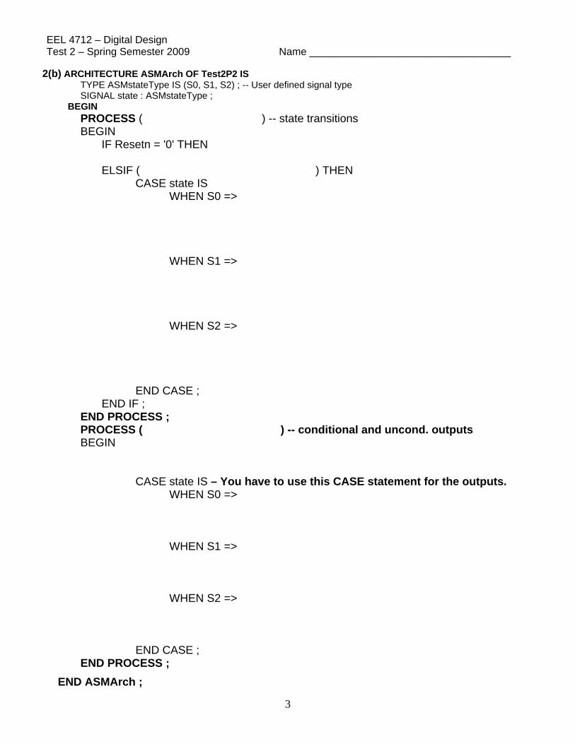
2. ASM/VHDL. Given below is a timing diagram (functional simulation) showing the desired timings among the states and signals of a controller.
(a) Construct an ASM diagram that will produce the above behavior. (8 pts.) (b) Complete the VHDL specification (on the next page) of your ASM diagram. Please don’t
change the structure of the code. In other words, you have to use the second CASE statement to implement the conditional and unconditional outputs. (10 pts.)
ENTITY Test2P2 IS PORT ( Clock, Resetn, InX : IN STD_LOGIC ; -- Resetn is active low, asynchronous OutY, OutZ : OUT STD_LOGIC ) ; END Test2P2;
18 pts.
S2 S2 S2 S2S1 S1 S0
EEL 4712 – Digital Design Test 2 – Spring Semester 2009 Name ___________________________________
3
2(b) ARCHITECTURE ASMArch OF Test2P2 IS TYPE ASMstateType IS (S0, S1, S2) ; -- User defined signal type SIGNAL state : ASMstateType ; BEGIN PROCESS ( ) -- state transitions BEGIN IF Resetn = '0' THEN ELSIF ( ) THEN CASE state IS WHEN S0 => WHEN S1 => WHEN S2 => END CASE ; END IF ; END PROCESS ; PROCESS ( ) -- conditional and uncond. outputs BEGIN CASE state IS – You have to use this CASE statement for the outputs. WHEN S0 => WHEN S1 => WHEN S2 => END CASE ; END PROCESS ;
END ASMArch ;

EEL 4712 – Digital Design Test 2 – Spring Semester 2009 Name ___________________________________
4
3. VHDL / ASM. Given the VHDL specification, draw the corresponding ASM chart. (Put ASM chart on the next page.)
ENTITY Prob3 IS PORT ( Clock, ResetA, ResetB, EN : IN STD_LOGIC ; RegLD, WE, SEL : OUT STD_LOGIC ) ; END Prob3 ;
ARCHITECTURE ASMArch OF Prob3 IS SIGNAL state : STD_LOGIC_Vector (1 DOWNTO 0); CONSTANT A : STD_LOGIC_Vector (1 DOWNTO 0):= "01"; CONSTANT B : STD_LOGIC_Vector (1 DOWNTO 0):= "11"; CONSTANT C : STD_LOGIC_Vector (1 DOWNTO 0):= "00"; CONSTANT D : STD_LOGIC_Vector (1 DOWNTO 0):= "10"; BEGIN PROCESS (state, ResetB, EN) BEGIN RegLD <= '0'; WE <= '0'; CASE state IS WHEN A => IF ResetB = '1' AND EN = '1' THEN RegLD <= '1'; END IF; WHEN B => RegLD <= '1'; WHEN C => RegLD <= '1'; IF ResetB = '0' AND EN = '1' THEN WE <= '1'; END IF; WHEN OTHERS => END CASE ; END PROCESS ; SEL <= '1' WHEN (state = “11”) OR (state = "00" AND ResetB = '0' AND EN = '0') ELSE '0'; PROCESS ( ResetA, Clock ) -- State transitions BEGIN IF ResetA = '0' THEN state <= B ; ELSIF (Clock'EVENT AND Clock = '1') THEN CASE state IS WHEN A => IF ResetB = '1' THEN state <= A ; ELSIF EN = '0' THEN state <= C; ELSE state <= “11” ; END IF ; WHEN B => IF ResetB = '1' THEN state <= A ; ELSE state <= “10”; END IF; WHEN “00” => IF ResetB = '1' THEN state <= A; ELSE state <= D; END IF ; WHEN D => state <= A; WHEN OTHERS => state <= A; END CASE ; END IF ; END PROCESS ;
17 pts.
END ASMArch ;

EEL 4712 – Digital Design Test 2 – Spring Semester 2009 Name ___________________________________
5
3. (Continued) (a) Put the ASM chart for Problem 3 here. (15 pts.)
(b) Is ResetA synchronous or asynchronous? (circle one) (1 pt.)
Is ResetB synchronous or asynchronous? (circle one) (1 pt.)

EEL 4712 – Digital Design Test 2 – Spring Semester 2009 Name ___________________________________
6
4. AltSynRam Problem
Complete the following timing diagram. Assume all flip-flops are initialized to ‘0’. Both RAM’s has the same data (ramdat.mif).
ramdat.mifDepth = 256; Width = 8; Address_radix = hex; Data_radix = hex; Content Begin 00 : 70; 07 : 77; 01 : 71; 08 : 78; 02 : 72; 09 : 79; 03 : 73; 0A : 7A; 04 : 74; 0B : 7B; 05 : 75; 0C : 7C; 06 : 76; etc.
17 pts.
Please put values in hex and an “X” where the value changes for SinglePortZ, aTrueDualZ, and bTrueDualZ.

EEL 4712 – Digital Design Test 2 – Spring Semester 2009 Name ___________________________________
7
5. FIR filter ASM problem
You are to design the controller of following component to fill the Input RAM for a Lab 6 FIR filter (from Location 0 to Location 256). Note that the Input RAM plays the same role as the Input ROM in Lab 6. • The controller will wait until it receives a RDY = ‘1’ from the Lab 6 FIR filter, then it will
proceed to fill the Input RAM. • It will check to see if the FIFO is empty
• If empty = ‘1’, it will wait. • If empty = ‘0’,
• It will request a 32-bit value from the FIFO (set rdreq = ‘1’). The next value in the FIFO will be outputed from the FIFO q[31..0] at the next active clock transition.
• This value should be written into the next location in the Input RAM. • This will be done until the Input RAM is full (256 locations), each time making sure the
FIFO is not empty. • When finished, it will signal the Lab 6 FIR filter by setting Start = ‘1’ and return to the Wait
state. Note: Function of the FIFO: • rdreq:
• 0: The output q[31..0] will hold the last value outputted from the FIFO. • 1: The next value in the FIFO will be outputed from the FIFO q[31..0] at the next active
clock transition. • empty:
• 0: The FIFO is not empty (there are some values in it). • 1: The FIFO is empty.
This simple dual-port RAM replaces the Input ROM in Lab 6 to produce Input[31..0] to FIR Filter.
FIFO
Input [31..0]
Other Controller
Inputs
clock
ControllerController Outputs
Lab 6 FIR
Filter
RDY
Start
Connected to Lab 6 FIR Filter
Used by other
component
Address Generator
wradddress CtrCLR
CtrEN
Synchronous: • CLR clears counter • EN increments counter
20 pts.

EEL 4712 – Digital Design Test 2 – Spring Semester 2009 Name ___________________________________
8
5. continued (a) Complete the block diagram of the Controller, specifying all the Controller inputs and
Controller outputs. (4 pts.) (b) Put the ASM chart for the Controller here. (16 pts.)

EEL 4712 – Digital Design Test 2 – Spring Semester 2009 Name ___________________________________
9
6. FIR filter Datapath component, using GENERATE statement (a) Shown on the next page is the example code that we discussed in class. Modify the code to make it
into a set of 32 multipliers. You can make the changes right on the code on the next page. (6 pts.)
• You can assume that coeff(32 DOWNTO 1) have been defined and assigned for you to use.
(b) Assume that we want to complete the 32-bit Datapath component, give me the code required to implement the required 32-bit shift registers to produce reg(32 DOWNTO 1). (6 pts.)
• Restriction: You cannot use PORT MAP statements for this part. (Hint: PROCESS statement)
(Put your answer here, including any new TYPE or SIGNAL definitions)
(c) Continuing with the 32-bit Datapath component, give me the code required to implement the NEXT level of adders (i.e., you don’t have to implement the other levels of adders). (6 pts.)
• Restriction: This time, you have to GENERATE and PORT MAP statements for this part.
(Put your answer here, including any new TYPE or SIGNAL definitions)
18 pts.

EEL 4712 – Digital Design Test 2 – Spring Semester 2009 Name ___________________________________
10
-- snippet of code to demonstrate Multi-dimensional arrays and GENERATE statement ARCHITECTURE struct OF datapath IS -- Definition of other components COMPONENT multiplier IS PORT ( clock : IN STD_LOGIC; dataa : IN STD_LOGIC_VECTOR(31 DOWNTO 0); datab : IN STD_LOGIC_VECTOR(31 DOWNTO 0); result: OUT STD_LOGIC_VECTOR(31 DOWNTO 0) ); END COMPONENT; COMPONENT adder IS PORT ( clock : IN STD_LOGIC ; dataa : IN STD_LOGIC_VECTOR (31 DOWNTO 0); datab : IN STD_LOGIC_VECTOR (31 DOWNTO 0); result : OUT STD_LOGIC_VECTOR (31 DOWNTO 0) ); END COMPONENT; SUBTYPE signalVectors IS STD_LOGIC_VECTOR(31 DOWNTO 0); TYPE array4OfSignals IS ARRAY(4 DOWNTO 1) OF signalVectors; TYPE array5OfSignals IS ARRAY(5 DOWNTO 1) OF signalVectors; SIGNAL coeff: array32OfSignals; -- You can assume that coeff(32 DOWNTO 1) have -- been defined and assigned for you to use. SIGNAL reg: array5OfSignals; -- reg(4 DOWNTO 1) are outputs of the 4 registers -- reg(5) is the input to the left-most registers SIGNAL mout: array4OfSignals; BEGIN -- shift register code mults: FOR i IN 1 to 4 GENERATE multArray : multiplier PORT MAP (clock=>clk, dataa=>coeff(i), datab=>reg(i), result=>mout(i)); END GENERATE mults;
-- code for adders
END struct;

EEL 4712 – Digital Design Test 2 – Spring Semester 2009 Name ___________________________________
11
ENTITY _entity_name IS PORT(__input_name, __input_name : IN STD_LOGIC; __input_vector_name : IN STD_LOGIC_VECTOR(__high downto __low); __bidir_name, __bidir_name : INOUT STD_LOGIC; __output_name, __output_name : OUT STD_LOGIC); END __entity_name; ARCHITECTURE a OF __entity_name IS SIGNAL __signal_name : STD_LOGIC; SIGNAL __signal_name : STD_LOGIC; BEGIN -- Process Statement -- Concurrent Signal Assignment -- Conditional Signal Assignment -- Selected Signal Assignment -- Component Instantiation Statement END a; __instance_name: __component_name PORT MAP (__component_port => __connect_port, __component_port => __connect_port); WITH __expression SELECT __signal <= __expression WHEN __constant_value, __expression WHEN __constant_value, __expression WHEN __constant_value, __expression WHEN __constant_value; __signal <= __expression WHEN __boolean_expression ELSE __expression WHEN __boolean_expression ELSE __expression; IF __expression THEN __statement; __statement; ELSIF __expression THEN __statement; __statement; ELSE __statement; __statement; END IF; CASE __expression IS WHEN __constant_value => __statement; __statement; WHEN __constant_value => __statement; __statement; WHEN OTHERS => __statement; __statement; END CASE; WAIT UNTIL __expression;
<generate_label>: FOR <loop_id> IN <range> GENERATE -- Concurrent Statement(s) END GENERATE;
EEL 4712 – Digital Design Test 2 – Spring Semester 2009 Name ___________________________________
12
IMPORTANT: • Please be neat and write (or draw) carefully. If we cannot read it with a reasonable effort, it is
assumed wrong. • As always, the best answer gets the most points.
COVER SHEET:
Problem: Points:
1 (10 pts)
2 (18 pts)
3 (17 pts)
4 (17 pts)
5 20 pts)
6. (18 pts)
Re-Grade Information:
_______________________________________________________________________
_______________________________________________________________________
_______________________________________________________________________
_______________________________________________________________________
_______________________________________________________________________
_______________________________________________________________________
_______________________________________________________________________
_______________________________________________________________________
_______________________________________________________________________
_______________________________________________________________________
_______________________________________________________________________
_______________________________________________________________________
Total