Embed Size (px)
Citation preview
Implementing An LCD Interface In A Customizable ARM7 Microcontroller
Using The CAP7 Metal Programmable Block

222Confidential
APB
ICE
AMBA Bridge
ARM7TDMIPIT
MainOSC
PLL
PMC WDTPLL
6-layer AHB Matrix
JTAG
Peripheral DMAController
AIC
USART ADCTimerx3 USARTPIO
x64
SRAM96KB
MPLIB250K/450K ASIC gates
EBI
Static Mem.CF
NAND FlashSDRAM
ROM (256KB)
SPI
RTT
SHWDC GPBREGPOR
32K OSCRC OSC
USBFS
Device
SRAM64KB
POR
What is CAP7?
333Confidential
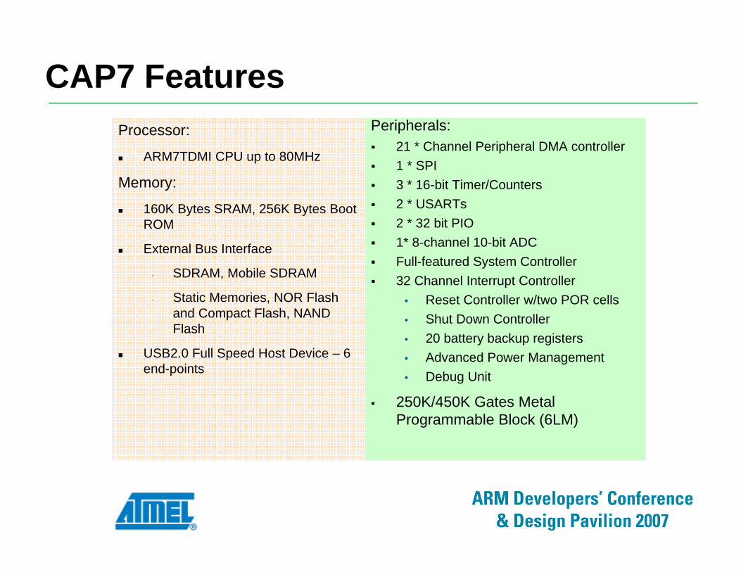
Processor:
ARM7TDMI CPU up to 80MHz
Memory:
160K Bytes SRAM, 256K Bytes Boot ROM
External Bus Interface
- SDRAM, Mobile SDRAM
- Static Memories, NOR Flash and Compact Flash, NAND Flash
USB2.0 Full Speed Host Device – 6 end-points
Peripherals:21 * Channel Peripheral DMA controller1 * SPI3 * 16-bit Timer/Counters2 * USARTs2 * 32 bit PIO 1* 8-channel 10-bit ADCFull-featured System Controller32 Channel Interrupt Controller
• Reset Controller w/two POR cells• Shut Down Controller• 20 battery backup registers• Advanced Power Management • Debug Unit
250K/450K Gates Metal Programmable Block (6LM)
CAP7 Features

444Confidential
Application: Adding An LCD Interface
555Confidential
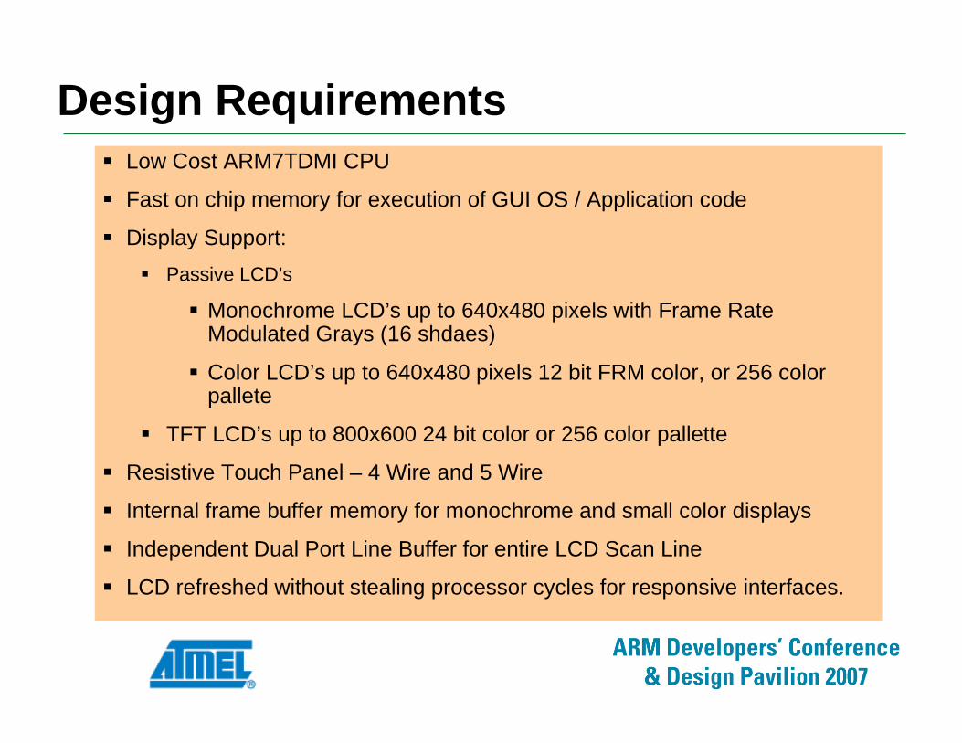
Low Cost ARM7TDMI CPU
Fast on chip memory for execution of GUI OS / Application code
Display Support:Passive LCD’s
Monochrome LCD’s up to 640x480 pixels with Frame Rate Modulated Grays (16 shdaes)
Color LCD’s up to 640x480 pixels 12 bit FRM color, or 256 color pallete
TFT LCD’s up to 800x600 24 bit color or 256 color pallette
Resistive Touch Panel – 4 Wire and 5 Wire
Internal frame buffer memory for monochrome and small color displays
Independent Dual Port Line Buffer for entire LCD Scan Line
LCD refreshed without stealing processor cycles for responsive interfaces.
Design Requirements

666Confidential
LCD Refresh Consumes The Bus
ARM7 CPUApplication Code
And Data
Display Frame Buffer
640x480 = 1,228,800 Bytes
Memory
LCD Controller
Display Refresh = 1.2 MBytes @ 60 Hz = 73,728,000 bytes/second

777Confidential
Concurrent Execution and LCD Refresh
ARM7 CPU
On Chip Memory
Application Code
And Data
External Memory
Frame Buffer640x480 =
1,228,800 Bytes
LCD Controller

888Confidential
LCD Usage of CAP7 Resources
APB
ICE
AMBA Bridge
ARM7TDMI
6-layer AHB Matrix
JTAG
Peripheral DMAController
USART ADCTimerx3 USARTPIO
x64
SRAM(96KB)
EBI
Static Mem.
SDRAM
ROM(256KB)
SPIUSBFS
Device
SRAM(64KB)
PIXEL FormatterExternal
RAM
Frame Buffer
LineBuffer(DualPort)
Color Pallete(DualPort)
AHB MASTER 1
LCD Timing Generator
AHB MASTER 2
ControlRegisters
999Confidential
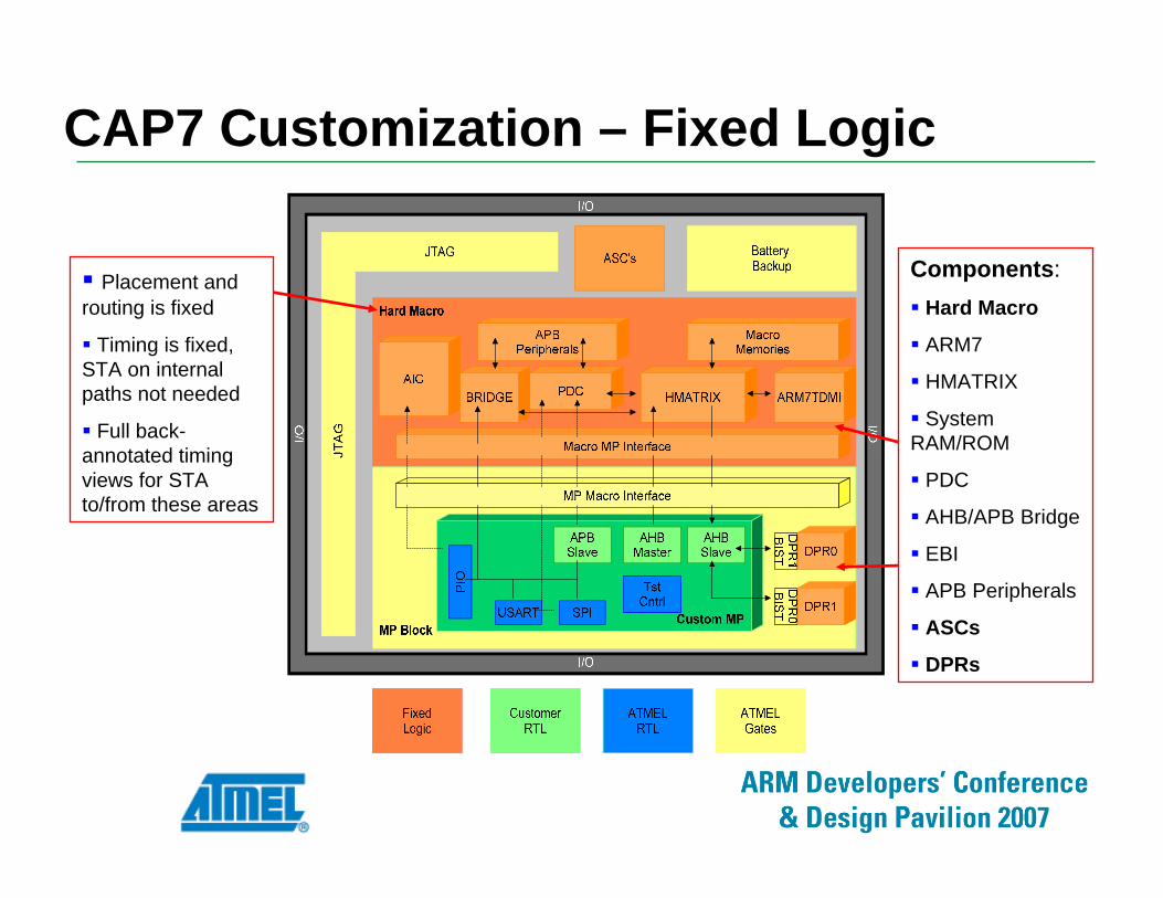
Components:Hard Macro
ARM7
HMATRIX
System RAM/ROM
PDC
AHB/APB Bridge
EBI
APB Peripherals
ASCs
DPRs
Placement and routing is fixed
Timing is fixed, STA on internal paths not needed
Full back-annotated timing views for STA to/from these areas
CAP7 Customization – Fixed Logic

101010Confidential
Delivered a pre-synthesized gates
Design Centers will need to place, route, and extract timing
Gives freedom to customize* (within restrictions)
In most cases, customer can used as delivered
Components:
Battery Backup
JTAG logic
MP Macro Interface
DPR BIST
* This is not part of the default quick turn flow
CAP7 Customization – Atmel Gates

111111Confidential
Components:
Custom MP
Area designated for the customer’s logic
CAP7 Customization – Customer RTL

121212Confidential
Components:
Atmel IPIP from Atmel to
be used directly by the customer
Delivered as protected RTL, gates*
Design centers will need to assist customers for integration
* Available views will depend on IP
CAP7 Customization – Atmel RTL

131313Confidential
Components:
Digital I/OI/O placement is
fixed
I/O sites can be customized* in metal to change drive strengths, pullup/pulldown/bus holder.
MP I/O sites can be converted in additional power/gnd pads if needed*
* This is not part of the default quick turn flow
CAP7 Customization – I/O

141414Confidential
MP Block 4x4 AHBSlaves
4 AHBMasters
Clock (42)
ITs (19)
13 PDC channels
MPIOs
(90)
USB PHY
DPR
2kx16
DPR
2kx16
ChipID
Resets (4)
Chip Boundary Scan
MPBlock Custom AREA
450K Gates
Ext ChipID
15 APB Slaves
. . .
. . . MP Interface – Scan Wrapper
BIST
B
IST
The USB transceiver cell can be utilized by the customer to implement their own USB host or device
DPR memories are completely for customer use. BIST is provided
4x4 AHB Slaves and 4 AHB Masters are connected to the MBBlock
90 MPIO I/OS
MP I/Os type may be customized
MPBlock scan chain wrapper for Chip and MPBlock scan test
- Clocks from APMC and APB bridge- Interrupts to AIC- APB Peripherals to Hard Macro Bridge and PDC
15 APB Slaves available to the MPBlock
MP Interface Wrapper and BIST are located in the MP area so actual gates available to the customer will be less than 450K
CAP7 MP Block Interface

151515Confidential
Place & Route (Metal Layers)
Integration
Prototype Fabrication
Production Volume
System Prototyping
10~12 WEEKS
CAP7 Design Flow

161616Confidential
Emulation Platform
Custom
IP Blocks
CAP9
Or CAP7 FPGA
Emulate your future device in a few weeks
Model your custom IP
Test your software on target hardware
CAP7 Emulation Strategy

171717Confidential
One motherboard supporting either CAP7 or CAP9 daughtercards(Altera-based and Xilinx-based versions to be available for either CAP device)Design to support LCD, audio, PIO, communications interface, etc.Design to facilitate OS supportSupports different EBI memory typesLow cost solution
CAP Emulation Board
181818Confidential
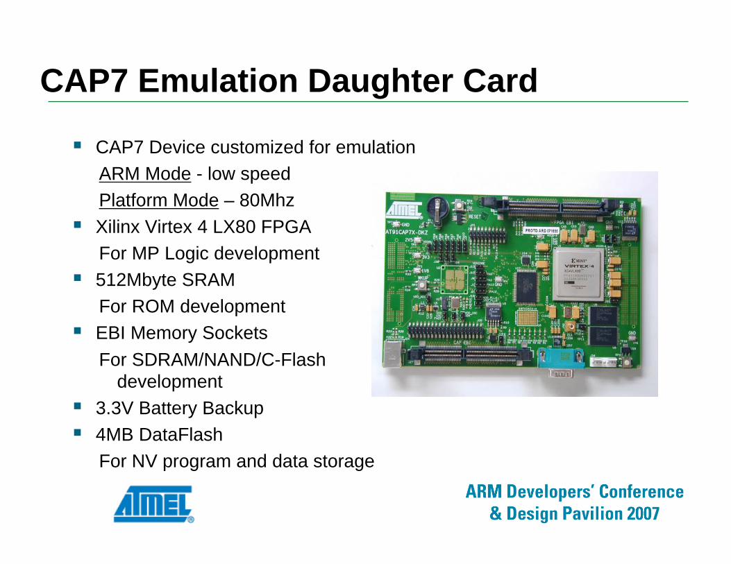
CAP7 Device customized for emulationARM Mode - low speedPlatform Mode – 80MhzXilinx Virtex 4 LX80 FPGAFor MP Logic development512Mbyte SRAMFor ROM developmentEBI Memory SocketsFor SDRAM/NAND/C-Flash
development3.3V Battery Backup4MB DataFlashFor NV program and data storage
CAP7 Emulation Daughter Card

191919Confidential
MP Logic RTL Synthesis Netlist P & R Bitstream
Veri log/VHDL .edf
C/C++ ICE
.mpm
0100111001110010101011110010101111000...
Func Sims *
Post-Layout Sims *
Simulators Supported
NC Verilog/ Modelsim
Source Compile/Link/Debug Download/ICE .Hex
*
H/W Flow
S/W Flow
CAP7L
SRAM
Xi l inx Platform Flash
JTAG ICE Header
USB Ethernet
Push Buttons Swi tch
JTAG Header
Product #
Rev. A UART 0 UART 1
LED's
Header
Header
Header
Hea
der
Xilinx Virtex 4LX60
EBI Interface Daughtercard Connector EBI Interface Daughtercard Connector
emulation personali ty
CAP7 Emulation Design Flow Summary

202020Confidential
Designers code their MP Logic module in HDL and synthesize1 to an .edf FPGA gate-level netlistFPGA compiler tools1 are used to combine the user’s MP logic block netlist with the CAP7 platform netlistAtmel provided macro files handle merging of both netlists, P&R, and generation of the FPGA bitstreamA vendor-supplied JTAG-ISP tool is used to program the FPGA configuration PROM with the bitstream
1Xilinx ISE tools include XST for synthesisAltera Quartus support Nov-07
MP Logic Block Development
212121Confidential
Supported with Cadence NC Verilog or Mentor ModelsimAtmel Provides:
ARM7TDMI Solaris/Linux compatible modelEncrypted Verilog model of CAP7 platform logicScripts to support simulation environment (e.g. makefiles, Perl, etc.)Verilog testbench
FPGA RTL Functional Simulation

222222Confidential
Supported with Cadence NC Verilog or Mentor ModelsimAtmel Provides:
ARM7TDMI Solaris/Linux compatible modelFPGA netlist for CAP7 Platform LogicScripts to support simulation environment (e.g. makefiles, Perl, etc.)Verilog testbench (same as for RTL simulations)
FPGA Post-Layout Simulations

232323Confidential
Vendors :ARM ADSGNU GCC + EclipseIAR Embedded WorkbenchGreen Hills Multi IDE Keil RealView MDK Rowley CrossWorks
+
S/W Tool Chain Environment