Embed Size (px)
Citation preview

IMPLEMENTING A PIEZOELECTRIC TRANSFORMER FOR A
FERROELECTRIC PHASE SHIFTER CIRCUIT
ANTHONY M. ROBERTS
Bachelor of Electrical Engineering
Cleveland State University
May, 2008
Submitted in partial fulfillment of requirements for the degree
MASTER OF SCIENCE IN ELECTRICAL ENGINEERING
at the
CLEVELAND STATE UNIVERSITY
December, 2011

This thesis has been approved
for the Department of Electrical and Computer Engineering
and the College of Graduate Studies by
________________________________________________
Thesis Committee Chairperson, Dr. Fuquin Xiong
________________________________
Department/Date
________________________________________________
Dr. Robert Romanofsky
________________________________
Department/Date
________________________________________________
Dr. Ana Stankovic
________________________________
Department/Date
________________________________________________
Dr. Nigamanth Sridhar
________________________________
Department/Date

DEDICATION
To the glory of the Lord Jesus Christ, through who’s love I have been so blessed.

ACKNOWLEDGEMENTS
For all this work and everything wonderful it has brought into my life, I owe Dr.
Bob Romanofsky a debt of gratitude I can never repay. As a mentor he has given me
invaluable guidance on research, my career, and life. His own work and accomplishments
are an inspiration and motivate me to continue learning and always seek out new
opportunities. I am grateful for his friendship, because as long as I “love NASA and the
space program and humanity” he’ll always be in my corner.
There is no greater comfort that the love of my parents and that they have
been, and will be, there for me. My achievements are their achievements.
Many thanks to the staff of NASA Glenn whose technical help and
company I have come to appreciate so much. Many thanks to Liz Mcquaid, Fred Van
Keuls, Max Scardeletti, Nick Varaljay, and George Ponchak.
I owe much to the faculty and staff at Cleveland State University’s
Department of Electrical and Computer Engineering for the time, patience, help, and lab
resources that allowed me to accomplish this work.
A special thanks to Alicia Pavlecky for reviewing my grammar and style.
A very special thanks to Bill Witt and Joe Rymut. Whether it was
badgering me to finish my work, your guaranteed willingness to go out for beer, or
providing a relieving distraction, you were there. Good friends like these are far and few
between.
Thanks be to God, through whom all things are possible.

v
IMPLEMENTING A PIEZOELECTRIC TRANSFORMER FOR A
FERROELECTRIC PHASE SHIFTER CIRCUIT
ANTHONY ROBERTS
ABSTRACT
The ferroelectric phase shifter is the fundamental component in a new type of
scanning phased array, the ferroelectric reflectarray. These phase shifters require a DC
bias voltage, up to 300 Vdc, for continuous 0 to 360 degree phase shift. In a conventional
phased array comprised of potentially thousands of phase shifters, each phase shifter
requires up to six control signals so routing and integration become extremely complex.
The coplanar ferroelectric phase shifters require only a single control signal, albeit at high
voltage. If a technology could be developed that allows a low-level signal to be routed to
each phase shifter and converted to the proper bias voltage levels, essentially at the phase
shifter, then a new type of phased array architecture could be realized.
Magnetic circuit components comprise a conventional means for voltage and
current step-up and step-down. However, magnetic devices suffer from resistive (I2R)
losses, and dimensional and economical costs, thereby forcing compromises in design

vi
and cost. Integrated multichannel, high voltage amplifiers have been developed for the
MEMs industry and are usually based on high voltage Op Amp arrays. The goal of this
work, however, is to demonstrate low power, high voltage control to complement the
inherent high efficiency of the ferroelectric reflectarray.
This research explores using a piezoelectric transformer (PT) as the alternative
enabling component in the voltage supply for a ferroelectric phase shifter utilizing
piezoelectrics in an AC-DC converter. Unlike magnetic transformers PTs generate no
electromagnetic interference, have higher efficiencies, and have higher power densities.
Preliminary work consisted of characterizing the device under cryogenic
conditions due to the temperature-dependant dielectric constant of ferroelectrics and
ultimately realistic environmental conditions. Then an analysis of the equivalent PT
model is performed focusing on reconciling the theoretical results with the experimental
and extracting the equivalent circuit parameters for the point of operation. Next, in a
proof-of-concept application, a circuit was developed for using the PT in a driver for a
ferroelectric phase shifter.
Initial results were successful with the driver achieving an output voltage from 0
to over 400 Vdc while accomplishing 0 to 115 degrees phase shift at Ka-band frequencies
(phase shift was limited to less than a full 2π because of phase shifter design).
Future work includes, further characterizing the piezoelectric transformer,
improving the driver circuit, implementing an output voltage feedback control scheme,
and using the driver in a ferroelectric phased array antenna.

vii
TABLE OF CONTENTS
Page
ABSTRACT……………………………………………………………………………...V
NOMENCLATURE ...................................................................................................... XII
LIST OF TABLES .......................................................................................................... IX
LIST OF FIGURES ......................................................................................................... X
I INTRODUCTION ........................................................................................................ 1
1.1 Background ....................................................................................................... 1
1.2 Problem Formulation ...................................................................................... 21
1.3 Thesis Organization ........................................................................................ 22
II CHARACTERIZING THE MLPT ......................................................................... 24
2.1 Motivation ....................................................................................................... 24
2.2 Experimental Characterization: Procedure and Results .................................. 27
III PT MODELING AND SIMULATION ................................................................. 43
3.1 Overview ......................................................................................................... 43
3.2 Static Operation .............................................................................................. 45
3.3 Dynamic Operation ......................................................................................... 52

viii
IV DRIVER CIRCUIT DESIGN ................................................................................. 56
4.1 Theory of Operation and Design..................................................................... 56
4.2 Prototype Performance Evaluation ................................................................. 60
4.3 Integration with the Ferroelectric Phase Shifter ............................................. 63
V CONCLUSION.......................................................................................................... 67
5.1 Summary ......................................................................................................... 67
5.2 Future Research and Work.............................................................................. 69
REFERENCES ................................................................................................................ 73
APPENDIX ...................................................................................................................... 75

ix
LIST OF TABLES
Table Page
Table 1: Characteristics for the SMMTF53P2S40 Piezoelectric Material ..................................... 18
Table 2: PT Equivalent Component Values ................................................................................... 49
Table 3: PT Equivalent Component Experimental Values ............................................................ 50
Table 4: PT Equivalent Component Curve-Fitting Results ........................................................... 51

x
LIST OF FIGURES
Figure Page
Figure 1: X-band Ferroelectric Reflectarray .................................................................................... 2
Figure 2: Thin Film Ferroelectric Phase Shifter .............................................................................. 3
Figure 3: Crystal Lattice Cell of BaTiO3 ......................................................................................... 5
Figure 4: Deformation of Cell Followed by Polarization ................................................................ 5
Figure 5: The 616 Element Reflectarray Controller Connected to the Reflectarray ........................ 7
Figure 6: Element Controller with High Voltage Switching IC ...................................................... 8
Figure 7: Lead Zirconate Titanate Elementary Cell ......................................................................... 9
Figure 8: Piezoelectric Poling in Weiss Domains .......................................................................... 10
Figure 9: Designation of the Axes and Directions of Deformation ............................................... 11
Figure 10: A Rosen-type Piezoelectric Transformer ..................................................................... 15
Figure 11: Equivalent Circuit Model for the Piezoelectric Transformer ....................................... 17
Figure 12: Mechanical Drawings for the SMMTF53P2S40 Multilayer PT................................... 19
Figure 13: Cryostat and Instrumentation ....................................................................................... 28
Figure 14: PT Setup for Cryogenic Testing ................................................................................... 29
Figure 15: PT Frequency Response at 298 K ................................................................................ 30
Figure 16: PT Cryogenic Frequency Response.............................................................................. 31
Figure 17: PT Cryogenic Split Resonance Frequency Response ................................................... 33
Figure 18: PT Input Impedance Magnitude ................................................................................... 35
Figure 19: PT Input Impedance Phase Angle ................................................................................ 36
Figure 20: LR200 Coherent Laser Radar. ...................................................................................... 38
Figure 21: Dimension Measurement Results ................................................................................. 38
Figure 22: Experimental and Simulated (Mnfr.) Frequency Responses ........................................ 46
Figure 23: Experimental and Simulated (Mnfr.) Frequency Responses (Tuned) .......................... 47

xi
Figure 24: Experimental and Simulated (Exp.) Frequency Responses .......................................... 48
Figure 25: Experimental and Simulated (Exp.) Frequency Responses (Tuned) ............................ 48
Figure 26: Curve fitting Frequency Response ............................................................................... 50
Figure 27: PT Gain as a Function of n ........................................................................................... 53
Figure 28: Input Impedance Magnitude as a Function of n ........................................................... 54
Figure 29: Complete schematic for proof-of-concept driver circuit .............................................. 58
Figure 30: Complete Phase Shifter Driver Circuit ......................................................................... 60
Figure 31: Driver Circuit Voltage Output For Fixed Fin and Variable Vin .................................. 61
Figure 32: Driver Circuit Voltage Output for Fixed Vin and Variable Fin ................................... 62
Figure 33: Fin = 42.79 kHz, 0.1 Vdc Applied, 139.21 Degrees Phase Shift Result ...................... 64
Figure 34: Fin = 46.01 kHz, 1.0 Vdc Applied, 139.39 Degrees Phase Shift Result ...................... 64
Figure 35: Fin = 50.48 kHz, 10.0 Vdc Applied, 144.98 Degrees Phase Shift Result .................... 65
Figure 36: Fin = 52.21 kHz, 50.0 Vdc Applied, 165.71 Degrees Phase Shift Result .................... 65
Figure 37: Fin = 52.82 kHz, 100.0 Vdc Applied, -179.24 Degrees Phase Shift Result ................. 66
Figure 38: Fin = 53.46 kHz, 300.0 Vdc Applied, -123.10 Degrees Phase Shift Result ................. 66
Figure 39: Coupled Mass-Spring-Damper System ....................................................................... 75
Figure 40: PT Dual-Resonance Time Domain Response .............................................................. 77
Figure 41: PT Dual-Resonance Frequency Domain Response ...................................................... 77
Figure 42: Equivalent Electrical Circuit ........................................................................................ 78

xii
NOMENCLATURE
DC: Direct current
AC: Alternating current
Vdc: Direct current volts
Vac: Alternating current volts
V/V: Volts per Volt
PT: Piezoelectric transformer
IC: Integrated circuit
RTD: Resistance temperature detector
MLPT: Multilayer piezoelectric transformer
GBP: Gain bandwidth product

1
CHAPTER I
INTRODUCTION
1.1 Background
A phased array is a type of antenna made electronically steerable by means of
constructive and destructive interference from electromagnetic waves emitted by multiple
elements on the antenna. Its surface is composed of many phase shifters that become
active with a certain phase delay. It is this delay between the phase shifters that facilitates
the interference pattern necessary to steer the beam. The range of frequencies for which
the antenna operates determines the details of its construction. The advantages of the
phased array over a gimbaled parabolic antenna are the elimination of moving parts, rapid
beam steering, better integration, and packaging flexibility [1].

2
Figure 1: X-band Ferroelectric Reflectarray
The reflectarray is an improvement being pioneered at NASA’s Glenn Research
Center by Dr. Robert Romanofsky. It is a phased array antenna (Figure 1) but with the
directly radiating array replaced by a feed horn that illuminates a reflective surface in
transmission and collects the reflections off the surface in the receiving mode [2]. The
novelty of this application is in the elements that make up the reflectarray surface and
accomplish the beam steering. In a conventional phased array, the phase shifters are
located between the amplifiers and radiating elements. A modulated signal from a single
source is distributed to the phase shifters through some type of manifold. This type of
array is called direct radiating. The phase shifter loss is unimportant because the phase
shifters follow the low noise amplifiers in the case of a receiving array and precede the
power amplifiers in the case of a transmitting array. Consequently they do not play a part
in determining the sensitivity or noise temperature in the former, nor do they significantly
affect efficiency in the latter. In a reflectarray, the phase shifters are located between the
amplifier and the radiators, therefore they determine sensitivity and efficiency, and their
insertion loss is of paramount importance. Conventional commercial monolithic
microwave integrated circuit phase shifters have an insertion loss approaching or

3
exceeding 10 dB at Ka-band, rendering a reflectarray with such devices impractical.
NASA Glenn has developed low loss phase shifters based on thin ferroelectric films, an
example of which is shown in Figure 2. This device is the motivation behind this
research.
Figure 2: Thin Film Ferroelectric Phase Shifter
1.1.1 Ferroelectrics and the Phase Shifter
Ferroelectrics are crystals that electrically polarize under the influence of a strong
electric field. Ferroelectricity is analogous to ferromagnetism in ferromagnetic materials.
When the external electric field is removed, some of the crystals in the substance retain
their polarization. If enough of the crystals have done so then the mass as a whole retains
an electric polarization. If a field were applied in the opposite direction, with the intent of
reversing the bulk ferroelectric’s polarization, then energy would first have to be
expended in reversing the previously biased crystals before the bulk material as a whole
could be polarized. This behavior manifests itself as hysteresis in the ferroelectric
material. Once the bulk substance is polarized it saturates. Any further increase in the

4
external electric field results in no further of an effect, much like saturation in a magnetic
core. It is this hysteresis, the retention of electric polarization, which is characteristic of
ferroelectrics [3]. Ferroelectrics are excellent dielectrics, with dielectric constants in the
hundreds for many crystal types. When a ferroelectric crystal is heated past its Curie
temperature (a temperature unique to each particular crystal), it enters the paraelectric
region and becomes non-polar because the crystal cell assumes a symmetrical shape.
Also at this temperature, the dielectric constant increases to the thousands. When the
crystal cools through its Curie temperature, it (and the bulk material specifically) forms
Weiss domains. Typically in the bulk ferroelectric material, groups of crystals form
regions which behave as a single crystal. Known as Weiss domains, these can exist with
their own distinct polarizations, even uniquely so from the polarization of the bulk
material [3]. Weiss domains exist with random orientations in bulk material and only a
high strength static electric field will align most, but not all, with a net polarization.
Application of an electric field also has the effect of varying the dielectric constant; this
is the mechanism by which the ferroelectric phase shifter functions, and is referred to as
orientational polarization. Devices incorporated on the reflectarray are thin films of the
crystal Barium Strontium Titanate (chemical formula BaTiO3). When a static voltage is
applied, the central Titanium atom at the center of the crystal is displaced, forming a
dipole, and remains so even with the voltage removed [4]. This is called ionic
polarization. The ferroelectric crystal under relaxed and polarized conditions is illustrated
in Figure 3 and Figure 4, respectively.

5
Figure 3: Crystal Lattice Cell of BaTiO3
Figure 4: Deformation of Cell Followed by Polarization
The same effect is observed with an alternating electric field with the
consideration that hysteresis is present. This applied voltage has the effect of depressing
the dielectric constant. For the ferroelectric material to serve as an effective phase
shifting element, it is made a thin film (only a fraction of a micrometer in thickness) and
operated in the paraelectric region. In the paraelectric region, there exists the absence of
ferroelectric domains or the practical elimination of residual polarization. This reduces
the hysteresis and dielectric losses when exposed to an electric field while permitting the
manipulation of the dielectric constant. It is the dielectric constant of the phase shifter
that inserts phase delay in the reflected signal. By varying the applied static electric field
strength (bias) to the phase shifter, the dielectric constant is varied. This variance forces a

6
delay upon the incident signal. When different phase shifters insert varying amounts of
phase in the reflected signal, a pattern of constructive and destructive interference occurs
and the resulting cophasal beam is formed. By updating the applied voltages, the beam
can then be steered towards any target [2].
Given a bias voltage between 0 to 300 Volts, the phase shifters accomplish 0 to
360 degrees of phase shift, which is necessary for complete beam forming1. This voltage
is supplied to each individual phase shifter using a high voltage bus employing a DC-DC
converter and a high voltage switching integrated circuit (IC) [5].
1.1.2 Research Motivation
The motivation for researching piezoelectric transformers stems from the
shortcomings of the DC-DC converter/switching IC combination. Improvements in key
properties such as power consumption, speed, size, and weight can improve with this new
technology. In the current implementation a DC-DC converter is used in a boost
configuration that steps up a DC input voltage to reach the necessary bias voltage. While
the efficiencies due to resistive (I2R) and magnetic losses and board space cost may seem
negligible, the energy and space penalties increase as more phase shifters are added to the
reflectarray (which is made of 616 elements) and each require their own bias. Figure 5 is
a drawing of the antenna and controller, from which, the size concerns become apparent.
An eventual goal is to reduce the power draw to below 25W. Also of concern are the high
1 The phase shifters are operated in reflect mode, not in a transmit mode. Up to 180 degrees of
phase shift are achieved in each direction for a total of 360 degrees.

7
voltage switches. Even with using a semiconductor switching IC, the transition time (the
time from one updated input voltage to a new output on the phase shifter) is too long. The
transition time goal is 10µSec so as to prevent intersymbol interference. Form factor is
another concern; for a ferroelectric phased array to be practically implemented, especially
somewhere that size and weight are a premium, it should be light and compact, and the
same holds true for the bias circuitry as well. As depicted in Figure 6, the footprint for the
IC carries quite a penalty for the scale implemented on the reflectarray.
Figure 5: The 616 Element Reflectarray Controller Connected to the Reflectarray

8
Figure 6: Element Controller with High Voltage Switching IC
This research explores the potential of the piezoelectric transformer (PT) as a
fundamental component in the voltage supply for a ferroelectric phase shifter. While the
previous power supply relied on magnetics in a DC-DC converter, this supply utilizes
piezoelectrics in an AC-DC converter. By virtue of the piezoelectric and reverse
piezoelectric effects, piezoelectric transformers succeed where magnetic ones fail;
however, they operate on completely different principles. Piezoelectric transformers are
electromechanical and therefore generate no electromagnetic interference. They also have
higher efficiencies and higher power densities than magnetics.
1.1.3 Piezoelectrics and the Piezoelectric Transformer
Piezoelectricity was discovered by Pierre and Jacques Curie in the 1880s while
studying the crystalline properties of quartz, tourmaline, and Rochelle salt. The Curies
discovered that a certain class of crystals deform in the presence of an electric field (now
known as the piezoelectric effect) and, conversely, develop an electric charge while being

9
mechanically stressed (the inverse piezoelectric effect). It was not until World War II
that practical application of piezoelectrics finally caught on, first with the use of Quartz
crystal oscillators in the frequency control of radio communication circuits. The twentieth
century saw the implementation of ceramic-based piezoelectrics such as lead
metaniobate, barium titanate, and lead ziconate titanate. Since then, piezoelectrics would
find use in a myriad of industries with applications as actuators, ultrasonic transducers,
sensors, and electrical filters [6]. Piezoelectrics are a subset of ferroelectrics but, what
makes them unique is that the crystals’ unit cells lack a center of symmetry. Piezoelectric
crystals retain an electrical polarization after being exposed to an external electric field,
as shown in Figure 7.
Figure 7: Lead Zirconate Titanate Elementary Cell
The remnant polarization gives the crystal the piezo and reverse piezoelectric
effects. Just like the aforementioned ferroelectrics, piezoelectrics are useful in bulk form,

10
but, also like ferroelectrics, bulk piezoelectrics form Weiss domains. Piezoelectrics
become amorphous about the Curie temperature and it is only below this that Weiss
domains form [3]. For the bulk substance to function uniformly, all of these domains
(and therefore their individual dipoles) must be first aligned. If they are, the entire bulk
substance behaves as one giant unit crystal. This alignment, known as poling, is achieved
by applying a large, static electric field to the raw piezoelectric substance.
Figure 8: Piezoelectric Poling in Weiss Domains
Figure 8 illustrates how the dipoles align themselves to the external field when a
voltage is applied to the now poled piezoelectric. With nearly every crystal in the field
doing this, the result is a mechanical distortion in the direction of the field. It does not
take a leap of the imagination to realize that when an alternating electric field is applied
to the sample, the result is an alternating (oscillating) motion in the crystal.
Because a piezoelectric crystal is a bulk device that is poled, it is now anisotropic.
Its behavior and properties are vector quantities in three dimensions and are referenced to
the original axis of poling and the applied electrical or mechanical stresses. To assist in
conveying this information, a coordinate system is used where the direction of positive

11
polarization is the z axis and serves as the reference. Referring to Figure 9, the x, y, and
z axes are represented by the numbers 1, 2, and 3, respectively. Forces or voltages
applied (or resulting) parallel to these directions are described by these numbers.
Shearing about the x, y, and z axes are described by the numbers 4, 5, and 6, respectively.
Radial forces or one applied to the whole surface, such as hydrostatic ones, are assigned
the letter p [7].
Figure 9: Designation of the Axes and Directions of Deformation
To understand why performance metrics are used and necessitate a coordinate
system, it is first important to take a closer look at piezoelectric and reverse piezoelectric
actions. First, consider the case of applied voltage. This voltage is described by one of the
seven (the six shown in Figure 9 plus the p designation) coordinates indicating how it is
applied relative to the direction of poling. If the applied voltage is parallel to and is the
same polarity as the poled axis (three) then it is described by the number three and the
resulting expansion is in the poled axis direction and is also described as being in the
three direction. Applying a voltage in the same direction but in the opposite polarity of
the polled axis results in a constriction in the poled axis direction but all resulting
changes are described as being in the three direction. For forces or voltages perpendicular
to the axis of poling, the applied stimulus is in either x or y direction and is described as
being one or two, respectively, but with the results occurring in the three direction. The p

12
is assigned in special cases where the piezoelectric material experiences stresses to a
plane or entire surface [8]. This nomenclature is practically assigned to simple geometric
shapes like discs and plates but becomes somewhat complicated and impractical for more
complex geometries; however, it is very useful in understanding the behavior of these
materials and helps in understanding the functioning of the piezoelectric transformer.
Because piezoelectrics are anisotropic, their constants are tensor quantities
described using the aforementioned coordinate system. The constants are a measure of
the various properties of piezoelectrics and relate the interactions and directions of
applied and resultant stresses, and electric fields. Some constants are expressed with two
subscript indices, each referring to the direction of the related quantities, while others
apply to the piezoelectric substance’s chemical and electrical properties and are unrelated
to the polarization [6].
Permittivity, or dielectric constant, is the dielectric displacement per unit of
electric field and is expressed as , where m can either be a T, indicating a condition of
constant stress, or an S, indicating a condition of constant strain. The n indicates which
axis the applied electric field is perpendicular to.
The compliance is a measure of strain produced per unit stress and is reciprocal to
the modulus of elasticity or Young’s Modulus. It is expressed as , where m is either E,
indicating a constant electric field, or D, for constant electric displacement. The n is the
direction of compliance for a strain in a particular direction.
The piezoelectric charge constant quantifies the effects of charges generated
within the piezoelectric material. It either defines the polarization per unit of applied

13
stress or strain per unit of the applied electric field and is indicated using dmn, where m is
the direction of applied (or generated) electric polarization due to generated (or applied)
mechanical strain, respectively.
The piezoelectric voltage constant, indicated by gmn, is the electric field generated
in the m direction per unit stress in the n direction. Alternatively, it is the strain induced
in the n direction due to an applied electric displacement in the m direction.
The electromechanical coupling coefficient, kmn, is a measure of how well the
piezoelectric material converts electrical energy into mechanical, and vice versa. The first
subscript, m, indicates the direction which a voltage is applied and the second, n,
indicates the direction along which the mechanical energy is applied or developed.
Other values included on piezoelectric materials datasheets might include the
Curie temperature, density, and dielectric loss factor, to name a few. An example of
manufacturers’ data for piezoelectrics is given in [9]. However the voltage constant,
charge constant, and electromechanical coupling coefficient are the most commonly used
for evaluating the performance of a particular piezoelectric.
These constants are applicable to both static and dynamic forces and fields. A
piezoelectric ceramic exposed to an alternating electric field will vibrate at the drive
frequency, and the same ceramic, mechanically oscillating, will produce an alternating
electric field. The directions of these produced oscillations are dependent on the
directions of poling and applied stimulus. From the physical characteristics of the
material, every ceramic element has a particular resonant and anti-resonant frequency
where, depending on the drive frequency, there is a point of either low or high

14
impedance, respectively. At the resonant point, the behavior is modeled with an
equivalent circuit [9].
The equivalent circuit values are determined by the ceramics’ material properties
and dimensions, Cm models the elasticity, Lm is determined by the mass, Co is the output
capacitance between the surface electrodes and leads, and Rm models the mechanical
losses in the device [8]. So for a given rectangular piece of piezoelectric ceramic
operating in the transverse mode (poling direction orthogonal to the direction of applied
field), there is a corresponding value for k31, d31, and g31, which in turn, determine the
equivalent parameters at resonance. The “at resonance” part should be regarded as a
caveat because the equivalent circuits neither accurately reflects the piezoelectric’s
neither off-resonance behavior nor its nonlinear characteristics [7]. Fortunately for most
at or near resonant applications, the model is sufficient. Rm, a model for the mechanical
losses, plays a prominent part in determining the quality factor, Qm, for the piezoelectric
device, because at resonance, mechanical losses are greatest, whereas dielectric losses are
minimal. The second source of losses are dielectric losses, they determine the electrical
quality factor, Qe, and are a maximum at off-resonance.
The first piezoelectric transformer was invented by Charles A. Rosen in 1954. He
coupled two piezoelectric elements together, one an input and the other an output, in what
is known today as a Rosen-type piezoelectric transformer, an example of which is
depicted in Figure 10. When the input piezoelectric is driven by a sinusoidal voltage, it
begins to oscillate mechanically at the same frequency. This, in turn, mechanically
vibrates the second half at the same frequency, creating a sinusoidal voltage on its output.
Through a combination of the piezoelectric and inverse piezoelectric effects, Rosen

15
realized a way to transfer energy using an electrical to mechanical and back to electrical
approach, and by varying certain properties as well as the driving signal he could also
vary the output to input voltage ratio [10].
Figure 10: A Rosen-type Piezoelectric Transformer
So while the functionality is similar to a traditional transformer, the process by
which the voltage step-up or step-down occurs is entirely different. As mentioned before,
the piezoelectric transformer is a resonant-operated device, with the largest dimension of
the device determining the lowest resonant frequency [10]. The PT’s characteristic
resonant frequency is a result of its length and the standing waves generated within it.
The sinusoidal input and sinusoidal output generate a standing wave along the length of
the device. When the wave is proportional to the device’s length, there are nodes (areas
of greatest displacement) and anti-nodes (areas of least displacement). At the
fundamental frequency, the areas of greatest displacement are at a maximum and the
whole node (or nodes) fit on the length of the device [10]. So for Rosen-type
piezoelectric transformers, the drive frequency is proportional to half the device length.
Because of the proportionality of drive frequency to device length, the nearer the drive
frequency is to the resonant frequency, the greater the mechanical displacement is which

16
corresponds to greater voltages generated. Multiples of the resonant frequency will also
work but not quite as efficiently as the fundamental frequency. Other frequencies, both
harmonics of the drive frequency and others, increase the likelihood of other vibration
modes [10]. These other modes are vibrations propagating in the transformer but only
serve to dampen efficiency by diminishing the fundamental. The piezoelectric
transformer acts like a highly selective, band-pass filter. So perhaps if instead of driving
it with a sine wave, a square or saw tooth wave were used instead, then the PT would trap
those frequencies not at the resonant frequency and only that signal at the resonant
frequency would appear on the output. However, the other frequencies would likely
increase inefficiency through mechanical losses by inducing destructive modes of
vibration in the transformer, dampening the main mode, or increasing dielectric losses.
Figure 11 shows the accepted standard equivalent circuit model for a piezoelectric
transformer [7]. Chapter three is devoted to the further analysis of the equivalent model.
It allows engineers to analyze the device for practical purposes, but due to the non-linear
nature of piezoelectric transformers, it is only applicable around the resonant point. The
input and output static capacitances between the device terminals are modeled by Cin and
Cout, respectively. The device resonance is modeled by L and C while R models the
mechanical dampening. Typically, a transformer is used to model the voltage transfer
ratio for the PT, but because the dielectric does not conduct current, some researchers
suggest modeling the gain with dependant voltage and current sources [11].

17
Figure 11: Equivalent Circuit Model for the Piezoelectric Transformer
Because of the PT’s non-linear nature, the equivalent component values are
dependent on operational and environmental conditions such as electric fields,
mechanical stress, temperature, aging, and depolarization [10]. Non-linear behavior is
exacerbated when the transformer is operated with large electric fields present due to the
great mechanical deformation and increased losses [12]. Because the transformer’s
performance depends on vibrations from a standing wave, mounting the device is of
critical concern [10]. It must be done in such a way that does not dampen the vibrations,
so typically what is done is the device, particularly the Rosen-type transformer, is
fastened to a cradle at a nodal point. This point should be the portion of the PT
experiencing very little mechanical displacement due to the standing wave transferring
energy from input to output. A soft and flexible material is the best choice to use in
fastening the PT to the cradle because it minimizes any detrimental mechanical
dampening. For research purposes, a Rosen-type piezoelectric transformer manufactured
by Steiner & Martins, Inc. of Miami, Florida is used. The SMMTF53P2S40 is a
multilayer, Rosen-type device made of lead zirconate titanate. From the manufacturers,
the equivalent circuit data is given as such: Ci is 120nF, C is 8.8nF, Co is 18pF, L is 1.24
mH, R is 0.5Ω, and N is 40 [13]. The piezoelectric constants for this particular device are
shown in [14]. The device consists of a rectangular piece of ceramic material with a
differently poled input and output half and vibrates along the length of the device [15].

18
For this reason it is referred to longitudinal mode vibration and the resonant frequency is
proportional to this length.
Table 1: Characteristics for the SMMTF53P2S40 Piezoelectric Material

19
Figure 12: Mechanical Drawings for the SMMTF53P2S40 Multilayer PT
Such devices are most suitable for high step-up voltage applications due to their
characteristically large gains and high output impedance [10]. The input section of the
SMMTF53P2S40 operates in the transverse mode and its function is described by the
piezoelectric constant k31, meaning that its poling, applied electric field, and mechanical
displacement are all orthogonal to one another. The output half operates in the
longitudinal mode, k33, where the poling, applied electric field, and mechanical
displacement are all parallel to one another. Electrodes are attached using a conductive
epoxy and placed respective to the devices’ poling. Figure 12 is of the mechanical
drawings for the multilayer piezoelectric transformer, provided by Steiner & Martins.
Everything from electrode placement to footprint is clear and it is important to take note
of how much greater the length is compared to the width or thickness of the device, as
this is what determines the mode of propagation. Knowing the polarization from the

20
provided piezoelectric constants and observing the electrode placements on the device
indicates the electrical and mechanical displacement within the transformer’s length. The
mechanical drawing also depicts an effective means of mounting the device: by using a
cradle that is attached to the PT at a node using a soft material and to the electrodes using
flexible conductor, so as to not dampen the device’s vibrations.
The primary characteristic that makes the Rosen-type PT function so well at high
voltage step-up is that its entire length is so much greater than either its width or
thickness. This assures that a standing resonant wave is at its greatest size for the device
and exerts maximum mechanical displacement, and therefore resulting in minimum
losses, and maximum electrical stress. Due to the output half operating in the longitudinal
mode (the most effective) the step-up gain is much higher [10]. Another part of the
SMMTF53P2S40’s design that allows it have such a high voltage gain is that it is made
using multilayer construction. Instead of the input and output halves being made of bulk
piezoelectric material, they are instead made of layers of piezoelectric ceramic with a thin
metal conductor sandwiched between them. The first benefit to this is that it increases the
total surface area and volume of piezoelectric ceramic, allowing more charge
accumulation and consequently, higher voltages to be achieved [12]. The second
advantage to multilayer construction is the improved thermal conductivity, which if poor,
leads to detrimental effects on PT performance [16].

21
1.2 Problem Formulation
It is the focus of this work to explore and develop a proof-of-concept driver
circuit for a ferroelectric phase shifter based on piezoelectric transformer technology. The
piezoelectric transformer is but one part in a bias circuit for controlling the ferroelectric
phase shifter. In order to successfully replace the current high voltage switching circuitry,
the developed circuit must be able to step through 0 to 300 Vdc, be lightweight and
compact, and draw as little current as possible.
With these improvements, the hope is that phased array antennas become a more
practical option for engineers, particularly on space platforms. Two phased arrays were
ever flown on NASA missions: an X-band array on the EO-1satillite and an X-band array
on board the MESSENGER space probe. Despite being attractive from a performance
viewpoint, cost and efficiency continue to curtail the greater widespread use of phased
arrays.
The first step in developing the phase shifter driver circuit is to study the
piezoelectric transformer itself. Because the prime motivation for developing this
technology is for a space based phased array, it is necessary to evaluate the PT’s behavior
to cryogenic temperatures. We know the upper thermal limit of the device is the Curie
temperature. This is the temperature where the piezoelectric material loses polarization
and ceases to exhibit piezoelectric behavior,. The successful operation of the phased array
depends on phase shifters driven by a PT-based circuit, so it is important that the driver
circuit be reliable under all conditions, especially ones as dynamic as space. With

22
cryogenic data at hand, further design considerations can be made to accommodate for
the low temperature effects of the PT’s performance.
Since the piezoelectric transformer’s performance is frequency sensitive, it is
necessary to extract the frequency response of the gain and both input and output
impedances from each device under test. While the ferroelectric phase shifter is itself a
negligible load, approximated by a resistor in the tens of Megaohms, other components
could have unforeseen effects on the PT. Once the peculiarities are better understood,
driver circuit design and evaluation can begin.
1.3 Thesis Organization
This thesis is laid out so as to illustrate the steps taken that led to a successful
proof-of-concept ferroelectric phase shifter driver circuit. In chapter one, an introduction
to the technologies presented is given. The underlying principles of piezoelectrics, and
the piezoelectric transformer in particular, are explained and should give the reader a
thorough understanding for the material that follows. Chapter two focuses on the
piezoelectric transformer and its operating characteristics with a particular focus on the
frequency response and device loading with consideration given to nonlinearities. The
devices’ behavior at cryogenic temperatures will also be explained. The driver circuit
engineering is explained in chapter three. It covers the circuit topology and theory of
operation, component selection, troubleshooting, and performance results. Attention is
also given to power consumed by the circuit. Modeling is an important tool as it

23
highlights a system’s properties and behavior. Chapter three explores the equivalent
model, compares it with the experimental response, and employs it in determining the
equivalent circuit parameters. Chapter four provides results for the new integrated phase
shifter circuit. In this section, the circuit is evaluated on how well it meets the design
criteria. While the fundamental goal remains achieving significant phase shift at Ka-
bands, this thesis also explores different techniques for adjusting the phase shifter’s bias
voltage.
As with any prototype, there are bound to be shortcomings, especially in a circuit
with non-linear components. The research’s conclusion makes the case for successful
future work by examining those shortcomings in the driver circuit and discussing its
actual implementation onto the ferroelectric reflectarray antenna. In doing so, potential
solutions are offered to improving its performance and making it more practical for actual
use.

24
CHAPTER II
CHARACTERIZING THE MLPT
2.1 Motivation
From chapter one, the underlying principles of piezoelectrics and piezoelectric
transformers are given with an emphasis placed on the electrical-mechanical-electrical
exchange. However it is critical to focus on a detail only briefly touched upon, that the
piezoelectric transformer is a non-linear, resonant device. Despite being modeled by a
second order circuit, the equivalent circuit model only approximates the PTs behavior for
a limited set of operating conditions. The resonant components modeling the frequency
response, as well as the transformer modeling the gain, are themselves dependant on the
piezoelectric material constants. For a given set of operating conditions and a limited
bandwidth of operation (around the resonant point), a PT closely resembles a high Q
factor, second order system. A piezoelectric transformer is a dynamic system whose
parameters change under environmental conditions and load.

25
Therefore, to more effectively utilize the device, especially under the conditions
of desired operation, characterizing the behavior of the PT is necessary. To that end, it is
important to determine the frequency response and impedance of the device over a range
of temperatures especially since the ultimate application could require operation in the
temperature extremes of space. The Space Shuttle payload bay experienced temperatures
in excess of 170 K to 370 K, depending on attitude, payload power, and many other
factors. Diurnal lunar temperatures span about 100 K to 400 K. Martian surface
temperature ranges from about 130 K to nearly 300 K. The room temperature operation is
a sensible place to begin since it is convenient and where the driver circuit development
is taking place. From there the device is characterized at cryogenic temperatures as low
as 40 K where the PT might operate in the cold of space. By observing changes occurring
in the frequency response, such as a shifting resonant point, varying quality factor, or
varying gain, the corresponding changes in the equivalent circuit model, and ultimately
the piezoelectric constants, are deduced. Determining the frequency response is important
to forming a driving scheme for the device. Seeing how it changes over temperature
illustrates the design considerations that must be addressed in a final implementation of a
driver circuit for a ferroelectric phase shifter based on a piezoelectric transformer. The
frequency response is critical to understanding how best to drive the PT. To investigate
further the effects of cryogenic exposure to the PT, laser radar mapping of the
transformers’ dimensions is used to look for change in device length. Any observed
change would correspond to a shift in the resonant frequency. The impedance data is
useful for extracting device parameters, determining how best to drive the device and
understanding how it behaves in different points of operation. Using the results of a

26
frequency response and impedance measurement, a direct comparison is made with those
at cryogenic temperatures to see what effects temperature has and infer how it changes
the piezoelectric constants and in what manner.
2.1.1 Cryogenic Theory of Piezoelectrics
Piezoelectric behavior at cryogenic temperatures is explored in [17] and [18]. In
[17], the author brings samples of barium titanate and lead zirconate titanate to liquid
helium temperatures in a dewar and measures their coupling coefficients, frequency
constants, dielectric constants, and losses. In [18], the researcher takes a more in-depth
and thorough approach, analyzing various samples of PZT from -150°C to 300°C. This
study also evaluates the effects of temperature on the piezoelectric coupling coefficients,
dielectric constants, and losses too, with an analysis of the added thermal-mechanical
effects. Both studies find that as piezoelectric ceramics become cooler, the piezoelectric
charge and voltage constants and the coupling coefficient are all reduced. This indicates a
decreased effectiveness in the stress-electric charge relationship of the piezoelectric
material. The dielectric constant decreases over lower temperatures resulting in the
piezoelectric substance having a poorer response to an applied electric field or
mechanical stress. A reduction in compliance is observed, corresponding to an increase in
Young’s Modulus. This reduction in elasticity affects how mechanical waves propagate
through the substance and is confirmed by an increase in the frequency constant. Lastly,
at cooler temperatures, the piezoelectric substance becomes less lossy. All the
aforementioned changes are attributed to a reduction in piezoelectric domain wall

27
mobility. The aforementioned works give a very good idea of what is expected from a
piezoelectric-based device subjected to the deep cold of space. Since the MLPT is a more
complicated arrangement of piezoelectric materials, further analysis of the cryogenic
condition is necessary.
2.2 Experimental Characterization: Procedure and Results
The SMMTF53P2S40 MLPT is analyzed for the frequency response under room
temperature and cryogenic conditions. To do so, a 1 Volt peak-to-peak (Vpp), sine wave
is applied and swept through a series of frequencies around the devices’ natural resonant
frequency. To drive the PT, an operational amplifier (Op Amp) was wired as a unity gain
amplifier buffering the signal from a benchtop signal generator while an oscilloscope
measured the output. The driver details are left to chapter three. The frequency was swept
from 45 kHz to 60 kHz in 250 Hz increments. This range is large enough that all shifts in
the devices’ natural and working resonant frequencies (53 kHz and 55 kHz, respectively)
are observable. The natural resonant frequency is characteristic of just the piezoelectric
bar (its dimensions and properties) and the working resonant frequency is a manufactured
specified value for operating the device under load. The input impedance was measured
using an HP4192A impedance analyzer and the magnitude and phase were recorded from
48 kHz to 60 kHz.
Cryogenic testing was done using a closed-cycle, helium-cooled cryostat. The
whole setup is shown in Figure 13.

28
Figure 13: Cryostat and Instrumentation
The PT cradle was epoxied to a thin piece of aluminum to make handling it easier
and to provide a surface for thermal contact. The Tra-bond epoxy is thermally conductive
and has a low emissivity. This ensures improved heat flow. A silicon-based heat sink
compound was applied between the aluminum plate and cold finger to assure good
thermal contact. The device electrodes were accessed via probes into the cryostat. This
also allowed the application of other sensors. Due to the thermal impedance between the
cold finger and the PT (the adhesive holding the PT to the cradle, the cradle itself, the
thermally conductive epoxy, the aluminum plate, and the heat sink grease), a way to

29
measure the PT’s temperature directly was necessary. A resistance temperature detector
(RTD) was epoxied, using the same material holding the PT to the aluminum plate, to the
main node of the PT. At the fundamental node there is little mechanical displacement of
the PT from the standing wave in it so attaching the PT should cause minimal mechanical
dampening. The setup, with the PT connected to the cryostat’s cold finger and wired to
all the electrodes, is shown in Figure 14.
Figure 14: PT Setup for Cryogenic Testing
Frequency response can now be measured at sequentially lower temperatures of
the PT.

30
The results for both tests are shown in Figure 15 and Figure 16. Figure 15, the PT’s high
Q response is observed resonant at approximately 54 kHz with a gain of 348 at room
temperature (298 K). Figure 16 shows the results while the PT is in the cryostat. At
293.09 K, the device is mounted in the cryostat but it is not yet chilled down. In there, the
resonant point is measured at 52.8 kHz with a gain of 322 V/V. The large shift in
resonant frequency is mostly due to loading from instrumentation leads, a problem that
presented itself throughout the research as different instrumentation was used. More on
the effects of instrumentation loading can be found in [19].
Figure 15: PT Frequency Response at 298 K
0
25
50
75
100
125
150
175
200
225
250
275
300
325
350
375
45 46 47 48 49 50 51 52 53 54 55 56 57 58 59 60
Ga
in
Frequency
PT Frequency Response

31
When the device’s temperature is reduced to 142 K, the resonant frequency shifts
to 53.8 kHz and the gain is markedly reduced as well. Repeated measurements of gain at
cryogenic temperatures confirm this effect. A curious occurrence is seen in the chilled
response of the device that warrants a closer look. The shape of the waveform shows a
double-hump, something characteristic of dual-resonant or doubly-tuned circuits. To
confirm if this phenomenon is indeed present, the frequency response is measured again
at 140K (in steps of 25 Hz). The results are shown in Figure 17.
Figure 16: PT Cryogenic Frequency Response
The second test confirms the suspicion of a double resonance in the PT, with a
peak at 54.9 kHz and a second peak at 56.25 kHz. The roughness in the plot is due to the
0
25
50
75
100
125
150
175
200
225
250
275
300
325
350
45 46 47 48 49 50 51 52 53 54 55 56 57 58 59 60
Ga
in
Frequency (kHz)
PT Cryogenic Frequency Response
293.09K
142 K

32
impedance analyzer’s resolution not being fine enough near resonance. Split resonance
occurs in systems where at two distinct frequencies, different portions of the system
begin to resonate. In the case of two LC circuits that are magnetically coupled, if the
coupling is strong enough, only one resonant frequency dominates. As the coupling is
dampened, the two circuits are less affected by one another and resonate at their own
unique frequencies. This forms the distinct double-hump shape. Exactly how this effect is
manifested in the piezoelectric transformer is unclear but may be due to the cryogenic
temperatures affecting the coupling between the input and output halves of the device
which are both resonant devices themselves. Whether the separate resonant frequencies
are due to the different polarizations or other material properties is uncertain, but the
presence of a dual-resonance mode at cryogenic temperatures is undoubtedly there. The
test results agree with [18], where the dampened gain and shifted resonant frequency are
results of the piezoelectric material’s temperature dependence. The shift in resonant
frequency is attributed to variation of Young’s Modulus. As in [20], researchers have
made efforts to synthesize an approximate transfer function from the frequency response
and equivalent circuit of the PT, however, the limitations of this approach are in its
restriction to a particular point in operation.

33
Figure 17: PT Cryogenic Split Resonance Frequency Response
For the SMMTF53P2S40, Steiner and Martins Inc. lists its working resonant
frequency as 53 kHz with a variance of ±3 percent. From [21], the resonant frequency for
a solid bar of piezoelectric ceramic is calculated using Eq. (2.1).
E
r
Y
Lf
1 (2.1)
Where fr is the resonant frequency, L is device length along the main mode of
vibration, YE is the value of Young’s Modulus for the material, and ρ is the material
density. Approximating the multiple layers in its construction as being thin enough to
consider a solid, single piece, and assuming a single, longitudinal mode of vibration, this
0
5
10
15
20
25
30
35
40
45
50
45 47 49 51 53 55 57 59
Ga
in
Frequency (kHz)
Cryo Response 140 K

34
equation gives the resonant frequency as 53.1 kHz. The experimentally determined
resonant frequency is 53.9 kHz, which is just outside the manufacturer’s tolerance for the
device, the difference of which may be the effect of different measurements and
instrumentation [19]. Steiner and Martins Inc. rely on IEEE Standard 176-1987 for
characterizing its piezoelectric devices [22]. A modification of the procedure described in
the standard is to attach a 100 kΩ load to the transformer and take readings, based on
which the user can determine the devices’ characteristics. However, all the measurements
performed in this work are done operating in the open circuit condition (the phase shifter
to be driven has an input impedance in excess of 10 MΩ) and with different
instrumentation than the device manufacturer. It stands to reason then that differences in
equivalent parameters and frequencies from this experiment versus the manufacturer’s
can be attributed to the different instrumentation and operating conditions.

35
Figure 18: PT Input Impedance Magnitude
The impedance magnitude and phase for the PT help show how to best drive the
device over the frequency range of operation. The device was measured open circuit to
best illustrate its extreme case of operation with the phase shifter. Figure 18 and Figure
19 are the impedance magnitude and phase, respectively. The impedance is very dynamic
over frequency, with both resonant and anti-resonant points and a complete 180 degree
phase shift. At the resonant point, the impedance magnitude is 0.79 Ω at an angle of 0
degrees and occurs at approximately 54.5 kHz. This resonant value of the impedance is
close to the manufacturer-specified value of 1.4Ω. The anti-resonant point is at
approximately 56.47 kHz and is 1459 Ω at 0 degrees. The phase undergoes a complete
0.1
1
10
100
1000
10000
48 50 52 54 56 58 60
|Z|
Frequency (kHz)
Impedance Magnitude

36
180 degree shift from -90 degrees to 90 degrees and back, over a 1.97 kHz span. The
equivalent at-resonance circuit model for the piezoelectric transformer is a series RLC
circuit. The anti-resonant frequency has an impedance represented by a parallel RLC
circuit, something not included in the equivalent circuit. Exactly why this effect occurs is
uncertain but it may be due to resonance in the different modes of coupling in the PT.
Instead, it might be due to a difference in phase between the applied voltage and
mechanical vibrations resulting in an applied anti-phase, dampening the response.
Figure 19: PT Input Impedance Phase Angle
While phase information is unnecessary for this application, it is interesting to see
the confirmation of device performance by observing the impedance. From the frequency
-135
-90
-45
0
45
90
135
48 50 52 54 56 58 60
An
gle
(d
egre
es)
Frequency (kHz)
Impedance Angle

37
response measurements’ results, where the resonant frequency shifted higher at lower
temperatures, it is plausible to assume the same effect occurs in the impedance of the
device. From [17], research shows losses are reduced at cooler temperatures; therefore,
the impedance at resonance drops to a new low. Referring back to Eq. (2.1), the increase
in Young’s Modulus correlates to a direct increase in resonant frequency. Even though
the change in piezoelectric performance is attributed to temperature’s effect on the
piezoelectric domains, the effect of temperature on the device remains unclear. The
device manufacturer includes no appropriate data for calculating the changes in length
due to temperature therefore, it was necessary to try to determine it independently. An
increase in resonant frequency could be attributed to a contraction of the device length
because the resonant frequency is inversely proportionally to the length along which the
fundamental mechanical wave propagates. Leica’s LR200, shown in Figure 20, is a
coherent laser radar used for surface mapping that was used to measure the distance of
four fixed points on the piezoelectric transformer both before and after cooling. The
relative change in distance is associated with an overall change in device length and is
used to calculate the new resonant frequency.

38
Figure 20: LR200 Coherent Laser Radar.
Figure 21: Dimension Measurement Results

39
Until now the understanding of the effect that temperature has on the resonant
frequency is its effect on Weiss domain mobility. However, because the resonant
frequency depends strongly on device length (ideally the device length is the resonant
frequency wavelength for a Rosen-type piezoelectric transformer) and Steiner and
Martins Inc. give no physiochemical data on PZT, except for the Curie temperature, there
is motivation to measure for contraction (or expansion). To measure for change in
dimension, a cryostat lid with an integrated calcium fluoride window was used. This
window is essentially transparent to the visible spotting laser and the 1550 nm LR200
measurement laser beam. The transformer was mounted just as in the previous cryogenic
experiments and using a laser radar and a series of mirrors, a spotting beam was fixed on
the PT. Using spatial analyzer software, four points were selected on the device as targets
for measuring any relative change in the device dimension under cryogenic temperatures.
Unfortunately, a lack of precision in the spotting laser created enough placement error
that the resultant measurements were inconclusive. Figure 21 is the result of this
measurement; unfortunately, it also shows the lack of precision in the spotting laser that
created enough placement error that the results were inconclusive.
2.3 Conclusion
From the test results, a number of conclusions about driving the PT are drawn.
The frequency response shows that the necessary voltages required to bias the phase
shifter can be generated from the piezoelectric transformer within a bandwidth centered

40
about the resonant frequency. However, at cryogenic temperatures the PT’s gain drops
significantly and the resonant frequency is shifted higher. Therefore, an appropriate
driving scheme requires that, in order to reach the necessary higher voltages at cooler
temperatures, a larger input signal is required, and because the resonant frequency shifts
to larger values, the final PT driver will require some kind of frequency tracking
circuitry.
The impedance shows that at resonance, the input becomes purely real and at a
small value, but quickly grows to large values past the resonant point. The datasheet for
the device lists the series resistance as 1.4 Ω whereas the measured value is 0.79 Ω, a
difference possibly due to load dependence on input resistance. An initial assessment on
efficiency was carried out by observing the current drawn by the Op Amp driver for the
PT. Because external power was only delivered to this element, its current draw is a sum
of the Op Amp quiescent current and the load current pulled by the PT and external
circuitry. The datasheet for the OPA547T lists the quiescent current as approximately 20
mA (10 mA per supply rail) [23]. From the impedance measurement, the PT draws little
current at off-resonance where the input impedance is high. As the drive frequency
moves closer to resonance, the input impedance drops until it reaches a minimum, at
which point the PT draws the most current. This increase shows up as an increase in
current drawn by the Op Amp. From the frequency response characterization
measurements at off-resonance, the Op Amp draws 24 mA and reaches 80 mA at
resonance. This current increases as the PT is driven by larger and larger input voltages.
The piezoelectric transformer is most efficient at resonance [24] with the bulk of the
applied current creating the charge displacement that polarizes and depolarizes the

41
piezoelectric material. Thermal loss is dynamic and attributed to the movement of whole
Weiss domains against one another. The magnitude of this loss increases at resonance but
dominates the energy consumed by the PT at off-resonance. It is detected in the lab by
measuring the temperature increase in the PT as the drive signal magnitude was increased
at resonance, which corresponds to the greatest stresses due to the magnitude of electrical
and mechanical displacements in the PT.
One of the goals of characterizing the PT is to form an idea of how it functions as
a component in the driver circuit. To this end, the impedance is useful because, as seen
from the impedance plot, the input impedance varies dramatically over frequency. This
necessitates a signal source that can supply (and sink) ample current when necessary and
rapidly enough that it does not saturate and limit the PT’s performance. From the
impedance plot, the piezoelectric transformer’s behavior around resonance is better
understood. Consider the equivalent circuit model for the PT, particularly the series RLC
portion. The reactive elements model the oscillatory behavior in the device but the
resistor models the dampening. The impedance plot shows a range of frequencies for
which the input impedance is least (around resonance). From the frequency response, the
PT’s behavior starts off as a high Q system. Referring to the equivalent circuit model,
basic circuit theory says a series resonant system’s bandwidth is proportional to the
quality factor and the Q of a system is a ratio of the resonant frequency to its bandwidth.
As stated earlier, when the device is cooled, the mechanical losses, modeled as R,
decrease, but so does the resonant magnitude. The drop in magnitude is far more severe
than the drop in R, resulting in a decreasing Q and increasing resonant bandwidth. It is
important to recall that the resonant frequency shifts higher as well. The quality factor

42
quantifies the energy stored in the circuit to the energy dissipated in it. Therefore, at
cryogenic temperatures, the piezoelectric transformers’ ability to exchange charge to
strain and, vice versa, is damped. However, the shift in resonant frequency is not just
unique to the effect of temperature but to loading as well ( [25] ), an occurrence that is
well worth investigating in future research.
At the point where double resonance appears in the behavior of the transformer, the Q
factor is not so clear and neither is defining it. It would not be unreasonable to assume
that the same effect that is occurring to the energy exchange in the single resonant mode
is also occurring in the double resonant one but future work would be required to
understand how.
Where these results are most useful is in designing a driving scheme for the
device. At higher temperatures where the resonant gain is large, a smaller driving voltage
is necessary in achieving the desired output, whereas when the devices’ temperature
drops, the input voltage must increase to match the desired output. The shift in frequency
requires a way to track resonance over temperature. The fact that the resonant bandwidth
broadens over cooling temperature ranges might be used to an advantage. The
consequences of a split resonance may be no worse than selecting just one frequency,
even if it is within the resonant bandwidth but not one of the peaks itself.

43
CHAPTER III
PT MODELING AND SIMULATION
3.1 Overview
A system’s physical model is a useful tool for implementing and developing a
physical system. A good model belies an understanding of the physics operating within a
device and governing its behavior. It helps engineers incorporate the physical system by
giving a functional representation that designs can be based on. However, the model is
only as good as the accuracy of the math behind it. Sometimes a tradeoff must be made
between the fidelity of the model and the practicality of using a simpler or more complex
model. Such is the case with the piezoelectric transformer. Researchers have found great
success in designs based on the standard model, and if it were not for the extremes under
which the transformers were subjected to in this work, the equivalent circuit might aid in
the analysis of the phase shifter circuit as well. The dynamic conditions of spaceflight
preclude using the linear model of the PT. From chapters one and two, the effects of
environment and operation were observed for their impact on device behavior. The model

44
is a representation of this behavior (around the vicinity of resonance) and not the physical
device; therefore, the model will not represent the physical properties of the device
without some significant increase in the model’s complexity. As an excellent example,
there is the case of double resonance that occurs at the extremely cold temperatures seen
in chapter two. Such behavior requires that the equivalent circuit have two resonant
circuits that are coupled. The appendix successfully addresses the double resonance
model. The manufacturer’s equivalent component values are subject to change based on
the operation of the device, specifically because they characterize the PT under different
conditions than the ones used in this work. To produce accurate simulation results, the
model must be tuned to reflect the device’s behavior. In order to do this, and to run all
other simulations, the equations for the PT’s transfer function and input impedance must
be found. Using ordinary circuit theorems and referring to the circuit schematic in Figure
11, the transfer function and input impedance are found and shown in Eq. (3.1), (3.2), and
(3.3), respectively.
(3.1)
(3.2)
(3.3)
To understand how well the model can correlate with the physical system and
how it differs from the natural response of the device, Mathcad simulations are compared
with the PT’s actual response.

45
This chapter is split into two sections: the first includes simulations and modeling
for the device under static conditions. This means that the PT’s assumed ambient
temperature and load are fixed (298K and 10 MΩ, respectively) and the drive frequencies
are from 45 kHz to 60 kHz, the same as conditions the device was experimentally
characterized at. The results show the deviation between actual response and simulation
and then the steps taken to reconcile the model to the actual device’s behavior. The new
equivalent parameters would then redefine the model for the actual condition of operation
in the phase shifter circuit.
In the second part, the PT’s behavior is simulated under dynamic conditions. The
results of these simulations will show how the model behaves outside the intended range
of operation and how the model compares to the physical device.
3.2 Static Operation
An accurate model gives a concrete idea of how a system functions. In the case of
the piezoelectric transformer, the model replicates the high, single resonant behavior of
the device. Because the model parameters are determined by the device physical
properties, which are themselves subject to external conditions, those values given by the
manufacturer are going to be different for the conditions under which the device is used
here, specifically with an extremely high impedance load. To illustrate this point, a
number of simulations are run comparing the simulated results of different sets of
equivalent model component data to the experimental results. Next an attempt is made to

46
tune the equivalent model values so that the response matches the experimental frequency
response. Lastly, a curve-fitting technique is applied in order to try and derive equivalent
parameters from the device.
Figure 22 is a plot of experimental and simulated values using the equivalent
component values supplied by the StemInc.
Figure 22: Experimental and Simulated (Mnfr.) Frequency Responses
45 50 55 60 650
100
200
300
400
0
10
20
30
40
50
Experimental
Manufacturer
PT Voltage Gain
Frequency (kHz)
Gai
n (
V/V
) (E
xper
imen
al)
Gai
n (
V/V
) (C
alcu
late
d)

47
Figure 23: Experimental and Simulated (Mnfr.) Frequency Responses (Tuned)
The results show the simulated resonant frequency is about 5 kHz higher and the
gain is roughly 7.5 times smaller. By iteratively adjusting the values of n and a multiplier,
the manufacturer’s response is brought into close agreement with the experimental. The
adjusted response is shown in Figure 23.
45 50 55 60 650
100
200
300
400
0
100
200
300
400
Experimental
Manufacturer
PT Voltage Gain
Frequency (kHz)
Gai
n (
V/V
) (E
xp
erim
enal
)
Gai
n (
V/V
) (C
alcu
late
d)

48
Figure 24: Experimental and Simulated (Exp.) Frequency Responses
Figure 25: Experimental and Simulated (Exp.) Frequency Responses (Tuned)
The equivalent values for before and after are shown in Table 2.
40 45 50 55 60 65 700
100
200
300
400
0
0.5
1
1.5
2
Experimental
Sim w. Exp Values
PT Voltage Gain
Frequency (kHz)
Gai
n (
V/V
) (E
xp
erim
enal
)
Gai
n (
V/V
) (C
alcu
late
d)
40 45 50 55 60 65 700
100
200
300
400
0
100
200
300
400
Experimental
Sim w. Exp Values
PT Voltage Gain
Frequency (kHz)
Gai
n (
V/V
) (E
xper
imen
al)
Gai
n (
V/V
) (C
alcu
late
d)
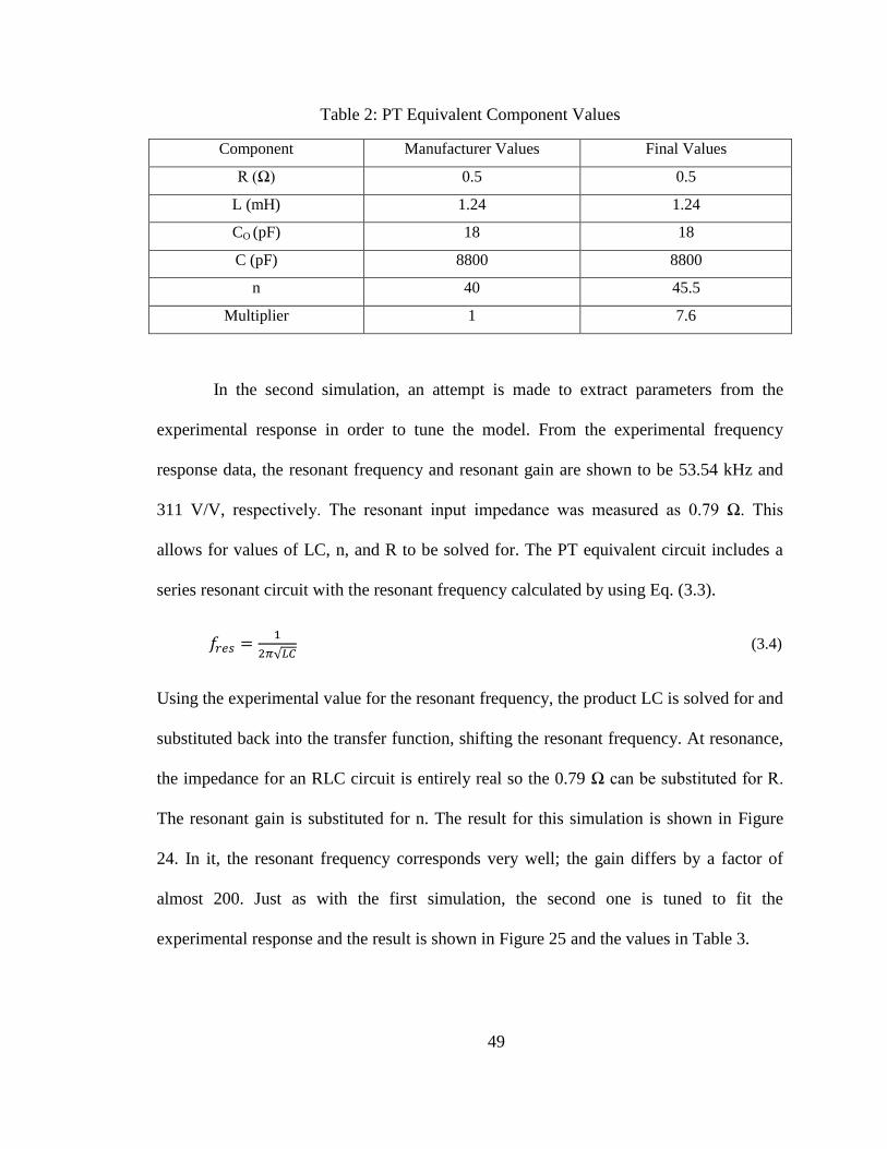
49
Table 2: PT Equivalent Component Values
Component Manufacturer Values Final Values
R (Ω) 0.5 0.5
L (mH) 1.24 1.24
CO (pF) 18 18
C (pF) 8800 8800
n 40 45.5
Multiplier 1 7.6
In the second simulation, an attempt is made to extract parameters from the
experimental response in order to tune the model. From the experimental frequency
response data, the resonant frequency and resonant gain are shown to be 53.54 kHz and
311 V/V, respectively. The resonant input impedance was measured as 0.79 Ω. This
allows for values of LC, n, and R to be solved for. The PT equivalent circuit includes a
series resonant circuit with the resonant frequency calculated by using Eq. (3.3).
(3.4)
Using the experimental value for the resonant frequency, the product LC is solved for and
substituted back into the transfer function, shifting the resonant frequency. At resonance,
the impedance for an RLC circuit is entirely real so the 0.79 Ω can be substituted for R.
The resonant gain is substituted for n. The result for this simulation is shown in Figure
24. In it, the resonant frequency corresponds very well; the gain differs by a factor of
almost 200. Just as with the first simulation, the second one is tuned to fit the
experimental response and the result is shown in Figure 25 and the values in Table 3.

50
Table 3: PT Equivalent Component Experimental Values
Component Experimental Values Final Values
R (Ω) 0.79 0.79
LC 8.83656608236E-12 8.83656608236E-12
CO (pF) 18 18
C (pF) 8800 8800
n 311 311
Multiplier 1 160
The last method used in determining equivalent component values is to employ
curve-fitting techniques. The results are shown in Figure 26.
Figure 26: Curve fitting Frequency Response
By substituting the coefficients of the PT’s transfer function with a generic a, b,
c, d, and e, a function for the curve is used and a regression is solved for using Mathcad.
45 50 55 600
100
200
300
400
Experimental
Simulated
Frequency (kHz)
Gai
n (
V/V
)

51
Mathcad uses the “genfit” command to apply a nonlinear, least-squares regression, fitted
curve.
These values can then be set equal to the coefficients in the transfer function
resulting in a nonlinear system of equations (Eqs. 3.4-3.8).
(3.4)
(3.5)
(3.6)
(3.7)
(3.8)
Their solutions result in values for equivalent components that reproduce the
experimental behavior but are not the actual characteristic equivalent parameters, since
the curve-fitting is an approximation based on a math model of the PT’s behavior within
the linear range. The equivalent values are shown in Table 4.
Table 4: PT Equivalent Component Curve-Fitting Results
Component Final Values
R (Ω) 4.4901334668E-3
L (H) -2.6603371349E-4
CO (F) -6.3540966268E-3
C (F) 2.2750052473
n 164.1903078549
Each of the three sets satisfies the approximate model of the experimental curve
and therefore each could be considered appropriate for simulation purposes. The first trial

52
illustrates just how much the actual response, under unique conditions, differs from the
manufacturer’s. The tuning parameters might be thought of as adjusting for the changes
in the equivalent component values that occur due to the approximate open-circuit
operation. The second trial offers a more intuitive approach to evaluating the equivalent
component values by extracting information from the frequency response of the PT. It
creates a response closer to the actual. The third trial relies on curve-fitting techniques for
an approximation to the actual response, from which all the equivalent component values
are calculated.
3.3 Dynamic Operation
In the second section, the PT’s behavior is simulated under dynamic conditions.
By varying n, the deviations between the physical system behavior and model
performance are observable and should illustrate where the model fails or succeeds to
synthesize an accurate response of the piezoelectric transformer under dynamic
conditions. The harsh extremes of space will subject the PT to a wide variation of
temperatures. To model this, the n parameter is adjusted and the corresponding frequency
response and input impedance is generated. This parameter, shown in the PT as the turns
ratio of the coupling transformer in the equivalent circuit, is representative of the
electrical-mechanical and mechanical-electrical energy conversion occurring within the
PT. It is a product of material properties, device geometry, and temperature. Therefore it
is the material properties, device’s dimensions, and construction that affect the PT’s gain.

53
Because the research is concerned with temperature’s effect on gain, an effort is made to
see exactly how temperature affects the device behavior. Chapter two established that the
stiffening of the piezoelectric domains causes a decrease in compliance and therefore a
rise in resonant frequency and drop in gain magnitude. Attempts to observe temperature’s
effect on dimension were inconclusive. Therefore, varying n is acceptable for some
temperature-related simulations.
Different responses for n are simulated from 45 kHz to 60 kHz and the results for
gain and input impedance are shown in Figure 27 and Figure 28, respectively.
Figure 27: PT Gain as a Function of n
45 50 55 60 650
20
40
60
n = 45
n = 40
n = 35
Voltage Gain versus n
Frequency (kHz)
Gai
n (
V/V
)

54
Figure 28: Input Impedance Magnitude as a Function of n
In the resultant simulation, as n decreases, the gain and resonant frequency
increases. Because a lowered n is a result of chilling the device, an effect that causes the
gain to decrease and resonant frequency to increase in the physical device, the model’s
response should respond similarly as well. However, as shown in Figure 27, the
simulated response does not. Figure 28 shows the effects of decreasing n on the input
impedance. Despite having not been able to acquire measurements of the input
impedance at cryogenic temperatures, results in other measurements imply what those
measurements would reveal an. First, the increase in resonant frequency shown in the
frequency response should be exactly the same in the impedance: as the temperature
drops, the resonant frequency increases. Second, in chapter two, the fact was pointed out
that as the device chills, piezoelectric domains become less mobile and this decreases
internal losses. Therefore, as the device cools, the minimum resistance should drop while
45 50 55 60 650
1
2
3
n =45
n =40
n =35
Input Impedance Magnitude versus n
Frequency (kHz)
Inp
ut
Imped
ance
Mag
nit
ud
e (S
imula
tedl)

55
the resonant frequency shifts higher. What the simulation shows instead is that with
decreasing n, the resonant frequency shifts higher (as expected) and the resonant
impedance increases. The frequency of phase shift moves higher as well.
The dynamic results behavior diverges from the expected results for cryogenic
temperatures of the PT. Experimental testing would seem to be the only way to determine
the actual response in either the frequency response or input impedance.
Based on the results from simulation of the PT’s static and dynamic behavior, it is
obvious where the model is applicable under certain conditions. In the static case, a
limited range of operation where the device is restricted to a particular operation
condition, the equivalent circuit is sufficient in reproducing the device’s response. Tuning
is necessary because even when determining the equivalent component values, the
device’s behavior is sensitive to operating conditions. For this reason, the manufacturer’s
values would not suffice and by using a curve-fitting approach, new parameters were
found that helped the model better fit the experimental results. The tuning did also
provide insight in the parameters that applied to the PT, particularly the extraction of
resonant impedance and frequency (in the form of the LC product). In all three situations,
the transfer functions were mathematically manipulated to fit the response. Results for
simulating thermal effects on the PT show the need for a higher fidelity model that
responds with more accuracy to accommodate the rigorous conditions of outer space.

56
CHAPTER IV
DRIVER CIRCUIT DESIGN
4.1 Theory of Operation and Design
The driver circuit utilizing the piezoelectric transformer consists of two parts, an
input signal source driving the PT into mechanical vibration and an output section
converting the transformers’ output AC into a DC signal usable by the ferroelectric phase
shifter.
In the input section there is a need for a high output current, high bandwidth, and
high slew rate buffer between the waveform generator and the PT. A benchtop waveform
generator (Agilent 33120A) provided the driving signal because the high quality sine
wave produced is best for efficiently and effectively driving the PT. A benchtop
waveform generator’s output frequency and magnitude can be precisely controlled which
is convenient for characterizing the device. In addition, no time was needed designing a
quality signal source just for a proof-of-concept circuit. However, the waveform

57
generator alone will not suffice and it is necessary to buffer its signal to the PT.
Integrating the buffer along with the rest of the driver circuitry is simple since it lies in
the signal path between the waveform generator and PT. In addition, adding the buffer
allows for future environmental testing of the components and is one-step closer to actual
implementation.
Texas Instruments’ OPA547T Operational Amplifier is an excellent choice for the
buffer amplifier because of its large gain-bandwidth product (GBP), high slew rate, and
large maximum output current. The GBP is 1 MHz, making it more than large enough to
span the entire bandwidth of the PTs natural resonant frequency. The Op Amp’s slew rate
is 6 V/µSec so it can drive the PT over its full dynamic range in under 10 µSec. Slewing
in amplifier’s output is very undesirable because of the harmonics it would introduce into
the PT. The driving signal amplitude need not be any greater than 9 Vpp at a peak
frequency of 54.7 kHz. With a peak continuous output current of 0.5 mA, the OPA547T
can provide constant regulation over the transformers entire dynamic range of operation.
Its negligible output offset voltage is desirable because it will not apply any DC
polarization to the PT that would otherwise oppose its AC response. Since the power of
the phase shifter controller has a 25 W budget, any energy savings is beneficial. Because
the reflectarray power consumption is a matter of scale with regard to phase shifter count,
the driver circuits are an important place to consider implementing low power
functionality. An Op Amp’s quiescent current is the current consumed by the device’s
own operation, separate from the load. This particular one has a quiescent current of only
10 mA per supply rail making it an acceptable choice for an efficient circuit. The
OPA547T also has a wide input voltage range that provides the flexibility of an even

58
wider range of operating voltages on the PT, so long as the dielectric strength of the
ceramic is not exceeded. Aside from its performance, there is also extra functionality
with the Op Amp that opens the possibility for future designs. An output enable/disable
pin and a programmable current limiting pin are included and may be used in some type
of device protection function or current feedback control strategy. The buffer circuit is a
unity gain amplifier operates in dual supply mode so that all oscillations are referenced to
ground (0 V). The current limiting feature is left disabled (by shorting to the negative
rail) enabling maximum output current. The enable/disable feature is unused as well and
disabled by shorting to the positive rail [23].
The output circuit is a voltage doubler rectifier explained in [26]. Referring to
Figure 29, Cree’s CSD01060E Schottky diodes were selected for the rectifiers.
Figure 29: Complete schematic for proof-of-concept driver circuit
Unlike PN junction diodes, Schottky diodes have no depletion region and as a
result have no reverse recovery time, negligible off-state capacitance, low forward
voltage, and near instantaneous turn off/on recovery times. Typical silicon power diodes

59
were first used but they failed to switch properly and resulted in a distorted,
underperforming output. Because the frequencies of operation are far higher than those
intended for normal rectifiers, the zero recovery time ensures that over the entire
operational range of the driver circuit, no adverse effects occur in the behavior of the PT
and the diodes function properly. Because of the potential for such high voltages on the
output, a silicon carbide component is most ideal given its extreme ruggedness. The
CSD01060E is a silicon carbide part rated for 600 Volts DC (Vdc), blocking and is used
well within its rated operation. The low off-state capacitance is only 80 pF, this means
the diode turns on and off quickly and that the equivalent junction capacitance is small
enough to effectively block the high frequency signal.
The output capacitor does not have many constraints placed upon it, so long as it
is sufficiently large enough to provide effective smoothing on the output (regulation is of
little concern as the phase shifter is over very high impedance over its entire range of
operating conditions) and is rated for the voltage on the output. The smoothing capacitor
is a 500 V, 0.01 µF part. The 500 V rating ensures dielectric breakdown will not occur
for the voltage range of operation. The time constant of the output section, the smoothing
capacitor and phase shifter (approximated as a 10 MΩ resistor), is much larger than the
switching period 1/f and therefore, the ripple on the output is negligible.
The whole circuit was laid out using Cadsoft’s EAGLE printed circuit board
design software and was chemically etched on FR-4 using UV lithography.

60
4.2 Prototype Performance Evaluation
With the driver circuit complete (shown in Figure 30), the driver’s function is
evaluated in two schemes of operation.
Figure 30: Complete Phase Shifter Driver Circuit
The first is the well familiar fixed frequency, variable input voltage drive signal.
The second was fixing the input voltage to the minimum required to reach 300 Vdc at
resonance and adjusting the drive frequency to obtain a range of voltages. In the first
approach, the input frequency was set to the resonant frequency determined when the PT
was out of the cryostat (54 kHz). The results are shown in Figure 31.

61
Figure 31: Driver Circuit Voltage Output For Fixed Fin and Variable Vin
From the response it is clear the circuit exhibits hysteresis and that a memory is
present in the device. This behavior complicates phase shifter performance.
The second scheme’s results are shown in Figure 32 and they show no memory
effects.
0
50
100
150
200
250
300
350
400
0 2 4 6 8 10 12
Ou
tpu
t V
olt
ag
e (V
DC
)
Input Voltage (Vpp)
Driver Circuit Voltage Output for Fixed fin and Variable Vin
Variable Vin (Ascending)
Variable Vin (Descending)

62
Figure 32: Driver Circuit Voltage Output for Fixed Vin and Variable Fin
So, although both are able to reach the full dynamic range required for the phase
shifter’s correct operation, the variable frequency scheme proves the more effective due
to the absence of hysteresis. From Figure 32, the range of frequencies over which the
driver switches in order to sweep the whole range of voltages is narrow, and because
there is no hysteresis, the control effort in any future controller setup is simplified.
0
50
100
150
200
250
300
350
400
45 50 55 60
Ou
tpu
t V
olt
ag
e (V
DC
)
Input Frequency (kHz)
Driver Circuit Voltage Output for Fixed Vin and Variable fin
Variable fin (Ascending)
Variable fin (Descending)

63
4.3 Integration with the Ferroelectric Phase Shifter
Now with the driver circuit evaluated, the phase shifter is connected and the
whole circuit’s performance is determined. Leads, connected to the bias tees, are wired
directly to the output of the rectifier. From the driver circuit’s point of view, there should
be little difference between the high impedance probe and the phase shifter, so the
behavior should be the same. The phase shifter was driven using both the fixed frequency
and fixed voltage methods. The phase shift is measured at 27.5 GHz using an Agilent
E8561A vector network analyzer. The frequency was adjusted so that the output voltage
reached the desired level. Starting with Figure 33, a drive frequency of 42.79 kHz,
produced 0.1 Vdc on the output and 139.21 degrees on the phase shifter. This is
essentially the ground state for the phase shifter and represents a relative phase shift of
zero. It includes insertion phase not capable of being de-embedded because of differences
between the calibration plane and the measurement plane. At 46.01 kHz the voltage is 1
Vdc and 139.39 degrees phase shift result, shown in Figure 34. Figure 35 is the result of
50.48 kHz, which generates 10 Vdc and results in 144.98 degrees phase shift. Shown in
Figure 36, with 52.21 kHz, 50 Vdc is generated and 165.71degrees result. In Figure 37, a
drive frequency of 52.82 kHz, produced 100 Vdc on the output and -179.24 degrees on
the phase shifter. At 53.46 kHz, the voltage is 300 Vdc and -123.1 degrees phase shift
result, shown in Figure 38.

64
Figure 33: Fin = 42.79 kHz, 0.1 Vdc Applied, 139.21 Degrees Phase Shift Result
Figure 34: Fin = 46.01 kHz, 1.0 Vdc Applied, 139.39 Degrees Phase Shift Result

65
Figure 35: Fin = 50.48 kHz, 10.0 Vdc Applied, 144.98 Degrees Phase Shift Result
Figure 36: Fin = 52.21 kHz, 50.0 Vdc Applied, 165.71 Degrees Phase Shift Result

66
Figure 37: Fin = 52.82 kHz, 100.0 Vdc Applied, -179.24 Degrees Phase Shift Result
Figure 38: Fin = 53.46 kHz, 300.0 Vdc Applied, -123.10 Degrees Phase Shift Result
Preliminary results were successful with the driver achieving an output voltage
from 0 to 300 Vdc and accomplishing about 98 degrees of phase shift (+139 to -123).
Results were limited to less than a full 2π, but this is due to the phase shifter’s design and
not the driver circuit.

67
CHAPTER V
CONCLUSION
5.1 Summary
This research successfully demonstrates the implementation of a piezoelectric
transformer in a ferroelectric phase shifter driver circuit. A proof-of-concept driver
circuit, based on the PT, outputs voltages in excess of 400 Vdc from an input ranging
from 1 to 10 Vac. This causes the phase shifter to insert up to 180 degrees of phase shift
at Ka-band.
Research started with a literature review, where the fundamentals of piezoelectric
and ferroelectric materials were investigated. This knowledge compliments further
readings about piezoelectric transformers. Important to this work was other research
studying the device’s behavior and its applications. The next section discusses the need to
characterize the piezoelectric transformer over temperature. Because the PT is nonlinear,
particularly in response to its temperature, it is necessary to determine the frequency
response and input impedance. Experiments were designed to measure the gain versus

68
frequency at room and cryogenic temperatures and the input impedance versus frequency
at room and cryogenic temperatures as well. An attempt was also made at measuring the
device’s physical response to cryogenic temperature by using a laser radar; without any
conclusive results, unfortunately. Chapter two explored the equivalent circuit in greater
detail and its applications. The theoretical response from the model is compared to the
experimental response. By taking into consideration the nonlinearities that are present in
the physical system that are not present in the model, an attempt is made at reconciling
the two. This leads to the next step of extracting new equivalent circuit values that will
generate the same response for the piezoelectric transformer’s particular point of
operation in the experimental operation phase. In section three, the design, theory of
operation, and evaluation of a proof-of-concept driver circuit for the ferroelectric phase
shifter is presented. Based partly on a well-established doubler-rectifier design and using
the data gathered in the previous section, a driver circuit was laid out. Test points were
included in the design to allow for measurements as well as interfacing with the phase
shifter itself. Two modes of operation for the driver circuit were realized: one where the
input signal’s frequency was kept fixed at resonance and the magnitude varied, and the
other where the magnitude was kept fixed and the frequency adjusted. The presence of
hysteresis in the driver circuit’s output when operating in the fixed frequency mode
makes the fixed input voltage mode preferable. Efficiency data in the form of current
drawn by the PT’s driver circuit was measured as well. In chapter four, the phase shifter
was integrated with the driver circuit and functionality is tested by measuring the change
in phase shift as the circuit applies different voltages.

69
This work was presented as an invited talk on August 3, 2011 at the 2011
International Symposium on Integrated Functionalities in Cambridge, England. It will be
published in a 2012 edition of Integrated Ferroelectrics (Volume 134, Issue 1).
5.2 Future Research and Work
This research, apart from developing a low power, lightweight and high-
performance driver circuit using a piezoelectric transformer, furnishes the novel design
concept of marrying ferroelectrics and piezoelectrics within a single application, a pairing
that can evolve into many more applications. Also novel in this work are the cryogenic
characterization of a piezoelectric transformer and the evaluation of multiple modes of
operation, namely the fixed frequency-variable voltage and fixed voltage-variable
frequency modes. The cryogenic exposure mimicked the effects that the PT would
encounter in the cold of space. The two driving modes revealed how the PT functions in
operation and how the hysteresis manifests itself in the device. Through this work, a
unique and new alternative to magnetic components in ferroelectric phase shifter drivers
is offered.
With the completion of the driver circuit, the issue of future work arises. Areas
that warrant future pursuits are the characterization of the piezoelectric transformer,
further development of the driver circuit, and the implementation of the driver circuit
with the ferroelectric reflectarray antenna.

70
By better characterizing the PT, a greater understanding of its behavior is
established. This knowledge could help in the improvement of the driver circuit design.
Using precision thermo-mechanical data, a greater insight to the device’s frequency
response at cryogenic temperatures is established. This information might be useful in
creating improved computer models of the device or when selecting piezoelectric
transformers for similar applications. However, because the laser radar failed to scan the
PT with the precision required for an accurate dimension reading, an alternative might be
to use a microscope with an eyepiece micrometer.
Modeling is a powerful tool for engineering analysis and design. As discussed in
chapter three, the equivalent circuit model for the PT is limited to a narrow, linear range
of operation. Further complicating modeling efforts is the presence of a split-resonance at
cryogenic conditions, a non-linear situation. This suggests a model is two, coupled,
resonant circuits. It is this coupling that is either dampened or exacerbated by the effects
of temperature. Future research of dual resonance in piezoelectric transformers should
investigate the following: its cause, whether or not it is common in all types of PTs, and
if it can be accurately modeled. Appendix A provides a preliminary attempt at modeling
the dual-resonance encountered experimentally. The peculiar impedance of the device
provides insight into an improved model. What it suggests is a series resonance followed
by a parallel one. Ascertaining the causes of this behavior and how to model it provide
invaluable information on the PT’s functionalities. By taking advantage of the device’s
behavior, better driving circuitry (perhaps for improved efficiency or performance) can
be developed. An improved model offers the parameters for better controller design. It

71
also leads to improved output circuitry, making the device available for broader
applications or improving its performance.
Now that it has been shown the piezoelectric transformer can bias a ferroelectric
phase shifter, further work lies in maturing this technology. One place to start is device
control and driving. Chapter two made the point that the device is very nonlinear over
temperature and frequency therefore, in order to be sure the phase shifter is outputting the
required voltage, regardless of temperature, some type of control scheme is necessary.
Whether this controller is integrated with the phase shifter or off board, is left to future
design but it will have to compensate for the change in resonant frequency and gain by
adjusting the driving frequency and amplitude. This might be accomplished via a
feedback loop where the output voltage is compared to a set point and using either
temperature measurements, input current readings, or both, the drive signal is adjusted.
The rectifier circuitry might also be another place for improvement. The rectifier-doubler
was only chosen because it was an established, effective means to supply high voltage
DC to a high impedance load. It may be, however, that a better topology could be
realized that affects PT behavior in some unforeseen, positive way. The driving signal,
currently supplied by the waveform generator and buffered by an Op Amp, might be
practically implemented in a number of ways. A signal bus could supply entire groups of
drivers and therefore be located away from the PTs. Alternatively; a signal source might
be integrated with the PT and have only control signals routed to it. If the driver could
eliminate the buffer circuit while providing the source current and signal properties,
energy and cost savings could be realized. Future research might also reveal interesting
options in the driving signal. Despite current understanding that a single tone is the

72
preferred way to drive the device, perhaps there may be use in driving the PT with a
polytone signal. An example of such a use is a control scheme that derives the PT’s
operating information by comparing two or more signals injected into the PT. Another
use is using a polytone signal as a way to boost the output voltage. Despite being a niche
technology, a few companies do offer a selection of piezoelectric transformers with
variations based on poling, construction, and piezoelectric properties. Among the PT
product lines, there may be a device better suited to this research’s purpose than the
SMMTF53P2S40. Perhaps there is a PT with higher input impedance and therefore a
smaller Q and lesser current draw, or one that is not as affected by temperature.
Once the driver circuit reaches the necessary level of functionality, it can be
integrated with the phase shifter. A way must be found to attach the drivers to the
backplane of the reflectarray, as this configuration is optimal for performance and
packaging reasons. An approach must also be found to address each driver circuit and to
maintain the phase shifter’s performance. The driver circuit will also have to be evaluated
for space and flight worthiness, which may necessitate a redesign that includes the
substitution of radiation-hardened components.
By successfully demonstrating how a driver circuit based on piezoelectric
transformer technology can bias a ferroelectric phase shifter, the groundwork is laid for a
myriad of applications in analog and power electronics.

73
REFERENCES
1. Robert Romanofsky and A.H. Qureshi, "A Model for Ferroelectric Phase Shifters,"
IEEE Transactions On Magnetics, vol. 36, no. 5, pp. 3491-3494, September 2000.
2. Robert R Romanofsky, "Advances in Scanning Reflectarray Antennas Based on
Ferroelectric Thin Film Phase Shifters for Deep Space Communications," NASA,
Cleveland, Technical Memorandum 214983, 2007.
3. Bernard Jaffe, "A Primer on Piezoelectricity and Piezoelectric Ceramics," Morgan
Electro Ceramics, Technical Publication TP217,. [Online]. www.morgan-
electroceramics.com
4. Robert R Romanofsky, "Array Phase Shifters: Theory and Technology," NASA,
Cleveland, Technical Memorandum 214906, 2007.
5. Donald Priebe, "Reflectarray Controller Operations & ICD Document," ZIN
Technologies, Inc., Brookpark, AST-OPS-103, 2003.
6. Morgan Electro Ceramics, "Piezoelectricity," TP-238,. [Online]. www.morgan-
electroceramics.com
7. James R Phillips, "Piezoelectric Technology Primer," CTS Wireless, Albuquerque,
NM, May 2000. [Online].
http://www.ctscorp.com/chn/components/pzt/downloads/Piezoelectric_Technology.
8. APC International, Ltd., Piezoelectric Ceramics: Principles and Applications.: APC
International, Ltd., 2002.
9. Murata Manufacturing Co., "Piezoelectric Ceramics (PIEZOTITE) Sensors,"
Catalougue No. P19E-9. [Online]. www.murata.com
10. E.L. Horsley, M.P. Foster, and D.A. Stone, "State-of-the-art Piezoelectric
Transformer Technology," in European Conference on Power Electronics and
Applications, Aalborg, DK, 2007, pp. 1-10.
11. Gregory Ivensky, Isaac Zafrany, and Shmuel Ben-Yaakov, "Generic Operational
Characteristics of PIezoelectric Transformers," IEEE Transactions on Power
Electronics, vol. 17, no. 6, pp. 1049-1057, November 2002.
12. I Kartashev, T Vontz, and H Florian, "Regimes of piezoelectric transformer
operation," Measurement Science and Technology, vol. 17, no. 8, pp. 2150-2158,
July 2006.
13. Steiner & Martins Inc. (2011, February) RE: "Thick" PT Input Capacitances. Email.
14. Steiner & Martins, Inc. (2010, October) Multilayer piezoelectric transformer
material - 1931. Email.

74
15. Steiner & Martins, Inc. (2010, October) RE: Multilayer piezoelectric transformer
material - 1931. Email.
16. Hyun-Woo Joo, Chang-Hwan Lee, Jong-Seok Rho, and Hyun-Kyo Jung, "Analysis
of Temperature Rise for Piezoelectric Transformer Using Finite-Element Method,"
IEEE Transactions on Ultrasonics, Ferroelectrics, and Frequency Control, vol. 53,
no. 8, pp. 1449-1457, August 2006.
17. Morgan Electro Ceramics, "Piezoelectric and dielectric properties of Lead Titanate
Zirconate at low temperatures," Technical Publication TP-224,. [Online].
www.morgan-electroceramics.com
18. Matthew W Hooker, "Properties of PZT-Based piezoelectric Ceramics between -150
and 250 C," Lockheed Martin Engineering & Sciences Co., Hampton, VA, NASA
Contractor Report 208708, 1998.
19. Kuo-Tsai Chang, "Effects of Load Resistance on Step-Up Voltage Gains of Rosen-
Type Piezoelectric Transformer," in IEEE International Conference on Industrial
Technology, Hong Kong, Hong Kong, 2005, pp. 1080 - 1085.
20. E.L. Horsley, M.P. Foster, and D.A. Stone, "A frequency-response-based
characterisation methodology for piezoelectric transformers," in 2nd Electronics
System-Integration Technology Conference, Greenwich, UK, 2008, pp. 959-962.
21. Morgan Electro Ceramics Inc. (2007, November) Morgan Electro Ceramics Inc.
[Online]. http://www.morganelectroceramics.com/resources/literature/
22. Steiner & Martins Inc. (2010, October) Multilayer piezoelectric transformer material
- 1931. Email.
23. Texas Instruments Inc. (2005, July) Texas Instruments Inc. [Online].
http://www.ti.com/product/opa547
24. D.A. Berlincourt, "General Description of Piezoelectric Transformers," Morgan
Electro Ceramics , Technical Publication TP-244, 1999.
25. I Kartashev and T Vontz, "Regimes of piezoelectric transformer operation II,"
Measurement Science and Technology, vol. 20, no. 5, pp. 1-14, April 2009.
26. Gregory Ivensky, Moshe Shvartsas, and Shmuel Ben-Yaakov, "Analysis and
Modeling of a Voltage Doubler Rectifier Fed by a Piezoelectric Transformer," IEEE
Transactions on Power Electronics, vol. 19, no. 2, pp. 542-549, March 2004.
27. Jesús Manuel González-Miranda, Synchronization And Control Of Chaos: An
Introduction For Scientists And Engineers.: Imperial College Press, 2004.

75
APPENDIX
The appendix addresses continued work in developing a model of the double
resonant behavior of the piezoelectric transformer. Although beyond the scope of this
work, the PT’s double resonance bears mentioning because of the strong semblance that
the results in [27] have to those in chapter two and the profound effect this effect could
have on device operation that might limit its applications to space technology. So with
further effort, it may be possible to build off of the aforementioned work and use it in
investigating a potential model for the double resonant behavior for the purposes of
understanding the device better, aiding in the development of electronics, and controlling
the device.
The double resonance began appearing in the extreme cryogenic temperatures
used in chapter two. It was postulated that the extreme cold affected the mechanical
coupling between each half of the device, causing them to resonate independently of each
other rather than as one whole piece. In [27], the author devotes a chapter to analyzing
coupled and driven harmonic oscillators by using two coupled mass-spring-damper
mechanical systems as a model (Figure 39).
Figure 39: Coupled Mass-Spring-Damper System

76
Analyzing the author’s model yields the equations of motion for the above system
and they are given in (A.1) and (A.2).
(A.1)
(A.2)
Here F1 is the applied force to block m1, and B1 and B2 are the friction
coefficients for blocks one and two, respectively. The author manipulates the equations to
their form in (A.3) and (A.4) and provides a general solution in equations (A.5) and
(A.6), respectively.
(A.3)
(A.4)
(A.5)
(A.6)
For an initial application, the above model is manipulated to match the frequency
response for the piezoelectric transformer. To do so, the experimental values for each
resonant peak in the experimental response (Figure 1) are substituted in Equation (A.6)
and evaluated using Mathcad. A1 and A2 are the peak amplitudes and are set equal to one;
δ1 and δ2 are the relative phase shifts and are set equal to zero. For the resonant
frequencies, ω2 is related to ω1 by the equation , where κ is the coupling
coefficient [27]. By assigning the first of the split resonance values to (54.9 kHz), κ can

77
then be varied (8650) until matches the experimental value (56.3 kHz). The time
domain response is shown in Figure 40 and the frequency response is shown in Figure 41.
All results are computed using Mathcad.
Figure 40: PT Dual-Resonance Time Domain Response
Figure 41: PT Dual-Resonance Frequency Domain Response

78
What results are very clearly the split resonant peaks of the cryogenically
operating piezoelectric transformer. This shape can be compared with the experimental
response of Figure 17.
Based off of these results, future work could investigate relating the equations’
parameters to those of the actual piezoelectric transformer, further investigating the
theory of the device’s operation and developing an improved model of the coupling and
performance of the PT at cryogenic temperatures.
The author’s work [27] can be extended into the electrical domain, yielding a
circuit that is familiar from earlier sections of this work. An equivalent analog of the
mechanical systems can be written by replacing linear displacement (x) with charge (q),
allowing an equivalent electrical circuit to model the same system. From equations (A.1)
and (A.2), the equivalent electrical equations are given below.
(A.7)
(A.8)
What results are a set of loop equations that describe the equivalent circuit shown
in Figure 42.
Figure 42: Equivalent Electrical Circuit

79
This is not unlike the coupled piezoelectrics present in the PT and therefore may
make a good template for the cryogenic model of the device.
Such a circuit might aid future work in the design of future electronics based on
the PT operating at cryogenic temperatures