Embed Size (px)
Citation preview

Implementation of FPGA in the design of
Embedded Systems
1. Prioritized Highway Traffic Light Controller
2. Speech Encryption / Decryption
A THESIS SUBMITTED IN PARTIAL FULFILMENT
OF THE REQUIREMENTS FOR THE DEGREE OF
Bachelor of Technology
In
Electronics and Communication Engineering
By
K. Srinivas
Roll No: 10407035D
&
Srikanth P.K.A.S
Roll No: 10307015
Department of Electronics and Communication Engineering
National Institute of Technology, Rourkela
May, 2007

Implementation of FPGA in the design of
Embedded Systems
1. Prioritized Highway Traffic Light Controller
2. Speech Encryption / Decryption
A THESIS SUBMITTED IN PARTIAL FULFILMENT
OF THE REQUIREMENTS FOR THE DEGREE OF
Bachelor of Technology
In
Electronics and Communication Engineering
By
K. Srinivas
Roll No: 10407035D
&
Srikanth P.K.A.S
Roll No: 10307015
Under the guidance of
Prof. K.K. Mahapatra
Department of Electronics and Communication Engineering
National Institute of Technology, Rourkela
May, 2007

National Institute of Technology
Rourkela
CERTIFICATE
This is to certify that the thesis entitled, “Implementation of FPGA in the design of
Embedded Systems” submitted by K. Srinivas in partial fulfillment of the requirements for
the award of Bachelor of Technology Degree in Electronics and communication Engineering
at the National Institute of Technology, Rourkela (Deemed University) is an authentic work
carried out by him under my supervision and guidance.
To the best of my knowledge, the matter embodied in the thesis has not been submitted to any
other university / institute for the award of any Degree or Diploma.
Date: Prof. K. K. Mahapatra
Dept. of Electronics & Comm. Engineering
National Institute of Technology, Rourkela
Pin - 769008

National Institute of Technology
Rourkela
ACKNOWLEDGEMENT
I am thankful to Dr. K. K. Mahapatra, Professor in the department of Electronics and
Communication Engineering, NIT Rourkela for giving me the opportunity to work under him
and lending every support at every stage of this project work.
I would also like to convey my sincerest gratitude and indebt ness to all other faculty
members and staff of Department of Computer Science and Engineering, NIT Rourkela, who
bestowed their great effort and guidance at appropriate times without which it would have
been very difficult on my part to finish the project work.
Date K. Srinivas
Dept. of Electronics & Comm. Engineering
National Institute of Technology, Rourkela
Pin - 769008

CONTENTS
A. ABSTARCT iii B. List of Figures v C. List of Tables vi D. CHAPTERS
1 INTRODUCTION
2 FPGA AND ITS DESIGN FLOW
2.1 Fundamentals of FPGA
2.2 Design flow
2.3 VHDL
3 DESIGN NO-1
HIGHWAY TRAFFIC LIGHT CONTROLLER
3.1 Introduction
3.2 Literature review
3.3 Protocol
4 TLC IMPLEMENTATION USING LOGIC GATES
4.1 Hardware design
4.2 Finite State Machine
4.3 Karnaugh Map
4.4 Hardware implementation
5 OVERVIEW OF SPARTAN-2
6 TRAFFIC LIGHT EMBEDDED SYSTEM
6.1 Block Diagram
6.2 Design Problems
7 RESULTS OF TLC
7.1 Test bench for clock divider
7.2 Test bench for different input signals
8 DESIGN-2
SPEECH ENCRYPTION AND DECRYPTION
8.1Introduction

9 FUNDAMENTALS OF ENCRYPTION AND DECRYPTION
9.1 Introduction
9.2 Types of cipher
9.3 Data encryption standard
10 OVERVIEW OF VIRTEX II PRO
11 DEVELOPMENT OF ENCRYPTING AND DECRYPTING SYSTEM
11.1 Offline process
11.2 Online Process
11.3 Discussion
12 CONCLUSIONS
E. REFERENCES

Abstract
The use of FPGAs (Field Programmable Gate Arrays) and configurable processors is
an interesting new phenomenon in embedded development. FPGAs offer all of the features
needed to implement most complex designs. Clock management is facilitated by on-chip PLL
(phase-locked loop) or DLL (delay-locked loop) circuitry. Dedicated memory blocks can be
configured as basic single-port RAMs, ROMs, FIFOs, or CAMs. Data processing, as
embodied in the devices’ logic fabric, varies widely. The ability to link the FPGA with
backplanes, high-speed buses, and memories is afforded by support for various single ended
and differential I/O standards. Also found on today’s FPGAs are system-building resources
such as high speed serial I/Os, arithmetic modules, embedded processors, and large amounts
of memory.
Here in our project we have tried to implement such powerful FPGAs in the design of
possible embedded systems that can be designed, burned and deployed at the site of operation
for handling of many kinds of applications. In our project we have basically dealt with two of
such applications –one the prioritized traffic light controller and other a speech encrypting
and decrypting system.
Our first design is the traffic light controller which implements Finite State Machines
and timers on FPGA. Optimal traffic signal settings at a signalized intersection can minimize
the vehicle delay time, stops, and queue length at a stop line. The controller is to be designed
to control the traffic lights of a busy highway (HWY) intersecting a side road (SRD) that has
relatively lighter traffic load. The heart of the system is a finite state machine (FSM) that
directs the unit to light the main and side street lights at appropriate times for the specified
time intervals. Here FSM is designed such that it gives priority to Highway road than side
roads. Also FSM is designed such that it will give priority to emergency (Ambulance)
vehicles on either side of the road. For this FSM takes input from sensors placed on the
highway road and side road. After finalizing we have written VHDL module FSM design.
Finally algorithm is designed, simulated, implemented on a FPGA and then hardware is
tested. Here we have chosen Spartan-2 platform FPGA for implementing Traffic light
control.

Our second example is Digital Encryption or Decryption of Speech which
implements complex algorithm of FPGA. Digital Encryption of Speech signal is the most
powerful protection technique against eves dropping and wire taping of telephone
communication lines. In this project we implemented Symmetric-Key Cryptography system.
In symmetric-key cryptography, a common key is shared by both sender and receiver. The
sender uses an encryption algorithm and the same key space to encryption of data and the
receiver uses a decryption algorithm and the same key space for the decryption of data. Here
Stream Cipher of Data Encryption Standard algorithm is used. Stream cipher is a class of
ciphers in which encryption or decryption is done using separate keys which are generated
using some key generating function. In our context the key space consists of 30 different keys
for a 30 data sample and the key space repeats itself for the subsequent data samples. Also a
shift algorithm is used to obtain these 30 different keys. Algorithm consists of generation of
key space and X-ORing of this key space with 30 data samples is designed, simulated,
implemented on an FPGA and finally the hardware is tested. The encryption or decryption
algorithm is designed all in VHDL. The design also contains Analog to Digital converter and
Digital to Analog converter stand alone chips to handle speech signals in the transmitter and
receiver sides along with audio filters and amplifiers. So we have selected Virtex II Pro
platform FPGA for implementing our speech encryption algorithm. The transmitter and
receiver parts of the system are connected directly together in back to back mode. The final
design is downloaded on Virtex II Pro device and hardware tested.

List of Figures
Fig. 2.1 Design Flow for FPGA
Fig. 2.2 Final Gate Level Simulation Stages
Fig 3.1 Crossover Between Side Road(SRD) and Highway(HWY)
Fig 4.1 Sequential Circuit Design
Fig 4.2 Finite State Machine
Fig 4.3 Sequential Circuit For FSM
Fig 4.4 Implementation on Bread Board
Fig 4.5 Logic Circuit for Dx
Fig 4.6 Logic Circuit for Dy
Fig 4.7 Logic Circuit for Dz
Fig 4.8 Logic Circuit for Combinational Design
Fig 5.1 Floor plan of Spartan 2
Fig 6.1 Block Diagram of TLC
Fig 7.1 Test-Bench for Clock Divider
Fig 7.2 Test-Bench for four bit Clock divider
Fig 7.3 Test-Bench Waveform when SH=0, SG=0
Fig 7.4 Test-Bench Waveform when there is an exception in SG=1, SH=0 during divided
clock period
Fig 7.5 Test-Bench Waveform when there is an exception in SG=1, SH=0 during divided
clock period
Fig 9.1 Block Diagram for Standard Encryption and Decryption
Fig 9.2 Following figure shows the idea about encryption and decryption of messages
Fig 9.3 Symmetric –Key Cryptography System
Fig 9.4 A Model of DES
Fig 9.5 ECB Mode of DES
Fig 9.6 CBC Mode OF DES
Fig 9.7 CFM Mode of DES
Fig 9.8 CSM Mode of DES
Fig 11.1 Offline Process
Fig 11.2 Online Process
Fig 11.3 Symmetric-Key Cryptography System

List of Tables Table No. 4.1 Truth-Table for Combinational Circuit Design
Table No. 4.2 Truth-Table for Sequential Circuit Design

Chapter 1
INTRODUCTION

The latest technologies being developed now-a-days primarily aim towards
automation in real-time. Some of the illustrative examples are NASA’s Mars rovers, Robots,
Mobile Cellular phones, DVD players, etc. Each of these applications performs a specific
defined function. Such systems, which pave way for automation, are based on the basic
concept called “REAL-TIME EMBEDDED SYSTEM”.
Introduction - Real-Time Embedded Systems
REAL-TIME SYSTEMS: - Timeliness is the single most important aspect of a real-
time system. These systems respond to a series of external inputs, which arrive in an
unpredictable fashion. The real-time systems process these inputs, take appropriate decisions
and also generate output necessary to control the peripherals connected to them. “A real-time
system is one in which the correctness of the computations not only depends upon the logical
correctness of the computation but also upon the time in which the result is produced. If the
timing constraints are not met, system failure is said to have occurred”.
It is essential that the timing constraints of the system are guaranteed to be met.
Guaranteeing timing behavior requires that the system be predictable. The design of a real-
time system must specify the timing requirements of the system and ensure that the system
performance is both correct and timely. There are three types of time constraints:
� HARD: A late response is incorrect and implies a system failure. An example of such a
system is of medical equipment monitoring vital functions of a human body, where a late
response would be considered as a failure.
� SOFT: Timeliness requirements are defined by using an average response time. If a single
computation is late, it is not usually significant, although repeated late computation can
result in system failures. An example of such a system includes airlines reservation
systems.
� FIRM: This is a combination of both hard and soft timeliness requirements. The
computation has a shorter soft requirement and a longer hard requirement. For example, a
patient ventilator must mechanically ventilate the patient a certain amount in a given time
period. A few seconds’ delay in the initiation of breath is allowed, but not more than that.
One needs to distinguish between on-line systems such as an airline reservation system,
which operates in real-time but with much less severe timeliness constraints than, say, a
missile control system or a telephone switch. An interactive system with better response time

is not a real-time system. These types of systems are often referred to as soft real time
systems. In a soft real-time system (such as the airline reservation system) late data is still
good data. However, for hard real-time systems, late data is bad data.
Most real-time systems interface with and control hardware directly. The software for
such systems is mostly custom-developed. Real-time Applications can be either embedded
applications or non-embedded (desktop) applications. Real-time systems often do not have
standard peripherals associated with a desktop computer, namely the keyboard, mouse or
conventional display monitors.
EMBEDDED SYSTEMS
An embedded system is a combination of computer hardware, software and electro-
mechanical parts tailored for a dedicated single or combinations of functions. The end user
cannot program it. A user can make choices concerning functionality but cannot change the
functionality of the system by adding / replacing software. Embedded systems do not provide
standard computing services and normally exist as part of a bigger system. A computerized
washing machine is an example of an embedded system where the main system provides a
non-computing feature (washing clothes) with the help of an embedded computer. Embedded
systems are usually constructed with the least powerful computers that can meet the
functional and performance requirements. This is essential to lower the manufacturing cost of
the equipment.
With an embedded system, the hardware can be identified but the software that really
supplies the system’s functionality can be hidden and more difficult to analysis. The software
is already burnt into the on-chip memory and is effectively impossible to access. Other
components of the embedded system are similarly chosen, so as to lower the manufacturing
cost.
Some systems are mission critical systems which are hard real-time systems whose
failure can cause catastrophic results. The best way to deal with this situation is the use of
Real-time Embedded systems. In most of the real-life applications, real-time systems often
work in an embedded scenario and most of the embedded systems have real-time processing
needs. Such software is called Real-time Embedded Software systems.
In our project we went for the design of such kind of embedded systems by using an
FPGA as our main processing block and implementing the characteristic features of an FPGA
in the development of single purpose specifically designed embedded platforms.

Chapter 2
FPGA AND ITS DESIGN FLOW

Fundamentals of FPGA
The use of FPGAs (Field Programmable Gate Arrays) and configurable processors is
an interesting new phenomenon in embedded development. The last few years have seen a
dramatic increase in the use of FPGAs as an early prototyping environment for a traditional
ASIC (Application Specific Integrated Circuit). The flexibility of an FPGA benefits the
design lifecycle, bringing savings in time and effort in the prototyping stage and in the
integration of software and hardware in the design phase. In some cases, the development
team is choosing to replace the ASIC altogether in the final design with the FPGA making it
into a shipping product. These decisions are causing a shift in the embedded software
landscape, which is being driven by the new choices in processors.
The use of FPGAs is growing in embedded designs and the embedded systems
software market must continue to change to support this shift. With the added flexibility of
the FPGA-based design, the embedded software solution, specifically the RTOS (Real Time
Operating System), middleware, and drivers should complement the benefits of the FPGA.
The RTOS should be well designed and easy-to-use, with the necessary and sufficient
offering of middleware stacks and drivers. In addition to this prerequisite, the RTOS should
also maintain the characteristics related to embedded designs, namely small code size, low
interrupt latency, and full services needed for your application. The use of an FPGA is a
growing trend. Because of the flexibility of the FPGA, it is applicable in a wide range of
markets.
FPGAs are being forecasted for use in several industries, from consumer electronics
to military/aerospace, automotive to industrial control. The trade-offs between using an
FPGA and an ASIC can create a difficult decision with development teams. The FPGA
provides developers with much more flexibility in the ability to customize the part
specifically for their application. However, the lower costs associated with an ASIC provide
for a sound argument when viewed from a business case. In several cases, the issue can be
confounded with the use of embedded cores within an FPGA. Several vendors offer FPGAs
to the market, with two of the largest, Xilinx and Altera, offering embedded cores and
configurable cores. Together, companies offer a wide range of choices to developers for use
in their FPGA-based designs.

FPGA Design Flow:
Design Entry:
The process of implementing a design on an FPGA can be broken down into several
stages, loosely definable as design entry or capture, synthesis, and place and route. For many
designers, the choice of whether to use schematic- or HDL-based design entry comes down to
their conception of their design. For those who think in software or algorithmic-like terms,
HDLs are the better choice. HDLs are well suited for highly complex designs, especially
when the designer has a good handle on how the logic must be structured. They can also be
very useful for designing smaller functions when you haven’t the time or inclination to work
through the actual hardware implementation.
Fig. 2.1 Design Flow for FPGA
RTL Simulation:
After design entry, the design is simulated at the register-transfer level (RTL). This is
the first of several simulation stages, because the design must be simulated at successive
levels of abstraction as it moves down the chain toward physical implementation on the
FPGA itself. RTL simulation offers the highest performance in terms of speed.

The next step following RTL simulation is to convert the RTL representation of the
design into a bit-stream file that can be loaded onto the FPGA. The interim step is FPGA
synthesis, which translates the VHDL or Verilog code into a device netlist format that can be
understood by a bit-stream converter.
Synthesis Process:
The synthesis process can be broken down into three steps. First, the HDL code is
converted into device netlist format. Then the resulting file is converted into a hexadecimal
bit-stream file, or .bit file. This step is necessary to change the list of required devices and
interconnects into hexadecimal bits to download to the FPGA. Lastly, the .bit file is
downloaded to the physical FPGA. This final step completes the FPGA synthesis procedure
by programming the design onto the physical FPGA.
Gate Level Simulation Process:
Functional simulation is performed after synthesis and before physical
implementation. This step ensures correct logic functionality. After implementation, there’s a
final verification step with full timing information. After placement and routing, the logic and
routing delays are back-annotated to the gate-level netlist for this final simulation. At this
point, simulation is a much longer process, because timing is also a factor. Often, designers
substitute static timing analysis for timing simulation. Static timing analysis calculates the
timing of combinational paths between registers and compares it against the designer’s timing
constraints. At the completion of placement and routing, a binary programming file is
created. It’s used to configure the device.
Fig. 2.2 Final Gate Level Simulation Stages

FPGAs must be programmed by users to connect the chip’s resources in the
appropriate manner to implement the desired functionality. Over the years, various
technologies have emerged to suit different requirements. Some FPGAs can only be
programmed once. These devices employ antifuse technology. Flash-based devices can be
programmed and reprogrammed again after debugging. Still others can be dynamically
programmed thanks to SRAM-based technology. Each has its advantages and disadvantages.
Most modern FPGAs are based on SRAM configuration cells, which offer the benefit
of unlimited reprogram ability. When powered up, they can be configured to perform a given
task, such as a board or system test, and then reprogrammed to perform their main task. On
the flip side, though, SRAM-based FPGAs must be reconfigured each time their host system
is powered up, and additional external circuitry is required to do so. Further, because the
configuration file used to program the FPGA is stored in external memory, security issues
concerning intellectual property emerge.
As the number of enhancements to various Hardware Description Languages (HDLs)
has increased over the past year, so too has the complexity of determining which language is
best for a particular design. Many designers and organizations are contemplating whether
they should switch from one HDL to another. Each HDL has its own style and heredity. The
following descriptions provide an overall “feel” for each language. A table at the end of the
paper provides a more detailed, feature-by-feature comparison.
VHDL
VHDL is a strongly and richly typed language. Derived from the Ada programming
language, its language requirements make it more verbose than Verilog. The additional
verbosity is intended to make designs self-documenting. Also, the strong typing requires
additional coding to explicitly convert from one data type to another (integer to bit-vector, for
example). The creators of VHDL emphasized semantics that were unambiguous and designs
that were easily portable from one tool to the next. Hence, race conditions, as an artifact of
the language and tool implementation, are not a concern for VHDL users. Several related
standards have been developed to increase the utility of the language.
Any VHDL design today depends on at least IEEE-Std 1164 (std_logic type), and
many also depend on standard Numeric and Math packages as well. The development of
related standards is due to another goal of VHDL’s authors: namely, to produce a general
language and allow development of reusable packages to cover functionality not built into the
language. VHDL does not define any simulation control or monitoring capabilities within the

language. These capabilities are tool dependent. Due to this lack of language-defined
simulation control commands and also because of VHDL’s user defined type capabilities, the
VHDL community usually relies on interactive GUI environments for debugging design
problems.
We have developed two such kind of embedded systems basing on the FPGA as the
main building block
1. Prioritized Traffic light controller
2. Speech encryption and decryption
The first example of embedded system that is the Traffic light controller is built using
the basic concepts of design of a Finite State Machine and the design of a Sequential circuit
whereas the second example of Speech Encryption and Decryption is modeled using the
interfacing between an FPGA and audio or speech and its processing using some kind of
algorithm.
Chapter 3
DESIGN NO-1
HIGHWAY TRAFFIC LIGHT CONTROLLER

Introduction to Traffic light controller
Traffic lights are integral part of modern life. Their proper operation can spell the
difference between smooth flowing traffic and four-lane gridlock. Proper operation entails
precise timing, cycling through the states correctly, and responding to outside inputs, like
walk signals. The traffic light controller is designed to meet a complex specification. That
specification documents the requirements that a successful traffic light controller must meet.
It consists of an operation specification that describes the different functions the controller
must perform, a user interface description specifying what kind of interface the system must
present to users, and a detailed protocol for running the traffic lights. Each of these
requirements sets imposed new constraints on the design and introduced new problems to
solve. The controller to be designed controls the traffic lights of a busy highway (HWY)
intersecting a side road (SRD) that has relatively lighter traffic load. Figure 3.1 shows the
location of the traffic lights. Sensors at the intersection detect the presence of cars on the
highway and side road.
Fig 3.1 Crossover Between Side Road(SRD) and Highway(HWY)
The heart of the system is a finite state machine (FSM) that directs the unit to light the
main and side street lights at appropriate times for the specified time intervals. This unit
depends on several inputs which are generated outside the system. In order to safely process

these external inputs, we designed an input handler that synchronizes asynchronous inputs to
the system clock. The input handler also latches some input signals and guarantees that other
input signals will be single pulses, regardless of their duration. This pulsification greatly
simplifies the design by ensuring that most external inputs are high for one and only one
clock cycle. In addition to the FSM and input handler, my design also includes a slow clock
generator. Because the specification requires that timing parameters are specified in seconds,
my controller needs to be informed every second that a second of real time has elapsed. The
slow clock solves this problem by generating a slow clock pulse that is high for one cycle on
the system clock during every second of real time.
In addition to generating a once per second pulse, we need to be able to count down
from a specified numbed of seconds. My timer subsystem does that job. When given a
particular number of seconds to count down from, it informs the FSM controller after exactly
that number of seconds has elapsed. Finally, we have storage and output components. In
order to store the users timing parameters, we use a static RAM whose address and control
lines are supplied by the FSM. The RAM data lines are on a tristate bus which is shared by
the timer unit and a tristate enabled version of the data value signals. This same bus is what
drives the HEX-LED display, which comprises the output subsystem along with the actual
traffic light LEDs.
The traffic light controller is composed of a finite state machine (FSM), RAM, a
timer, a divider, and various synchronizers. The heart of the controller is the FSM. This FSM
controls the loading of static RAM locations with timing parameters, displaying these
parameters by reading the RAM locations, and the control of the actual traffic lights. The
timer and the divider control various timing issues in the system. The timer is a counter unit
that counts for a number of one-second intervals that are specified by data stored in the static
RAM. The divider provides a one-second clock that is used by the timer as a count interval.
Lastly, the synchronizers ensure that all inputs to the FSM are synchronized to the system
clock.

Literature review:
Intelligent Transportation Systems (ITS) applications for traffic signals – including
communications systems, adaptive control systems, traffic responsive, real-time data
collection and analysis, and maintenance management systems – enable signal control
systems to operate with greater efficiency. Sharing traffic signal and operations data with
other systems will improve overall transportation system performance in freeway
management, incident and special event management, and maintenance/failure response
times. Some examples of the benefits of using ITS applications for traffic signal control
include: Updated traffic signal control equipment used in conjunction with signal timing
optimization can reduce congestion.
The Texas Traffic Light Synchronization program reduced delays by 23 percent by
updating traffic signal control equipment and optimizing signal timing. Coordinated signal
systems improve operational efficiency. A project in Syracuse that connected intersections to
a communications network produced reductions in travel time of up to 34 percent.5 An added
benefit to connected intersections is a simplified signal timing process and automated
monitoring of equipment failures. Adaptive signal systems improve the responsiveness of
signal timing in rapidly changing traffic conditions. Various adaptive signal systems have
demonstrated network performance enhancement from 5 percent to over 30 percent. traffic
light controller communication and sensor networks are the enabling technologies that allow
adaptive signal control to be deployed.
Incorporating Traffic light controller into the planning, design, and operation of traffic
signal control systems will provide motorists with recognizable improvements in travel time,
lower vehicle operating costs, and reduced vehicle emissions.
There are more than 330,000 traffic signals in the United States, and, according to
U.S. Department of Transportation estimates, as many as 75 percent could be made to operate
more efficiently by adjusting their timing plans, coordinating adjacent signals, or updating
equipment. In fact, optimizing signal timing is considered a low-cost approach to reducing
congestion, costing from $2,500 to $3,100 per signal per update. ITS technology enables the
process of traffic signal timing to be performed more efficiently by enhancing data collection
and system monitoring capabilities and, in some applications, automating the process
entirely. ITS tools such as automated traffic data collection, centrally controlled or monitored

traffic signal systems, closed loop signal systems, interconnected traffic signals, and traffic
adaptive signal control help make the traffic signal timing process efficient and cost effective.
Several municipalities have worked to synchronize, optimize, or otherwise upgrade
their traffic signal systems in recent years. Below are a few examples of the benefits some
have realized:
� The Traffic Light Synchronization program in Texas shows a benefit-cost ratio of
62:1, with reductions of 24.6 percent in delay, 9.1 percent in fuel consumption, and
14.2 percent in stops.
� The Fuel Efficient Traffic Signal Management program in California showed a
benefit-cost ratio of 17:1, with reductions of 14 percent in delay, 8 percent in fuel
consumption, 13 percent in stops, and 8 percent in travel time.
� Improvements to an 11-intersection arterial in St. Augustine, Florida, showed
reductions of 36 percent in arterial delay, 49 percent in arterial stops, and 10 percent
in travel time, resulting in an annual fuel savings of 26,000 gallons and a cost savings
of $1.1 million.
Although communications networks allow almost instantaneous notification of
equipment failure, without which some failures may go unnoticed for months, there must be
staff available to respond.
A general rule of thumb for operations and maintenance of traffic signals is 1 traffic
engineer for every 75 to 100 signals and 1 signal technician for every 40 to 50 signals;
however, a network containing numerous intersections with multiple lanes and phases will
likely need more staff than a central business district with many two-phase intersections.
Retiming should be performed every 2-to-3 years at a minimum – more often in areas of
rapid change or where new signals are being added. A common tool for analyzing traffic is
the traffic simulator. In this section we will first describe two techniques commonly used to
model traffic. We will then describe how models can be used to obtain real-time traffic
information or predict traffic conditions. Afterwards we describe how information can be
communicated as a means of controlling traffic, and what the effect of this communication on
traffic conditions will be. Finally, we describe research in which all cars are controlled using
computers.

Protocol followed for the development of the controller
The protocol or the design rules we incorporated in designing a traffic light controller are
laid down:-
� We too have the same three standard signals of a traffic light controller that is RED,
GREEN, and YELLOW which carry their usual meanings that of stop go and wait
respectively.
� We have two roads – the highway road and the side road or country road with the
highway road having the higher priority of the two that is it is given more time for
motion which implies that the green signal remains for a longer time along the
highway side rather than on the country side. We have decided on having a green
signal or motion signal on the highway side for a period of 80 seconds and that on the
country road of 40 seconds and the yellow signal for a time length of 20 seconds.
� We have provisions for two exceptions along the roads one along the highway and the
other along the country side which interrupt the general cycle whenever a exceptions
like an emergency vehicle or the vehicle of some VIP or any such kind of exceptions
which have to be addressed quickly. When these interrupts occur the normal sequence
is disturbed and the cycle goes into different states depending on its present state and
the interrupt occurrence.
We have taken into consideration a two way traffic that is the opposite directions along
the highway side will be having the same signals that is the movements along the both
direction on a single road will be same at any instant of time. This ensures no jamming of
traffic and any accidents at the turnings.

Chapter 4
TLC IMPLEMENTATION USING
LOGIC GATES

Hardware design:
We designed the hardware using the basic logic gates for the purpose of building a
basic traffic light controller with logic gates and later on its comparison with the FPGA
design. For that purpose we shall design the state diagram required for the traffic light
controller we have discussed above. Now we shall discuss about a basic finite state machine
and its usefulness in designing a machine. In all we design a sequential circuit for our
purpose of developing a machine.
Sequential circuit design:
Fig 4.1 Sequential Circuit Design
The combinational circuits are those who’s output at any instant of time are entirely
dependent upon the inputs present at that time. Most systems encountered in practice include
memory elements which require that the system be described in sequential logic. Essentially a
sequential circuit consists of a combinational circuit to which memory elements are
connected to form a feedback path. The memory elements are nothing but devices capable of
storing binary information within them. The binary information stored in the memory
elements at any given time defines the state of the sequential circuit.
The design of a clocked sequential circuit starts from a set of specifications and
culminates in a logic diagram or a list of Boolean functions from which the logic diagram can
be obtained. In contrast to a combinational circuit a sequential circuit requires a state table or
an equivalent representation, such as a state diagram or state equations. A sequential circuit is
made of flip flops and combinational gates .the design of circuit consists of choosing the flip
flops and then finding a combinational gate structure which, together with flip flops produces

a circuit that fulfills the stated specifications. the number of flip flops is decided by the
number of states needed in the circuit .once the type and number of flip flops are determined
the design process involves a transformation from the sequential circuit problem into a
combinational circuit design. a circuit with m flip flops would have 2^m states .there are
occasions when a sequential circuit may use less than this maximum number of states .states
that are not used in specifying the sequential circuit are not listed in the state table .when
simplifying the input functions to flip flops the unused states can be treated as don’t care
conditions.
Finite State Machine
The FSM is the heart of my traffic light controller. It responds to the input signals
processed by the input handling module and provides the output and control signals needed to
make the system function. My design uses a standard two process finite state machine where
one process is used to change states on every clock cycle while the other process is used to
combinatorically calculate what the next state should be based on the current inputs and the
current state. That combinatorial process also sets the outputs for the next clock cycle.
The FSM has four main groups of states corresponding to the four modes in which the
traffic light controller can operate. The read function causes the controller to enter the
memory read state. Once in that state, the system remains there until reset, using whatever
value is on the timing parameter selection switches for the RAM address. The memory read
state also ensures that write enable for the RAM is disabled since the system is only trying to
read previously stored values in RAM. The second major state group corresponds to the
memory write function. In this mode, the FSM transitions to the memory write state and then
returns to the start state. When in the memory write state, the system uses the value of the
timing parameter selection switches for the RAM address lines as in the memory read state,
but asserts the memory write enable control signal. This ensures that the new value is actually
written to RAM. One crucial feature of this design is that the system is only in the memory
write state for one cycle; thus the RAM write enable is never high for more than a single
clock cycle. That ensures that we never write to the RAM while either data or address values
are changing.

The state diagram consists of a total of eight states which is shown below:
RESET
SH=0,SG=1
SH=0,SG=1
SH=0,SG=1 SH=1,SG=0
SH=1,SG=0
SH=1,SG=0
SH=0,SG=1
SH=0,SG=1
SH=1,SG=1
A1
A2 A3
A4
B
C1C2
D
Fig 4.2 Finite State Machine
Highway Green and Country Red:
The highway side having the higher priority of the two roads gets the higher of the
time intervals for the green light than the country green. As we have said according to out
protocol we shall have 80 secs for highway green and country red, 40 secs for highway red
and country green, 20 secs for each of the yellow signals. The highway green or the country

red signal which is for 80 secs is divided into four stages 20 secs each to facilitate the use of a
common clock which is of 20 secs. The states A1, A2, A3, and A4 correspond to the two
signals. Whenever an exception occurs on the country road the sequence is varied and the
signal cycle moves to state B and in all other cases it follows the order specified. But when an
exception occurs along the highway road when the cycle is in state A4 it continues to execute
cycles in that state.
Highway Yellow and Country Yellow:
As we have decided the two signals are to be given a timing of 20 secs each.
Whenever there is a exception on the highway side the cycle or sequence reverts back to state
A4 and in any other case it goes in the cycle specified.
Highway Red and Country Green:
The Highway Red signal has a timing of 40 secs as well as the country green signal
and the sequence changes whenever there is an interrupt from the exception along the
highway side the cycle goes to the state D which represents the yellow state. When the cycle
is in state C2 and an exception occurs on the country road itself the state remains in C2 until
the exception clears.
Highway Yellow and Country Yellow:
After the C2 state the cycle goes into the both yellow state for a period of 20 secs and
it is different from the previous both yellow state in the way in which it responds to the
inputs. That is when there is an exception along the country side the cycle moves into state
C2 and when both the exceptions occur the cycles executes clocks in state D itself.

The sequential circuit for our purpose:
Fig 4.3 Sequential Circuit For FSM
Here we describe the sequential circuit we have designed for developing a traffic light
controller .as we have seen in the protocol chapter we have a total of eight states for serving
our purpose of traffic light controller. That is as we have discussed we are going to have a
total of 4 states for highway green and country red each being of 20 seconds and two states
for yellow signals between green to red transitions and 2 states for the country green signal
each state corresponding to a time period of 20 seconds. So as we know for a total of eighth
states we require a total of 3 flip flops and we chose to use a d flip flop because of its less
complexity. Our circuit is designed in such a way that we have two parts –the combinational
part and the sequential part. The combinational part gives the output in terms of LEDS red
green and yellow taking into account the present state inputs. Then we have the sequential
circuit which is a group of three d flip flops and takes also the two exceptions as inputs to
change states accordingly whenever there is an exception. The sequential circuit basing on
the input exceptions and the previous state values gives the output or the next state values
which are in turn used by our combinational circuit for giving the required outputs.

Now we see the truth table which shows the way in which the present state changes to
the next state with the given input sequence where the inputs are nothing but the exceptions
along the roads. The states we have taken into consideration in the previous state diagram are
represented by a suitable bit sequence so that it can be processed with the use of D Flip-
Flops. Then we find out the necessary values of the inputs need to be given to the D Flip-
Flops for the required transitions on the signals of Qx, Qy, and Qz.We use three flip-flops for
the purpose of the sequential circuit design.
States QX Qy Qz
A1 - 0 0 0
A2 - 0 0 1
A3 - 0 1 0
A4 - 0 1 1
B - 1 0 0
C1 - 1 0 1
C2 - 1 1 0
D - 1 1 1
Where the inputs SH,SG represent the exceptions along the highway side and country
road and Qx,Qy,Qz represents the outputs of the three D Flip-Flops and Dx,Dy,Dz represent
the inputs to the flip-flops.
Next we represent the combinational circuit design where the outputs that are required by
our circuit HR, HY, HG, CR, CY, CG represent the highway red , highway yellow, highway
green ,country red , country yellow and country green respectively.
Table No. 4.1 Truth-Table for Combinational Circuit Design:
INPUTS OUTPUS
State Q X Q Y Q Z HR HY HG CR CY CG
A1 0 0 0 0 0 1 1 0 0
A2 0 0 1 0 0 1 1 0 0
A3 0 1 0 0 0 1 1 0 0
A4 0 1 1 0 0 1 1 0 0
B 1 0 0 0 1 0 1 0 0
C1 1 0 1 1 0 0 0 0 1
C2 1 1 0 1 0 0 0 0 1
D 1 1 1 1 0 0 0 1 0

Table No. 4.2 Truth-Table for Sequential Circuit Design:
Present State Inputs Exceptional Inputs
Next State Outputs Next State inputs Serial NO.
Q X Q Y Q Z SH SG Q X+1 Q Y+1 Q Z+1 D X D Y D Z
0 0 0 0 0 0 0 0 1 0 0 1
1 0 0 0 0 1 1 0 0 1 0 0
2 0 0 0 1 0 0 0 1 0 0 1
3 0 0 0 1 1 0 1 1 0 1 1
4 0 0 1 0 0 0 1 0 0 1 0
5 0 0 1 0 1 1 0 0 1 0 0
6 0 0 1 1 0 0 1 0 0 1 0
7 0 0 1 1 1 0 1 1 0 1 1
8 0 1 0 0 0 0 1 1 0 1 1
9 0 1 0 0 1 1 0 0 1 0 0
10 0 1 0 1 0 0 1 1 0 1 1
11 0 1 0 1 1 0 1 1 0 1 1
12 0 1 1 0 0 1 0 0 1 0 0
13 0 1 1 0 1 1 0 0 1 0 0
14 0 1 1 1 0 0 1 1 0 1 1
15 0 1 1 1 1 1 0 0 1 0 0
16 1 0 0 0 0 1 0 1 1 0 1
17 1 0 0 0 1 1 0 1 1 0 1
18 1 0 0 1 0 0 1 1 0 1 1
19 1 0 0 1 1 1 0 0 1 0 0
20 1 0 1 0 0 1 1 0 1 1 0
21 1 0 1 0 1 1 1 0 1 1 0
22 1 0 1 1 0 1 1 1 1 1 1
23 1 0 1 1 1 1 1 0 1 1 0
24 1 1 0 0 0 1 1 1 1 1 1
25 1 1 0 0 1 1 1 0 1 1 0
26 1 1 0 1 0 1 1 1 1 1 1
27 1 1 0 1 1 1 1 1 1 1 1
28 1 1 1 0 0 0 0 0 0 0 0
29 1 1 1 0 1 1 1 0 1 1 0
30 1 1 1 1 0 0 0 0 0 0 0
31 1 1 1 1 1 1 1 1 1 1 1

Karnaugh Map:
The complexity of the digital logic gates that implement a Boolean function is directly
related to the complexity of the algebraic expression from which the function is implemented.
Although the truth table representation of a function is unique, expressed algebraically, it can
appear in many different forms. Boolean functions may be simplified by algebraic means
also. However this procedure of minimization is awkward because it lacks specific rules to
predict each succeeding step in the manipulative process. The map method provides a simple
straightforward procedure for minimizing Boolean functions. This method may be regarded
either as a pictorial form of a truth table or as an extension of the Venn diagram. The map
method is known as the Karnaugh Map.
The map is a diagram made up of squares. Each square represents one minterm.since
any Boolean function can be expressed as a sum of minterms, it follows that a Boolean
function is recognized graphically in the map from the area enclosed by those squares whose
minterms are included in the function. In fact, the map presents a visual diagram of all
possible ways a function may be expressed in a standard form. By recognizing various
patterns the user can derive alternative algebraic expressions for the same function, from
which he can select the simplest one we shall assume that the simplest algebraic expression is
any one in a sum of products or product of sums that has a minimum number of literals.
Now we go for such a K-map procedure to find the equations linking the output
LEDS and the three inputs that are Qx, Qy, and Qz as shown below by using a three variable
K Map. The corresponding equations for the output LEDS HR, HY, HG, CR, CY, and CG
are found out and mentioned below its respective table. Then we find out the sequential
circuit design by solving the linking equations for the three D Flip-Flops using a five variable
K-Map which takes Qx, Qy, Qz, SH, SG where the Qx, Qy, Qz represent the outputs of the
sequential circuit and SH SG are the interrupts or the exceptions along the highway and
country side respectively.

K-Map for Combinational Circuit:

K-Map for Sequential Circuit:
Five variables K-map for the finding of the algebraic Boolean expression for the
inputs of the flip flops that is Dx, Dy, Dz using the inputs Qx, Qy, Qz, SH, SG.
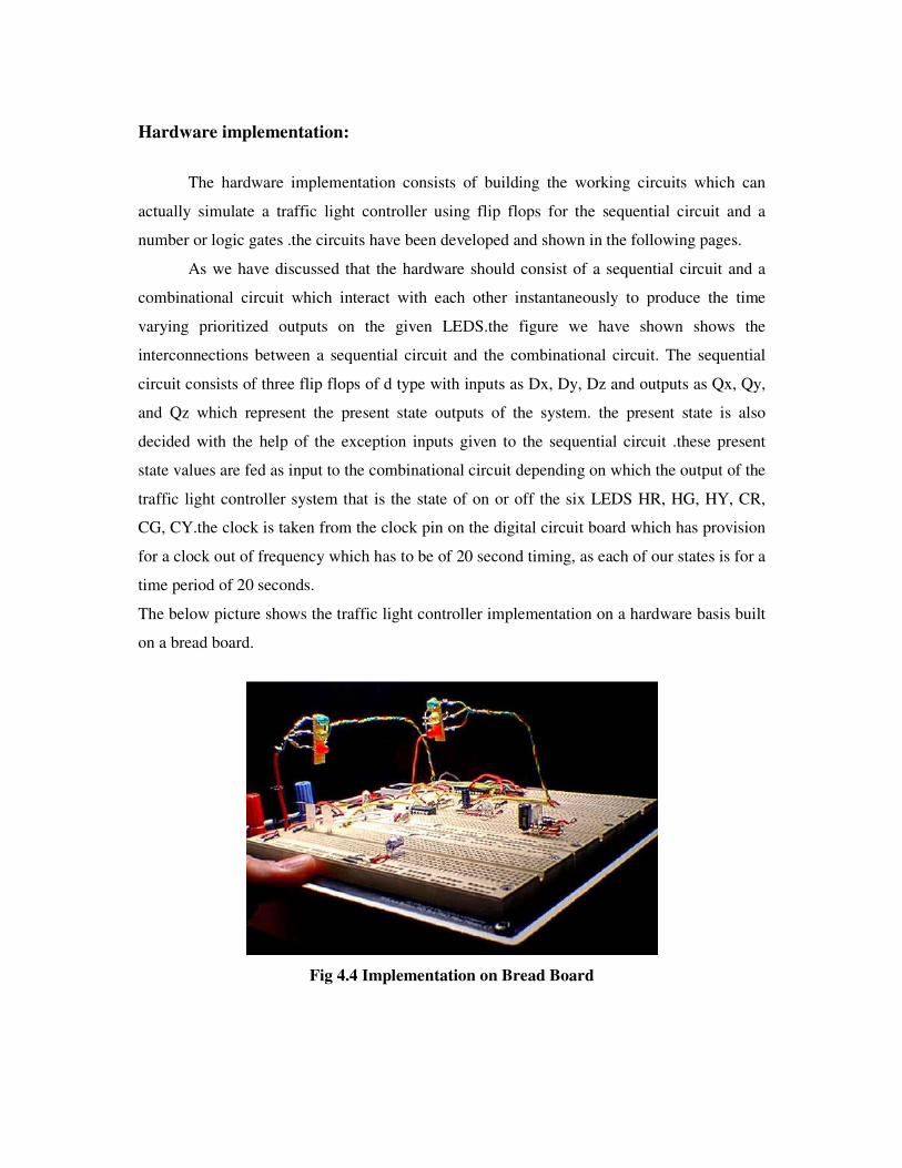
Hardware implementation:
The hardware implementation consists of building the working circuits which can
actually simulate a traffic light controller using flip flops for the sequential circuit and a
number or logic gates .the circuits have been developed and shown in the following pages.
As we have discussed that the hardware should consist of a sequential circuit and a
combinational circuit which interact with each other instantaneously to produce the time
varying prioritized outputs on the given LEDS.the figure we have shown shows the
interconnections between a sequential circuit and the combinational circuit. The sequential
circuit consists of three flip flops of d type with inputs as Dx, Dy, Dz and outputs as Qx, Qy,
and Qz which represent the present state outputs of the system. the present state is also
decided with the help of the exception inputs given to the sequential circuit .these present
state values are fed as input to the combinational circuit depending on which the output of the
traffic light controller system that is the state of on or off the six LEDS HR, HG, HY, CR,
CG, CY.the clock is taken from the clock pin on the digital circuit board which has provision
for a clock out of frequency which has to be of 20 second timing, as each of our states is for a
time period of 20 seconds.
The below picture shows the traffic light controller implementation on a hardware basis built
on a bread board.
Fig 4.4 Implementation on Bread Board

The logic gate circuit for Dx
Fig 4.5 Logic Circuit for Dx

The logic gate ciruit for Dy
Fig 4.6 Logic Circuit for Dy

The logic gate circuit for Dz
Fig 4.7 Logic Circuit for Dz

Logic gate circuitry for the combinational design
Fig 4.8 Logic Circuit for Combinational Design

Disadvantages of the hardware design of the traffic light controller and the reason
behind going for FPGA based embedded system.
The hardware design as we have seen till now has turned out to be very big in size
because of the number of transistors involved in the design. Also the huge number of circuits
involved creates the problem of additional delays which can turn out to be fatal while dealing
with a traffic light controller. There again is the problem of driving capabilities of the circuits
because of the huge number of devices involved the current required may be higher and
unsupported by our system. The hardware design as we see has become big enough to be said
to cumbersome and confusing and fault occurring in any part of the circuit can cause the
whole circuit to become obsolete as fault finding and correction is very difficult process
because of the vastness involved in the circuit. such a hardware design can not be
implemented for practical purposes where generally we need to have systems with specific
and precise output response .therefore we go for a FPGA based Embedded system
development for a traffic light controller which is nothing more than a completely
programmed chip which is optimized to reduce the delays involved and implements all the
advantages of a FPGA on to a traffic light controller system which now can be used in
practical situations with almost absolute accuracy and precision. The FPGA programmed
now acts like a controller which can be placed at some possible point of operation and runs
continuously without any errors.

Chapter 5
OVERVIEW OF SPARTAN-2
The Spartan 2 design kit is an easy-to-use evaluation board for the DS33Z11 Ethernet
transport-over-serial link device. The Spartan 2 is intended to be used with a resource card for
the serial link. The serial link resource cards are complete with transceiver, transformers, and
network connections. Dallas’ Chip View software is provided with the design kit, giving
point-and-click access to configuration and status registers from a Windows®-based PC. On-
board LEDs indicate receive loss-of-signal, queue overflow, Ethernet link, Tx/Rx, and
interrupt status.
FEATURES
� Demonstrates Key Functions of DS33Z11 Ethernet Transport Chipset
� Includes Resource Card with DS21348 LIU, DS2155 T1E1 SCT, and DS3170 T3E3
SCT, Transformers, BNC and RJ48 Network Connectors and Termination
� Provides Support for Hardware and Software Modes
� On-Board MMC2107 Processor and Chip View Software Provide Point-and-Click
Access to the DS33Z11, DS2155, and DS3170 Register Sets
� All DS33Z11 Interface Pins are Easily Accessible for External Data Source/Sink
� LEDs for Loss-of-Signal, Queue Overflow, Ethernet Link, Tx/Rx, and Interrupt
Status
� Easy-to-Read Silk Screen Labels Identify the Signals Associated with All
Connectors, Jumpers, and LEDs
DESIGN KIT CONTENTS
• DS33Z11DK Main Board
• Single-Port Serial Card with DS2155 T1/E1 SCT, DS21348 T1/E1 LIU, and DS3170
T3/E3 SCT
• CD_ROM
• Chip View Software and Manual
• DS33Z11DK Data Sheet
• Configuration Files

Fig 5.1 Floor plan of Spartan 2
The above shows the basic layout of a Spartan 2 kit which consists various parts
which work together to produce the required results for any given application.
The basic layout consists of all the input, output, processing, and storage blocks like
the LEDS and Test point block , the SDRAM block, hardware mode switches and a serial
port for programming through a JTAG and then the main processor or FPGA part which is
interfaced with the remaining devices as shown above.

Chapter 6
TRAFFIC LIGHT EMBEDDED SYSTEM

Block Diagram of Traffic Light Embedded System:
Fig 6.1 Block Diagram of TLC
The different parts constituting the block diagram shown above are vividly below:
Input handling:
The VHDL code that implements this subsystem is located in the file trafficlight.vhd.
This file is the top level file for the entire design. Because input handling consists of several
small, unconnected tasks, I chose to implement this module as a set of processes. One process
handles the the exception request signal by providing the system with a synchronized and
latched version of the exception request input. This process also clears that internal signal
whenever the FSM instructs it to reset it. Another process is used to synchronize the go input.
In addition to synchronizing the input with the system clock, this process also ensures that the
synchronized go signal is high for at most one clock period. In other words, this process
converts levels into pulses. Doing so makes the system behave correctly independent of how
long the user presses the go push button. Finally, a third process synchronizes the reset and
traffic waiting inputs.

Timer:
The timer module is responsible for counting down a specified number of seconds and
informing the FSM when that allotted time has expired. The VHDL source code for this
module is listed at the end. The timer has a 4-bit input connected to the RAM data bus and
produces an expired signal indicating when the amount of time specified by the RAM has
elapsed. It relies on the once per second pulse that the enable signal provides in order to
increment an internal count once every second. When that count reaches the value specified
by the RAM, the timer resets its internal counter to zero and brings the expired output signal
high. This design allowed me to eliminate the start timer signal from the timer module.
Because the timer resets itself automatically to zero whenever it brings the expired signal
high, this design doesn’t have to worry about synchronizing the start timer signal between the
FSM and the timer module.
Divider:
In order to generate the one second clock needed for effective operation of the traffic light,
we needed to divide down the 4 MHz system clock to around 0.05 Hz by a factor of
80,000,000. We did so using two modules called clock generator and divider. The clock
generator unit uses the 4 MHz system clock to synthesize a 0.05 Hz pulse clock. In other
words, it generates a signal that is high for one clock period out of every 80000 clock periods.
Originally, we had planned to use this signal as the clock signal for many other components
in the system (hence the name “clock generator”). However, I’ve since found that to be
unnecessary and instead use the system clock. This module is implemented with a 26 bit
counter that counts down by one every clock cycle. Whenever the counter reaches zero, the
slow clock output goes high for one cycle. The divider module is used to further divide down
the system clock. Starting with the 0.05 Hz pulse provided by the clock generator module, it
generates an output signal that is high for exactly one period out of every 80,000,000 clock
cycles. In other words, the divider module’s output is high for one clock cycle per 20
seconds. The divider contains an 26 bit counter that counts down from a fixed value. That
value is 2^26 in decimal (or”11111111111111111111111111” in binary), which is exactly
the value needed to generate one pulse every 20 second.

Outputs:
The storage and output module contains the HEX-LED used to display the
alphanumeric value of the system’s timing parameters and the RAM used to store those
parameters. Using the HEX-LED display on the Spartan kit was done. We used the pin
numbers attribute in my top level VHDL source file to force the VHDL compiler to place the
data lines for the RAM data bus on a particular set of pins. Those pins corresponded to the
data lines A0 through A3. Once I enabled a few control signals Spartan, the lab kit displayed
the value was on the RAM data bus using the first HEX-LED display. I used the inverted
write enable signal I was generating for the RAM as the display clock. Whenever that signal
went high, the RAM was writing data to the bus (i.e. a read cycle was being executed).
During the course of designing and building this traffic light controller, we encountered
several problems and errors. These included being unable to fit my design into the FPGA,
having my FSM transition into unexpected states at unexpected times, and having the system
occasionally not see the expired signal generated by the timer module.
Design Problems:
We original design was based on a pair of counters much like those found in the clock
code given later and divider modules. These counters would produce a clock signals that
oscillated at a much lower frequency than the system clock. we planned on having most of
the system being driven by the one kilohertz clock that came from the clock generator
module while the timer was to be sourced using the one hertz clock from the divider module.
This design would have worked had we used LSI chips to implement it, but didn’t work when
placed into the FPGA. The problem was that the FPGA uses a very specialized path for clock
signals to all of its flip flops. This makes it difficult to route internally generated signals to
the clock inputs of other components on the same FPGA.
After lot of attempts we noticed that the clock frequency of the FPGA has to be
considered and so output of the clock generator and divider modules as enable signals. The
FPGA hardware is able to route and generate flip flop enable signals much better than clock
signals. To do so, we had to change the divider and clock generator modules to produce
outputs that were pulses rather than levels, since the components that depended on them
would need to be active for only once cycle out of many. These changes simplified the design
and allowed the entire thing to fit in a single FPGA.

State Machine Problems:
Initially, our FSM was appeared to transition into the wrong states at the wrong times.
We attempted to add a test output to my design so that we could view the present state signal
on the logic analyzer. But since we was using automatically generated state assignments at
the time, we couldn’t do so. Eventually, I rewrote my FSM code to use hard coded states
assignments so that we could more easily view the current state signal using the logic
analyzer. This helped a great deal. After doing this, we was able to fix several design and
implementation bugs.
Timing Problems:
The next major problem was in correctly handling the expired and starts timer signals.
We found that because the expired signal was updated only once per second, whenever it
went high, it would force a state transition as expected. But because it remained high for
considerable timer after, the next state to be entered would transition to its next state as well.
This process would repeat until enough time had passed for the expired signal to go low. In
the meantime, the system would go crazy. Our solution to this problem was to have the FSM
convert the expired signal from a level to a pulse internally. That way, regardless of how long
the timer kept expired high for, the FSM would only see its internal version of expired high
for exactly one clock cycle. The start timer signal that the FSM generates to force the divider
module to reset its count is simply a delayed version of the internal expired signal.
The simulator:
We were using the xilinx 8.2 ISE simulator for the testing and code building purpose. the
simulator had too many functionalities to know all and so we had to get completely
acquainted with the simulator before starting of and the debugging process to was a tough
because the simulator we felt is not that user friendly as it does not give proper solution to
many errors which are internal in nature and not related to the code. initially we had to check
the working of the code on state machines on test bench rather a hardware platform ,this
created even more problems because the test bench this simulator offers is a completely
different one and many times we had to write the code for test bench as it was not being
created directly.

Chapter 7
RESULTS OF TLC

Results of Traffic Light Control:
Fig 7.1 Test-Bench for Clock Divider:

Fig 7.2 Test-Bench for four bit Clock divider:

Fig 7.3 Test-Bench Waveform when SH=0, SG=0:

Fig 7.4 Test-Bench Waveform when there is an exception in SG=1, SH=0 during divided
clock period:
SG=1, SH=0
CG=1, HR=1 Change in waveform

Fig 7.5 Test-Bench Waveform when there is an exception in SG=0, SH=1 during divided
clock period:
SG=0, SH=1
CR=1, HG=1 Change in
waveform

Chapter 8
DESIGN-2
SPEECH ENCRYPTION AND DECRYPTION

Introduction:
SPEECH encryption has always been a very important part of military
communications. Today, due to the fast development of computer technologies,
microprocessors, integrated circuits, LSI and VLSI, modem cryptography, etc., speech
encryption techniques have entered a completely new era. Technically speaking, digital
encryption of speech is always the best approach, in which the original speech signal x is first
digitized into a sequence of bits, x (k) which are then encrypted digitally into a different
sequence of bits, y (k) before transmission. Digital transmission is always much more
efficient than analog transmission, and it is much easier for digital encryption techniques to
achieve a very high degree of security. Of course, this type of technique is still not quite
compatible with today’s technical environment, i.e., most of the telephone systems are still
analog instead of digital; most practical speech digitizers still require a relatively high bit rate
which cannot be transmitted via standard analog telephone channels; and low bit-rate speech
digitizers still imply relatively high complexity and poor quality.
Furthermore, almost all techniques of this type require accurate synchronization
between the transmitter and the receiver, i.e., exactly the same block of bits has to be
processed by the encryption and decryption devices for signal recovery. The synchronization
problem becomes the essential part of the implementation of such techniques. This not only
tremendously worsens the complexity, but makes the transmission much more sensitive to
channel conditions because slight synchronization error due to channel impairment can
completely break the transmission. There is another type of speech encryption technique
called scrambling. The original speech signal x is scrambled directly into a different signal y
(t) in analog form before transmission.
The encryption is represented by the transformation between x(t) and y(t) regardless
of digitization. Since the scrambled signal is analog, with similar bandwidth and
characteristics as the original speech signal, this type of technique is more compatible with
today’s technical environment, i.e., can be easily used with existing analog telephone
systems. Some conventional techniques of this type, such as frequency inversion and band
splitting, do not require synchronization at all for transmission. Although they have been very
useful historically, these not true any longer, lately due to the low degree of security
achievable. A new series of techniques of this type, the sample data scrambling, have been
developed and used extensively in recent years, since it can preserve the advantages of

scrambling techniques while tremendously improving the degree of security. A typical block
diagram of such techniques is shown. The original speech x is first sampled into a series of
sample data, x(n). Then scrambled into a different series of sample data, y (n) and recovered
into a different signal y ( t ) for transmission.
These techniques have a relatively high degree of security and are compatible with
today’s technical environment, thus, they are very useful in the present time. However,
almost all these techniques also require synchronization between transmitter and receiver,
because the transformation from x (n) into y (n) has to be performed frame by frame, and
exactly the same frame of sample data has to be used in the scrambling and descrambling
processes for correct signal recovery. This again complicates the implementation and makes,
the transmission very sensitive to channel conditions.
Recently, two new sample data scrambling techniques have been proposed. One
scrambles the speech in frequency domain, and the other in time domain; both approaches
preserve the advantages of the sample data scrambling, while eliminating the requirement for
synchronization. In other words, no synchronization is required in the receiver at all. This not
only simplifies the system structure, but significantly improves the feasibility and reliability
of sample data scrambling techniques. The basic point here is that the synchronization is
necessary as long as the scrambling and descrambling are performed frame by frame. It
becomes unnecessary when “frame” is not defined in the operation. Efficient speech
encryption technique is required for recent communication, not only over digital but also
analogue data transmission lines without invasion of privacy. Two types of speech encryption
scheme have been proposed.
The former type is the frequency bands swapping of analogue signal. The method can
be used for wide variety of analogue and digital application systems since the method can
transmit speech signal over standard telephone line with acceptable speech quality.
According to the result of psycho acoustical evaluations, context of speech is suspected due
to remained envelop information of speech. The latter method is the digital speech signal
encrypted. It is based on redundant bit to protect speech information effectively. Although the
method is secure, it is hard to apply the method to conventional analogue transmission line
because the bandwidth is wide. In order to reduce the bit rate under the bandwidth for
analogue line, a speech encryption system with a low bit rate coding algorithm is necessary.

Speech can be described as an act of producing voice through the use of the vocal folds
and vocal apparatus to create a linguistic act designed to convey information.
1. Various types of linguistic acts where the audience consists of more than one
individual, including public speaking, oration, and quotation.
2. The physical act of speaking, primarily through the use of vocal cords to produce
voice. See phonology and linguistics for more detailed information on the physical act
of speaking.
However, speech can also take place inside one's head, known as intrapersonal
communication, for example, when one thinks or utters sounds of approval or disapproval. At
a deeper level, one could even consider subconscious processes, including dreams where
aspects of oneself communicate with each other (see Sigmund Freud), as part of intrapersonal
communication, even though most human beings do not seem to have direct access to such
communication.

Chapter 9
FUNDAMENTALS OF
ENCRYPTION AND DECRYPTION

INTRODUCTION:
Cryptography refers to the science of transforming messages to make them secure
and immune to attacks. Alternatively cryptology is the study of mathematical techniques for
attempting to defeat (Attack) cryptographic techniques and, more generally information
security services so for the message to be secured and immune to attack we need to encrypt
our message at the sender site and decrypt at receiver site.
Now days the modern advanced concept of this technology is used which is known
as public key cryptography. This method has been devised suitably that uses two keys: one
public and another are private.
The components involved in cryptography are
i) Sender
ii) Receiver
iii) Plain text
iv) Cipher text
v) Encryption and decryption algorithms
vi) Network.
Fig 9.1 Block Diagram for Standard Encryption and Decryption
� The original message before being transferred is called, plaintext.
� The message after being transferred is called, cipher text. This message contains all
the information of the plaintext message but is not in a format readable by a human or
computer without the proper mechanism to decrypt it.
� The Algorithm which transfers a plain text to cipher text is called Encryption
algorithm.
Sender Receiver
Plain text Plain text
Cipher text
Encryption Network decryption Encryption Network Decryption
Sender Receiver
Plain text Plain text
Cipher text
Encryption Network decryption Encryption Network Decryption

� And the algorithm which transfers cipher text to plain text is called Decryption
algorithm.
� Encryption algorithm is used by sender.
� Decryption algorithm is used by receiver.
The different categories of cryptography algorithms such as encryption and
decryption are referred as cipher. A cipher is an algorithm for performing encryption (and
the reverse, decryption). The sender-receiver pair in a network uses the cipher for a secure
communication. A key is a number or a piece of information as an algorithm upon which
the cipher operates. Hence for the encryption of a message we need an encryption algorithm,
an encryption key, and plain text. Similarly to decrypt a message we need a decryption
algorithm, a decryption key, and cipher text.
Fig 9.2 Following figure shows the idea about encryption and decryption of messages.
Plain text cipher text
Encryption Key
EncryptionAlgorithm
EncryptionAlgorithmPlain text cipher text
Encryption Key
EncryptionAlgorithm
EncryptionAlgorithm
Cipher text Plain text
Decryption Key
DecryptionAlgorithm
DecryptionAlgorithmCipher text Plain text
Decryption Key
DecryptionAlgorithm
DecryptionAlgorithm
a. Encryption b. decryption
Types of cipher
There are a variety of different types of encryption. Algorithms used earlier in the
history of cryptography are substantially different from modern methods, and modern
ciphers can be classified according to how they operate and whether they use one or two
keys.
All the Encryption method of cryptography algorithms are divided into two groups:
i) symmetric-key cryptography algorithms (private key cryptography)
ii) public-key cryptography algorithms
In the cryptography the encryption and decryption algorithms are public but the key is secret.
Only the key need to be protected rather than the encryption and decryption algorithms.

SYMMETRIC-KEY CRYPTOGRAPHY:
In symmetric-key cryptography, a common key is shared by both sender and receiver.
The sender uses an encryption algorithm and the same key to encryption of data and the
receiver uses a decryption algorithm and the same key for the decryption of data. In this
process of cryptography the algorithm used for decryption is reverse of encryption algorithm.
The shared key set up in advance and kept secret from all other parties.
Sender Receiver
Plain text Plain text
Cipher text
Encryption Network decryptionEncryption Network Decryption
shared secret key
Sender Receiver
Plain text Plain text
Cipher text
Encryption Network decryptionEncryption Network Decryption
Sender Receiver
Plain text Plain text
Cipher text
Encryption Network decryptionEncryption Network Decryption
shared secret key
Fig 9.3 Symmetric –Key Cryptography System
Advantages of Symmetric key cryptography algorithm:
� It takes a less time to encrypt a message using symmetric key algorithm than a
message using public key algorithm.
� The key is usually smaller so symmetric key algorithms are used for to encrypt and
decrypt long messages.
Disadvantage
� Each pair of user must have an unique key
� So a large number of keys are required, hence distribution of keys between two
parties can be difficult.
Symmetric-key algorithms can be divided into traditional ciphers and block ciphers.
Traditional ciphers encrypt the bits of the message one at a time. The unit of data that can be
encrypted at a time is only one bit. And block ciphers take a number of bits and encrypt them
as a single unit. Blocks of 64 bits have been commonly used. And now days a block of 128
bits can be encrypted by some advanced encryption standard algorithms.

Data encryption standard (DES)
Data encryption standard is a complex block cipher which consists s-box and p-box.
This algorithm encrypts a 64-bit plaintext using a 56-bit key. It is the most widely used
encryption scheme. It is a block cipher and longer plaintexts can be processed using 64-bit
blocks. The text is put in 19 different complex procedures to create a 64-bit key. It consists of
two transposition blocks, one for swapping and another is a 16-bit complex block called
iteration block.
Fig 9.4 A Model of DES
Some basic operation modes of the DES
To encrypt and decrypt longer messages several operation modes of the DES
algorithms are defined
Electronic code block (ECB) mode
In this type of operation mode long messages are divided into several blocks and
encryption of each block is carried out individually, where each block contains 64-bits of data
as a unit. The encryption of each block is independent of other blocks.
Fig 9.5 ECB Mode of DES

Cipher block chaining (CBC)
In CBC mode the encryption of a block depends on all previous blocks. To encrypt
the second plaintext (P2), we first XOR it with the first ciphertext (C1) and pass it through
the encryption process and so on.
Fig 9.6 CBC Mode OF DES
Cipher feedback mode (CFM)
Cipher feed back mode is suitable for the situation where we require to send or
receive 1 byte of data at a time. The 1 byte cipher text CN depends upon 1 byte plaintext PN.
Fig 9.7 CFM Mode of DES
Cipher stream mode (CSM)
Like CFM it encrypts or decrypt 1 bit at a time but at the same time the next bit is
independent upon previous bit. Data are XORed bit by bit with a long, one-time bit stream
that is generated by an initialization vector in a looping process.
Fig 9.8 CSM Mode of DES

Chapter 10
OVERVIEW OF VIRTEX II PRO

Virtex II Pro:
General Description:
The Virtex-II Pro and Virtex-II Pro X families contain platform FPGAs for designs
that are based on IP cores and customized modules. The family incorporates multi-gigabit
transceivers and PowerPC CPU blocks in Virtex-II Pro Series FPGA architecture. It
empowers complete solutions for telecommunication, wireless, networking, video, and DSP
applications. The leading-edge 0.13 µm CMOS nine-layer copper process and Virtex-II Pro
architecture are optimized for high performance designs in a wide range of densities.
Combining a wide variety of flexible features and IP cores, the Virtex-II Pro family enhances
programmable logic design capabilities and is a powerful alternative to mask-programmed
gate arrays.
Architecture Overview:
Virtex-II Pro and Virtex-II Pro X devices are user-programmable gate arrays with various
configurable elements and embedded blocks optimized for high-density and high-
performance system designs. Virtex-II Pro devices implement the following functionality:
� Embedded high-speed serial transceivers enable data bit rate up to 3.125 Gb/s per
channel (RocketIO) or 6.25 Gb/s (RocketIO X).
� Embedded IBM PowerPC 405 RISC processor blocks provide performance up to 400
MHz.
� SelectIO-Ultra blocks provide the interface between package pins and the internal
configurable logic. Most popular and leading-edge I/O standards are supported by the
programmable IOBs.
� Configurable Logic Blocks (CLBs) provide functional elements for combinatorial and
synchronous logic, including basic storage elements. BUFTs (3-state buffers)
associated with each CLB element drive dedicated segmentable horizontal routing
resources.
� Block SelectRAM+ memory modules provide large 18 Kb storage elements of True
Dual-Port RAM.
� Embedded multiplier blocks are 18-bit x 18-bit dedicated multipliers.

Digital Clock Manager (DCM) blocks provide self-calibrating, fully digital solutions for
clock distribution delay compensation, clock multiplication and division, and coarse- and
fine-grained clock phase shifting. A new generation of programmable routing resources
called Active Interconnect Technology interconnects all these elements. The general routing
matrix (GRM) is an array of routing switches. Each programmable element is tied to a switch
matrix, allowing multiple connections to the general routing matrix. The overall
programmable interconnection is hierarchical and supports high-speed designs.
All programmable elements, including the routing resources, are controlled by values
stored in static memory cells. These values are loaded in the memory cells during
configuration and can be reloaded to change the functions of the programmable elements.

Chapter 11
DEVELOPMENT OF ENCRYPTING
AND DECRYPTING SYSTEM

Methodology:
Simulation Procedures:
In this project we have worked out two simulations processes:
1. Offline Simulation using Xilinxs 9.1i project navigator
2. Online Simulation using Virtex II Pro platform FPGA
Offline process:
Offline simulation process is shown below. Offline process does not include hardware
implementation. Offline process is only for self test of encryption/decryption algorithm. After
successful testing of encryption/decryption algorithm we will go for online process.
Fig 11.1 Offline Process
The process is discussed in the following steps:
� In the recording process firstly we take voice as source input. Then using matlab
created a text (.txt) file. The parameters given during creation of .txt file are voice
duration and its bit rate. The matlab code for conversion of speech (.wav file) to text
(.txt) file was written.

� After successfully creating text file, the test bench will read this text file character by
character and then these values will be mapped with the process written for
encryption/decryption.
� After encryption/decryption operation has performed the text bench will again create
a text file but this text file contains encrypted version of voice.
� In the final step matlab code again read the encrypted version of text file and plays it
at the specified bit rate.
Online Process:
Online process includes software as well as hardware implementation. The board on
which the VHDL code is burned is already discussed in the previous chapter. The board
contains in-built ADC/DAC ports. So the VHDL code written at the transmitting end
performs two operations:
� Conversion of analogue voice into digital data by ADC converter
� Use of symmetric-key cryptography for encryption
� Finally the encrypted values are sent to the outside world via DAC converter.
Similarly at the receiver end code performs:
� Analog to digital conversion
� Standard decryption algorithm
� Digital to analog conversion
Fig 11.2 Online Process
Channel / Medium

The online process is a real time process. Here input comes continuously from the mic
input, this input is given to the ADC converter of Virtex II Pro board. Here we preferred
symmetric-key cryptography for encryption because here the same code performs both
encryption and decryption operations. In symmetric-key cryptography, a common key is
shared by both sender and receiver. The sender uses an encryption algorithm and the same
key to encryption of data and the receiver uses a decryption algorithm and the same key for
the decryption of data. In this process of cryptography the algorithm used for decryption is
reverse of encryption algorithm. The shared key set up in advance and kept secret from all
other parties.
Sender Receiver
Plain text Plain text
Cipher text
Encryption Network decryptionEncryption Network Decryption
shared secret key
Sender Receiver
Plain text Plain text
Cipher text
Encryption Network decryptionEncryption Network Decryption
Sender Receiver
Plain text Plain text
Cipher text
Encryption Network decryptionEncryption Network Decryption
shared secret key
Fig 11.3 Symmetric-Key Cryptography System
Here Stream Cipher of Data Encryption Standard algorithm is used. Stream cipher is a
class of ciphers in which encryption or decryption is done using separate keys which are
generated using some key generating function. On the other hand block ciphers are ones in
which a single key is used throughout encryption and decryption.
In our context the key space consists of 30 different keys for a 30 data sample and the
key space repeats itself for the subsequent data samples. Also a shift algorithm is used to
obtain these 30 different keys. Algorithm consists of generation of key space and X-ORing of
this key space with 30 data samples is designed, simulated, implemented on an FPGA and
finally the hardware is tested. Here the keys used for encryption/decryption is of 14 bit each.
Since ADC gives 14 bit output so our keys are confined to 14 bit. But the DAC which is
present on Virtex II Pro takes 12 bit input, so we are neglecting two MSB bits of the ADC
output. Then the DAC sends encrypted version of speech to the out side world. The codes for
performing all these are given in the next chapter.

Discussion for Speech Encryption and Decryption:
OFFLINE Process: In this process as we have discussed before we used MATLAB for recording and
playing Audio or Speech and storing the recorded speech in a text file and playing a speech
waveform by reading it from a text file. All these operations were done with the help of
appropriate MTLAB codes that write to and read from a text file.
Then we have written the required VHDL codes, one for Speech Encryption and
Decryption procedure and the others for reading the text file we have generated through
MATLAB through the Test-Bench in Xilinx and writing of the encrypted data values we get
from the speech encryption/decryption part into a text file through a Test-bench which can be
played in MATLAB by using previously said code which plays a speech file from a text file.
Here we observed that more the number bits we take to represent the discrete values of a
sampled speech signal, the more is the clarity of the speech and more complex algorithm is
required for its encryption. In our code we have used 12 bit representation for each sample
value and taken 20 samples at a time for encryption with 20 different random bit sequences.
ONLINE Process:
In this process first of all we have programmed the ADC/DAC converters available
on the Virtex II Pro board to sample the incoming analog speech signal at a sampling
frequency of 1MHz then once we have the sampled data value of the speech signal we
encrypt it using a random bit sequence and we have taken a 20 state code for our purpose of
having key space of 20 random bit sequences. This encrypted data value is simultaneously
sent through a DAC to speakers. For decryption since we have used a XORing operation as
our encryption scheme we can use the same code we have developed. The ADC output is of
14bit number where as DAC input had to be 12 bit so we had to for the conversion of the
14bit input number to a 12 bit number by rounding of the two LSBs.

Chapter 12
CONCLUSION

Conclusion:
FPGAs offer all of the features needed to implement most complex designs. Clock
management is facilitated by on-chip PLL (phase-locked loop) or DLL (delay-locked loop)
circuitry. Dedicated memory blocks can be configured as basic single-port RAMs, ROMs,
FIFOs, or CAMs. Data processing, as embodied in the devices’ logic fabric, varies widely.
The ability to link the FPGA with backplanes, high-speed buses, and memories is afforded by
support for various single ended and differential I/O standards. Also found on today’s FPGAs
are system-building resources such as high speed serial I/Os, arithmetic modules, embedded
processors, and large amounts of memory.
Here in our project we have tried to implement such powerful FPGAs in the design of
possible embedded systems that can be designed, burned and deployed at the site of operation
for handling of many kinds of applications. In our project we have basically dealt with two of
such applications –one the prioritized traffic light controller and other a speech encrypting
and decrypting system.
Our first design was the traffic light controller and optimal traffic signal settings at a
signalized intersection can minimize the vehicle delay time, stops, and queue length at a stop
line. They can also save fuel, decrease overall emissions, and improve the overall standards
of living, especially in urban areas. The development of an appropriate phase plan for a given
intersection is an important aspect of any traffic signal system design. Simulation analysis of
such systems can provide cost-effective and optimum designs. However, other performance
metrics should also be considered when designing such systems, including safety,
intersection capacity, and location of intersection. The traffic engineer/planner should apply
knowledge and understanding of various phasing options and how they affect critical aspects
and goals of the required signaling.
In this report, we’ve described the requirements, design, and implementation process
for our traffic light controller. We started by describing the requirements for the traffic light
controller. These requirements included the ability of having a functional user interface
allowing the system operator to examine and change the configuration of the system, and the
ability to follow a complex lighting protocol whose exact behavior in any given iteration
depended heavily on external inputs. Those requirements, in turn, introduced several
challenges. The reliance on dynamic external inputs necessitated the introduction of complex
synchronization hardware. Likewise, the need to have the system operate in multiples of one

second required a great deal of design and debugging time, in addition to a large amount of
hardware resources.
The end result of our design, implementation, and debugging work is a controller
implementation that satisfied all aspects of the protocol described earlier, and in general met
all the of the specifications necessary for a traffic light controller. All in all, the design is
robust. There are no ‘hack’ solutions, and all the design decisions were scrutinized
thoroughly before implementation. Overall, the design and implementation of the traffic light
controller is a good first step in designing more complex system. It stressed the importance of
designing subsystems one at a time and drew attention to various control, data path, and
timing issues common in large digital systems.
Then we went for the development of a embedded system that can properly interface
with an offline and online audio input that is read the signal and write it and then using a fpga
which is capable of fast processing implement a cryptographic algorithm that encrypts the
voice data or the output of the ADC and then sends it for transmission and at the receiving
side we have developed a similar kind of embedded processor that takes care of the
decrypting process and gives out the decrypted signal. Voice encryption units and speech
scramblers both suffer several drawbacks. The largest problem with any communications
security device is that a unit is required at each end of the conversation for the system to
work; so unless you're prepared to sacrifice some of your privacy by making unencrypted
calls you'll swiftly end up broke. Any method of securing against eavesdropping is expensive
(scramblers start at around $100 and encrypting telephones can range into the thousands).
Many such implementations are possible wherein we try to build robust embedded
processors for the purpose of controlling and handling of variety of tasks implementing all
the features of an FPGA into the system making the system robust, precise and accurate. Here
we have made two such embedded systems that deal with traffic light controllers and speech
cryptography as a part of our work.

References:
[1] Digital design: Morris Mano M
[2] Digital design: Frank Vahid
[3] Roess, R. P., and W. R. McShane. 1998. Traffic engineering. 2d ed. Engelwood Cliffs,
NJ: Prentice Hall.
[4] Clement, S., and J. Koshi. 1997. Traffic signal determination: The cabal model. 1997
Genetic Algorithms in Engineering Systems: Innovations and Applications Conference, pp.
63-68.
[5] McShane, W., and R. Roess. 1990. Traffic engineering. Engelwood Cliffs, NJ: Prentice
Hall.
[6] Kuwahara, M., and M. Koshi. 1990. Decision of timings of signal program switching in
pretime multi-program control. In Transportation and traffic theory, edited by M. Koshi,
531-50. New York: Elsevier.
[7] Nakats, T., S. Seki, S. Shibliya, and I. Tkaku. 1994. Artificial intelligence approach for
optimizing traffic timings on urban road networks. Proceedings of the 1994 Vehicle
Navigation and Information Systems Conference, pp. 199-202.
[8] Wilshire, R., R. Black, R. Grochoske, and J. Higinbotham. 1985. Traffic control systems
handbook. FHW A-IP-85-12. Washington, DC: Federal Highway Administration, U.S.
Department of Transportation.
[9] H. J. Beker and F. C. Piper, Secure Speech Communications. London, U.K.: Academic,
1985.
[10] B. Goldburg, S. Sridharan, and E. Dawson, “Design and cryptanalysis of transform-
based analog speech scramblers,” IEEE J. Select. Areas Commun., vol. 11, no. 5, pp. 735–
744, May 1993.
[11] A. Matsunaga, K. Koga, and M. Ohkawa, “An analog speech scrambling system using
the FFT technique with high-level security,” IEEE J. Select. Areas Commun., vol. 7, no. 4,
pp. 540–547, Apr. 1989.
[12] K. Li, Y. C. Soh, and Z. G. Li, “Chaotic cryptosystem with high sensitivity to parameter
mismatch,” IEEE Trans. Circuits Syst. I, Fundam. Theory Appl., vol. 50, no. 4, pp. 579–583,
Apr. 2003.
[13] G. Manjunath and G. V. Anand, “Speech encryption using circulant transformations,”
Proc. IEEE Int. Conf. Multimedia and Expo, vol. 1, pp. 553–556, 2002.