Embed Size (px)
Citation preview

DUALEH ET AL. VOL. 8 ’ NO. 1 ’ 362–373 ’ 2014
www.acsnano.org
362
December 16, 2013
C 2013 American Chemical Society
Impedance Spectroscopic Analysisof Lead Iodide Perovskite-SensitizedSolid-State Solar CellsAmalieDualeh, ThomasMoehl,*Nicolas Tetreault, Joel Teuscher, PengGao,MohammadKhajaNazeeruddin,
and Michael Gratzel*
Institute of Chemical Sciences and Engineering, Laboratory of Photonics and Interfaces, �Ecole Polytechnique Fédérale de Lausanne, Lausanne, Switzerland
The growing demand for renewableenergy sources has led to considerabledevelopment in many areas related to
the research and manufacture of solar cells.In an effort to generate more cost-effectivetechnology, the field of thin film solar photo-voltaics presents a promising avenue towardhigh efficiency solar energy conversion.The third generation solar cells combine
diverse concepts and materials for the effi-cient harvest of sunlight. Purely organicdevices as well as the electrochemical solarcells (i.e., dye-sensitized solar cells, DSCs)and quantum dot solar cells with their solid-state counterparts show promising resultsand are partly already in the first stages ofemerging into the market. Though thesetypes of solar cells are diverse in materialsand design, they have one idea in common.They all possess a high extinction coefficientabsorber (molecular quantum dot or a thinabsorber layer) at a heterointerface. Nor-mally, the heterointerface has a high surfacearea to increase absorption while maintain-ing a thin absorber layer.
With the publication by Im et al.1 in 2011,the research of lead-based perovskites aspotential high extinction light absorbersin solar cells intensified, while Chung et al.2
demonstrated, in addition to the light-absorbing properties, the hole transportcapabilities of a closely related perovskitematerial. The subsequent publications ofKim et al.3 and Lee et al.4 in 2012 reportedhigh efficiency solid-state devices using thelead halide perovskite system on conduc-tive and insulating mesoporous substrates.Important to note here is the uniqueness
of the mixed-halide perovskite utilizedby Lee et al.4 and Ball et al.5 In this case,perovskite is deposited from a mixture indimethylformamide-containing PbCl2 andCH3NH3I and was shown to behave as bothelectron and hole transport material. As isseen from the work presented by Ball et al.,5
the perovskite forms a compact overlayeron top of the mesoporous metal oxidescaffold of approximately 250 nm.The system investigated here uses
a similar lead-iodide-based perovskite as
* Address correspondence [email protected],[email protected].
Received for review August 19, 2013and accepted December 16, 2013.
Published online10.1021/nn404323g
ABSTRACT Mesoscopic solid-state solar cells based on the inorganic�organic
hybrid perovskite CH3NH3PbI3 in conjunction with the amorphous organic
semiconductor spiro-MeOTAD as a hole transport material (HTM) are investigated
using impedance spectroscopy (IS). A model to interpret the frequency response of
these devices is established by expanding and elaborating on the existing models
used for the liquid and solid-state dye-sensitized solar cells. Furthermore, the
influence of changing the additive concentrations of tert-butylpyridine and LiTFSI in
the HTM and varying the HTM overlayer thickness on top of the sub-micrometer
thick TiO2 on the extracted IS parameters is investigated. The internal electrical
processes of such devices are studied and correlated with the overall device
performance. In particular, the features in the IS responses that are attributed to
the ionic and electronic transport properties of the perovskite material and manifest as a slow response at low frequency and an additional RC element at
intermediate frequency, respectively, are explored.
KEYWORDS: mesoscopic solar cells . perovskite . impedance spectroscopy . spiro-MeOTAD . tert-butylpyridine . LiTFSI
ARTIC
LE

DUALEH ET AL. VOL. 8 ’ NO. 1 ’ 362–373 ’ 2014
www.acsnano.org
363
light-absorbing material in a solid-state mesoscopicheterojunction style solar cell employing the amor-phous organic p-type semiconductor 2,20,7,70-tetrakis-(N,N-di-p-methoxyphenylamine)-9,90-spirobifluorene(spiro-MeOTAD) as the hole transport material (HTM).The lead iodide perovskite in this work is depositedby spin-coating from a 1:1 molar ratio solution of PbI2and CH3NH3I in γ-butyrolactone (GBL) directly ontothe mesoporous TiO2 films following the procedurereported by Kim et al.3 These films are subsequentlyannealed at 100 �C for 10 min, leading to the forma-tion of the inorganic�organic lead-iodide-based per-ovskite, CH3NH3PbI3 crystallites.While Lee et al.4 showed that a mixed-halide perov-
skite on a mesoporous Al2O3 photoanode acts as bothlight absorber and electron conductor, Etgar et al.6
showed that the pure iodide perovskite can act as ahole conductor. Similar to Etgar et al., Chung et al.2
showed that a similar perovskite material, CsSnI3,functions as a hole conductor.This demonstrates the intriguing property of perov-
skites in that they do not only act as light absorbersbut participate in the charge conduction. Furthermore,the perovskite halides do not only possess electroniccharge conduction but might additionally exhibit ioniccharge conduction. Ionic conduction has been re-ported for perovskite-type halides such as CsPbCl3.
7
In the case of a perovskite-type oxide La2/3TiO3, lithiumion conduction has been observed when lithium ispartially substituted for Lanthanum, and the measuredconductivity was one of the highest for lithium ionconductors chemically stable at ambient atmosphericconditions.8 In this structure, 1/3 of the A sites of theperovskite structure are vacant, allowing the Li ions(which are substituted for La in A sites) to movethrough the vacancies.The ease with which these inorganic�organic hy-
brid perovskite materials can be prepared and pro-cessed from solution9,10 while simultaneously providingdesired device characteristics has made them an attrac-tive alternative in the field of electronics. The relation-ship between the organic and the inorganic com-ponents and its impact on the material structure andproperties can be exploited to design and developmaterials for targeted applications.11�13 Generally, therelatively simple organic component in these hybridstructures has been found to play a secondary role indetermining the physical properties and serve more todefine the crystal structure of the material. This is thecase for the conducting tin(II)-halide-based perovskitewhere the high conductivity arises due to the highmobility of the tin iodide sheets while the organiccomponent defines the structure.14 Alternatively, theuse of oligothiophene chromophores as the organiccomponent in combination with lead(II) halide layersallowed charge transfer between the separate compo-nents and thus not only defined the dimensionality of
the lead(II) halide layers but also determined thephotoluminescent properties of the material.12 Changet al.15 not only examined the electronic and structuralproperties of the lead-halide-based inorganic�organicperovskite CH3NH3PbX3 (X = Cl, Br, I) but also deter-mined that the physical coupling between the organicand inorganic components is weak, allowing easyrotation of the organic CH3NH3 constituent.A further advantage of these materials is the relative
ease with which their light-harvesting capabilities canbe tuned by chemical management as shown by Nohet al.16 This further allowsmore freedom and improvedmatchingbetween theperovskite and theHTMused.17�19
In order to correctly identify the role of the individ-ual components and their contribution to the deviceperformance of working solar cells, several differentsystems were investigated in addition to the completeworking perovskite-based devices. In general, it has tobe shown to what extent the behavior of the perov-skite devices shares properties with the known liquidand solid-state DSC device types and therefore to whatextent the equivalent circuits of these known devicescan be applied to the analysis of the perovskite-baseddevices. For this reason, we have investigated severalexample systems and compared them to the perov-skite devices, which included the liquid and solid-stateDSC type as well as the influence of the variation of thelithium bis(trifluoromethanesulfonyl)imide (LiTFSI) saltand tert-butylpyridine (TBP) concentration in the HTMsolution and the spiro-MeOTAD overlayer thickness ontop of the sensitized mesoporous TiO2.
RESULTS AND DISCUSSION
Considerations of the System under Investigation and Im-pedance Spectroscopy Measurement. The system underconsideration in this work shares similarities with thewell-known liquid electrolyte-based dye-sensitized so-lar cell (DSC). A DSC uses a dye as light absorber whichis adsorbed on a mesoporous TiO2 (mTiO2). The elec-tron from the light-excited dye is injected into themTiO2, transported to the back contact of the photo-anode, and collected. At the counter electrode, theelectron is then used to regenerate a redox system in aliquid electrolyte and the reduced form of the redoxsystem is transported through the electrolyte media tothe photoanode and regenerates the oxidized dye. Aclosely related device type to the DSC is a solid-stateDSC (ssDSC) in which the liquid electrolyte componentis replaced by an organic hole conductor, normallyspiro-MeOTAD. In the case of ssDSCs, the mTiO2 thick-ness is limited by the pore infiltration of the organicHTM and its short diffusion length of charge carriers.Hence, ssDSCs generally use thinner mTiO2 films of2�3 μm compared with the liquid-state alternative,which use up to 15 or even 20 μm. The perovskite-based solar cells in this work use CH3NH3PbI3 in placeof the dye sensitizers and normally also a solid-state
ARTIC
LE

DUALEH ET AL. VOL. 8 ’ NO. 1 ’ 362–373 ’ 2014
www.acsnano.org
364
HTM like spiro-MeOTAD. In these devices, the mTiO2
film thickness has been decreased further to the sub-micrometer scale, optimally between 300 and 600 nm.Due to these extremely thin film thicknesses, the porefilling with the HTM is expected to be higher and thusshould not be a limiting or irreproducible step. Relativeto solid-state or liquid DSCs, this system requiresmTiO2
films 10�30 times thinner, respectively. Consequently,the relation between the interface of the compactblocking layer/mTiO2 and the surface area of the latteris considerably altered. Hence, in the case of the systemwith sub-micrometer mesoporous TiO2 layers, theinfluence of the underlayer is muchmore pronounced.Furthermore, the interplay of the different capaci-tances (the space charge capacitance of the blockinglayer, ionic capacitances in the HTM/blocking layer andHTM/mTiO2 interfaces, and the chemical capacitanceof the mTiO2 which is relatively small due to the lowactive film thickness) will change.
Instead of a layer of dyemolecules adsorbed on thesurface of the mTiO2, like in the liquid and solid-stateDSCs, the perovskite material will cover major areas ofthe mTiO2 with layers or crystallites having thicknessesof several nanometers. The impact of the degree ofmTiO2 coverage by perovskite is unclear and a point ofmajor interest for several reasons. The recombinationof electrons from the mTiO2 with holes in the HTMmight have to involve an additional step through theperovskite. The conduction band position and/or thecharge transport in the mTiO2 can be affected eitherdue to the hindered accessibility for TBP or Liþ ions,normally crucial for the performance of especially thessDSCs, or due to the change of the ionic environmentby the perovskite coverage.
Impedance spectroscopy (IS) measurements areconducted in order to investigate the internal electricalprocesses and quantitatively and qualitatively analyzethe associated parameters. This study aims to inter-pret the IS measurements of these devices, using the
established equivalent circuits used for DSCs as astarting point and basis for the development of awell-defined model.
In general, IS is nowadays one of the most utilizedtechniques to analyze liquid DSC devices. Althoughit is a relatively long procedure from performing themeasurement over the fitting of the resulting imped-ance spectra to the analysis of the extracted data, thistechnique rewards the investigator with deep insightsabout the fabricated devices.
For a liquid DSC at intermediate and higher forwardbiases, a one-channel transmission line model is used(describing the chemical capacitance and the recom-bination and transport resistance in the TiO2) in serieswith an RC element for the counter electrode and,depending on the applied potential, a Warburg diffu-sion resistance for the ionic transport in the electrolyte(see Scheme 1a). At low forward bias when the meso-porous TiO2 is insulating, an RC element for the FTO orcompact TiO2 underlayer of the photoanode in contactwith the electrolyte has to be employed instead of thetransmission line branch for the mTiO2. A modified butsimilar model is used to simulate the impedanceresponse of ssDSCs.20,21 In the ssDSC equivalent circuit,an additional RC element has to be implementedinstead of the Warburg impedance. The additional RC(RHTM and CHTM) represents the transport of chargesinside the HTM if the hole conductor is not dopedsufficiently or the hole mobility is too low.
To date, there is only one investigation of perov-skite-based solar cells by IS published.22 It providesvaluable information on the capacitive behavior insidethese devices, though the behavior of parameters likerecombination resistance or transport resistance stillremains unclear. Here we present a thorough analysisand provide all the resulting information and subse-quent conclusions that can be drawn.
The first comparison in this investigation displayshow the DC current and IS response manifests for the
Scheme 1. (a) Equivalent circuit of a liquid DSC with Rtrans = L � rtrans, transport resistance; RCT = L � rCT, charge transfer/recombination resistance; ZW, Warburg diffusion resistance; RC/CC, charge transfer resistance and capacitance at counterelectrode; RBL/CBL, charge transfer resistance and capacitance at the FTO or BL, where L is the thickness of the active layer. (b)Full equivalent circuit model of the BL/HTM interface with a mesoporous nonconducting metal oxide at low forward bias.CIonic, ionic capacitance at the BL interface (1) and at the mesoporous metal oxide interface (2). (c) Full model of a solid-statedevice with perovskite (Rx/Cx, resistance and capacitance associated with perovskite; RHTM/CHTM, charge transport resistanceand capacitance of the HTM; RBC/CBC, charge transfer resistance and capacitance at BC/HTM). Depending on applied bias, themodel has to be changed accordingly; see text.
ARTIC
LE
DUALEH ET AL. VOL. 8 ’ NO. 1 ’ 362–373 ’ 2014
www.acsnano.org
365
different types of devices utilizing such small activelayer thickness. For this reason, the same type ofphotoanode normally used for the perovskite solar cellwas used to build a liquid and a solid-state DSC-typedevice (without any dye or perovskite adsorbed) usingan iodine electrolyte and spiro-MeOTAD, respectively,and comparing it to a standard device with perovskite.
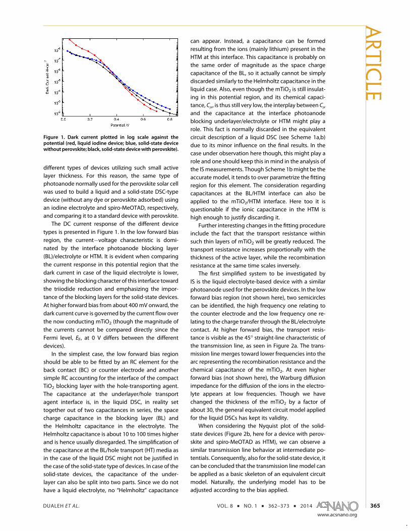
The DC current response of the different devicetypes is presented in Figure 1. In the low forward biasregion, the current�voltage characteristic is domi-nated by the interface photoanode blocking layer(BL)/electrolyte or HTM. It is evident when comparingthe current response in this potential region that thedark current in case of the liquid electrolyte is lower,showing the blocking character of this interface towardthe triiodide reduction and emphasizing the impor-tance of the blocking layers for the solid-state devices.At higher forward bias from about 400mV onward, thedark current curve is governed by the current flow overthe now conducting mTiO2 (though the magnitude ofthe currents cannot be compared directly since theFermi level, EF, at 0 V differs between the differentdevices).
In the simplest case, the low forward bias regionshould be able to be fitted by an RC element for theback contact (BC) or counter electrode and anothersimple RC accounting for the interface of the compactTiO2 blocking layer with the hole-transporting agent.The capacitance at the underlayer/hole transportagent interface is, in the liquid DSC, in reality settogether out of two capacitances in series, the spacecharge capacitance in the blocking layer (BL) andthe Helmholtz capacitance in the electrolyte. TheHelmholtz capacitance is about 10 to 100 times higherand is hence usually disregarded. The simplification ofthe capacitance at the BL/hole transport (HT) media asin the case of the liquid DSC might not be justified inthe case of the solid-state type of devices. In case of thesolid-state devices, the capacitance of the under-layer can also be split into two parts. Since we do nothave a liquid electrolyte, no “Helmholtz” capacitance
can appear. Instead, a capacitance can be formedresulting from the ions (mainly lithium) present in theHTM at this interface. This capacitance is probably onthe same order of magnitude as the space chargecapacitance of the BL, so it actually cannot be simplydiscarded similarly to the Helmholtz capacitance in theliquid case. Also, even though the mTiO2 is still insulat-ing in this potential region, and its chemical capaci-tance, Cμ, is thus still very low, the interplay between Cμand the capacitance at the interface photoanodeblocking underlayer/electrolyte or HTM might play arole. This fact is normally discarded in the equivalentcircuit description of a liquid DSC (see Scheme 1a,b)due to its minor influence on the final results. In thecase under observation here though, this might play arole and one should keep this in mind in the analysis ofthe ISmeasurements. Though Scheme 1bmight be theaccurate model, it tends to over parametrize the fittingregion for this element. The consideration regardingcapacitances at the BL/HTM interface can also beapplied to the mTiO2/HTM interface. Here too it isquestionable if the ionic capacitance in the HTM ishigh enough to justify discarding it.
Further interesting changes in the fitting procedureinclude the fact that the transport resistance withinsuch thin layers of mTiO2 will be greatly reduced. Thetransport resistance increases proportionally with thethickness of the active layer, while the recombinationresistance at the same time scales inversely.
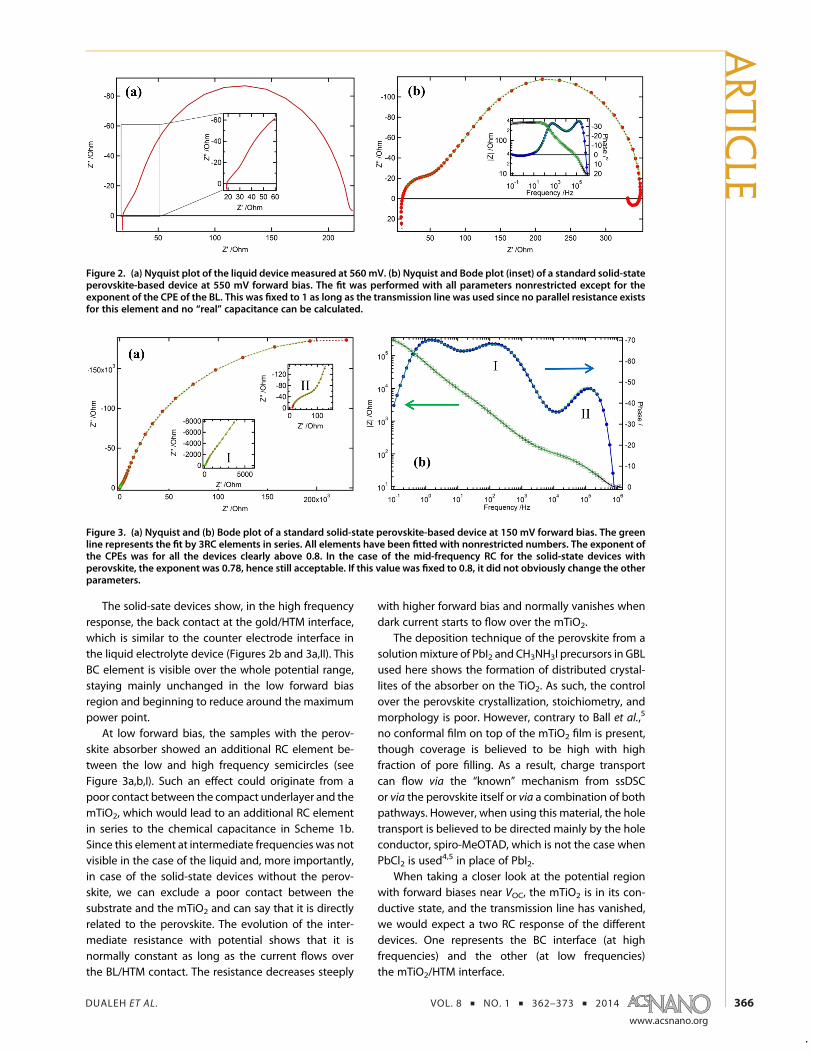
The first simplified system to be investigated byIS is the liquid electrolyte-based device with a similarphotoanode used for the perovskite devices. In the lowforward bias region (not shown here), two semicirclescan be identified, the high frequency one relating tothe counter electrode and the low frequency one re-lating to the charge transfer through the BL/electrolytecontact. At higher forward bias, the transport resis-tance is visible as the 45� straight-line characteristic ofthe transmission line, as seen in Figure 2a. The trans-mission line merges toward lower frequencies into thearc representing the recombination resistance and thechemical capacitance of the mTiO2. At even higherforward bias (not shown here), the Warburg diffusionimpedance for the diffusion of the ions in the electro-lyte appears at low frequencies. Though we havechanged the thickness of the mTiO2 by a factor ofabout 30, the general equivalent circuit model appliedfor the liquid DSCs has kept its validity.
When considering the Nyquist plot of the solid-state devices (Figure 2b, here for a device with perov-skite and spiro-MeOTAD as HTM), we can observe asimilar transmission line behavior at intermediate po-tentials. Consequently, also for the solid-state device, itcan be concluded that the transmission linemodel canbe applied as a basic skeleton of an equivalent circuitmodel. Naturally, the underlying model has to beadjusted according to the bias applied.
Figure 1. Dark current plotted in log scale against thepotential (red, liquid iodine device; blue, solid-state devicewithout perovskite; black, solid-statedevicewith perovskite).
ARTIC
LE
DUALEH ET AL. VOL. 8 ’ NO. 1 ’ 362–373 ’ 2014
www.acsnano.org
366
The solid-sate devices show, in the high frequencyresponse, the back contact at the gold/HTM interface,which is similar to the counter electrode interface inthe liquid electrolyte device (Figures 2b and 3a,II). ThisBC element is visible over the whole potential range,staying mainly unchanged in the low forward biasregion and beginning to reduce around the maximumpower point.
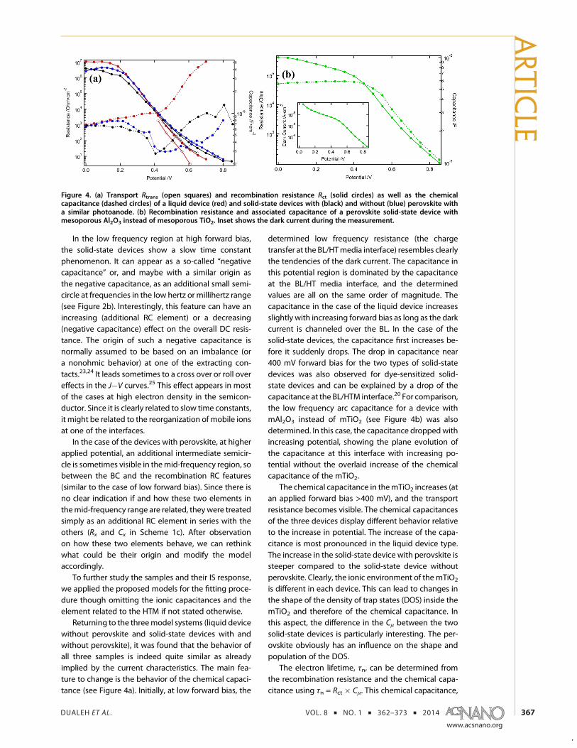
At low forward bias, the samples with the perov-skite absorber showed an additional RC element be-tween the low and high frequency semicircles (seeFigure 3a,b,I). Such an effect could originate from apoor contact between the compact underlayer and themTiO2, which would lead to an additional RC elementin series to the chemical capacitance in Scheme 1b.Since this element at intermediate frequencies was notvisible in the case of the liquid and, more importantly,in case of the solid-state devices without the perov-skite, we can exclude a poor contact between thesubstrate and the mTiO2 and can say that it is directlyrelated to the perovskite. The evolution of the inter-mediate resistance with potential shows that it isnormally constant as long as the current flows overthe BL/HTM contact. The resistance decreases steeply
with higher forward bias and normally vanishes whendark current starts to flow over the mTiO2.
The deposition technique of the perovskite from asolutionmixture of PbI2 and CH3NH3I precursors in GBLused here shows the formation of distributed crystal-lites of the absorber on the TiO2. As such, the controlover the perovskite crystallization, stoichiometry, andmorphology is poor. However, contrary to Ball et al.,5
no conformal film on top of the mTiO2 film is present,though coverage is believed to be high with highfraction of pore filling. As a result, charge transportcan flow via the “known” mechanism from ssDSCor via the perovskite itself or via a combination of bothpathways. However, when using this material, the holetransport is believed to be directed mainly by the holeconductor, spiro-MeOTAD, which is not the case whenPbCl2 is used
4,5 in place of PbI2.When taking a closer look at the potential region
with forward biases near VOC, the mTiO2 is in its con-ductive state, and the transmission line has vanished,we would expect a two RC response of the differentdevices. One represents the BC interface (at highfrequencies) and the other (at low frequencies)the mTiO2/HTM interface.
Figure 2. (a) Nyquist plot of the liquid device measured at 560 mV. (b) Nyquist and Bode plot (inset) of a standard solid-stateperovskite-based device at 550 mV forward bias. The fit was performed with all parameters nonrestricted except for theexponent of the CPE of the BL. This was fixed to 1 as long as the transmission line was used since no parallel resistance existsfor this element and no “real” capacitance can be calculated.
Figure 3. (a) Nyquist and (b) Bode plot of a standard solid-state perovskite-based device at 150 mV forward bias. The greenline represents the fit by 3RC elements in series. All elements have been fitted with nonrestricted numbers. The exponent ofthe CPEs was for all the devices clearly above 0.8. In the case of the mid-frequency RC for the solid-state devices withperovskite, the exponent was 0.78, hence still acceptable. If this value was fixed to 0.8, it did not obviously change the otherparameters.
ARTIC
LE
DUALEH ET AL. VOL. 8 ’ NO. 1 ’ 362–373 ’ 2014
www.acsnano.org
367
In the low frequency region at high forward bias,the solid-state devices show a slow time constantphenomenon. It can appear as a so-called “negativecapacitance” or, and maybe with a similar origin asthe negative capacitance, as an additional small semi-circle at frequencies in the low hertz or millihertz range(see Figure 2b). Interestingly, this feature can have anincreasing (additional RC element) or a decreasing(negative capacitance) effect on the overall DC resis-tance. The origin of such a negative capacitance isnormally assumed to be based on an imbalance (ora nonohmic behavior) at one of the extracting con-tacts.23,24 It leads sometimes to a cross over or roll overeffects in the J�V curves.25 This effect appears in mostof the cases at high electron density in the semicon-ductor. Since it is clearly related to slow time constants,it might be related to the reorganization of mobile ionsat one of the interfaces.
In the case of the devices with perovskite, at higherapplied potential, an additional intermediate semicir-cle is sometimes visible in themid-frequency region, sobetween the BC and the recombination RC features(similar to the case of low forward bias). Since there isno clear indication if and how these two elements inthemid-frequency range are related, they were treatedsimply as an additional RC element in series with theothers (Rx and Cx in Scheme 1c). After observationon how these two elements behave, we can rethinkwhat could be their origin and modify the modelaccordingly.
To further study the samples and their IS response,we applied the proposed models for the fitting proce-dure though omitting the ionic capacitances and theelement related to the HTM if not stated otherwise.
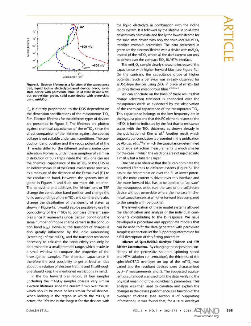
Returning to the threemodel systems (liquid devicewithout perovskite and solid-state devices with andwithout perovskite), it was found that the behavior ofall three samples is indeed quite similar as alreadyimplied by the current characteristics. The main fea-ture to change is the behavior of the chemical capaci-tance (see Figure 4a). Initially, at low forward bias, the
determined low frequency resistance (the chargetransfer at the BL/HTmedia interface) resembles clearlythe tendencies of the dark current. The capacitance inthis potential region is dominated by the capacitanceat the BL/HT media interface, and the determinedvalues are all on the same order of magnitude. Thecapacitance in the case of the liquid device increasesslightly with increasing forward bias as long as the darkcurrent is channeled over the BL. In the case of thesolid-state devices, the capacitance first increases be-fore it suddenly drops. The drop in capacitance near400 mV forward bias for the two types of solid-statedevices was also observed for dye-sensitized solid-state devices and can be explained by a drop of thecapacitance at the BL/HTM interface.20 For comparison,the low frequency arc capacitance for a device withmAl2O3 instead of mTiO2 (see Figure 4b) was alsodetermined. In this case, the capacitance droppedwithincreasing potential, showing the plane evolution ofthe capacitance at this interface with increasing po-tential without the overlaid increase of the chemicalcapacitance of the mTiO2.
The chemical capacitance in themTiO2 increases (atan applied forward bias >400 mV), and the transportresistance becomes visible. The chemical capacitancesof the three devices display different behavior relativeto the increase in potential. The increase of the capa-citance is most pronounced in the liquid device type.The increase in the solid-state device with perovskite issteeper compared to the solid-state device withoutperovskite. Clearly, the ionic environment of themTiO2
is different in each device. This can lead to changes inthe shape of the density of trap states (DOS) inside themTiO2 and therefore of the chemical capacitance. Inthis aspect, the difference in the Cμ between the twosolid-state devices is particularly interesting. The per-ovskite obviously has an influence on the shape andpopulation of the DOS.
The electron lifetime, τn, can be determined fromthe recombination resistance and the chemical capa-citance using τn = Rct � Cμ. This chemical capacitance,
Figure 4. (a) Transport Rtrans (open squares) and recombination resistance Rct (solid circles) as well as the chemicalcapacitance (dashed circles) of a liquid device (red) and solid-state devices with (black) and without (blue) perovskite witha similar photoanode. (b) Recombination resistance and associated capacitance of a perovskite solid-state device withmesoporous Al2O3 instead of mesoporous TiO2. Inset shows the dark current during the measurement.
ARTIC
LE
DUALEH ET AL. VOL. 8 ’ NO. 1 ’ 362–373 ’ 2014
www.acsnano.org
368
Cμ, is directly proportional to the DOS dependent onthe dimension specifications of the mesoporous TiO2
film. Electron lifetimes for the different types of devicesare presented in Figure 5. The lifetimes are plottedagainst chemical capacitance of the mTiO2 since thedirect comparison of the lifetimes against the appliedvoltage is not suitable under such conditions. The con-duction band position and the redox potential of theHT media differ for the different systems under con-sideration. Normally, under the assumption of a similardistribution of bulk traps inside the TiO2, one can usethe chemical capacitance of the mTiO2 or the DOS asan indirectmeasure of the Fermi level ormore preciselyas a measure of the distance of the Fermi level (EF) tothe conduction band. However, the systems investi-gated in Figures 4 and 5 do not meet this criterion.The perovskite and additives like lithium ions or TBPchange the conduction band position and change theionic surroundings of themTiO2 and can therefore alsochange the distribution of the density of states, asshown in Figure 4a. It would also be possible to use theconductivity of the mTiO2 to compare different sam-ples since it represents under certain conditions thesame number of mobile charge carriers in the conduc-tion band (Ecb). However, the transport of charges isalso greatly influenced by the ionic surrounding(screening) of the mTiO2, and the transport resistancenecessary to calculate the conductivity can only bedetermined in a small potential range, which results ina small window to compare the properties of theinvestigated samples. The chemical capacitance istherefore the best possibility to get at least an ideaabout the relation of electron lifetime and EF, althoughone should keep the mentioned restrictions in mind.
In the low forward bias region, all four samples(including the mAl2O3 sample) possess very similarelectron lifetimes since the current flows over the BL,which should be more or less similar for all devices.When looking in the region in which the mTiO2 isactive, the lifetime is the longest for the devices with
the liquid electrolyte in combination with the iodineredox system. It is followed by the lifetime in solid-statedevices with perovskite and finally the lowest lifetime forthe solid-state device with only the spiro-MeOTAD/TiO2
interface (without perovskite). The data presented ingreen are the electron lifetimewith a devicewithmAl2O3
instead of the mTiO2 where all the dark current can onlybe driven over the compact TiO2 BL/HTM interface.
ThemAl2O3 sample clearly shows no increase of thecapacitance with higher forward bias (see Figure 4b).On the contrary, the capacitance drops at higherpotential. Such a behavior was already observed forssDSC-type devices using ZrO2 in place of mTiO2 bututilizing thicker mesoporous films.20,23,24
We can conclude on the basis of these results thatcharge (electron) transport is channeled over themesoporous oxide as evidenced by the observationof the chemical capacitance of the mesoporous TiO2.This capacitance belongs to the low frequency arc inthe Nyquist plot and that this RC element relates to themTiO2 is further indicated by the fact that its resistancescales with the TiO2 thickness as shown already inthe publication of Kim et al.3 Another result whichsupports our conclusion is presented in the publicationbyAbrusci et al.26 inwhich the capacitance determinedby charge extraction measurements is much smallerfor the case in which the electrons are not injected intoa mTiO2 but a fullerene layer.
One can also observe that the BL can dominate theobserved lifetimes to different extents (Figure 5). Theeasier the recombination over the BL at lower poten-tial, the more current is driven over this interface andthe more forward bias has to be applied to “activate”the mesoporous oxide (see the case of the solid-statedevice without perovskite where the increase in che-mical capacitance is at a higher forward bias comparedto the sample with perovskite).
The investigation of these model systems allowedthe identification and analysis of the individual com-ponents contributing to the IS response. We havedeveloped a procedure and appropriate models thatcan be used to fit the data generated with perovskitesamples; see section I of the Supporting Information fora full description of this fitting procedure.
Influence of Spiro-MeOTAD Overlayer Thickness and HTMAdditive Concentrations. By changing the deposition con-ditions of the perovskite solution (spinning speedand HTM solution concentration), the thickness of thespiro-MeOTAD overlayer on top of the mTiO2 wasvaried and the resultant devices were characterizedby J�V measurements and IS. The suggested equiva-lent circuit model was used to fit the data, verifying thephysical meaning of the individual IS parameters. Thisanalysis was then used to correlate and explain thechanges in the device performance as a function of theoverlayer thickness (see section II of SupportingInformation). It was found that, for a HTM overlayer
Figure 5. Electron lifetime as a function of the capacitance(red, liquid iodine electrolyte-based device; black, solid-state device with perovskite; blue, solid-state device with-out perovskite; green, solid-state device with perovskiteusing mAl2O3).
ARTIC
LE

DUALEH ET AL. VOL. 8 ’ NO. 1 ’ 362–373 ’ 2014
www.acsnano.org
369
thickness between 0 and 136 nm, the HTM forms aconformal overlayer, blocking the direct contact be-tween the perovskite and the gold back contact, thusleading to an increase in the VOC and the JSC of solarcells. In our previous work,20 the charge transportresistance of the spiro-MeOTADwas shown tomanifestas an RC arc at high to intermediate frequencies in theNyquist plots. For thin HTM overlayers up to 140 nm,the magnitude of the high frequency resistance issimilar and hence attributed to the charge transportresistance at the back contact (BC)/HTM interface, asthe transport resistance of the HTM is too small to beresolved for such thin overlayers. As the HTM over-layer is increased above 136 nm, the increase in seriesresistance arising from the increasingly large chargetransport resistance values of the spiro-MeOTAD(Figure 6) leads to a decrease in the fill factor (FF) andthus in the overall cell power conversion efficiency(PCE), reflected in the drop in JSC and VOC.
Furthermore, the influence of the common addi-tives to the HTM solution, LiTFSI and TBP, on the ISparameters was investigated (see sections III and IV ofSupporting Information). These displayed similar ef-fects as already known from the study of ssDSCs andliquid DSCs, confirming the validity of the IS equivalentcircuit applied to the analysis here. In the case of LiTFSI,the role of lithium ions is rather complex, where thepresence of Liþ is known to influence the dopingmechanism of the spiro-MeOTAD27,28 as well as themobility of charges. Deviceswithout any LiTFSI contentdisplayed an additional resistive element (see Support-ing Information Figure S12) that ismost likely related tothe transport resistance in theHTM. Liþ also plays a rolein the screening of the negative charge of the electronsinside the mTiO2 enabling a facilitated charge trans-port,29 and the lithium ions were observed to induce ashift of the conduction band of the mTiO2 to lowervoltage. The increasing content of the Liþ ions more-over was found to influence the shape of the DOS andincrease the lifetime of the electrons.
In the case of TBP, it was found that it acts as arecombination blocking agent, hence increasing therecombination resistance for the electrons at high TBPcontent. Additionally, as in the case of conventionalDSCs,30�34 the TBP leads to an upward shift in theconduction band edge of themTiO2, which is observedin the chemical capacitance (see Supporting Informa-tion Figure S18). This directly influences the VOC of thedevices, leading to an increase inVOC as the conductionband is shifted upward with increasing TBP concentra-tion. The increase in concentration of TBP also results inan increase of the series resistance, leading to lower FFof devices. Pyridine compounds such as TBP are knownto adsorb onto gold electrodes35 and therefore act as ablocking layer for the charge transfer at the interfacebetween the gold and the HTM. Furthermore, thehigh binding strength of TBP results in a decreased
concentration of “free” Li ions, leading additionally toan increasing of the series resistance as the transportresistance of the HTM becomes larger as the spiro-MeOTAD is less p-doped.
Standard Devices under Illumination. So far, the deviceswere only investigated under dark conditions. Theimpedance measurements revealed that most of thebasic concepts from related devices like DSCs andssDSCs keep their validity. However, differences alsoappear such as the additional semicircle at intermedi-ate frequencies and, for example, the behavior of JSCand VOC with increasing HTM overlayer.
There exists a strong hysteresis in the J�V curvesunder illumination (see section V in Supporting Infor-mation Figure S20), which manifests mainly only in theforward scan (from low to high forward bias). Such aneffect is not detectable in the dark measurements. ThePCE values for the different scan velocities can be seenin Table 1. The backward scan fromhigh to low forwardbias showed nearly no dependence on scan velocity.On the other hand, the efficiency of the forward scanfrom low to high forward bias is strongly velocity-dependent, indicating that some slow charged carriersare involved in the current and voltage generation.
In the transient photocurrent dynamics, slow reac-tion times of the perovskite devices can similarlybe observed (Supporting Information Figure S21).
Figure 6. Magnitude of the high frequency resistance de-terminedat a correctedpotential of 0.2 V as a functionof theHTM overlayer thickness.
TABLE 1. PCE Values for a Device Scanned with Different
Velocitiesa
scan velocity (mV s�1) JSC (mA cm�2) VOC (V) FF efficiency (%)
200 B 16.07 0.85 0.72 9.69200 F 16.07 0.83 0.54 7.19100 B 15.74 0.84 0.72 9.50100 F 15.67 0.84 0.58 7.6250 B 15.35 0.84 0.72 9.3050 F 15.30 0.84 0.62 7.9010 B 14.80 0.84 0.72 8.9410 F 14.78 0.84 0.67 8.33
a Here from VOC to 0 V and back, F = 0 V to VOC (forward scan), B = VOC to 0 V(backward scan).
ARTIC
LE

DUALEH ET AL. VOL. 8 ’ NO. 1 ’ 362–373 ’ 2014
www.acsnano.org
370
The current dynamics show first a steep rise of thecurrent after the red light LED pulse, which decays fast.After this initial fast decay, a slow rise of the photo-current can be observed. After the red light pulse isstopped, a fast decay of the photocurrent is followedby a slow decay. A similar observation can be seen forthe photovoltage rise and decay after the light pulse.The fitting procedure included two exponentials, oneused to fit the fast rise and decay and the otherexponential for the slow component. The time con-stant for the slow component of the photocurrentyields a time constant of about 16 ms for the riseand 15 ms for the decay. The time constant associatedwith the photovoltage rise and decay is 32 and 26 ms,respectively.
Such an effect should manifest in the IS measure-ments, and indeed, a slow time constant phenomenacan be observed under illumination (Figure 7).
This poses the question of the origin of this slowprocess, which clearly has an influence on the PCE ofsuch devices. There are several possibilities for such aneffect, mainly ionic charge transport, ion intercalation,or it might even be a ferroelectric effect. Generally, it isclear that this feature is mainly a light-induced effect,as it does not appear to the same extent for measure-ments conducted under dark conditions. To furtherexamine this process, a perovskite device without HTMwas built and measured under illumination to verify ifsuch a slow phenomenon is still observable. Indeed,such a phenomena can be detected in the IS response.Hence, this excludes a photointercalation phenomen-on as a possible origin. As described above, we couldobserve an additional resistive element under darkconditions at low forward bias attributed to a chargetransport through the perovskite. This feature wasobserved to vanish under illumination. This shows thatthe ability of this perovskite interfacial layer to trans-port charges is strongly increased under illumination.The electronic conductivity of the perovskite layer willbe high under illumination, but some charge carriersseem to be transported by ions. Furthermore, wecannot fully exclude other possible contributions likethe previously mentioned ferroelectric effect.36
Apart from the slow component in the Nyquist plot,two different elements can be observed under illumi-nation: the high frequency RC for the BC/HTM interfaceand the element associated with the chemical capaci-tance and the recombination resistance of the mTiO2.At lower light intensities, a third element, a transmis-sion line for the transport inside the TiO2, is also visible.
The J�V characteristic and a comparison of the ISfitting results in the dark and under illumination can beseen in Figure 8a,b, respectively. One can clearly ob-serve the similar behavior of the increasing chemicalcapacitance at high forward bias in the dark and underillumination, while the recombination resistance aswell as the transport resistance for the electrons is
greatly reduced when under illumination. The chargecollection efficiency, ηcc, which can be calculatedaccording to ηcc = 1/(1 þ (τtrans/τn,)), shows about80�85% (see Supporting Information Figure S22). Asalready observed in the relationship between thetransport and recombination resistance in the dark(see Figure 8b), the charge collection efficiency is oneof the critical parameters for reaching high photocur-rent in such devices. As visible at 40% light intensity,the charge collection efficiency is considerably lowerthan in the case of a typical liquid DSC, which isgenerally over 95% also at full sunlight intensity.Increasing to 100% light intensity for such perovskitedevices leads to further reduction in ηcc to below 80%.This shows that by the applied fitting procedure oneidentifies a key parameter which has to be furtheroptimized in such devices, the charge collection effi-ciency. As clearly found in this investigation, the JSC canstill be improved in this type of devices when, forexample, reducing the recombination while maintain-ing a similar transport resistance. This would lead to anincreased JSC and VOC and finally to an overall increaseddevice efficiency.
Final Statements. As mentioned above, the IS re-sponse associated with the perovskite at intermediatefrequencies needs to be addressed. We believe thatthere is injection of charge carriers from and to theperovskite with the TiO2. This could be clearly shownby the change of the capacitance associated with therecombination arc generating the current (Figure 4)and in the publications of Abrusci et al.26 WithoutmTiO2, no real increase in the capacitance is visible(with the simplification mentioned for the fitting pro-cedure from Scheme 1b to 1c), showing that thecapacitance can be used as a clear indicator for theactive part of the mTiO2 in the charge transfer pro-cesses. The origin of the RC element at intermediatefrequencies at low forward bias in the dark is, as alreadymentioned above, most probably related to the per-ovskite. This element is quite insensitive to any of thetreatments presented here except for the case of thelow TBP content. This is explained by the indirect effect
Figure 7. Nyquist plot of a standard device under illumina-tion at 0 V. Inset shows the frequencies from the MHz downto about 10 Hz.
ARTIC
LE

DUALEH ET AL. VOL. 8 ’ NO. 1 ’ 362–373 ’ 2014
www.acsnano.org
371
of the TBP binding with the Liþ ions decreasing theconcentration of “free” Liþ ions, thus leading to anincrease in the transport resistance of the perovskiteand the HTM. As we believe that there is a relativelyconformal film of the perovskite on top of the BL andon the mTiO2, charges have to be channeled via thisperovskite film. As such, it acts like an intermediatelayer between the mTiO2 and the HTM. This is furthervalidated by the disappearance of this feature whenthe devices are under illumination and the perovskite isvery conductive.
CONCLUSIONS
In this work, solid-state mesoscopic solar cells usinglead-iodide-based perovskite deposited onto sub-micrometer thick mesoporous TiO2 in combinationwith spiro-MeOTAD as a HTM are investigated usingIS. Through comparison with the well-known liquidand solid-state DSC systems, these devices are ana-lyzed and interpreted, systematically establishing anequivalent circuit model that can be applied to the ISanalysis of this type of devices. This model is thenemployed to explore the effect of the concentrationvariation of the common HTM solution additives, TBP
and LiTFSI, on the device parameter. Additionally, theinfluence of the overlayer thickness of the HTM on topof the mTiO2 is investigated. From these experiments,the working mechanism of these perovskite devices isexplored and the presented model used for the ISinterpretation is validated. The complex nature of thissystem is exposed, and the interplay of various compo-nents (i.e., additive ratios) is highlighted. The experimen-tal results show the multiple roles and effects of the Liþ
ion and TBP concentrations in the HTM on the internalelectrical parameters and consequently on the overalldevice performance.The model presented further identifies the separate
features corresponding to the electronic and presum-ably ionic conductivities of the lead-iodide-based per-ovskitematerial. These features are unique to this systemand are believed to greatly depend on the morphologyand nature of the perovskite material as these define itstransport and electrical properties. As such, this investi-gation shows that IS is a useful tool for characterizing thistype of system, and the developed IS model can beapplied to examine the perovskite material in workingdevice configurations to identify the limiting processesreducing the overall efficiency of the solar cells.
METHODS
Materials. All chemicals were purchased from Sigma-Aldrichand used as received. 2,20 ,7,70-Tetrakis(N,N-di-p-methoxy-phenylamine)-9,90-spirobifluorene (spiro-MeOTAD) was pur-chased from Merck and used as received. The CH3NH3I pre-zcursor was synthesized in our laboratory.
Device Fabrication. Fluorine-doped tin oxide (FTO)-coatedglass substrates (TEC 15, Pilkington) were patterned by laseretching to give the desired electrode configuration. Afterundergoing thorough cleaning by mechanical scrubbing usingHellmanex, ultrasonication, and finally ozone cleaning, a TiO2
compact layer was deposited on the substrates by spraypyrolysis at 450 �C using the precursor titanium diisopropoxidebis(acetylacetonate) diluted in ethanol (1:10 volume ratio) andoxygen as the carrier gas. The substrates were subsequentlyimmersed in a 0.02 M aqueous solution of TiCl4 for 30 min at70 �C, after which they were rinsed with water and heated at500 �C for 20 min. The sub-micrometer mesoporous TiO2 layer
was deposited by spin-coating TiO2 paste (Dyesol 18NR-T)diluted in ethanol at 1:2.5 by weight at 2000 rpm. The filmswere heated stepwise to 500 �C at which they were sintered for15 min. While still hot, the substrates were transferred into adrybox. All subsequent deposition steps were carried out underdry conditions. The perovskite precursor solution was preparedas reported by Kim et al.3 A 1:1 molar ratio mixture of PbI3 andCH3NH3I was dissolved in γ-butyrolactone (GBL) at 30 wt % byheating at 60 �C overnight. This solutionwas deposited onto themTiO2 films by spin-coating at 2000 rpm for 30 s. The films werethen annealed at 100 �C for 5�10 min and cooled to roomtemperature. The color of the films was observed to changefrom yellow to dark brown. The standard hole transportmaterialsolution was prepared by dissolving 0.059 M spiro-MeOTAD inchlorobenzene, to which 1% molar ratio of cobalt(III) dopant,0.05 M tert-butylpyridine (TBP), and 0.009 M Li[(CF3SO2)2N](LiTFSI) were added. Both the cobalt(III) complex, tris(2-(1H-pyrazol-1-yl)-4-tert-butylpyridine)cobalt(III)-tris(bis(trifluoro-methylsulfonyl)imide)), coded FK209, and the LiTFSI salt were
Figure 8. (a) Current�voltage characteristic in the dark (black) and under illumination at 40% sun light intensity by LED (red).(b) Extracted impedance result of the recombination resistance (solid circles), the transport resistance (open squares), and thechemical capacitance (dashed triangles).
ARTIC
LE
DUALEH ET AL. VOL. 8 ’ NO. 1 ’ 362–373 ’ 2014
www.acsnano.org
372
predissolved in acetonitrile. The HTM solution was deposited onthe perovskite-sensitized films by spin-coating at 4000 rpm for30 s unless specified otherwise. The devices were completed bythermal evaporation of 60 nmof Au counter electrode. Cells werenot sealed but stored in the dark under dry conditions. Thecounter electrode of the liquid DSCwas a thermally deposited Pt.The counter electrode was attached to the substrate with themTiO2 by a hot melt polymer. The electrolyte injected beforesealing the device is coded Z952.
Impedance Measurements. The impedance measurementswere performed using a Bio-Logic SP300 potentiostat. A dc po-tential bias was applied and overlaid by a sinusoidal ac potentialperturbation of 15mVover a frequency range of 7MHz to 0.1 Hz(for themeasurements under illumination, the lowest frequencyis 0.01 Hz). The applied dc potential bias was changed by∼50 mV steps from 850 to 0 mV. The resulting impedancespectra were fitted using the ZView software (Scribner Associ-ates Inc.).
Transient Measurements. The transient photovoltage andphotocurrent measurement setup is similar to the descriptionby O'Regan et al.37,38 White bias light was provided by an arrayof diodes (Lumiled model LXHL-NWE8 white star). For the smallperturbation, red-light-pulsed diodes (LXHLND98 redstar,0.2 s square pulse width, 100 ns rise and fall time) were used,controlled by a fast solid-state switch. The voltage dynamicswere recorded via a Keithley 2602 sourcemeter. The voltagedecay measurements were performed from zero current (VOC).Small perturbation transient photocurrent measurements wereperformed in a similar way to the open-circuit voltage decaymeasurements but here holding a fixed potential whilemeasur-ing the photocurrent transients. The decays were fitted with adouble exponential decay.
Conflict of Interest: The authors declare no competingfinancial interest.
Acknowledgment. We acknowledge financial support fromAisin Cosmos R&D Co., Ltd., Japan, and from the EuropeanCommunity's Seventh Framework Programme (FP7/2007-2013)under the “ORION” Grant Agreement No. NMP-229036. M.G.thanks the European Research Council for an Advanced Re-search Grant ARG 247404 funded under the “Mesolight” project.M.K.N. thanks the World Class University programs (PhotovoltaicMaterials, Department of Material Chemistry, Korea University),funded by the Ministry of Education, Science and Technologythrough the National Research Foundation of Korea (R31-2008-000-10035-0).
Supporting Information Available: IS fitting procedure, tran-sient current and photovoltage dynamics, J�V characteristic ata scan velocity of 100 mV/s, recombination resistance, capaci-tance and dark current measurement of perovskite solid-statedevice using mesoporous Al2O3 in place of mTiO2, chargecollection efficiency of standard perovskite solid-state deviceunder 40% sun intensity, experimental data and additionaldiscussion on variation of TBP and LiTFSI additive concentra-tions andHTMoverlayer thickness. Thismaterial is available freeof charge via the Internet at http://pubs.acs.org.
REFERENCES AND NOTES1. Im, J.-H.; Lee, C.-R.; Lee, J.-W.; Park, S.-W.; Park, N.-G. 6.5%
Efficient Perovskite Quantum-Dot-Sensitized Solar Cell.Nanoscale 2011, 3, 4088–4093.
2. Chung, I.; Lee, B.; He, J.; Chang, R. P. H.; Kanatzidis, M. G. All-Solid-State Dye-Sensitized Solar Cells with High Efficiency.Nature 2012, 485, 486–489.
3. Kim, H.-S.; Lee, C.-R.; Im, J.-H.; Lee, K.-B.; Moehl, T.; Marchioro,A.; Moon, S.-J.; Humphry-Baker, R.; Yum, J.-H.; Moser, J.-E.;et al. Lead Iodide Perovskite Sensitized All-Solid-State Sub-micron Thin Film Mesoscopic Solar Cell with EfficiencyExceeding 9%. Sci. Rep. 2012, 2, 591.
4. Lee, M. M.; Teuscher, J.; Miyasaka, T.; Murakami, T. N.;Snaith, H. Efficient Hybrid Solar Cells Based on Meso-Superstructured Organometal Halide Perovskites. Science2012, 338, 643–647.
5. Ball, J. M.; Lee, M. M.; Hey, A.; Snaith, H. Low-TemperatureProcessed Meso-Superstructured to Thin-Film PerovskiteSolar Cells. Energy Environ. Sci. 2013, 6, 1739–1743.
6. Etgar, L.; Gao, P.; Xue, Z.; Peng, Q.; Chandiran, A. K.; Liu, B.;Nazeeruddin, M. K.; Grätzel, M. Mesoscopic CH3NH3PbI3/TiO2
Heterojunction Solar Cells. J. Am. Chem. Soc. 2013, 134,17396–17399.
7. Misusaki, J.; Arai, K.; Fueki, K. Ionic Conduction ofthe Perovskite-Type Halides. Solid State Ionics 1983, 11,203–211.
8. Inaguma, Y.; Liquan, C.; Itoh, M.; Nakamura, T.; Uchida, T.;Ikuta, H.; Wakihara, M. High Ionic Conductivity in LithiumLanthanum Titanate. Solid State Commun. 1993, 86, 689–693.
9. Mitzi, D. B. Solution-Processed Inorganic Semiconductors.J. Mater. Chem. 2004, 14, 2355–2365.
10. Kagan, C.; Mitzi, D.; Dimitrakopoulos, C. Organic�InorganicHybrid Materials as Semiconducting Channels in Thin-FilmField-Effect Transistors. Science 1999, 286, 945–947.
11. Billing, D. G.; Lemmerer, A. Inorganic�Organic HybridMaterials Incorporating Primary Cyclic AmmoniumCations: The Lead Iodide Series. CrystEngComm 2007, 9,236–244.
12. Mitzi, D. B.; Chondroudis, K.; Kagan, C. R. Design, Structure,and Optical Properties of Organic-Inorganic PerovskitesContaining an Oligothiophene Chromophore. Inorg.Chem. 1999, 38, 6246–6256.
13. Fluegel, B.; Zhang, Y.; Mascarenhas, A.; Huang, X.; Li, J.Electronic Properties of Hybrid Organic�Inorganic Semi-conductors. Phys. Rev. B 2004, 70, 205308.
14. Mitzi, D. B.; Feild, C. A.; Harrison, W. T. A.; Guloy, A. M.Conducting Tin Halides with a Layered Organic-BasedPerovskite Structure. Nature 1994, 369, 467–469.
15. Chang, Y. H.; Park, C. H.; Matsuishi, K. First-PrinciplesStudy of the Structural and the Electronic Properties ofthe Lead-Halide-Based Inorganic�Organic Perovskites(CH3NH3)PbX3 And CsPbX3 (X = Cl, Br, I). J. Korean Phys.Soc. 2004, 44, 889–893.
16. Noh, J. H.; Im, S. H.; Heo, J. H.; Mandal, T. N.; Seok, S. I.Chemical Management for Colorful, Efficient, and StableInorganic�Organic Hybrid Nanostructured Solar Cells.Nano Lett. 2013, 13, 1764–1769.
17. Bi, D.; Yang, L.; Boschloo, G.; Hagfeldt, A.; Johansson, E. M. J.Effect of Different Hole Transport Materials on Recombi-nation in CH3NH3PbI3 Perovskite-Sensitized MesoscopicSolar Cells. J. Phys. Chem. Lett. 2013, 4, 1532–1536.
18. Heo, J. H.; Im, S. H.; Noh, J. H.; Mandal, T. N.; Lim, C.-S.;Chang, J. A.; Lee, Y. H.; Kim, H.-J.; Sarkar, A.; Nazeeruddin,M. K.; et al. Efficient Inorganic�Organic Hybrid Hetero-junction Solar Cells Containing Perovskite Compoundand Polymeric Hole Conductors. Nat. Photonics 2013, 7,486–491.
19. Edri, E.; Kirmayer, S.; Cahen, D.; Hodes, G. HighOpen-CircuitVoltage Solar Cells Based on Organic�Inorganic LeadBromide Perovskite. J. Phys. Chem. Lett. 2013, 4, 897–902.
20. Dualeh, A.; Moehl, T.; Nazeeruddin, M. K.; Grätzel, M.Temperature Dependence of Transport Properties ofSpiro-MeOTAD as a Hole Transport Material in Solid-StateDye-Sensitized Solar Cells. ACS Nano 2013, 7, 2292–2301.
21. Boix, P. P.; Larramona, G.; Jacob, A.; Delatouche, B.; Mora-Sero, I.; Bisquert, J. Hole Transport and Recombination inAll-Solid Sb2S3-Sensitized TiO2 Solar Cells Using CuSCN asHole Transporter. J. Phys. Chem. C 2012, 116, 1579–1587.
22. Kim, H.-S.; Mora-Sero, I.; Gonzalez-Pedro, V.; Fabregat-Santiago, F.; Juarez-Perez, E. J.; Park, N.-G.; Bisquert, J.Mechanism of Carrier Accumulation in Perovskite Thin-Absorber Solar Cells. Nat. Commun. 2013, 4, 2242.
23. Bisquert, J. A Variable Series Resistance Mechanism ToExplain the Negative Capacitance Observed in ImpedanceSpectroscopy Measurements of Nanostructured SolarCells. Phys. Chem. Chem. Phys. 2011, 13, 4679–4685.
24. Mora-Sero, I.; Bisquert, J.; Fabregat-Santiago, F.; Garcia-Belmonte, G.; Zoppi, G.; Durose, K.; Proskuryakov, Y.; Oja, I.;Belaidi, A.; Dittrich, T.; et al. Implications of the NegativeCapacitance Observed at Forward Bias in Nanocomposite
ARTIC
LE

DUALEH ET AL. VOL. 8 ’ NO. 1 ’ 362–373 ’ 2014
www.acsnano.org
373
and Polycrystalline Solar Cells. Nano Lett. 2006, 6,640–650.
25. Eisenbarth, T.; Caballero, R.; Nichterwitz, M.; Kaufmann,C. A.; Schock, H.-W.; Unold, T. Characterization of Metast-abilities in Cu(In,Ga)Se2 Thin-FilmSolar Cells byCapacitanceand Current�Voltage Spectroscopy. J. Appl. Phys. 2011,110, 094506-13.
26. Abrusci, A.; Stranks, S. D.; Docampo, P.; Yip, H.-L.; Jen, A.-K.Y.; Snaith, H. High-Performance Perovskite-Polymer Hy-brid Solar Cells via Electronic Coupling with FullereneMonolayers. Nano Lett. 2013, 13, 3124–3128.
27. Abate, A.; Leijtens, T.; Pathak, S.; Teuscher, J.; Avolio, R.;Errico, M. E.; Kirkpatrik, J.; Ball, J. M.; Docampo, P.; McPherson,I.; et al. Lithium Salts as “Redox Active” p-Type Dopants forOrganic Semiconductors and Their Impact in Solid-StateDye-Sensitized Solar Cells. Phys. Chem. Chem. Phys. 2013,15, 2572–2579.
28. Snaith, H.; Grätzel, M. Enhanced Charge Mobility in aMolecular Hole Transporter via Addition of Redox InactiveIonic Dopant: Implication to Dye-Sensitized Solar Cells.Appl. Phys. Lett. 2006, 89, 262114-3.
29. Kambe, S.; Nakade, S.; Kitamura, T.; Wada, Y.; Yanagida, S.Influence of the Electrolytes on Electron Transport inMesoporous TiO2�Electrolyte Systems. J. Phys. Chem. B2002, 106, 2967–2972.
30. Koops, S. E.; O'Regan, B.; Barnes, P. R. F.; Durrant, J. R.Parameters Influencing the Efficiency of Electron Injectionin Dye-Sensitized Solar Cells. J. Am. Chem. Soc. 2009, 131,4808–4818.
31. Katoh, R.; Kasuya, M.; Kodate, S.; Furube, A.; Fuke, N.; Koide,N. Effects of 4-tert-Butylpyridine and Li Ions on Photo-induced Electron Injection Efficiency in Black-Dye-Sensi-tized Nanocrystalline TiO2 Films. J. Phys. Chem. C 2011,113, 20738–20744.
32. Howie, W. H.; Harris, J. E.; Jennings, J. R.; Peter, L. M. Solid-State Dye-Sensitized Solar Cells Based on Spiro-MeOTAD.Sol. Energy Mater. Sol. Cells 2007, 91, 424–426.
33. Dürr, M.; Rosselli, S.; Yasuda, A.; Nelles, G. Band-GapEngineering of Metal Oxides for Dye-Sensitized Solar Cells.J. Phys. Chem. B 2006, 110, 21899–21902.
34. Zhao, Y.; Chen, W.; Zhai, J.; Sheng, X.; He, Q.; Wei, T.; Bai, F.;Jiang, L.; Zhu, D. Solid-State Dye-Sensitized PhotovoltaicDevice with Newly Designed Small Organic Molecule asHole-Conductor. Chem. Phys. Lett. 2007, 445, 259–264.
35. Jurkiewicz-Herbich,M.; Slojkowska, R.; Zawada,K.; Bukowska, J.Electrochemical and Surface-Enhanced Raman SpectroscopyStudies of 4-Phenylpyridine Adsorption at the Gold/SolutionInterface. Electrochim. Acta 2002, 47, 2429–2434.
36. Stoumpos, C. C.; Malliakas, C. D.; Kanatzidis, M. G. Semi-conducting Tin and Lead Iodide Perovskites with OrganicCations: Phase Transitions, High Mobilities, and Near-Infrared Photoluminescent Properties. Inorg. Chem.2013, 15, 9019–9038.
37. O' Regan, B. C.; Lenzmann, F. Charge Transport andRecombination in a Nanoscale Interpenetrating Networkof n-Type and p-Type Semiconductors: Transient Photo-current and Photovoltage Studies of TiO2/Dye/CuSCNPhotovoltaic Cells. J. Phys. Chem. B 2004, 108, 4342–4350.
38. O'Regan, B. C.; Bakker, K.; Kroeze, J.; Smit, H.; Sommeling, P.;Durrant, J. R. Measuring Charge Transport from TransientPhotovoltage Rise Times. A New Tool To InvestigateElectron Transport in Nanoparticle Films. J. Phys. Chem. B2006, 110, 17155–17160.
ARTIC
LE

本文献由“学霸图书馆-文献云下载”收集自网络,仅供学习交流使用。
学霸图书馆(www.xuebalib.com)是一个“整合众多图书馆数据库资源,
提供一站式文献检索和下载服务”的24 小时在线不限IP
图书馆。
图书馆致力于便利、促进学习与科研,提供最强文献下载服务。
图书馆导航:
图书馆首页 文献云下载 图书馆入口 外文数据库大全 疑难文献辅助工具


![Fluorinated 2D Lead Iodide Perovskite Ferroelectrics€¦ · characterization of piezoresponse force microscopy (PFM) was carried out.[15] Since the as-grown crystal is in monodomain](https://img.dokumen.tips/doc/110x75/60fa64a0a39b09301307d15a/fluorinated-2d-lead-iodide-perovskite-ferroelectrics-characterization-of-piezoresponse.jpg)