Embed Size (px)
Citation preview

Advanced Design System 2011.01 - Impedance Matching Utility
1
Advanced Design System 2011.01
Feburary 2011Impedance Matching Utility

Advanced Design System 2011.01 - Impedance Matching Utility
2
© Agilent Technologies, Inc. 2000-20115301 Stevens Creek Blvd., Santa Clara, CA 95052 USANo part of this documentation may be reproduced in any form or by any means (includingelectronic storage and retrieval or translation into a foreign language) without prioragreement and written consent from Agilent Technologies, Inc. as governed by UnitedStates and international copyright laws.
AcknowledgmentsMentor Graphics is a trademark of Mentor Graphics Corporation in the U.S. and othercountries. Mentor products and processes are registered trademarks of Mentor GraphicsCorporation. * Calibre is a trademark of Mentor Graphics Corporation in the US and othercountries. "Microsoft®, Windows®, MS Windows®, Windows NT®, Windows 2000® andWindows Internet Explorer® are U.S. registered trademarks of Microsoft Corporation.Pentium® is a U.S. registered trademark of Intel Corporation. PostScript® and Acrobat®are trademarks of Adobe Systems Incorporated. UNIX® is a registered trademark of theOpen Group. Oracle and Java and registered trademarks of Oracle and/or its affiliates.Other names may be trademarks of their respective owners. SystemC® is a registeredtrademark of Open SystemC Initiative, Inc. in the United States and other countries and isused with permission. MATLAB® is a U.S. registered trademark of The Math Works, Inc..HiSIM2 source code, and all copyrights, trade secrets or other intellectual property rightsin and to the source code in its entirety, is owned by Hiroshima University and STARC.FLEXlm is a trademark of Globetrotter Software, Incorporated. Layout Boolean Engine byKlaas Holwerda, v1.7 http://www.xs4all.nl/~kholwerd/bool.html . FreeType Project,Copyright (c) 1996-1999 by David Turner, Robert Wilhelm, and Werner Lemberg.QuestAgent search engine (c) 2000-2002, JObjects. Motif is a trademark of the OpenSoftware Foundation. Netscape is a trademark of Netscape Communications Corporation.Netscape Portable Runtime (NSPR), Copyright (c) 1998-2003 The Mozilla Organization. Acopy of the Mozilla Public License is at http://www.mozilla.org/MPL/ . FFTW, The FastestFourier Transform in the West, Copyright (c) 1997-1999 Massachusetts Institute ofTechnology. All rights reserved.
The following third-party libraries are used by the NlogN Momentum solver:
"This program includes Metis 4.0, Copyright © 1998, Regents of the University ofMinnesota", http://www.cs.umn.edu/~metis , METIS was written by George Karypis([email protected]).
Intel@ Math Kernel Library, http://www.intel.com/software/products/mkl
SuperLU_MT version 2.0 - Copyright © 2003, The Regents of the University of California,through Lawrence Berkeley National Laboratory (subject to receipt of any requiredapprovals from U.S. Dept. of Energy). All rights reserved. SuperLU Disclaimer: THISSOFTWARE IS PROVIDED BY THE COPYRIGHT HOLDERS AND CONTRIBUTORS "AS IS"AND ANY EXPRESS OR IMPLIED WARRANTIES, INCLUDING, BUT NOT LIMITED TO, THEIMPLIED WARRANTIES OF MERCHANTABILITY AND FITNESS FOR A PARTICULAR PURPOSEARE DISCLAIMED. IN NO EVENT SHALL THE COPYRIGHT OWNER OR CONTRIBUTORS BELIABLE FOR ANY DIRECT, INDIRECT, INCIDENTAL, SPECIAL, EXEMPLARY, ORCONSEQUENTIAL DAMAGES (INCLUDING, BUT NOT LIMITED TO, PROCUREMENT OF

Advanced Design System 2011.01 - Impedance Matching Utility
3
SUBSTITUTE GOODS OR SERVICES; LOSS OF USE, DATA, OR PROFITS; OR BUSINESSINTERRUPTION) HOWEVER CAUSED AND ON ANY THEORY OF LIABILITY, WHETHER INCONTRACT, STRICT LIABILITY, OR TORT (INCLUDING NEGLIGENCE OR OTHERWISE)ARISING IN ANY WAY OUT OF THE USE OF THIS SOFTWARE, EVEN IF ADVISED OF THEPOSSIBILITY OF SUCH DAMAGE.
7-zip - 7-Zip Copyright: Copyright (C) 1999-2009 Igor Pavlov. Licenses for files are:7z.dll: GNU LGPL + unRAR restriction, All other files: GNU LGPL. 7-zip License: This libraryis free software; you can redistribute it and/or modify it under the terms of the GNULesser General Public License as published by the Free Software Foundation; eitherversion 2.1 of the License, or (at your option) any later version. This library is distributedin the hope that it will be useful,but WITHOUT ANY WARRANTY; without even the impliedwarranty of MERCHANTABILITY or FITNESS FOR A PARTICULAR PURPOSE. See the GNULesser General Public License for more details. You should have received a copy of theGNU Lesser General Public License along with this library; if not, write to the FreeSoftware Foundation, Inc., 59 Temple Place, Suite 330, Boston, MA 02111-1307 USA.unRAR copyright: The decompression engine for RAR archives was developed using sourcecode of unRAR program.All copyrights to original unRAR code are owned by AlexanderRoshal. unRAR License: The unRAR sources cannot be used to re-create the RARcompression algorithm, which is proprietary. Distribution of modified unRAR sources inseparate form or as a part of other software is permitted, provided that it is clearly statedin the documentation and source comments that the code may not be used to develop aRAR (WinRAR) compatible archiver. 7-zip Availability: http://www.7-zip.org/
AMD Version 2.2 - AMD Notice: The AMD code was modified. Used by permission. AMDcopyright: AMD Version 2.2, Copyright © 2007 by Timothy A. Davis, Patrick R. Amestoy,and Iain S. Duff. All Rights Reserved. AMD License: Your use or distribution of AMD or anymodified version of AMD implies that you agree to this License. This library is freesoftware; you can redistribute it and/or modify it under the terms of the GNU LesserGeneral Public License as published by the Free Software Foundation; either version 2.1 ofthe License, or (at your option) any later version. This library is distributed in the hopethat it will be useful, but WITHOUT ANY WARRANTY; without even the implied warranty ofMERCHANTABILITY or FITNESS FOR A PARTICULAR PURPOSE. See the GNU LesserGeneral Public License for more details. You should have received a copy of the GNULesser General Public License along with this library; if not, write to the Free SoftwareFoundation, Inc., 51 Franklin St, Fifth Floor, Boston, MA 02110-1301 USA Permission ishereby granted to use or copy this program under the terms of the GNU LGPL, providedthat the Copyright, this License, and the Availability of the original version is retained onall copies.User documentation of any code that uses this code or any modified version ofthis code must cite the Copyright, this License, the Availability note, and "Used bypermission." Permission to modify the code and to distribute modified code is granted,provided the Copyright, this License, and the Availability note are retained, and a noticethat the code was modified is included. AMD Availability:http://www.cise.ufl.edu/research/sparse/amd
UMFPACK 5.0.2 - UMFPACK Notice: The UMFPACK code was modified. Used by permission.UMFPACK Copyright: UMFPACK Copyright © 1995-2006 by Timothy A. Davis. All RightsReserved. UMFPACK License: Your use or distribution of UMFPACK or any modified versionof UMFPACK implies that you agree to this License. This library is free software; you canredistribute it and/or modify it under the terms of the GNU Lesser General Public License

Advanced Design System 2011.01 - Impedance Matching Utility
4
as published by the Free Software Foundation; either version 2.1 of the License, or (atyour option) any later version. This library is distributed in the hope that it will be useful,but WITHOUT ANY WARRANTY; without even the implied warranty of MERCHANTABILITYor FITNESS FOR A PARTICULAR PURPOSE. See the GNU Lesser General Public License formore details. You should have received a copy of the GNU Lesser General Public Licensealong with this library; if not, write to the Free Software Foundation, Inc., 51 Franklin St,Fifth Floor, Boston, MA 02110-1301 USA Permission is hereby granted to use or copy thisprogram under the terms of the GNU LGPL, provided that the Copyright, this License, andthe Availability of the original version is retained on all copies. User documentation of anycode that uses this code or any modified version of this code must cite the Copyright, thisLicense, the Availability note, and "Used by permission." Permission to modify the codeand to distribute modified code is granted, provided the Copyright, this License, and theAvailability note are retained, and a notice that the code was modified is included.UMFPACK Availability: http://www.cise.ufl.edu/research/sparse/umfpack UMFPACK(including versions 2.2.1 and earlier, in FORTRAN) is available athttp://www.cise.ufl.edu/research/sparse . MA38 is available in the Harwell SubroutineLibrary. This version of UMFPACK includes a modified form of COLAMD Version 2.0,originally released on Jan. 31, 2000, also available athttp://www.cise.ufl.edu/research/sparse . COLAMD V2.0 is also incorporated as a built-infunction in MATLAB version 6.1, by The MathWorks, Inc. http://www.mathworks.com .COLAMD V1.0 appears as a column-preordering in SuperLU (SuperLU is available athttp://www.netlib.org ). UMFPACK v4.0 is a built-in routine in MATLAB 6.5. UMFPACK v4.3is a built-in routine in MATLAB 7.1.
Qt Version 4.6.3 - Qt Notice: The Qt code was modified. Used by permission. Qt copyright:Qt Version 4.6.3, Copyright (c) 2010 by Nokia Corporation. All Rights Reserved. QtLicense: Your use or distribution of Qt or any modified version of Qt implies that you agreeto this License. This library is free software; you can redistribute it and/or modify it undertheterms of the GNU Lesser General Public License as published by the Free SoftwareFoundation; either version 2.1 of the License, or (at your option) any later version. Thislibrary is distributed in the hope that it will be useful,but WITHOUT ANY WARRANTY; without even the implied warranty of MERCHANTABILITYor FITNESS FOR A PARTICULAR PURPOSE. See the GNU Lesser General Public License formore details. You should have received a copy of the GNU Lesser General Public Licensealong with this library; if not, write to the Free Software Foundation, Inc., 51 Franklin St,Fifth Floor, Boston, MA 02110-1301 USA Permission is hereby granted to use or copy thisprogram under the terms of the GNU LGPL, provided that the Copyright, this License, andthe Availability of the original version is retained on all copies.Userdocumentation of any code that uses this code or any modified version of this code mustcite the Copyright, this License, the Availability note, and "Used by permission."Permission to modify the code and to distribute modified code is granted, provided theCopyright, this License, and the Availability note are retained, and a notice that the codewas modified is included. Qt Availability: http://www.qtsoftware.com/downloads PatchesApplied to Qt can be found in the installation at:$HPEESOF_DIR/prod/licenses/thirdparty/qt/patches. You may also contact BrianBuchanan at Agilent Inc. at [email protected] for more information.
The HiSIM_HV source code, and all copyrights, trade secrets or other intellectual propertyrights in and to the source code, is owned by Hiroshima University and/or STARC.

Advanced Design System 2011.01 - Impedance Matching Utility
5
Errata The ADS product may contain references to "HP" or "HPEESOF" such as in filenames and directory names. The business entity formerly known as "HP EEsof" is now partof Agilent Technologies and is known as "Agilent EEsof". To avoid broken functionality andto maintain backward compatibility for our customers, we did not change all the namesand labels that contain "HP" or "HPEESOF" references.
Warranty The material contained in this document is provided "as is", and is subject tobeing changed, without notice, in future editions. Further, to the maximum extentpermitted by applicable law, Agilent disclaims all warranties, either express or implied,with regard to this documentation and any information contained herein, including but notlimited to the implied warranties of merchantability and fitness for a particular purpose.Agilent shall not be liable for errors or for incidental or consequential damages inconnection with the furnishing, use, or performance of this document or of anyinformation contained herein. Should Agilent and the user have a separate writtenagreement with warranty terms covering the material in this document that conflict withthese terms, the warranty terms in the separate agreement shall control.
Technology Licenses The hardware and/or software described in this document arefurnished under a license and may be used or copied only in accordance with the terms ofsuch license. Portions of this product include the SystemC software licensed under OpenSource terms, which are available for download at http://systemc.org/ . This software isredistributed by Agilent. The Contributors of the SystemC software provide this software"as is" and offer no warranty of any kind, express or implied, including without limitationwarranties or conditions or title and non-infringement, and implied warranties orconditions merchantability and fitness for a particular purpose. Contributors shall not beliable for any damages of any kind including without limitation direct, indirect, special,incidental and consequential damages, such as lost profits. Any provisions that differ fromthis disclaimer are offered by Agilent only.
Restricted Rights Legend U.S. Government Restricted Rights. Software and technicaldata rights granted to the federal government include only those rights customarilyprovided to end user customers. Agilent provides this customary commercial license inSoftware and technical data pursuant to FAR 12.211 (Technical Data) and 12.212(Computer Software) and, for the Department of Defense, DFARS 252.227-7015(Technical Data - Commercial Items) and DFARS 227.7202-3 (Rights in CommercialComputer Software or Computer Software Documentation).

Advanced Design System 2011.01 - Impedance Matching Utility
6
Introducing the Impedance Matching Utility . . . . . . . . . . . . . . . . . . . . . . . . . . . . . . . . . . . . . 7 Step-by-Step Example . . . . . . . . . . . . . . . . . . . . . . . . . . . . . . . . . . . . . . . . . . . . . . . . . . . 7 Setting Up the Design Environment . . . . . . . . . . . . . . . . . . . . . . . . . . . . . . . . . . . . . . . . . . 7 Designing and Analyzing a Network . . . . . . . . . . . . . . . . . . . . . . . . . . . . . . . . . . . . . . . . . . 11
SmartComponent Reference for Impedance Matching Utility . . . . . . . . . . . . . . . . . . . . . . . . . . 20 LCBandpassMatch (Bandpass Match) . . . . . . . . . . . . . . . . . . . . . . . . . . . . . . . . . . . . . . . . 20 LCBandpassTransformer (Bandpass Transformer) . . . . . . . . . . . . . . . . . . . . . . . . . . . . . . . 22 LCEllMatch (Two-Element "Ell" Narrowband Match) . . . . . . . . . . . . . . . . . . . . . . . . . . . . . . 24 LCHighpassMatch (Highpass Match) . . . . . . . . . . . . . . . . . . . . . . . . . . . . . . . . . . . . . . . . . 27 LCLowpassMatch (Lowpass Match) . . . . . . . . . . . . . . . . . . . . . . . . . . . . . . . . . . . . . . . . . 29 QuarterWaveMatch (Quarter Wave Match) . . . . . . . . . . . . . . . . . . . . . . . . . . . . . . . . . . . . 32 SingleStubMatch (Single-Stub Match) . . . . . . . . . . . . . . . . . . . . . . . . . . . . . . . . . . . . . . . 34 TaperedLineMatch (Tapered Line Match) . . . . . . . . . . . . . . . . . . . . . . . . . . . . . . . . . . . . . 36 References . . . . . . . . . . . . . . . . . . . . . . . . . . . . . . . . . . . . . . . . . . . . . . . . . . . . . . . . . . . 38
Using Automated Assistants in Impedance Matching Utility . . . . . . . . . . . . . . . . . . . . . . . . . . . 39 Automated Design and Analysis . . . . . . . . . . . . . . . . . . . . . . . . . . . . . . . . . . . . . . . . . . . . 39 Matching Assistant . . . . . . . . . . . . . . . . . . . . . . . . . . . . . . . . . . . . . . . . . . . . . . . . . . . . . 39 Simulation Assistant . . . . . . . . . . . . . . . . . . . . . . . . . . . . . . . . . . . . . . . . . . . . . . . . . . . 45 Yield Assistant . . . . . . . . . . . . . . . . . . . . . . . . . . . . . . . . . . . . . . . . . . . . . . . . . . . . . . . . 47 Display Assistant . . . . . . . . . . . . . . . . . . . . . . . . . . . . . . . . . . . . . . . . . . . . . . . . . . . . . . 50 . . . . . . . . . . . . . . . . . . . . . . . . . . . . . . . . . . . . . . . . . . . . . . . . . . . . . . . . . . . . . . . . . . . 55 Additional Transformation Functions . . . . . . . . . . . . . . . . . . . . . . . . . . . . . . . . . . . . . . . . . 58
Using SmartComponents in Impedance Matching Utility . . . . . . . . . . . . . . . . . . . . . . . . . . . . . 61 Placing and Editing SmartComponents . . . . . . . . . . . . . . . . . . . . . . . . . . . . . . . . . . . . . . . . 61 Copying SmartComponents . . . . . . . . . . . . . . . . . . . . . . . . . . . . . . . . . . . . . . . . . . . . . . . 63 Deleting SmartComponents . . . . . . . . . . . . . . . . . . . . . . . . . . . . . . . . . . . . . . . . . . . . . . . 63 Using SmartComponents as Standalone Components . . . . . . . . . . . . . . . . . . . . . . . . . . . . . 64

Advanced Design System 2011.01 - Impedance Matching Utility
7
Introducing the Impedance MatchingUtility The Impedance Matching documentation provides an introduction to the ImpedanceMatching Utility. The complexity of the Advanced Design System (ADS) is made easilyaccessible through the automated capability. A first-time or casual ADS user can beginusing the capability of ADS quickly, while experienced ADS users can perform tasks fasterthan ever before. The Step-by-Step Example describes how a singly terminated bandstopelliptical filter can be designed and verified, and a layout generated, in a few minutes.
The Impedance Matching Utility provides SmartComponents and automated-assistants forthe design and simulation. All SmartComponents can be modified. You simply select aSmartComponent and, with little effort, redesign or verify their performance. The UsingSmartComponents (dgfilter) section answers many common questions relating to Utilityuse and the SmartComponent Reference (dgfilter) describes each SmartComponent indetail. The section Automated Design and Analysis (dgfilter) introduces AutomatedAssistants.
Step-by-Step ExampleThe step-by-step example takes you through the design, analysis and sensitivitysimulation of a bandpass lumped element matching network. After completing thisexample, you should have a basic understanding of the Utility and be ready to begin usingthe tool. Follow these steps to begin:
Setting Up the Design Environment
Designing and Analyzing a Network
NoteYou should already be familiar with the basic features of Advanced Design System. For help with ADSbasic features, refer to the Schematic Capture and Layout (usrguide) documentation.
Setting Up the Design EnvironmentBefore you can use the Impedance Matching Utility, you must set up the designenvironment by using these steps:
Setting DesignGuide Preferences
Opening a Workspace,
Opening a Schematic Window,

Advanced Design System 2011.01 - Impedance Matching Utility
8
Opening the Impedance Matching Utility,
Displaying the SmartComponent Palette.
NoteBefore beginning, you must install the DesignGuide with appropriate licensing codewords.
Setting DesignGuide Preferences
All DesignGuides can be accessed through either cascading menus or dialog boxes. Youcan configure your preferred method in the ADS Main window or from the Schematicwindow.To configure access through menus or dialog boxes:
From the Main or Schematic window, choose DesignGuide > Preferences .1.In the DesignGuide Menu Style group box, choose either Use a selection dialog2.box or Use cascade menus .
Close and restart the program for your preference changes to take effect.3.
NoteOn PC systems, Windows resource issues might limit the use of cascading menus. When multiplewindows are open, your system could become destabilized. Therefore, the dialog box menu stylemight be best for these situations.
The ADS Main window DesignGuide menu contains these choices:
DesignGuide Developer Studio > Start DesignGuide Studio is only available onthis menu if you have installed the DesignGuide Developer Studio to open the initialDeveloper Studio dialog box.

Advanced Design System 2011.01 - Impedance Matching Utility
9
DesignGuide Developer Studio > Developer Studio Documentation is onlyavailable on this menu if you have installed the DesignGuide Developer Studio toopen the DesignGuide Developer Studio documentation.
NoteAnother way to access the DesignGuide Developer Studio documentation is by selecting Help >Topics and Index > DesignGuides > DesignGuide Developer Studio from any ADS program window.
Add DesignGuide opens a directory browser in which you can add a DesignGuide toyour installation. This is primarily intended for use with DesignGuides that arecustom-built through the Developer Studio.List/Remove DesignGuide opens a list of your installed DesignGuides. Select anythat you would like to uninstall and choose the Remove button.Preferences opens a dialog box that enables you to:
Disable the DesignGuide menu commands (all except Preferences) in the Mainwindow by unchecking this box. In the Schematic and Layout windows, thecomplete DesignGuide menu and all of its commands are removed if this box isunchecked.Select your preferred interface method, either cascading menus or dialog boxes.
Opening a Workspace
The ADS design environment is set up within a workspace.To create a new workspace:
From the ADS Main window, choose File > New > Workspace or click Create a1.New Workspace on the toolbar.In the dialog, define the location of the workspace and assign a workspace name.2.
Opening a Schematic Window
A new schematic design is needed to contain the lowpass component for this example.
To open a Schematic window:
From the ADS Main window, click Window > New Schematic or click New1.Schematic Window on the toolbar. A New Schematic window appears.
Advanced Design System 2011.01 - Impedance Matching Utility
10
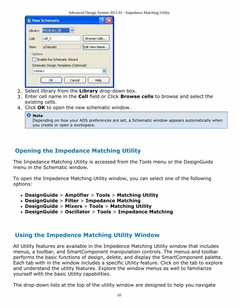
Select library from the Library drop-down box.2.Enter cell name in the Cell field or Click Browse cells to browse and select the3.existing cells.Click OK to open the new schematic window.4.
NoteDepending on how your ADS preferences are set, a Schematic window appears automatically whenyou create or open a workspace.
Opening the Impedance Matching Utility
The Impedance Matching Utility is accessed from the Tools menu or the DesignGuidemenu in the Schematic window.
To open the Impedence Matching Utility window, you can select one of the followingoptions:
DesignGuide > Amplifier > Tools > Matching UtilityDesignGuide > Filter > Impedance MatchingDesignGuide > Mixers > Tools > Matching UtilityDesignGuide > Oscillator > Tools > Impedance Matching
Using the Impedence Matching Utility Window
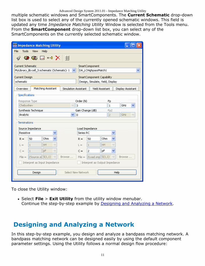
All Utility features are available in the Impedence Matching Utility window that includesmenus, a toolbar, and SmartComponent manipulation controls. The menus and toolbarperforms the basic functions of design, delete, and display the SmartComponent palette.Each tab with in the window includes a specific Utility feature. Click on the tab to exploreand understand the utility features. Explore the window menus as well to familiarizeyourself with the basic Utility capabilities.
The drop-down lists at the top of the utility window are designed to help you navigate
Advanced Design System 2011.01 - Impedance Matching Utility
11
multiple schematic windows and SmartComponents. The Current Schematic drop-downlist box is used to select any of the currently opened schematic windows. This field isupdated any time Impedance Matching Utility Window is selected from the Tools menu.From the SmartComponent drop-down list box, you can select any of theSmartComponents on the currently selected schematic window.
To close the Utility window:
Select File > Exit Utility from the utility window menubar.Continue the step-by-step example by Designing and Analyzing a Network.
Designing and Analyzing a NetworkIn this step-by-step example, you design and analyze a bandpass matching network. Abandpass matching network can be designed easily by using the default componentparameter settings. Using the Utility follows a normal design flow procedure:
Advanced Design System 2011.01 - Impedance Matching Utility
12
Select a component needed for your design from the component palette (Displayingthe SmartComponent Palette) and placing the component in your design (PlacingExample Component in the Design).
Provide specifications (Changing SmartComponent Parameters).
Design and analyze the component (Designing the Matching Component) andAnalyzing Yield of the Matching Network).
NoteBefore starting this section of the step-by-step example, confirm your setup (Setting Up the DesignEnvironment).
Displaying the SmartComponent Palette
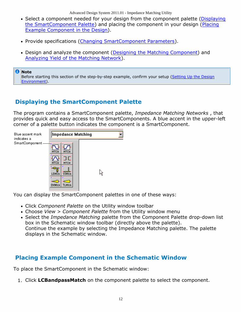
The program contains a SmartComponent palette, Impedance Matching Networks , thatprovides quick and easy access to the SmartComponents. A blue accent in the upper-leftcorner of a palette button indicates the component is a SmartComponent.
You can display the SmartComponent palettes in one of these ways:
Click Component Palette on the Utility window toolbarChoose View > Component Palette from the Utility window menuSelect the Impedance Matching palette from the Component Palette drop-down listbox in the Schematic window toolbar (directly above the palette).Continue the example by selecting the Impedance Matching palette. The palettedisplays in the Schematic window.
Placing Example Component in the Schematic Window
To place the SmartComponent in the Schematic window:
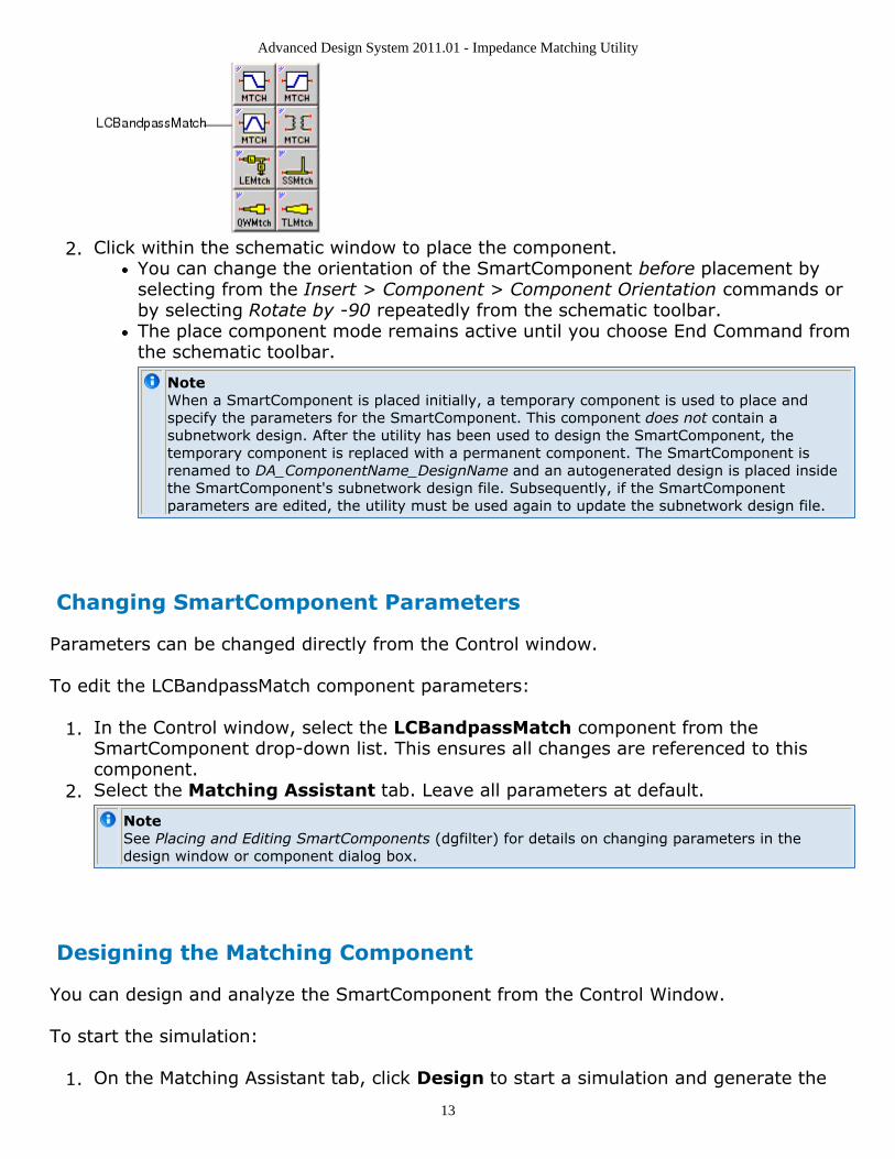
Click LCBandpassMatch on the component palette to select the component.1.
Advanced Design System 2011.01 - Impedance Matching Utility
13
Click within the schematic window to place the component.2.You can change the orientation of the SmartComponent before placement byselecting from the Insert > Component > Component Orientation commands orby selecting Rotate by -90 repeatedly from the schematic toolbar.The place component mode remains active until you choose End Command fromthe schematic toolbar.
NoteWhen a SmartComponent is placed initially, a temporary component is used to place andspecify the parameters for the SmartComponent. This component does not contain asubnetwork design. After the utility has been used to design the SmartComponent, thetemporary component is replaced with a permanent component. The SmartComponent isrenamed to DA_ComponentName_DesignName and an autogenerated design is placed insidethe SmartComponent's subnetwork design file. Subsequently, if the SmartComponentparameters are edited, the utility must be used again to update the subnetwork design file.
Changing SmartComponent Parameters
Parameters can be changed directly from the Control window.
To edit the LCBandpassMatch component parameters:
In the Control window, select the LCBandpassMatch component from the1.SmartComponent drop-down list. This ensures all changes are referenced to thiscomponent.Select the Matching Assistant tab. Leave all parameters at default.2.
NoteSee Placing and Editing SmartComponents (dgfilter) for details on changing parameters in thedesign window or component dialog box.
Designing the Matching Component
You can design and analyze the SmartComponent from the Control Window.
To start the simulation:
On the Matching Assistant tab, click Design to start a simulation and generate the1.
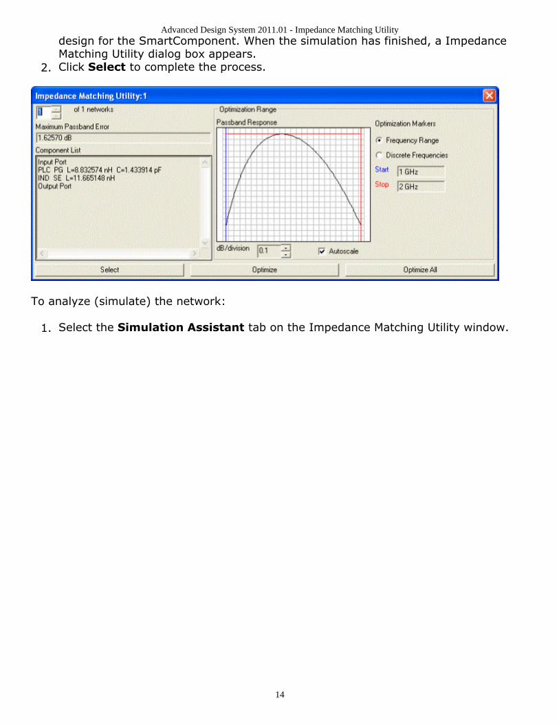
Advanced Design System 2011.01 - Impedance Matching Utility
14
design for the SmartComponent. When the simulation has finished, a ImpedanceMatching Utility dialog box appears.Click Select to complete the process.2.
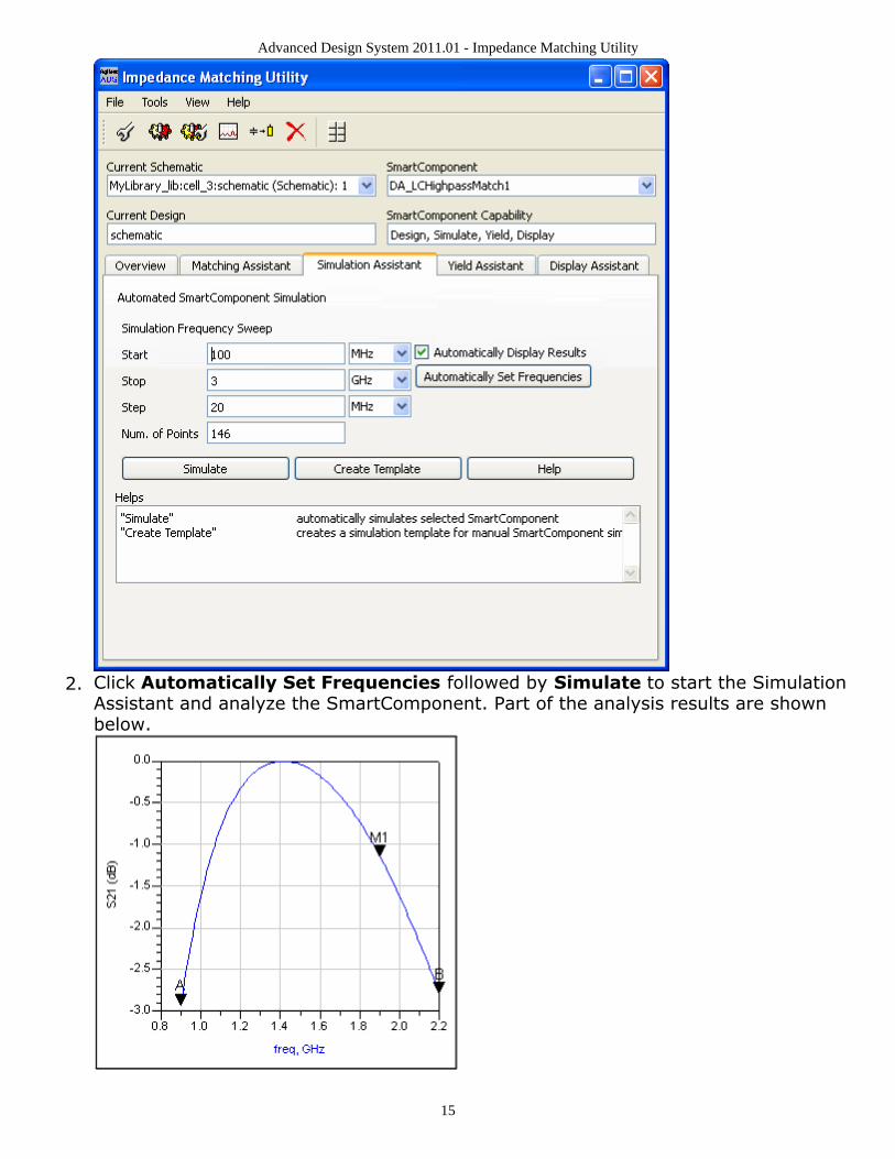
To analyze (simulate) the network:
Select the Simulation Assistant tab on the Impedance Matching Utility window.1.
Advanced Design System 2011.01 - Impedance Matching Utility
15
Click Automatically Set Frequencies followed by Simulate to start the Simulation2.Assistant and analyze the SmartComponent. Part of the analysis results are shownbelow.

Advanced Design System 2011.01 - Impedance Matching Utility
16
Closing the Matching Component Results Window
To close the display window, choose File > Close Window from the menu.
Examining the Matching Component Design
You can look at the details of the autogenerated design inside the SmartComponent'ssubnetwork.To examine the component's subnetwork:
Select the component LCBandpassMatch .1.Click Push Into Hierarchy on the schematic toolbar.2.After examining the design, click Pop Out on the schematic toolbar to close the view.3.
Analyzing Yield of the Matching Network
After the design process, the component sensitivities of the matching network can bechecked using the Yield Assistant .To find components to analyze:
Click the Yield Assistant tab on the Impedance Matching Utility window.1.

Advanced Design System 2011.01 - Impedance Matching Utility
17
Click View Components > Modify Statistics/Optimization . The matching2.network displays in the schematic along with a dialog box.
To choose components:
Choose Enabled from the Statistics Status drop-down menu.1.

Advanced Design System 2011.01 - Impedance Matching Utility
18
Select Next to move on to the next component. Repeat this until all 3 components in2.the network are enabled, and then click Done .Click Close in the Statistical Component Values dialog box.3.
To analyze yield sensitivity of the network:
In the Yield Assistant tab, select Automatically Set Frequencies .1.Select by Simulate to start the Yield Assistant and analyze the yield sensitivity to2.the selected component values. The results display automatically. The sensitivityhistogram for component C1 is shown here.
To close the display window, choose File > Close from the menu.3.
Advanced Design System 2011.01 - Impedance Matching Utility
19
Deleting the Matching SmartComponent
To delete the LCBandpassMatch SmartComponent, choose Tools > DeleteSmartComponent from the Control window.
NoteThe Delete button on the Control window is different from the Delete button on the ADS schematicwindow toolbar.
This completes the step-by-step example.
Advanced Design System 2011.01 - Impedance Matching Utility
20
SmartComponent Reference forImpedance Matching UtilityThis section contains detailed information for each Impedance Matching UtilitySmartComponents.
LCLowpassMatch (Lowpass Match) (impmatchutil)
LCHighpassMatch (Highpass Match) (impmatchutil)
LCBandpassMatch (Bandpass Match) (impmatchutil)
LCBandpassTransformer (Bandpass Transformer) (impmatchutil)
SingleStubMatch (Single-Stub Match) (impmatchutil)
QuarterWaveMatch (Quarter Wave Match) (impmatchutil)
TaperedLineMatch (Tapered Line Match) (impmatchutil)
LCEllMatch (Two-Element Ell Narrowband Match) (impmatchutil)
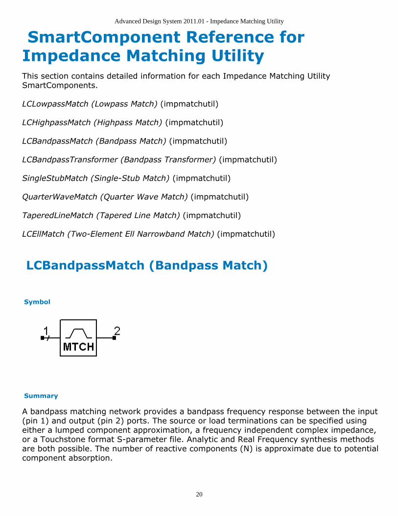
LCBandpassMatch (Bandpass Match)
Symbol
Summary
A bandpass matching network provides a bandpass frequency response between the input(pin 1) and output (pin 2) ports. The source or load terminations can be specified usingeither a lumped component approximation, a frequency independent complex impedance,or a Touchstone format S-parameter file. Analytic and Real Frequency synthesis methodsare both possible. The number of reactive components (N) is approximate due to potentialcomponent absorption.

Advanced Design System 2011.01 - Impedance Matching Utility
21
Parameters
Name Description Unit Default
Fp1 Frequency at lower passband edge GHz 1
Fp2 Frequency at upper passband edge GHz 2
SynthesisType Synthesis procedure, Analytic or Real Frequency (impmatchutil) None Analytic
GainChange Linear gain change over passband (can be negative) dB 0
N Network order None 3
SourceType Type of source impedance None Resistive
Rg Source resistance Ohms 50
Lg Source inductance nH 1
Cg Source capacitance pF 1
Zg Source impedance Ohms 50+j×50
SourceFile Source S-parameter file name None ZSource.s1p
SourceFileSparm Source S-parameter None "S(1,1)"
SourceImpType Complex source impedance interpretation None Source Impedance
LoadType Type of load impedance None Series RLC
RL Load resistance Ohms 50
LL Load inductance nH 1
CL Load capacitance pF 1
ZL Load impedance Ohms 100-j*100
LoadFile Load S-parameter file name None ZLoad.s1p
LoadFileSparm Load S-parameter None "S(1,1)"
LoadImpType Complex load impedance interpretation None Load Impedance
Palette
Filter DG - All Networks
Available Automated-Assistants
Matching Assistant, Simulation Assistant, Yield Assistant, Display Assistant
Matching Assistant Usage
For general information, refer to Matching Assistant (dgfilter).Network order results inapproximately 2×N elements, although this varies due to component absorption as well asrequired network transformations.
Simulation Assistant Usage
Advanced Design System 2011.01 - Impedance Matching Utility
22
For general information, refer to Simulation Assistant (dgfilter).
Yield Assistant Usage
For general information, refer to Yield Assistant (dgfilter).
Display Assistant Usage
For general information, refer to Display Assistant (dgfilter).
Example
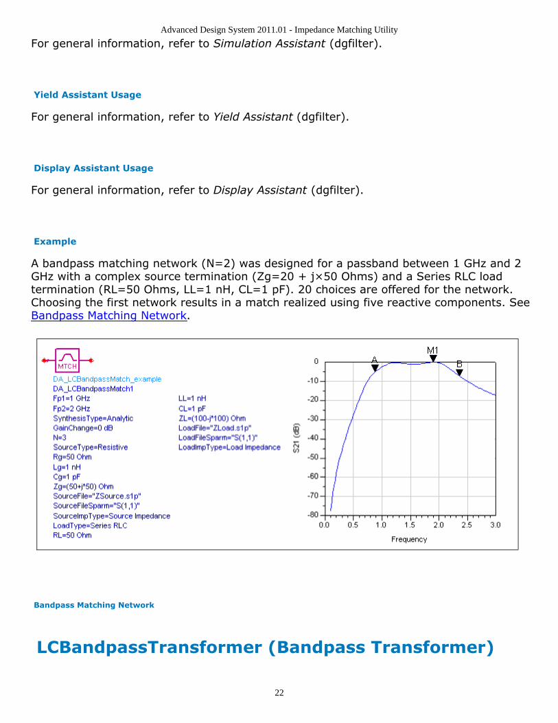
A bandpass matching network (N=2) was designed for a passband between 1 GHz and 2GHz with a complex source termination (Zg=20 + j×50 Ohms) and a Series RLC loadtermination (RL=50 Ohms, LL=1 nH, CL=1 pF). 20 choices are offered for the network.Choosing the first network results in a match realized using five reactive components. SeeBandpass Matching Network.
Bandpass Matching Network
LCBandpassTransformer (Bandpass Transformer)
Advanced Design System 2011.01 - Impedance Matching Utility
23
Symbol
Summary
A bandpass transformer provides a bandpass (pseudo-lowpass) frequency responsebetween the input (pin 1) and output (pin 2) ports. The source or load terminations mustbe real and unequal.
Parameters
Name Description Unit Default
Fp1 Frequency at left passband edge GHz 1
Fp2 Frequency at right passband edge GHz 2
N Network order None 3
ResponseType Type of frequency response None Maximally Flat
Rg Source resistance Ohms 50
RL Load resistance Ohms 25
Palette
Filter DG - All Networks
Available Automated-Assistants
Matching Assistant, Simulation Assistant, Yield Assistant, Display Assistant
Matching Assistant Usage
For general information, refer to Matching Assistant (dgfilter). The terminations must beunequal or no network is synthesized. For equal terminations, use a doubly-terminatedfilter topology. Network order results in 2×N components.
Simulation Assistant Usage
Advanced Design System 2011.01 - Impedance Matching Utility
24
Simulation Assistant Usage
For general information, refer to Simulation Assistant (dgfilter).
Yield Assistant Usage
For general information, refer to Yield Assistant (dgfilter).
Display Assistant Usage
For general information, refer to Display Assistant (dgfilter).
Example
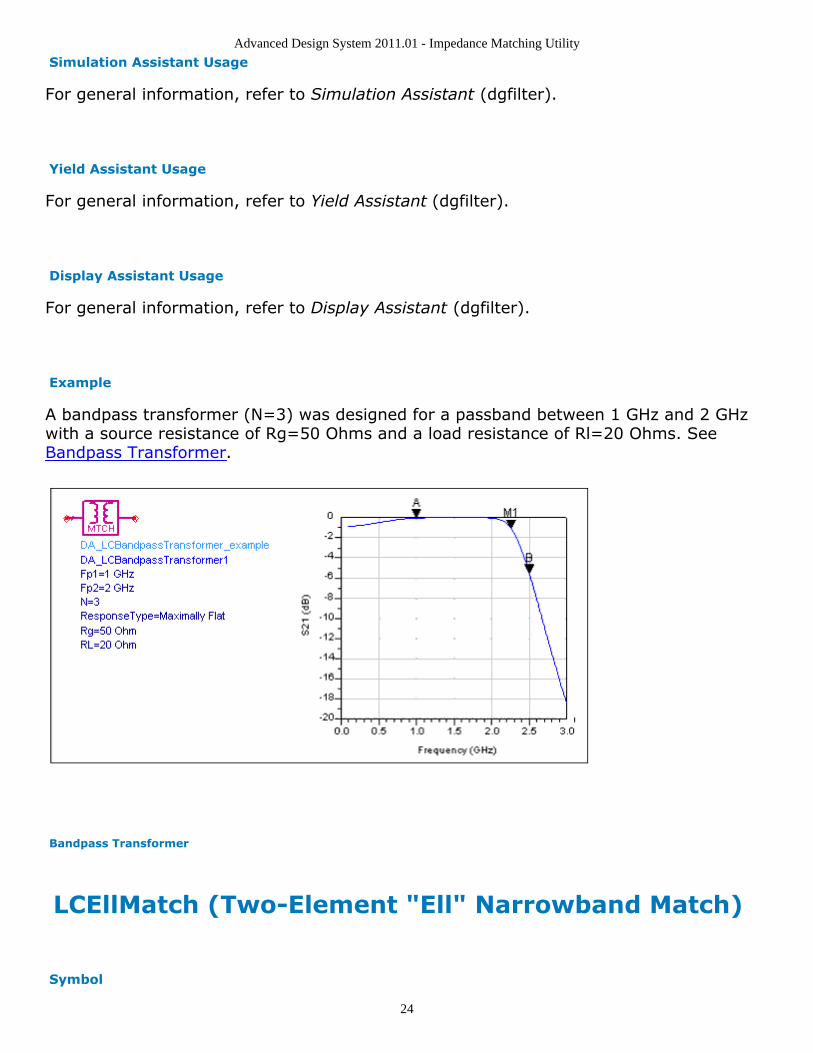
A bandpass transformer (N=3) was designed for a passband between 1 GHz and 2 GHzwith a source resistance of Rg=50 Ohms and a load resistance of Rl=20 Ohms. SeeBandpass Transformer.
Bandpass Transformer
LCEllMatch (Two-Element "Ell" Narrowband Match)
Symbol

Advanced Design System 2011.01 - Impedance Matching Utility
25
Summary
An Ell matching network provides a narrowband bandpass frequency response betweenthe input (pin 1) and output (pin 2) ports. The source or load terminations can bespecified using either a lumped component approximation, a frequency independentcomplex impedance, or a Touchstone format S-parameter file.
Parameters
Name Description Unit Default
F Frequency at center GHz 1
SourceType Type of source impedance None Resistive
Rg Source resistance Ohms 50
Lg Source inductance nH 1
Cg Source capacitance pF 1
Zg Source impedance Ohms 50+j×50
SourceFile Source S-parameter file name None ZSource.s1p
SourceFileSparm Source S-parameter None "S(1,1)"
SourceImpType Complex source impedance interpretation None Source Impedance
LoadType Type of load impedance None Series RL
RL Load resistance Ohms 100
LL Load inductance nH 1
CL Load capacitance pF 1
ZL Load impedance Ohms 100-j*100
LoadFile Load S-parameter file name None ZLoad.s1p
LoadFileSparm Load S-parameter None "S(1,1)"
LoadImpType Complex load impedance interpretation None Load Impedance
Palette
Impedance Matching
Available Automated-Assistants

Advanced Design System 2011.01 - Impedance Matching Utility
26
Matching Assistant, Simulation Assistant, Yield Assistant, Display Assistant,Transformation Assistant
Matching Assistant Usage
For general information, refer to Matching Assistant (dgfilter).
Simulation Assistant Usage
For general information, refer to Simulation Assistant (dgfilter).
Yield Assistant Usage
For general information, refer to Yield Assistant (dgfilter).
Display Assistant Usage
For general information, refer to Display Assistant (dgfilter).
Example
An Ell matching network was designed for a center frequency of 1 GHz with a 50 Ohmsource resistance and a Series RLC load termination (RL=50 Ohms, LL=1 nH, C =1 pF).

Advanced Design System 2011.01 - Impedance Matching Utility
27
Ell Matching Network
LCHighpassMatch (Highpass Match)
Symbol
Summary
A highpass matching network provides a highpass frequency response between the input(pin 1) and output (pin 2) ports. The source or load terminations can be specified usingeither a lumped component approximation, a frequency independent complex impedance,or a Touchstone format S-parameter file. Analytic and Real Frequency synthesis methodsare both possible. The network order (N) is approximate due to potential componentabsorption.
Parameters
Advanced Design System 2011.01 - Impedance Matching Utility
28
Name Description Unit Default
Fp Frequency at passband edge GHz 1
SynthesisType Synthesis procedure, Analytic or Real Frequency (impmatchutil) None Analytic
GainChange Linear gain change over passband (can be negative) dB 0
N Network order None 3
SourceType Type of source impedance None Resistive
Rg Source resistance Ohms 50
Lg Source inductance nH 1
Cg Source capacitance pF 1
Zg Source impedance Ohms 50+j×50
SourceFile Source S-parameter file name None ZSource.s1p
SourceFileSparm Source S-parameter None "S(1,1)"
SourceImpType Complex source impedance interpretation None Source Impedance
LoadType Type of load impedance None Series RC
RL Load resistance Ohms 50
LL Load inductance nH 1
CL Load capacitance pF 2
ZL Load impedance Ohms 100-j*100
LoadFile Load S-parameter file name None ZLoad.s1p
LoadFileSparm Load S-parameter None "S(1,1)"
LoadImpType Load impedance None Load Impedance
Palette
Filter DG - All Networks
Available Automated-Assistants
Matching Assistant, Simulation Assistant, Yield Assistant, Display Assistant
Matching Assistant Usage
For general information, refer to Matching Assistant (dgfilter). When representing thesource and/or load using lumped components, only lowpass type networks are allowed.Arbitrary terminations can be implemented using S-parameter files. However, if thespecified termination impedance is not of lowpass form, the resulting matching networkresponse approximates a lowpass form but typically rolls off at the low end of the band.
Simulation Assistant Usage
For general information, refer to Simulation Assistant (dgfilter).
Advanced Design System 2011.01 - Impedance Matching Utility
29
Yield Assistant Usage
For general information, refer to Yield Assistant (dgfilter).
Display Assistant Usage
For general information, refer to Display Assistant (dgfilter).
Example
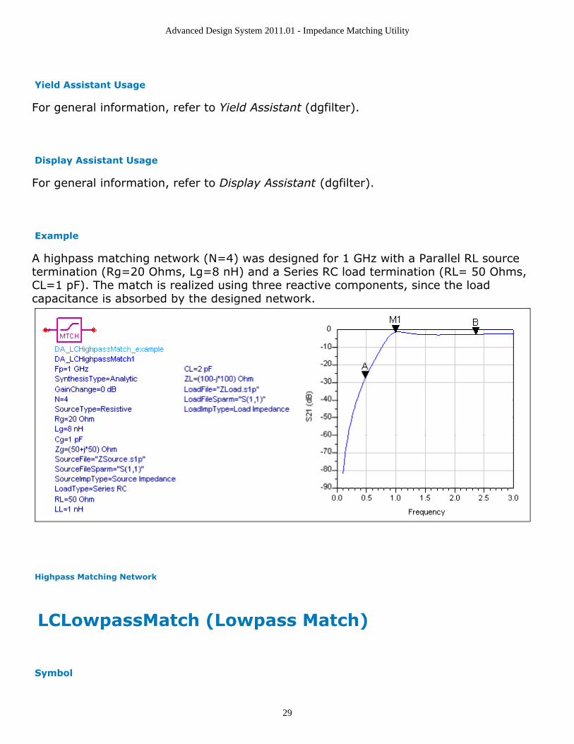
A highpass matching network (N=4) was designed for 1 GHz with a Parallel RL sourcetermination (Rg=20 Ohms, Lg=8 nH) and a Series RC load termination (RL= 50 Ohms,CL=1 pF). The match is realized using three reactive components, since the loadcapacitance is absorbed by the designed network.
Highpass Matching Network
LCLowpassMatch (Lowpass Match)
Symbol
Advanced Design System 2011.01 - Impedance Matching Utility
30
Summary
A lowpass matching network provides a lowpass frequency response between the input(pin 1) and output (pin 2) ports. The source or load terminations can be specified usingeither a lumped component approximation, a frequency independent complex impedance,or a Touchstone format S-parameter file. Analytic and Real Frequency synthesis methodsare both possible. The network order (N) is approximate due to potential componentabsorption.
Parameters
Name Description Unit Default
Fp Frequency at passband edge GHz 1
SynthesisType Synthesis procedure, Analytic or Real Frequency (impmatchutil) None Analytic
GainChange Linear gain change over passband (can be negative) dB 0
N Network order None 3
SourceType Type of source impedance None Resistive
Rg Source resistance Ohms 50
Lg Source inductance nH 1
Cg Source capacitance pF 1
Zg Source impedance Ohms 50+j×50
SourceFile Source S-parameter file name None ZSource.s1p
SourceFileSparm Source S-parameter None "S(1,1)"
SourceImpType Complex source impedance interpretation None Source Impedance
LoadType Type of load impedance None Series RL
RL Load resistance Ohms 50
LL Load inductance nH 1
CL Load capacitance pF 1
ZL Load impedance Ohms 100-j*100
LoadFile Load S-parameter file name None ZLoad.s1p
LoadFileSparm Load S-parameter None "S(1,1)"
LoadImpType Complex load impedance interpretation None Load Impedance
Palette
Filter DG - All Networks

Advanced Design System 2011.01 - Impedance Matching Utility
31
Available Automated-Assistants
Matching Assistant, Simulation Assistant, Yield Assistant, Display Assistant
Matching Assistant Usage
For general information, refer to Matching Assistant (dgfilter). When representing thesource and/or load using lumped components only lowpass type networks are allowed.Arbitrary terminations can be implemented using S-parameter files. However, if thespecified termination impedance is not of lowpass form, the resulting matching networkresponse approximates a lowpass form but typically rolls off at the low end of the band.
Simulation Assistant Usage
For general information, refer to Simulation Assistant (dgfilter).
Yield Assistant Usage
For general information, refer to Yield Assistant (dgfilter).
Display Assistant Usage
For general information, refer to Display Assistant (dgfilter).
Example
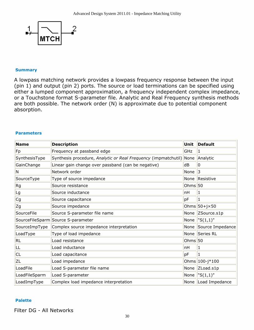
A lowpass matching network (N=3) was designed for 1 GHz with a resistive sourcetermination (Rg=50 Ohms) and a Series RL load termination (RL=50 Ohms, LL=1 nH).The match is realized using two reactive components, since the load inductance isabsorbed by the designed network.
Advanced Design System 2011.01 - Impedance Matching Utility
32
Lowpass Matching Network
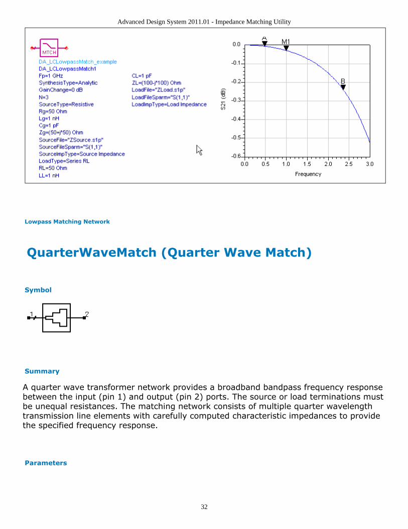
QuarterWaveMatch (Quarter Wave Match)
Symbol
Summary
A quarter wave transformer network provides a broadband bandpass frequency responsebetween the input (pin 1) and output (pin 2) ports. The source or load terminations mustbe unequal resistances. The matching network consists of multiple quarter wavelengthtransmission line elements with carefully computed characteristic impedances to providethe specified frequency response.
Parameters
Advanced Design System 2011.01 - Impedance Matching Utility
33
Name Description Unit Default
Fp1 Frequency at lower passband edge GHz 1
Fp2 Frequency at upper passband edge GHz 2
Rg Input impedance Ohms 50
RL Load impedance Ohms 100
ResponseType Type of frequency response None Uniform
N Number of Quarter-Wave Sections (set N=0 to compute N) None 0
Rmax Maximum voltage reflection coefficient dB 20
Palette
Impedance Matching
Available Automated-Assistants
Matching Assistant, Simulation Assistant, Yield Assistant, Display Assistant,Transformation Assistant
Matching Assistant Usage
For general information, refer to Matching Assistant (dgfilter).
Simulation Assistant Usage
For general information, refer to Simulation Assistant (dgfilter).
Yield Assistant Usage
For general information, refer to Yield Assistant (dgfilter).
Display Assistant Usage
For general information, refer to Display Assistant (dgfilter).
Example
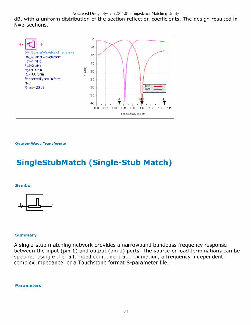
A quarter wave transformer was designed to match a 100 Ohm load impedance to a 50ohm source impedance from 1GHz to 2 GHz. The maximum reflection coefficient was -20
Advanced Design System 2011.01 - Impedance Matching Utility
34
dB, with a uniform distribution of the section reflection coefficients. The design resulted inN=3 sections.
Quarter Wave Transformer
SingleStubMatch (Single-Stub Match)
Symbol
Summary
A single-stub matching network provides a narrowband bandpass frequency responsebetween the input (pin 1) and output (pin 2) ports. The source or load terminations can bespecified using either a lumped component approximation, a frequency independentcomplex impedance, or a Touchstone format S-parameter file.
Parameters

Advanced Design System 2011.01 - Impedance Matching Utility
35
Name Description Unit Default
F Frequency at center GHz 1
Zstub Characteristic Impedance of stub line Ohm 50
Zline Characteristic Impedance of line between load and stub Ohm 50
SourceType Type of source impedance None Resistive
Rg Source resistance Ohms 50
Lg Source inductance nH 1
Cg Source capacitance pF 1
Zg Source impedance Ohms 50+j×50
SourceFile Source S-parameter file name None ZSource.s1p
SourceFileSparm Source S-parameter None "S(1,1)"
SourceImpType Complex source impedance interpretation None Source Impedance
LoadType Type of load impedance None Series RL
RL Load resistance Ohms 100
LL Load inductance nH 1
CL Load capacitance pF 1
ZL Load impedance Ohms 100-j*100
LoadFile Load S-parameter file name None ZLoad.s1p
LoadFileSparm Load S-parameter None "S(1,1)"
LoadImpType Complex load impedance interpretation None Load Impedance
Palette
Impedance Matching
Available Automated-Assistants
Matching Assistant, Simulation Assistant, Yield Assistant, Display Assistant,Transformation Assistant
Matching Assistant Usage
For general information, refer to Matching Assistant (dgfilter).
Simulation Assistant Usage
For general information, refer to Simulation Assistant (dgfilter).
Yield Assistant Usage

Advanced Design System 2011.01 - Impedance Matching Utility
36
For general information, refer to Yield Assistant (dgfilter).
Display Assistant Usage
For general information, refer to Display Assistant (dgfilter).
Example
A single-stub matching network was designed to match a Series RL (R=100 Ohms, L =1nH) load impedance to a 50 ohm source impedance at a center frequency of 1 GHz.Choosing the configuration with an open-circuit stub yielded a design offering the resultsshown in the illustration below, Single-stub Matching Network.
Single-stub Matching Network
TaperedLineMatch (Tapered Line Match)
Symbol

Advanced Design System 2011.01 - Impedance Matching Utility
37
Summary
A tapered line transformer network provides a broadband highpass frequency responsebetween the input (pin 1) and output (pin 2) ports. The source or load terminations mustbe unequal resistances. The network consists of multiple transmission line sections toapproximate a tapered line.
Parameters
Name Description Unit Default
Fp Frequency at lower passband edge (Response is Highpass) GHz 1
Rg Input impedance Ohms 50
RL Load impedance Ohms 100
ResponseType Type of frequency response None Exponential Taper
Rmax Maximum voltage reflection coefficient dB -20
N Number of TLine Sections per wavelength None 0
Palette
Impedance Matching
Available Automated-Assistants
Matching Assistant, Simulation Assistant, Yield Assistant, Display Assistant,Transformation Assistant
Matching Assistant Usage
For general information, refer to Matching Assistant (dgfilter).
Simulation Assistant Usage
For general information, refer to Simulation Assistant (dgfilter).
Yield Assistant Usage
For general information, refer to Yield Assistant (dgfilter).
Advanced Design System 2011.01 - Impedance Matching Utility
38
Display Assistant Usage
For general information, refer to Display Assistant (dgfilter).
Example
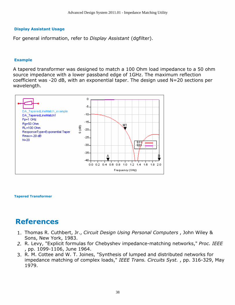
A tapered transformer was designed to match a 100 Ohm load impedance to a 50 ohmsource impedance with a lower passband edge of 1GHz. The maximum reflectioncoefficient was -20 dB, with an exponential taper. The design used N=20 sections perwavelength.
Tapered Transformer
ReferencesThomas R. Cuthbert, Jr., Circuit Design Using Personal Computers , John Wiley &1.Sons, New York, 1983.R. Levy, "Explicit formulas for Chebyshev impedance-matching networks," Proc. IEEE2., pp. 1099-1106, June 1964.R. M. Cottee and W. T. Joines, "Synthesis of lumped and distributed networks for3.impedance matching of complex loads," IEEE Trans. Circuits Syst. , pp. 316-329, May1979.

Advanced Design System 2011.01 - Impedance Matching Utility
39
Using Automated Assistants inImpedance Matching UtilityThis section describes the Automated Assistants available in this Utility.
Automated Design and AnalysisThe Automated Assistants provide quick design, simulation, yield analysis, andperformance display for SmartComponents and enable transformation of lumped elementsto transmission line elements. Five Automated Assistants are available in this Utility:
Matching Assistant (dgfilter) is used to generate and update the design containedwithin a matching or transformer SmartComponent from the given specifications.
Simulation Assistant (dgfilter) is used to analyze the design contained within aSmartComponent.
Yield Assistant (dgfilter) is used to analyze the design sensitivities contained within aSmartComponent.
Display Assistant (dgfilter) is used to easily and quickly display the performance of aSmartComponent.
Transformation Assistant (dgfilter) is used to transform an ideal filter topology to aform that is realizable for high-frequency systems.
Explore each tab page by selecting the associated tab on the control window.
Matching Assistant The Matching Assistant is used to generate and update the design contained within amatching or transformer SmartComponent from the given specifications. This tool isaccessed using the Matching Utility window. From the utility window, full design control is

Advanced Design System 2011.01 - Impedance Matching Utility
40
enabled from the Matching Assistant tab. Component design operations can also beaccomplished using the utility window menu and toolbar. Any parameter change madefrom the Matching Assistant tab is reflected on the SmartComponent in the schematic.
To view a SmartComponent, select the SmartComponent from the SmartComponent drop-down list box in the upper right corner of the utility window. The SmartComponentparameters are shown inside the Matching Assistant tab.
Matching Assistant SmartComponents
The Matching Assistant SmartComponents include lumped and distributed elementmatching networks and transformers.
Matching Networks
Matching networks provide a match between two real or complex impedances over a givenfrequency range. The response can be lowpass, highpass, or bandpass if allowed by thespecified impedance termination.
Transformers
Transformers provide a bandpass match between two unequal but real impedances usinga special transform of a lowpass filter network.
Specifications

Advanced Design System 2011.01 - Impedance Matching Utility
41
ResponseType - frequency response type for transformer networks. Choices consistof Maximally Flat , Chebyshev , Bessel-Thompson , and Gaussian . This menu is usedfor transformers only.Synthesis Technique - Method used to synthesize the matching network - Analytic orReal Frequency . This menu is used for matching networks only.Order - The network order. This is approximately the number of reactive componentsfor lowpass and highpass matching networks. For bandpass matching networks ortransformers, the number of reactive components is approximately twice the order(exactly twice for transformers). For matching networks, absorption of source andload reactances as well as component transformations can change this number.Gain Change - Gain Change in dB over the band for matching networks. Duringsynthesis, this parameter is ignored. However, if optimization is selected, this slopewill be applied as part of the optimization goal. This parameter must be positive. Thetarget gain will start at the left passband edge at -(Gain Change) and ramp linearly(in dB) to 0. This field is used for matching networks only.Fp1, Fp2 - Lower and upper passband edge frequencies in Hertz. For lowpass andhighpass networks, Fp2 is not used and Fp1 is changed to Fp to represent thepassband edge frequency. Frequency values are changed by entering new values inthe edit box. Units are changed by selecting a new unit identifier from the drop-downmenu.Line Impedance, Stub Impedance - Characteristic impedance of transmission linesand stubs used in distributed element matching networks.Max Reflection Coeff - Maximum reflection coefficient in the passband for certaindistributed element matching networks.# Sections/Wavelength - Number of transmission line segments per wavelength touse to approximate linear taper with transmission line elements.
Terminations
For transformers, the terminations must be resistive with unequal values. As such, onlythe R input boxes are available for transformers. For other matching networks, theterminations can be input using lumped components networks, complex impedances, andS-parameter files. Usage for these different types is:
Lumped Component - Choices include Resistive, Series RL, Series RC, Parallel RL,Parallel RC, Series RLC, Parallel RLC, where R = resistance, L = inductance, and C =capacitance. Component values must be specified by the user. For lowpass networks,choices are limited to Resistive, Series RL, and Parallel RC. For highpass networks,choices are limited to Resistive, Series RC, and Parallel RL.Complex Impedance - The impedance is interpreted as frequency independent,expressed in the form 50 + j×10 Ohms. This input approach is useful for narrowbandmatching. If the true impedance varies significantly with frequency, better accuracyis obtained by specifying the termination using an S-parameter file or manuallyentering the data using the spreadsheet data entry capability.S-Parameter File - Any termination can be represented using a file in Touchstoneformat representing 1-port parameters ( *.s1p ). The impedance can be specified in

Advanced Design System 2011.01 - Impedance Matching Utility
42
S, Z, or Y parameters. For details on data file format, refer to the Circuit Simulationmanual under SnP format . The Browse button launches a window to enable selectionof the file.Manual Data Entry - The complex impedance - specified as an impedance,admittance, or reflection coefficient - can be entered as a function of frequencymanually. When the source or load impedance is specified as Manual Entry, the Editbutton can be used to open a spreadsheet useful for entering frequency/impedancepairs.
Interpret as Input/Output Impedance - These options are available for three cases ofsource and load impedance; complex load, S-parameter file, and Manual entry. Usethe Interpret as Input Impedance option to specify that the value you have entered isof impedance looking into the device (S-parameters of the measured device, forinstance). Use the Interpret as Output Impedance option to specify that the valueyou have entered is of impedance looking out from the device (impedance you wantto see). For more information, see Designing with an S2P File (dgfilter).
Design
The design is accomplished using one of the these methods.
Click Design on the Matching Assistant tab.Click Design on the utility window toolbar.Choose Tools > Auto-Design from the utility window menu.After completion of the synthesis, a dialog box appears.

Advanced Design System 2011.01 - Impedance Matching Utility
43
Optimization range
All networks can be viewed using the spin box. Each network can be viewed in two places:
Dialog Box - Shows a text based description of the current network.Schematic Window - Shows the actual drawing of the current network.
For each network, the maximum error in the passband response in dB (taken with respectto the ideal flat or sloped response) appears in the dialog box. The response over thespecified passband is also shown in an interactive graph. The scale on this graph can bechanged manually using the spin box immediately below the graph. Checking theAutoscale box will automatically choose the scale to fit the response within the graph area.
The response of the matching network can be optimized from this dialog by clicking theOptimize button. The vertical lines on the graph, which by default lie at the edges of theband, are markers used for specification of the optimization frequencies. These markerscan be moved by clicking and dragging them with the mouse, with the marker frequencybeing displayed in the corresponding text box to the right of the plot (the markers andlabels for the text boxes are color coordinated). If the radio box for Frequency Range isselected, the optimization will be performed to minimize the Maximum Error over therange of frequencies between the two markers. If the radio box for Discrete Frequencies isselected, initially only a single marker is present. Up to three additional markers can beadded by clicking the appropriate Activate button. Each added marker can also beremoved by clicking the corresponding Deactivate button. Under this option, theoptimization will be performed to minimize the Maximum Error at the frequenciesindicated by the markers. Clicking the Optimize All button sequentially optimizes allnetworks found using the optimization parameters displayed. This optimization processcan be canceled from the progress indicator that appears after the optimizer is launched.After the optimization is complete, the updated network appears in the dialog box and onthe schematic.

Advanced Design System 2011.01 - Impedance Matching Utility
44
Discrete optimization points
Synthesis Technique
Two different techniques are available for lumped element matching network synthesis:Analytic and Real Frequency.
Analytic - For this method, a Chebyshev filter is chosen that can completely orpartially absorb the source and load reactances, as outlined in [1], [2]. If thespecified network order generates reactance topologies at the ends of the networkthat cannot absorb the specified terminations, the Utility informs the user that thenetwork order is increased by one. This synthesis procedure is very robust,particularly for terminations that are modeled as lumped components. Forterminations specified as a complex impedance, the Utility computes the simplestlumped component topology that produces this impedance at the band edge orcenter frequency. For terminations specified using an S-parameter file or manualentry, the Utility generates a lumped component model for the specified impedancevariation with frequency.Real Frequency - This method uses the basic Chebyshev matching capability of theAnalytic approach. However, application of the technique is modified by breaking thefrequency band into small pieces, performing the match over this small band byfinding a lumped component fit to the impedance given, and retaining the networkswith the lowest insertion loss. Typically, optimization is required to obtain a goodmatch over the entire passband. This approach is useful for loads that are not wellmodeled using the simple lumped component network choices given. For lowpass orhighpass networks with N = 2 or bandpass networks with N = 1, this methodsynthesizes narrowband 2 component matching networks (L networks), retainingthose that provide the best match over the band.Transformers - Lumped element transformers provide a pseudo-bandpass responseto match two real and unequal resistances over a specified frequency band. Theapproach uses a transformation of a lowpass filter network to achieve the match [1],

Advanced Design System 2011.01 - Impedance Matching Utility
45
[3]. The quality of the match in terms of passband error depends upon the frequencybandwidth chosen as well as the ratio of the terminating impedances. Distributedelement transformers create a true bandpass response over the band.Narrow Band Matching Networks - The lumped two element (Ell) matching networkas well as the single stub matching network provide exact matching at a singlefrequency.
Designing with an S2P File
Use these steps for designing with an S2P file:
For input match, start with a resistive source of 50 Ohms, load pointing to S11 of the1.S2P file. Design optimize "input match." You need to optimize repeatedly to improvethe performance, until you see not much change.For output match, start with S22 of the S2P file as source, load set to 50 Ohms.2.Design and optimize.
NoteYou do not have to set the interpret as input/output, so DO NOT choose those buttons at all whiledesigning with S2P files. This button essentially toggles whether the program takes the conjugate ofthe data you enter or not. Sometimes you collect impedance data for the device you have, orsometimes it is for the impedance you want. So, effectively, it changes the perspective of whetheryou are looking into the DUT or looking into the matching circuit. This is used mostly while using theManual entry mode for Impedances.
You can try using analytical or higher order to see whether you can improve the3.performance further.
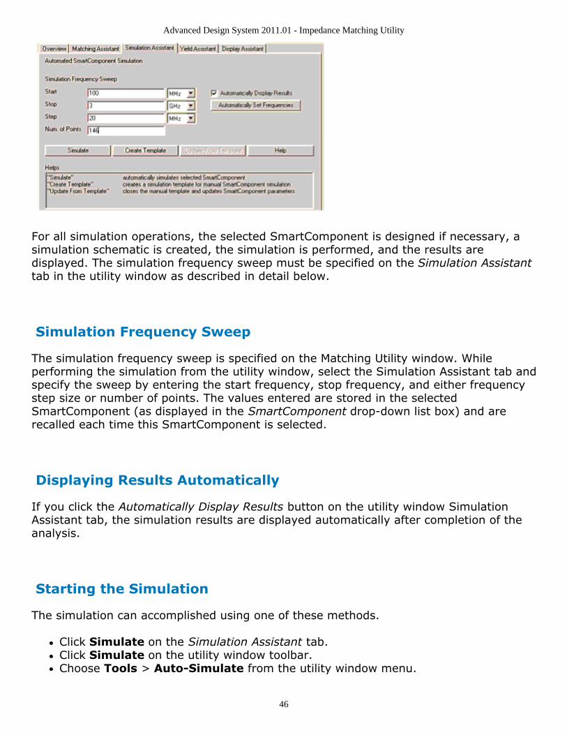
Simulation Assistant The Simulation Assistant is used to analyze the design contained within aSmartComponent. The Assistant creates a simulation circuit around the SmartComponent,then automatically performs the appropriate simulation. If set, the Assistant automaticallydisplays the simulation results.
The Simulation Assistant is accessed using the Matching Utility window, where fullsimulation control is enabled from the Simulation Assistant tab. Basic simulation can alsobe accomplished using the utility window menu and toolbar.
Advanced Design System 2011.01 - Impedance Matching Utility
46
For all simulation operations, the selected SmartComponent is designed if necessary, asimulation schematic is created, the simulation is performed, and the results aredisplayed. The simulation frequency sweep must be specified on the Simulation Assistanttab in the utility window as described in detail below.
Simulation Frequency Sweep
The simulation frequency sweep is specified on the Matching Utility window. Whileperforming the simulation from the utility window, select the Simulation Assistant tab andspecify the sweep by entering the start frequency, stop frequency, and either frequencystep size or number of points. The values entered are stored in the selectedSmartComponent (as displayed in the SmartComponent drop-down list box) and arerecalled each time this SmartComponent is selected.
Displaying Results Automatically
If you click the Automatically Display Results button on the utility window SimulationAssistant tab, the simulation results are displayed automatically after completion of theanalysis.
Starting the Simulation
The simulation can accomplished using one of these methods.
Click Simulate on the Simulation Assistant tab.Click Simulate on the utility window toolbar.Choose Tools > Auto-Simulate from the utility window menu.
Advanced Design System 2011.01 - Impedance Matching Utility
47
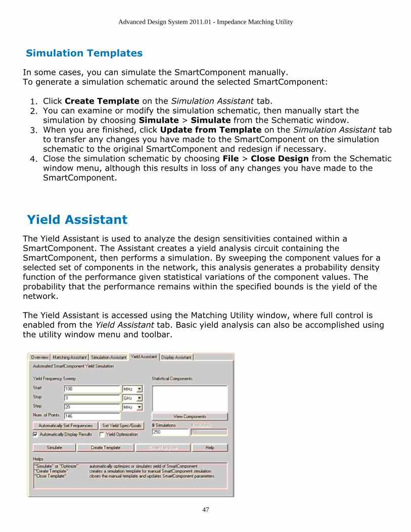
Simulation Templates
In some cases, you can simulate the SmartComponent manually.To generate a simulation schematic around the selected SmartComponent:
Click Create Template on the Simulation Assistant tab.1.You can examine or modify the simulation schematic, then manually start the2.simulation by choosing Simulate > Simulate from the Schematic window.When you are finished, click Update from Template on the Simulation Assistant tab3.to transfer any changes you have made to the SmartComponent on the simulationschematic to the original SmartComponent and redesign if necessary.Close the simulation schematic by choosing File > Close Design from the Schematic4.window menu, although this results in loss of any changes you have made to theSmartComponent.
Yield Assistant The Yield Assistant is used to analyze the design sensitivities contained within aSmartComponent. The Assistant creates a yield analysis circuit containing theSmartComponent, then performs a simulation. By sweeping the component values for aselected set of components in the network, this analysis generates a probability densityfunction of the performance given statistical variations of the component values. Theprobability that the performance remains within the specified bounds is the yield of thenetwork.
The Yield Assistant is accessed using the Matching Utility window, where full control isenabled from the Yield Assistant tab. Basic yield analysis can also be accomplished usingthe utility window menu and toolbar.

Advanced Design System 2011.01 - Impedance Matching Utility
48
The selected SmartComponent must be designed before yield analysis can be performed.The analysis proceeds by statistically sweeping the value of each selected component andanalyzing the impact of this component value variation on the frequency response of thenetwork.
Simulation Frequency Sweep
The simulation frequency sweep is specified on the Yield Assistant tab of the MatchingUtility window. From this tab, specify the sweep by entering the start frequency, stopfrequency, and either frequency step size or number of points. The values entered arestored in the selected SmartComponent (as displayed in the SmartComponent drop-downlist box) and are recalled each time this SmartComponent is selected.
Statistical Components
The Statistical Components list-box displays all components that are statistically variedduring simulation. Clicking Update opens the dialog box (shown below) to simplify theprocess of selecting components.
The matching network is shown in the schematic with the currently selected componenthighlighted. If you want this component value to be swept statistically during the analysis,select Enabled in the Statistics Status box. You can then specify the parameters of thestatistical sweep. After you have specified all parameters for a component, clicking Nexttakes you to the next component in the network. The analysis allows for a maximum of 4components to be selected at one time. After you have finished specification, you can clickDone from the dialog box to return to the Yield Assistant tab. Clicking View under theStatistical Components box opens a dialog box from which you can view a summary of the
Advanced Design System 2011.01 - Impedance Matching Utility
49
statistical parameters for each selected component. There are also buttons to take youdirectly to the Modify Component Parameters dialog from this summary dialog to facilitateediting of the statistical sweep parameters.
The # Simulations parameter specifies the number of Monte Carlo simulations that areused to estimate the statistical behavior of the network. Increasing the number ofsimulations increases the statistical sample size and therefore provide a better estimate ofthe performance at the expense of increased computational time.
Yield Optimization
The network component values can also be optimized so that the performance is lesssensitive to component value variations. This can be accomplished by selecting the YieldOptimization check box. In this case, the optimization requires that a set of performancegoals be specified for the network. The yield is defined as the probability that the networkfrequency response satisfies these performance specifications given the statisticalproperties of the individual components. Each component has a default set of goalsdepending on the type of response (lowpass, bandpass, etc.). Each goal specifies theinsertion loss performance of the network in dB and can represent a specification that thevalue stay above or below the stated level. The specification can be at a single point, orover a given frequency band. For a single frequency point, set the pulldown to "at", andset the frequency parameter. For a range of frequencies, set the pulldown to "from",which will activate both frequency parameters in order to specify the frequency range.To modify the default goals:
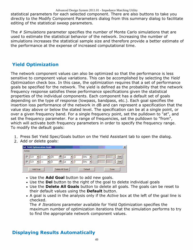
Press Set Yield Spec/Goals button on the Yield Assistant tab to open the dialog.1.Add or delete goals:2.
Use the Add Goal button to add new goals.Use the Del button to the right of the goal to delete individual goalsUse the Delete All Goals button to delete all goals. The goals can be reset totheir default values using the Default button.A goal is used in the analysis only if the Active box at the left of the goal line ischecked.The # Iterations parameter available for Yield Optimization specifies themaximum number of optimization iterations that the simulation performs to tryto find the appropriate network component values.
Displaying Results Automatically

Advanced Design System 2011.01 - Impedance Matching Utility
50
If the Automatically Display Results box on the utility window Yield Assistant tab isselected, the simulation results is displayed automatically after completion of the analysis.
Starting the Simulation
The yield analysis can accomplished using one of these methods.
Click the Simulate button on the Yield Assistant tab.Click the Simulate Yield button on the utility window toolbar.Choose Tools > Auto-Simulate Yield from the utility window menu.
Yield Results
For each component (up to a maximum of 4) chosen for yield analysis, a yield sensitivityhistogram is displayed. The yield definition can be changed on the first page of the displayby setting passband frequencies Fp_1 and Fp_2 as well as the maximum insertion loss atthese frequencies, and stopband frequencies Fs_1 and Fs_2 as well as the minimuminsertion loss at these frequencies. Other pages in the display show the overall statistics ofthe yield as well as the frequency response for each of the Monte Carlo simulations.
Yield Templates
In some cases, you can simulate the SmartComponent manually.To generate a simulation schematic around the selected SmartComponent:
Click Create Template on the Yield Assistant tab.1.After examining or modifying the simulation schematic, manually start the simulation2.by choosing Simulate > Simulate from the Schematic window.When you are finished, click the Close Template button on the Yield Assistant tab to3.return to the original design. You can also manually close the simulation schematicby choosing File > Close Design from the Schematic window menu.
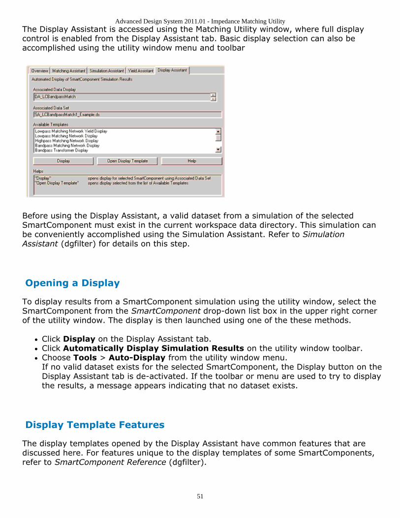
Display Assistant The Display Assistant is used to easily and quickly display the performance of aSmartComponent. The display templates are preconfigured display files that provide acomprehensive look at the performance of the component. You can create your owndisplays or modify the included display templates using the built in features of AdvancedDesign System, but in most situations, the included display templates provides all theinformation you need.
Advanced Design System 2011.01 - Impedance Matching Utility
51
The Display Assistant is accessed using the Matching Utility window, where full displaycontrol is enabled from the Display Assistant tab. Basic display selection can also beaccomplished using the utility window menu and toolbar
Before using the Display Assistant, a valid dataset from a simulation of the selectedSmartComponent must exist in the current workspace data directory. This simulation canbe conveniently accomplished using the Simulation Assistant. Refer to SimulationAssistant (dgfilter) for details on this step.
Opening a Display
To display results from a SmartComponent simulation using the utility window, select theSmartComponent from the SmartComponent drop-down list box in the upper right cornerof the utility window. The display is then launched using one of the these methods.
Click Display on the Display Assistant tab.Click Automatically Display Simulation Results on the utility window toolbar.Choose Tools > Auto-Display from the utility window menu.If no valid dataset exists for the selected SmartComponent, the Display button on theDisplay Assistant tab is de-activated. If the toolbar or menu are used to try to displaythe results, a message appears indicating that no dataset exists.
Display Template Features
The display templates opened by the Display Assistant have common features that arediscussed here. For features unique to the display templates of some SmartComponents,refer to SmartComponent Reference (dgfilter).

Advanced Design System 2011.01 - Impedance Matching Utility
52
Basic Layout
Basic Layout of Display Templates (dgfilter) shows the basic layout of the displaytemplates. Area one of the display template contains a graph of the most importantparameters of the SmartComponent. Area two contains several graphs that give acomprehensive look at the component's performance. Area three contains a table listingthe basic specifications and performance of the component.
Basic Layout of Display Templates
Typical Area One Graph
The following figure shows a typical graph from area one of a display template.
Basic Layout
Basic Layout of Display Templates (dgfilter) shows the basic layout of the displaytemplates. Area one of the display template contains a graph of the most important
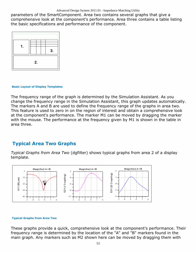
Advanced Design System 2011.01 - Impedance Matching Utility
53
parameters of the SmartComponent. Area two contains several graphs that give acomprehensive look at the component's performance. Area three contains a table listingthe basic specifications and performance of the component.
Basic Layout of Display Templates
The frequency range of the graph is determined by the Simulation Assistant. As youchange the frequency range in the Simulation Assistant, this graph updates automatically.The markers A and B are used to define the frequency range of the graphs in area two.This feature is used to zero in on the region of interest and obtain a comprehensive lookat the component's performance. The marker M1 can be moved by dragging the markerwith the mouse. The performance at the frequency given by M1 is shown in the table inarea three.
Typical Area Two Graphs
Typical Graphs from Area Two (dgfilter) shows typical graphs from area 2 of a displaytemplate.
Typical Graphs from Area Two
These graphs provide a quick, comprehensive look at the component's performance. Theirfrequency range is determined by the location of the "A" and "B" markers found in themain graph. Any markers such as M2 shown here can be moved by dragging them with
Advanced Design System 2011.01 - Impedance Matching Utility
54
the mouse. Performance criteria at the marker frequency displays in the table in areathree.
Typical Area Three Templates
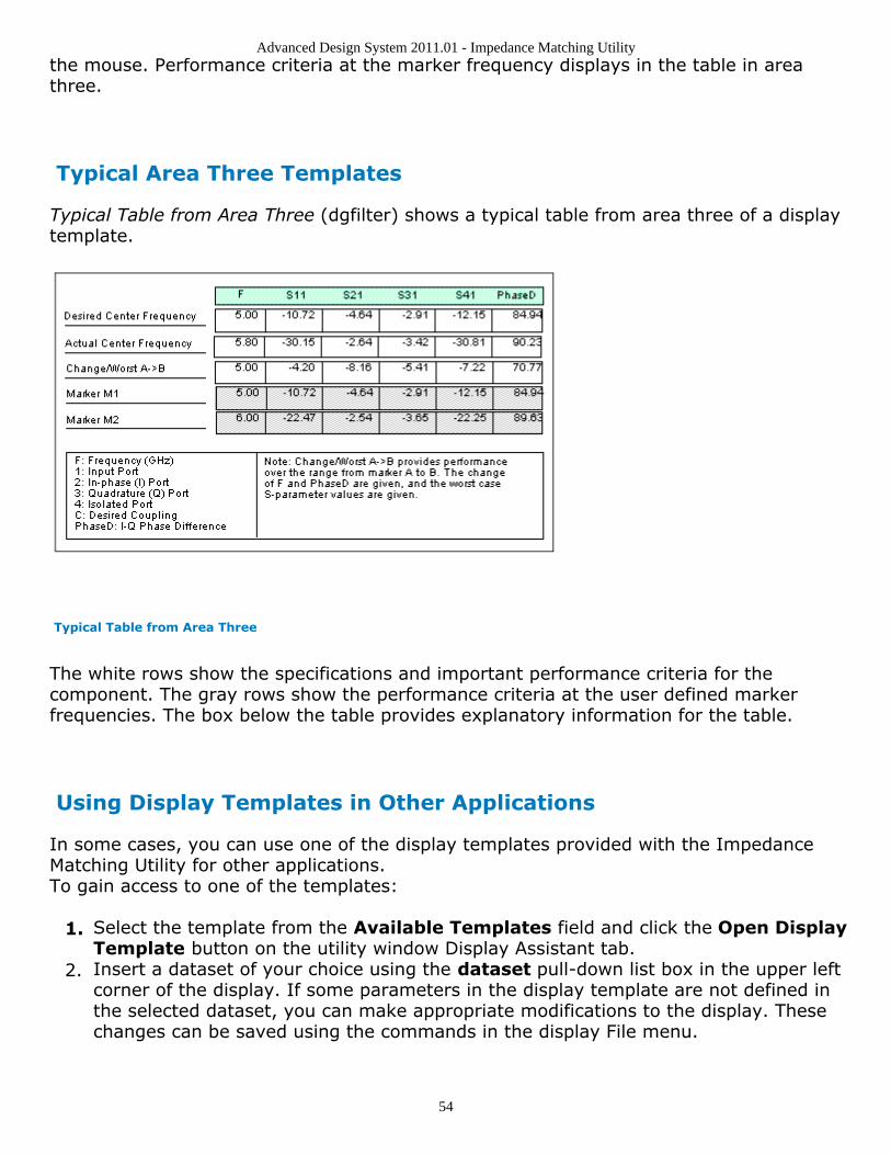
Typical Table from Area Three (dgfilter) shows a typical table from area three of a displaytemplate.
Typical Table from Area Three
The white rows show the specifications and important performance criteria for thecomponent. The gray rows show the performance criteria at the user defined markerfrequencies. The box below the table provides explanatory information for the table.
Using Display Templates in Other Applications
In some cases, you can use one of the display templates provided with the ImpedanceMatching Utility for other applications.To gain access to one of the templates:
Select the template from the Available Templates field and click the Open Display1.Template button on the utility window Display Assistant tab.Insert a dataset of your choice using the dataset pull-down list box in the upper left2.corner of the display. If some parameters in the display template are not defined inthe selected dataset, you can make appropriate modifications to the display. Thesechanges can be saved using the commands in the display File menu.

Advanced Design System 2011.01 - Impedance Matching Utility
55
Transformation Assistant After a Matching Utility SmartComponent has been designed, the lumped inductors andcapacitors can be transformed into equivalent distributed element counterparts using theTransformation Assistant . This feature enables you to quickly and easily transform anideal filter topology to a form that is realizable for high-frequency systems.
Opening the Transformation Assistant
The Transformation Assistant dialog box is accessed from the Matching Utility window,either by selecting Tools > Distributed Element Transformations from the Tools menuor from the Toolbar.
When the Transformation Assistant is opened, the SmartComponent subnetwork appearsin the schematic window and a dialog box is opened. The transformations areaccomplished using the controls on the dialog.

Advanced Design System 2011.01 - Impedance Matching Utility
56
Selecting a Transformation Type
The type of transformation to be applied is selected from three options:
LC to TLine - Transforms lumped inductors and capacitors to ideal transmission lineelements. Eight different inductor/capacitor combinations can be transformed todifferent series lines, series stubs, or shunt stubs.TLine to TLine (Kuroda) - Apply Kuroda's identities in order to transform series shortcircuited stubs to shunt stubs that are realizable in microstrip and other printedtransmission line technologies.LC, TLine to Microstrip - Transforms lumped inductors and capacitors as well as idealtransmission line structures to microstrip equivalent components. Application of thistransformation requires a valid license for the Passive Circuit DesignGuide.After a transform has been selected, the graphical area displays the components thatcan be transformed using the current selection. Black components representelements included in the original circuit available for transformation, while graycomponents represent elements not included in the original circuit. From thisgraphical area, use the left mouse button to select one of the available componenttypes. The graphical area changes to reveal the different distributed elementequivalents available for substitution. Transformations Available for Series InductorCircuit (dgfilter) shows the transformations available when a series inductor circuithas been selected.
Transformations Available for Series Inductor Circuit
Advanced Design System 2011.01 - Impedance Matching Utility
57
From this point, the type of equivalent network can be selected using the left mousebutton from the available structures at the right of the graphics area. A box highlights thecurrently selected structure. Text at the bottom of the window changes as differentselections are made, providing some help concerning the particular transform selected.
Component Selection
After the type of circuit component to be transformed is selected, the actual circuitelements to apply the transform to can be selected using the Component Selection tools.As the left and right arrows within this area are clicked, valid components within theoriginal circuit are highlighted, and their instance names (i.e., L1, C4) appears in the textbox on the Transformation Assistant dialog. The three buttons are used to select whichspecific components should be subject to the current transformation:
Add - Add the currently selected component(s) to the transformation list.Add All - Add all circuit components of the appropriate type to the transformationlist.Cut - Remove the currently selected (highlighted) item in the transformation list fromthe list.
Transformation Buttons
The buttons across the bottom of the dialog box are used to accomplish thetransformation on the selected components.
Transform - Apply the selected transform to the component in the transformationlist.Undo - Undo the last performed transform. This button can be used repeatedly toundo all previous transformations.OK - Accept the current transformed circuit and close the dialog box. After thetransformed circuit has been accepted, transformations cannot be undone.Cancel - Close the dialog box and revert to the original, untransformed circuit.
Changing Component Type
After all transformations have been made on a specific component type (such as seriesinductor), use the left mouse button to click the red return arrow in the upper left handcorner of the graphic area (or use the right mouse button to click anywhere on the graphicarea) to return to the main component selection page. Then you can select anothercomponent type and repeat the transformation steps for this new selection.

Advanced Design System 2011.01 - Impedance Matching Utility
58
Transmission Line Types
Five basic transmission line elements can be produced using the Transformation Assistantare:
Additional Transformation Functions
Unit Element
For certain transformations, either the electrical length or characteristic impedance of theresulting transmission line must be specified by the user. If the Unit Element box ischecked, the resulting transmission line has an electrical length of 45 degrees and thecharacteristic impedance is computed appropriately. If the Unit Element box is unchecked,then the Characteristic Impedance (Z0) box becomes active and the computation uses thischaracteristic impedance to compute the appropriate length.
Characteristic Impedance
The Characteristic Impedance (Z0) box is used to specify the transmission linecharacteristic impedance for certain transformations. In cases where either the electricallength or the characteristic impedance can be specified, this box works in conjunction withthe Unit Element box as discussed above. In certain other cases, this CharacteristicImpedance (Z0) box is used alone. For example, when adding lines to the front or end ofa network as part of Kuroda's identities, the characteristic impedance of the

Advanced Design System 2011.01 - Impedance Matching Utility
59
transformation can be specified using this box.
Adding Transmission Lines
As part of the TLine to TLine transformation, unit element (45 degree electrical length)transmission lines can be added to the front or end of the network. The characteristicimpedance of these lines is specified using the Characteristic Impedance (Z0) box. Suchlines can be added as needed during the transformation process. Addition of these lineschanges the phase response and, if the characteristic impedance is not equal to thenetwork terminal impedance, the magnitude response of the network.
Microstrip Substrate
When performing LC, TLine to MLine transformations, the microstrip substrate thickness(h) and relative permittivity (Er) must be specified. All microstrip elements within a designmust share the same substrate parameters. The substrate parameters used in the finaldesign are the values that appear in the boxes after the final transformation step.
TLine to TLine Transforms (Kuroda Identities)
The TLine to TLine transforms are typically used to transform series short circuited stubsto parallel open circuited stubs in preparation for implementation in planar transmissionline technologies. However, these operations only work on Unit Element lines withelectrical lengths of 45 degrees. Therefore, when performing lumped to ideal distributedtransformations, you must perform substitutions that conform to this Unit Elementspecification. Preferred stubs (highlighted in blue on the graphical area) as well as seriestransmission lines (transformed with the Unit Element box checked) can be transformed inthis way. When adding transmission line elements before or after the network, theelectrical length is 45 degrees and only the characteristic impedance must be specified.
Microstrip Transforms
The LC, TLine to MLine transformations form a somewhat unique class of operations. Thisset of transformations takes lumped inductor/capacitor combinations as well as idealseries transmission lines and shunt transmission line stubs (obtained from the LC to TLinetransformations), and converts them to microstrip. Note that series stubs cannot be usedin this transformation since these cannot be realized in microstrip.
NoteThis set of transforms is only available if a valid license for the Passive Circuit DesignGuide exists.

Advanced Design System 2011.01 - Impedance Matching Utility
60
In addition to the standard transmission line topologies, certain lumped elements can bereplaced with SmartComponents from the Passive Circuit DesignGuide. The availableSmartComponents are:
When making such substitutions, the design capabilities of the Passive Circuit DesignGuideare used to realize the topologies. In this case, however, the design procedure isapproximate, and some tuning of the elements is required before the substituted deviceoffers the correct performance. In such cases, after completion of the transformation,push into the SmartComponent on the schematic window and open the Passive CircuitDesignGuide control window. The Simulation and Optimization Assistants in the PassiveCircuit DesignGuide SmartComponent can then be used to quickly and efficiently tune theperformance of each individual element.

Advanced Design System 2011.01 - Impedance Matching Utility
61
Using SmartComponents in ImpedanceMatching UtilityThis Utility provides several SmartComponents representing matching networks.SmartComponents are smart sub-network designs that provide the container forspecification parameters and a schematic representation of the design when placed into adesign. The utility provides automated design and analysis for these SmartComponents.
Placing and Editing SmartComponentsSmartComponents are placed, copied, edited, and deleted like other components in ADS.The basics of placement, copying, editing, and deleting are described briefly in thissection.
NoteFor more information on ADS basic features see Schematic Capture and Layout (usrguide).
The components are placed in the schematic window by selecting the SmartComponentfrom the palette and clicking at the point where you want to place the component in theschematic.You can display the SmartComponent palette in one of these ways:
Select Tools > Impedance Matching to open the Impedance Matching Utility. Displaythe SmartComponent palette by selecting the Component Palette - All button fromthe utility window toolbar or click View > Component Palette - All from the utilitywindow menu. All contains all of the SmartComponents.Select the Impedance Matching palette from the Component Palette drop-down listbox in the Schematic window toolbar (directly above the palette).
Placing SmartComponents
To place a SmartComponent in the Schematic window:
In the Schematic window, select the component from the SmartComponent palette.1.Click within the schematic window at the location where you want to place the2.SmartComponent.
You can change the orientation of the SmartComponent before placement byselecting from the Insert > Component > Component Orientation commands orby selecting Rotate by -90 repeatedly from the schematic toolbar.The place component mode remains active until you choose End Command fromthe schematic toolbar.
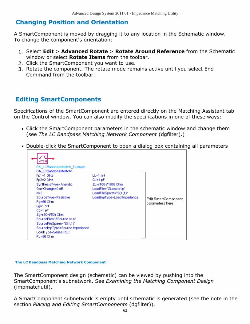
Advanced Design System 2011.01 - Impedance Matching Utility
62
Changing Position and Orientation
A SmartComponent is moved by dragging it to any location in the Schematic window.To change the component's orientation:
Select Edit > Advanced Rotate > Rotate Around Reference from the Schematic1.window or select Rotate Items from the toolbar.Click the SmartComponent you want to use.2.Rotate the component. The rotate mode remains active until you select End3.Command from the toolbar.
Editing SmartComponents
Specifications of the SmartComponent are entered directly on the Matching Assistant tabon the Control window. You can also modify the specifications in one of these ways:
Click the SmartComponent parameters in the schematic window and change them(see The LC Bandpass Matching Network Component (dgfilter).)
Double-click the SmartComponent to open a dialog box containing all parameters
The LC Bandpass Matching Network Component
The SmartComponent design (schematic) can be viewed by pushing into theSmartComponent's subnetwork. See Examining the Matching Component Design(impmatchutil).
A SmartComponent subnetwork is empty until schematic is generated (see the note in thesection Placing and Editing SmartComponents (dgfilter)).
Advanced Design System 2011.01 - Impedance Matching Utility
63
Copying SmartComponentsSmartComponents can be copied within a Schematic or to another Schematic window.
Copying Within a Schematic
To copy a SmartComponent to the same schematic:
Click the SmartComponent to be copied.1.Select Edit > Copy and then Edit > Paste from the schematic window.2.Click where you want the copy placed.3.
Copying Between Schematic Windows
To copy a SmartComponent to another Schematic:
Click the SmartComponent to be copied.1.Select Edit > Copy from the Schematic window.2.Display the schematic window you want to copy the SmartComponent to.3.Select Edit > Paste to copy the SmartComponent to the schematic.4.Click where you want the component placed.5.
Copying a SmartComponent as a Unique Design
Initially, all copied SmartComponents refer to the same SmartComponent design. Whenthe Design Assistant is used to perform a design operation, the Design Assistanttransforms each copied SmartComponent into a unique SmartComponent design. A designoperation is accomplished from the Utility Control Window.
Deleting SmartComponentsSmartComponents can be deleted from a design like other components, but completelyremoving a SmartComponent's files requires the actions described here.
Deleting from Current Schematic Window
Advanced Design System 2011.01 - Impedance Matching Utility
64
Following are the ways to delete a SmartComponent from the schematic window:
Select the component and press the Delete key.Select Delete from the toolbar.Click Edit > Delete from the schematic window.
NoteThis procedure does not remove the SmartComponent files from the workspace directory. To deletefiles from the workspace directory, see Deleting from Current Workspace (dgfilter).
Deleting from Current Workspace
To delete a SmartComponent and all associated files from your workspace:
In the Schematic window, select the SmartComponent.1.In the utility window, select Tools > Delete SmartComponent. or on the toolbar,2.click Delete . This deletes the SmartComponent from the current schematic andremoves all of its files from your workspace. The SmartComponent delete moderemains active until you select End Command from the schematic toolbar.
Deleting Manually Using File System
You can use your computer's file system to delete a SmartComponent by deleting theappropriate files in the network subdirectory of a workspace. Delete files that start withDA_ or SA_ , contain the SmartComponent title, and end with . ael, .atf, or .wrk.
Using SmartComponents as Standalone ComponentsAfter SmartComponents are designed and tested, they can be used as standalonecomponents. The Matching Utility is not needed to use them in new schematic unless youwish to modify or analyze them. When using the SmartComponent in a schematic,however, the power supply pins (Vdd, Vcc, Vp, Vm) must be connected to a DC voltagesource whose voltage level corresponds the parameter setting.
Using an Existing SmartComponent Within the Same Workspace
To use an existing SmartComponent within the same workspace:
Open the Component Library window by selecting Insert > Component >1.Component Library from the Schematic window or Display Component Library

Advanced Design System 2011.01 - Impedance Matching Utility
65
List on the toolbar.Select the Library name under All Libraries list at the left of the Component Library2.window. Available components are listed in the Components list at the right of theComponent Library window.Select the SmartComponent in the Components list.3.Place the SmartComponent into your schematic by clicking in the Schematic window4.at the location you wish to place. The insert mode remains active until you click EndCommand.
Using an Existing SmartComponent in Any Workspace
A library of predesigned reusable SmartComponents can be created by placing thereusable SmartComponents in a workspace. This workspace can be included in anyworkspace and its SmartComponents can be accessed using the Component Library.
To use an existing SmartComponent in any workspace:
Open the Workspace where the SmartComponent needs to be inserted.1.Open the Library in the Workspace by selecting File > Open > Library.2.Open the Component Library window by selecting Insert > Component >3.Component Library from the Schematic window or Display Component LibraryList from the toolbar.Select the Library name under All Libraries list at the left of the Component Library4.window. Available components are listed in the Components list at the right of theComponent Library window.Select the SmartComponent in the Components list.5.Place the SmartComponent into your schematic by clicking in the Schematic window6.at the location where you wish to place the component. The insert mode remainsactive until you click End Command.


