Embed Size (px)
Citation preview
IMPACT OF GEOMETRICAL ASPECT RATIO ON THE
PERFORMANCE OF PHASE CHANGE MEMORY DEVICES
A PROJECT REPORT
submitted by
K C CHANDINI DEVI
(EE19M046)
Submitted in partial fulfilment of the requirements for the award of the degree
of
MASTER OF TECHNOLOGY
In
MICROELECTRONICS AND VLSI DESIGN
DEPARTMENT OF ELECTRICAL ENGINEERING
INDIAN INSTITUTE OF TECHNOLOGY MADRAS
CHENNAI-600036
JUNE 2021
CERTIFICATE
This is to certify that the project titled “Impact of Geometrical Aspect Ratio on the Performance
of Phase Change Memory Devices” being submitted to the Indian Institute of Technology Madras
by K C Chandini Devi (EE19M046), in partial fulfilment of the requirements for the award of the
degree of Master of Technology in Microelectronics and VLSI design in Electrical Engineering is
a Bonafide record of work carried out by her under my supervision. The contents of this project report,
in full or in parts, have not been submitted to any other institute or university for the award of any
degree or diploma.
Dr Anbarasu Manivannan Prof. Ravinder David Koilpillai
Project Guide Head of the Department
Associate Professor Professor
Dept. of Electrical Engineering Dept. of Electrical Engineering
Indian Institute of Technology, Madras Indian Institute of Technology, Madras
Place: Chennai
Date: 17-06-2021

1
ACKNOWLEDGEMENT
I would like to express my deep sense of gratitude to my project guide Dr Anbarasu Manivannan for
his valuable guidance, support and encouragement throughout the period of the project work. I would
also like to thank Suresh Durai for giving me valuable suggestions, motivation and insights throughout
the project. I also like to offer my thanks to my lab mates (Ms. Sudha Kumari, Mr. Sakthi Kumaran,
Mr. Salman Khan) who provided constant help when required. I am highly indebted to them for
devoting their valuable time. I sincerely thank them for the help and motivation they provided in order
to execute this work in good time.

2
ABSTRACT
In nano-scale device architecture, it is ideally difficult to fabricate devices with circular cross-section.
Due to limited controllability in manufacturing process, devices end up with elliptical cross-section
instead of circular cross-section. This is defined by a geometrical parameter called aspect ratio (AR)
which is given by the ratio of length of major axis to that of minor axis. The devices with different AR
results in different area and in specific the variations in the area of heater and pore found in the
cylindrical type PCM device architectures like mushroom and pore-type could affect the programming
of the device and result in performance degradation.
In this thesis work, the impact of geometrical variation in circular cross-section of mushroom-
type and pore-type PCM devices (including scaled-down devices) have been investigated and their
results have been compared to understand which of these devices are least sensitive to variation in
circular cross-section.

3
CONTENTS
ACKNOWLEDGEMENT 1
ABSTRACT 2
LIST OF FIGURES 5
LIST OF TABLES 8
1. INTRODUCTION
1.1 Need for new memory technology 9
1.2 Emerging memory technologies 10
1.2.1 Storage class memory 10
1.2.2 Characteristics of EM technology 11
1.2.3 Candidates for EM technologies 11
1.2.4 Comparison of EM technology with conventional memory 14
1.3 Phase change memory 15
1.3.1 Material composition 15
1.3.2 Working principle 16
1.3.3 Electrical I-V characteristics of PCM 17
1.3.4 Basic PCM device architecture- merits and demerits 18
1.3.5 Interfacial effects 19
1.3.6 Past, present and future applications of PCM 20
1.4 Process variation 24
1.4.1 Geometrical Aspect Ratio (AR) 25
1.5 Objective of thesis 26
2. SIMULATION METHODOLOGY
2.1 Introduction 27
2.2 Sentaurus TCAD 27
2.2.1 Sentaurus Structure Editor 28
2.2.2 Sentaurus Device (SDEVICE) 28
2.2.3 Sentaurus Visual (SVISUAL) 31

4
2.2.4 Inspect 31
2.3 Interconnection the models for PCM device calibration 31
2.4 Summary 33
3. IMPACT OF GEOMETRICAL ASPECT RATIO ON THE PERFORMANCE OF
MUSHROOM-TYPE PCM DEVICE
3.1 Introduction 34
3.2 Device structure of mushroom-type PCM 35
3.3 Simulation method 36
3.4 Results and discussion 37
4. IMPACT OF GEOMETRICAL ASPECT RATIO ON THE PERFORMANCE OF PORE-
TYPE PCM DEVICE
4.1 Device structure and simulation methodology 44
4.2 Results and discussion 45
4.3 Comparison of impact of AR on reset operation between mushroom-type and pore-type 48
5. CONCLUSION 50
References 51
5
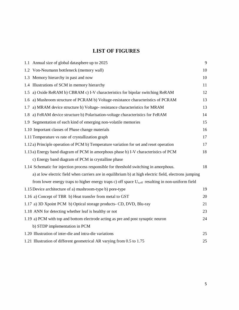
LIST OF FIGURES
1.1 Annual size of global datasphere up to 2025 9
1.2 Von-Neumann bottleneck (memory wall) 10
1.3 Memory hierarchy in past and now 10
1.4 Illustrations of SCM in memory hierarchy 11
1.5 a) Oxide ReRAM b) CBRAM c) I-V characteristics for bipolar switching ReRAM 12
1.6 a) Mushroom structure of PCRAM b) Voltage-resistance characteristics of PCRAM 13
1.7 a) MRAM device structure b) Voltage- resistance characteristics for MRAM 13
1.8 a) FeRAM device structure b) Polarisation-voltage characteristics for FeRAM 14
1.9 Segmentation of each kind of emerging non-volatile memories 15
1.10 Important classes of Phase change materials 16
1.11 Temperature vs rate of crystallization graph 17
1.12 a) Principle operation of PCM b) Temperature variation for set and reset operation 17
1.13 a) Energy band diagram of PCM in amorphous phase b) I-V characteristics of PCM 18
c) Energy band diagram of PCM in crystalline phase
1.14 Schematic for injection process responsible for threshold switching in amorphous. 18
a) at low electric field when carriers are in equilibrium b) at high electric field, electrons jumping
from lower energy traps to higher energy traps c) off space Ua,off resulting in non-uniform field
1.15 Device architecture of a) mushroom-type b) pore-type 19
1.16 a) Concept of TBR b) Heat transfer from metal to GST 20
1.17 a) 3D Xpoint PCM b) Optical storage products- CD, DVD, Blu-ray 21
1.18 ANN for detecting whether leaf is healthy or not 23
1.19 a) PCM with top and bottom electrode acting as pre and post synaptic neuron 24
b) STDP implementation in PCM
1.20 Illustration of inter-die and intra-die variations 25
1.21 Illustration of different geometrical AR varying from 0.5 to 1.75 25

6
2.1 Sentaurus Device tool flow 29
2.2 Interconnection of models for PCM device simulation. V, ρ, J and T represent electric 33
potential, charge density, current density and temperature
3.1 2D schematic of mushroom-type pcm device along with their dimensions for heater radius 35
of a) 50nm b)10nm
3.2 TCAD generated 3D cylindrical mushroom type pcm with circular cross-section after 36
removing oxide and tungsten.
3.3 R-I characteristics for nominal case (AR=1) for heater diameter of a) 100nm b)20nm 37
3.4 a) Reset current values for AR varying from 0.5 to 1.75 for heater diameter of 100nm 39
b) Reset resistance values for AR varying from 0.5 to 1.75 for heater diameter of 100nm
c) Maximum lattice temperature obtained for AR varying from 0.5 to 1.75 for heater
diameter of 100nm for nominal reset current value of 1.5mA d) Current density values
for AR varying from 0.5 to 1.75 for heater diameter of 100nm
3.5 a) Reset current values for AR of heater varying from 0.5 to 1.75 for scaled down 40
device for heater diameter 20nm b) Reset resistance values for AR of heater varying
from 0.5 to 1.75 for 20nm c) Maximum lattice temperature obtained for AR of heater
varying from 0.5 to 1.75 for 20nm for nominal reset current value of 220µA
d) Current density values for AR of heater varying from 0.5 to 1.75 for 20nm
3.6 Comparison of percentage change in reset current for heater diameter of 100nm and 20nm 41
3.7 a) Reset current values for AR of GST varying from 0.5 to 1.75 for heater diameter 42
100nm b) Reset resistance values for AR of GST varying from 0.5 to 1.75 for 100nm
c) Reset current values for AR of GST varying from 0.5 to 1.75 for scaled down device
for heater diameter 20nm d) Reset resistance values for AR of GST varying from 0.5 to 1.75
for 20nm
3.8 Comparison of percentage change in reset current for heater diameter of 100nm and 20nm 43
4.1 TCAD generated pore type device structure with circular cross section (oxide is removed) 44
4.2 R-I characteristics for nominal case (AR=1) in a) 100nm b)20nm 45
4.3 a) Reset current values for AR varying from 0.5 to 1.75 for pore diameter of 100nm 46
b)Rreset resistance values for AR varying from 0.5 to 1.75 for pore diameter of 100nm
c) Maximum lattice temperature obtained for AR varying from 0.5 to 1.75 for 100nm pore
diameter of 100nm for nominal reset current value of 1.1mA d) Current density values
for AR varying from 0.5 to 1.75 for pore diameter of 100nm
4.4 a) Reset current values for AR varying from 0.5 to 1.75 for pore diameter of 20nm 47
b) Reset resistance values for AR varying from 0.5 to 1.75 for pore diameter of 20nm

7
c) Maximum lattice temperature obtained for AR varying from 0.5 to 1.75 for 20nm
pore diameter of 100nm for nominal reset current value of 120µA d) Current density
values for AR varying from 0.5 to 1.75 for pore diameter of 20nm
4.5 Comparison of percentage change in reset current for pore diameter of 100nm and 20nm 48
4.6 Comparison of percentage change in reset current with pore and heater AR for 49
a) 100nm b) 20nm

8
LIST OF TABLES
1.1 Comparison of performance metrics between mainstream memories and emerging memories 14
2.1 Thermal parameters used for the PCM device simulation 32
3.1 Reset current and resistance values for heater diameter of 100nm 43
3.2 Reset current and resistance values for heater diameter of 20nm 43

9
CHAPTER 1
INTRODUCTION
1.1 Need for new memory technology
Today, digitalization is almost unavoidable in everyone’s life. It generates huge amount of digital
data all over the world and to outpace this ever-increasing rate of global data, the capacities of current
mass storage devices need to be increased tremendously [1]. However, today’s conventional storage
device like Hard disk drive and silicon-based memory devices like SRAM, DRAM and flash memory
are reaching their physical limits and thereby further enhancement in the data storage by using the
existing memory technologies becomes challenging. Also, the future requirements of data storage are
in the range of ZB. In a paper released by international data corporation (IDC) in 2018 [2], the global
data requirement was predicted to be 175ZB in 2025 as shown in fig1.1.
Fig1.1 Annual size of global datasphere up to 2025 [2]
On the other hand, the processor speed is restricted by Von-Neumann bottleneck. In
conventional Von-Neumann based computer architecture, programs and data are stored in memory.
The processor and memory units are separated physically and the data needs to be shuffled frequently
between these two units. Since the memory cannot keep up with the processor speed, the processor
remains idle for a certain amount of time waiting for data to be fetched from memory. Also, moving
the data back and forth, as a memory access consumes 100 to 1000 times more energy than a CPU
operation. One way to solve this problem is to have a memory device that can not only store data but
can also perform computational tasks i.e., in-memory computation and addition it should be a fast
access, less energy consumable memory device.

10
Fig1.2 Von-Neumann bottleneck (memory wall) [3]
Thus, to keep up with the massive demand of data storage and for future applications like in-
memory computing, a new memory technology is necessary which is scalable, low power, fast data
access and perform in-memory computational tasks.
1.2 Emerging memory (EM) technologies
1.2.1 Storage class memory (SCM)
Fig1.3 Memory hierarchy in past and now [47]
SRAM, DRAM and flash memory are the main stream memory technologies serving as cache,
main memory and storage memory. In the memory hierarchy, towards cache, memory read/write
latency decreases and moving down the memory hierarchy towards storage (NAND, HDD), the
memory capacity decreases. When compared to flash, SRAM and DRAM has lower latency but they
are volatile in nature i.e., data is lost when power is off. Hence, they cannot be used as storage memory
but can be used as working memory due to its lower latency. On the other hand, flash has poor latency
but non-volatile in nature i.e., the data is retained even when power is off. Hence, it is used as storage
memory due to its longer data retention.
As shown in fig1.3 there are two performance gaps in memory hierarchy [4]. One gap is
between SRAM and DRAM. This is caused by the bottleneck of DRAM speed. Owing to its working
principle, DRAM cannot operate as fast as SRAM. The other performance gap is between DRAM and
NAND flash which usually takes µs-ms to write and read the data. The gap between SRAM and

11
DRAM can be filled by embedded DRAM. Besides, to fill the huge gap between DRAM and NAND
flash memory, there is desperate need for EM which can serve as a SCM whose performance lies
between NAND and DRAM in terms of latency and density metrics. This SCM can serve in two ways
(fig1.4), one as storage type to replace NAND, which primarily requires high-density and low-power
and other as a memory-type SCM, to replace DRAM, which requires mostly fast access time and high
endurance.
Fig1.4 Illustrations of SCM in memory hierarchy [5]
1.2.2 Characteristics of EM technology
All the silicon-based memories like SRAM, DRAM and flash memory are charge based
storage devices. SRAM stores the charge at storage nodes of two cross coupled inverters, whereas
DRAM stores the charge at cell capacitor and flash memory stores charge at floating gate of transistor.
When all these charge-based storage devices scaled down, the liability in storing charge becomes
questionable resulting in performance degradation, reliability and noise margin. Therefore, it would
be better to have the programming of the EM technologies to be non-charge based storage. The ideal
characteristics for any EM technology include [6]
Non volatility
Fast Read/write access(<1ns)
Excellent scalability(<10nm)
Low power consumption(<pw)
High endurance (>1017)
Long data retention (>10 years)
Low cost per bit
1.2.3 Candidates for Emerging memory technologies
Several emerging NVM have been pursued to achieve the above-mentioned ideal
characteristics. Nevertheless, it is impossible to have a memory technology satisfying all the ideal

12
characteristics. Some of the potential candidates for emerging memory technology are ReRAM,
PCRAM, FeRAM and MRAM.
a) ReRAM: referred as resistive RAM or RRAM. The structure consists of a dielectric sandwiched
between two metal electrodes. By changing the resistance between two electrodes, the data can be
stored as either 1 or 0. There are two subcategories: one is oxide RAM and the other is conductive
bridge RAM (CBRAM). The operating principle of both utilises redox operation hence the name redox
RAM (ReRAM). By applying a high voltage pulse, filaments are formed by knocking the oxygen
atoms out of lattice giving 𝑂2− ions which are now free to move towards anode (+) in oxide RAM. In
case of CBRAM filaments are formed by movement of metal atom. This operation is called set
operation and applying a read voltage, the device shows low resistance state. For the reset operation,
the oxygen ions recombine or metal atoms dissociate giving rise to high resistance state. The switching
mechanism here can be either unipolar or bipolar. The unipolar mode requires large write current and
show less endurance. Thus bipolar switching is preferred over unipolar [6].
(a) (b) (c)
Fig1.5 a) Oxide ReRAM b) CBRAM c) I-V characteristics for bipolar switching ReRAM
b) PCRAM: As in ReRAM, PCRAM also stores data by change in material resistance. The structure
consists of chalcogenide-based phase change material sandwiched between two electrodes. By
switching the material rapidly and reversibly from crystalline to amorphous, the resistance of the
material is altered from low to high or vice-versa. Switching the material from crystalline to
amorphous is called reset operation and this can be achieved by applying a high amplitude voltage or
current pulse for a short amount of time (tens of ns). On the other hand, switching the material from
amorphous to crystalline is called set operation and this can be achieved by applying a short amplitude
voltage or current pulse for a longer duration (hundreds of ns). Thus, a change in the phase of material
results in the change in the resistance state. This change in resistance value can be stored as logic 1 or
logic 0. The typical PCRAM structure (mushroom type) and its characteristics are shown in figure 1.6

13
(a) (b)
Fig1.6 a) Mushroom structure of PCRAM b) Voltage-resistance characteristics of PCRAM [7]
c) MRAM: Like HDD, MRAM also uses magnetic state to store information but unlike HDD, MRAM
can read and write electrically and does not have any moving parts. The structure consists of two
ferromagnetic materials with non-magnetic materials (tunnel barrier) in between them. Out of two
ferromagnetic material one is pinned with fixed magnetic polarisation and the other is free layer where
the magnetic polarisation can be switched in either direction. Switching in free layer leads to two
polarisation states: parallel (P) and antiparallel (AP) state. Switching the material from AP to P state
is called set transition which gives low resistance state as both have same polarisation, majority
electrons go un-scattered and minority electrons gets scattered. Switching the material from P to AP
state is called reset transition which gives high resistance state. Since both layers have different
polarisation majority electrons gets scattered and minority electrons go un-scattered. Thus, by
changing the polarisation, we can change the resistance state. This change in resistance value can be
stored as logic 1 or 0.
(a) (b)
Fig1.7 a) MRAM device structure b) Voltage- resistance characteristics for MRAM [7]
d) FeRAM: The structure consists of ferroelectric layer sandwiched between two metal electrodes.
This ferroelectric layer is used as a capacitor for storing data. By orientation of polarisation, the data
can be stored as either logic 1 or 0. The polarization-voltage characteristic of FERAM is shown in
figure 1.8 (b). By applying the positive voltage sweep to the device leads to a permanent polarization
(+Pr) of electric dipole in the FE layer, while applying a negative voltage sweep causes another
permanent polarization (-Pr). A transient displacement current is observed to confirm the polarization

14
switching in FE layer. Thus, by changing the polarisation from +Pr to -Pr or from -Pr to +Pr, the data
can be stored as 1 or 0. Besides, FERAM does not show any change in the resistance value and hence,
cannot be used as a resistive memory as compared to other EM technologies.
(a) (b)
Fig1.8 a) FeRAM device structure b) Polarisation-voltage characteristics for FeRAM [7]
1.2.4 Comparison of emerging memory technology with conventional
memory
The table below lists the key parameters of each type of new RAM technologies and compares
them with typical mainstream memories. (NA-not available, y-years)
Table 1.1 Comparison of performance metrics between mainstream memories and emerging memories [6]
Mainstream memories Emerging memories
parameters SRAM DRAM NOR NAND ReRAM PCRAM MRAM FeRAM
Cell size >100F2 6F2 10F2 <4F2 4-12F2 4-30F2 6-50F2 15-34F2
Multi bit 1 1 2 3 2 2 1 1
Voltage (V) <1 <1 >10 >10 <3 <3 <1.5 <4
Read time ~1ns ~10ns ~50ns ~10µs <10ns <10ns <10ns <10ns
Write time ~1ns ~10ns 10µs-
1ms
100µs-
1ms
<10ns ~50ns 1-10ns ~30ns
Write energy(/bit)
~fJ ~10fJ ~100pJ ~10fJ 0.1-1pJ 10pJ ~0.1pJ ~0.1pJ
Retention NA ~64ms >10y >10y >10y >10y >10y >10y
Endurance >1016 >1016 105 105 106-1012 109 1015 1010
Scalability Yes yes yes yes moderate yes no no
From the table, can be observed that among all the memory technologies, SRAM still stands
close to processing core as L1 cache in memory hierarchy due to its fast access, low energy
consumption and scalability. On the other hand, MRAM can replace L2/L3 SRAM cache as a non-
volatile working memory as it has lower latency and longer endurance making it a suitable candidate
for replacement of L2/L3 SRAM cache [4]. Although MRAM has the advantage of lower latency and
longer endurance, it suffers from BEOL thermal budget and scalability problems. FeRAM has an
advantage of easy embedding into LSI logic circuits and high-speed operation, but it faces problems
15
like reliability and scalability problems and also further research needs to be done on FeRAM. And
as a storage class memory, two emerging memory can be used ReRAM and PCRAM. ReRAM has
advantage of low cost and high density but has reliability issues and low cycling endurance. And
PCRAM suggests to be a matured memory technology due to its improved process and manufacturing
developments. Also, PCRAM has superior features like high scalability, MLC capability for high
density. Nevertheless, the key challenges in PCM are consumption of high reset current and longer
crystallization time. By reducing reset current, PCM can be made more suitable candidate for SCM
applications.
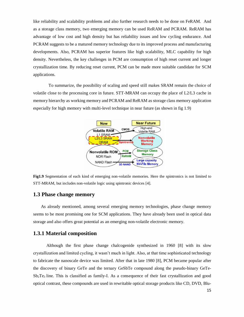
To summarize, the possibility of scaling and speed still makes SRAM remain the choice of
volatile close to the processing core in future. STT-MRAM can occupy the place of L2/L3 cache in
memory hierarchy as working memory and PCRAM and ReRAM as storage class memory application
especially for high memory with multi-level technique in near future (as shown in fig 1.9)
Fig1.9 Segmentation of each kind of emerging non-volatile memories. Here the spintronics is not limited to
STT-MRAM, but includes non-volatile logic using spintronic devices [4].
1.3 Phase change memory
As already mentioned, among several emerging memory technologies, phase change memory
seems to be most promising one for SCM applications. They have already been used in optical data
storage and also offers great potential as an emerging non-volatile electronic memory.
1.3.1 Material composition
Although the first phase change chalcogenide synthesized in 1960 [8] with its slow
crystallization and limited cycling, it wasn’t much in light. Also, at that time sophisticated technology
to fabricate the nanoscale device was limited. After that in late 1980 [8], PCM became popular after
the discovery of binary GeTe and the ternary GeSbTe compound along the pseudo-binary GeTe-
Sb2Te3 line. This is classified as family-I. As a consequence of their fast crystallization and good
optical contrast, these compounds are used in rewritable optical storage products like CD, DVD, Blu-
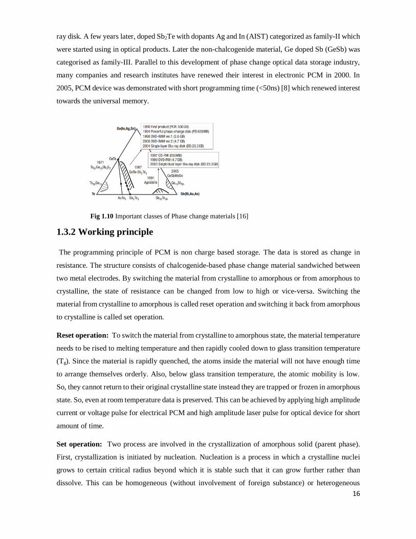
16
ray disk. A few years later, doped Sb2Te with dopants Ag and In (AIST) categorized as family-II which
were started using in optical products. Later the non-chalcogenide material, Ge doped Sb (GeSb) was
categorised as family-III. Parallel to this development of phase change optical data storage industry,
many companies and research institutes have renewed their interest in electronic PCM in 2000. In
2005, PCM device was demonstrated with short programming time (<50ns) [8] which renewed interest
towards the universal memory.
Fig 1.10 Important classes of Phase change materials [16]
1.3.2 Working principle
The programming principle of PCM is non charge based storage. The data is stored as change in
resistance. The structure consists of chalcogenide-based phase change material sandwiched between
two metal electrodes. By switching the material from crystalline to amorphous or from amorphous to
crystalline, the state of resistance can be changed from low to high or vice-versa. Switching the
material from crystalline to amorphous is called reset operation and switching it back from amorphous
to crystalline is called set operation.
Reset operation: To switch the material from crystalline to amorphous state, the material temperature
needs to be rised to melting temperature and then rapidly cooled down to glass transition temperature
(Tg). Since the material is rapidly quenched, the atoms inside the material will not have enough time
to arrange themselves orderly. Also, below glass transition temperature, the atomic mobility is low.
So, they cannot return to their original crystalline state instead they are trapped or frozen in amorphous
state. So, even at room temperature data is preserved. This can be achieved by applying high amplitude
current or voltage pulse for electrical PCM and high amplitude laser pulse for optical device for short
amount of time.
Set operation: Two process are involved in the crystallization of amorphous solid (parent phase).
First, crystallization is initiated by nucleation. Nucleation is a process in which a crystalline nuclei
grows to certain critical radius beyond which it is stable such that it can grow further rather than
dissolve. This can be homogeneous (without involvement of foreign substance) or heterogeneous

17
(parent phase is in contact with foreign substance which will act as nucleation site). After stable crystal
cluster is formed, they will grow to macroscopic size which is nothing but crystal growth. To switch
the material from amorphous to crystalline, we need to rise the material temperature between Tm and
Tg where we can get high crystallization speed. Above Tm, although atomic mobility is more the
driving force for crystallization is low. So, crystallization process will be slow. At below Tg, although
driving force for crystallization is more, atomic mobility is less. Therefore, again crystallization
process will be slow. Thus, (from fig 1.11) highest crystallization speed can be observed between Tm
and Tg where there is a good compromise between driving force and mobility.
. Fig 1.11 Temperature vs rate of crystallization graph
The set and reset operation in typical mushroom type cell is as shown in fig 1.12
Fig 1.12 a) Principle operation of PCM b) Temperature variation for set and reset operation [9]
1.3.3 Electrical I-V characteristics of PCM
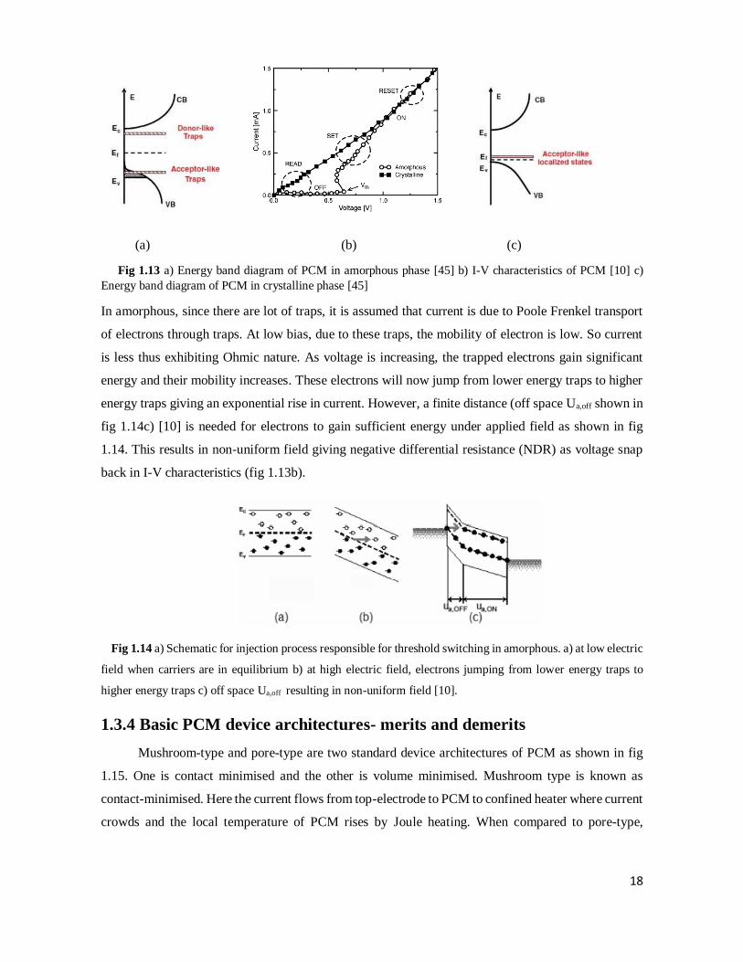
In crystalline phase, the device acts like a p-type semiconductor as shown in energy band
diagram (fig 1.13c). so, the I-V characteristics of PCM in crystalline phase shows Ohmic nature. In
amorphous, the I-V characteristic is Ohmic for low voltages and exponential for high voltages.
18
(a) (b) (c)
Fig 1.13 a) Energy band diagram of PCM in amorphous phase [45] b) I-V characteristics of PCM [10] c)
Energy band diagram of PCM in crystalline phase [45]
In amorphous, since there are lot of traps, it is assumed that current is due to Poole Frenkel transport
of electrons through traps. At low bias, due to these traps, the mobility of electron is low. So current
is less thus exhibiting Ohmic nature. As voltage is increasing, the trapped electrons gain significant
energy and their mobility increases. These electrons will now jump from lower energy traps to higher
energy traps giving an exponential rise in current. However, a finite distance (off space Ua,off shown in
fig 1.14c) [10] is needed for electrons to gain sufficient energy under applied field as shown in fig
1.14. This results in non-uniform field giving negative differential resistance (NDR) as voltage snap
back in I-V characteristics (fig 1.13b).
Fig 1.14 a) Schematic for injection process responsible for threshold switching in amorphous. a) at low electric
field when carriers are in equilibrium b) at high electric field, electrons jumping from lower energy traps to
higher energy traps c) off space Ua,off resulting in non-uniform field [10].
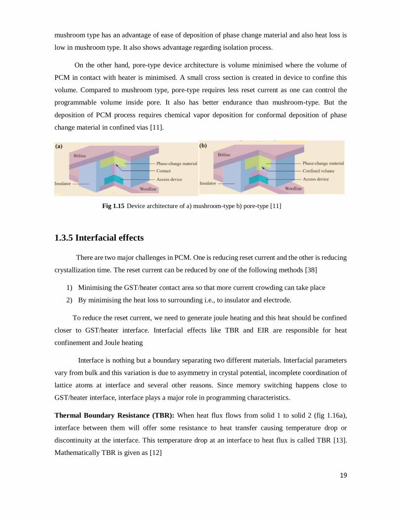
1.3.4 Basic PCM device architectures- merits and demerits
Mushroom-type and pore-type are two standard device architectures of PCM as shown in fig
1.15. One is contact minimised and the other is volume minimised. Mushroom type is known as
contact-minimised. Here the current flows from top-electrode to PCM to confined heater where current
crowds and the local temperature of PCM rises by Joule heating. When compared to pore-type,
19
mushroom type has an advantage of ease of deposition of phase change material and also heat loss is
low in mushroom type. It also shows advantage regarding isolation process.
On the other hand, pore-type device architecture is volume minimised where the volume of
PCM in contact with heater is minimised. A small cross section is created in device to confine this
volume. Compared to mushroom type, pore-type requires less reset current as one can control the
programmable volume inside pore. It also has better endurance than mushroom-type. But the
deposition of PCM process requires chemical vapor deposition for conformal deposition of phase
change material in confined vias [11].
Fig 1.15 Device architecture of a) mushroom-type b) pore-type [11]
1.3.5 Interfacial effects
There are two major challenges in PCM. One is reducing reset current and the other is reducing
crystallization time. The reset current can be reduced by one of the following methods [38]
1) Minimising the GST/heater contact area so that more current crowding can take place
2) By minimising the heat loss to surrounding i.e., to insulator and electrode.
To reduce the reset current, we need to generate joule heating and this heat should be confined
closer to GST/heater interface. Interfacial effects like TBR and EIR are responsible for heat
confinement and Joule heating
Interface is nothing but a boundary separating two different materials. Interfacial parameters
vary from bulk and this variation is due to asymmetry in crystal potential, incomplete coordination of
lattice atoms at interface and several other reasons. Since memory switching happens close to
GST/heater interface, interface plays a major role in programming characteristics.
Thermal Boundary Resistance (TBR): When heat flux flows from solid 1 to solid 2 (fig 1.16a),
interface between them will offer some resistance to heat transfer causing temperature drop or
discontinuity at the interface. This temperature drop at an interface to heat flux is called TBR [13].
Mathematically TBR is given as [12]

20
Rd,th = 𝑇
SL (1.1)
Where T is temperature drop across the interface. SL is heat flux and Rd,th is TBR. The
physical phenomenon responsible for TBR is electron-phonon interactions close to GST/heater
interface. Heat transfer takes place through electron at metal and through phonon at PCM. At interface,
energy transfer from electrons to ions via electron-phonon coupling to allow phonons to transfer heat
across the junction [14].
Fig 1.16 a) Concept of TBR [13] b) Heat transfer from metal to GST [14]
Electrical Interface Resistance (EIR): EIR is just a contact resistance between GST/heater which
primarily depends on barrier height between GST and heater. EIR is responsible for efficient Joule
heating given by [15]
HJ =𝐽^2
𝜎 (1.2)
Where HJ is Joule heat, J is current density and 𝜎 is electrical conductivity. Higher value of
contact resistance can reduce resistance window and disturbs read operation in PCM devices. So, we
should choose proper TBR and EIR values such that they don’t reduce the resistance window.
1.3.6 Past, present and future applications of PCM
Past application: optical storage disc
PCM are used in rewritable optical storage like CD, DVD, blue-ray disc. By applying short and high
amplitude laser pulse or long and low amplitude pulse, logic 1 or 0 can be written. The storage is
achieved by modulating the reflectivity and the state of the cell can be read by applying weak laser
pulse.
Present application: selectors
Memory switching of PCM requires high reset current and this current is supplied to memory device
by selectors. So, the selector should be able to provide high current. Usually, MOSFET transistors are
21
used as selectors. In MOSFET, I α (𝑊
𝐿). So, to increase the current (
𝑊
𝐿) ratio should be increased. Also,
MOSFET is a 3 terminal device making it bulky. So, a two terminal selector device is required which
can occupy less space. One such device chalcogenide (Te and Se) based selectors. PCM can be used
as selectors by switching the device from a-off (high resistance) to a-on (low resistance) (as shown in
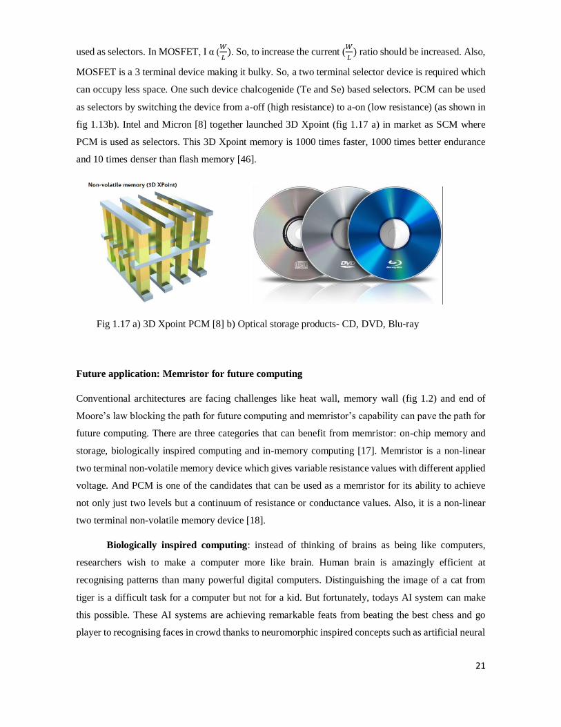
fig 1.13b). Intel and Micron [8] together launched 3D Xpoint (fig 1.17 a) in market as SCM where
PCM is used as selectors. This 3D Xpoint memory is 1000 times faster, 1000 times better endurance
and 10 times denser than flash memory [46].
Fig 1.17 a) 3D Xpoint PCM [8] b) Optical storage products- CD, DVD, Blu-ray
Future application: Memristor for future computing
Conventional architectures are facing challenges like heat wall, memory wall (fig 1.2) and end of
Moore’s law blocking the path for future computing and memristor’s capability can pave the path for
future computing. There are three categories that can benefit from memristor: on-chip memory and
storage, biologically inspired computing and in-memory computing [17]. Memristor is a non-linear
two terminal non-volatile memory device which gives variable resistance values with different applied
voltage. And PCM is one of the candidates that can be used as a memristor for its ability to achieve
not only just two levels but a continuum of resistance or conductance values. Also, it is a non-linear
two terminal non-volatile memory device [18].
Biologically inspired computing: instead of thinking of brains as being like computers,
researchers wish to make a computer more like brain. Human brain is amazingly efficient at
recognising patterns than many powerful digital computers. Distinguishing the image of a cat from
tiger is a difficult task for a computer but not for a kid. But fortunately, todays AI system can make
this possible. These AI systems are achieving remarkable feats from beating the best chess and go
player to recognising faces in crowd thanks to neuromorphic inspired concepts such as artificial neural

22
network (ANN) [19]. Before looking at ANN, lets see how our brain works and where we can use
these memristors.
Our brain consists of lot of neurons and synapses. A neuron is made up of a soma, an axon and
dendrites. Soma takes up the majority of neuron and it is connected through neighbouring neurons
through axons and dendrites. Axons acts like output. It transmits signal and dendrites receives signals
from neighbouring neuron. The gap between axons of previous neuron and dendrites of next neuron
is called synapse and the connection strength between these two neighbouring neurons are called
synaptic weight. This synaptic weight can be potentiated (strengthened) or depressed (weakened) by
a process called synaptic plasticity. Synaptic plasticity is categorised into short term plasticity (where
change lasts for short time) and long-term plasticity (change lasts for long time). Long-time synaptic
plasticity (LTSP) is what responsible for our learning and memory. This is again classified as long-
term potentiation (LTP) and long-term depression (LTD). In long term potentiation, synaptic weight
is strengthened for long term memory and in long term depression, synaptic weight is weakened.
LTSP can be explained by mechanism called spike time dependent plasticity (STDP). The synaptic
weight can be increased or decreased by spiking time difference between pre synaptic and post
synaptic neuron. If pre synaptic spike precedes post synaptic spike, it leads to LTP and if pre synaptic
spike lags behind post synaptic spike, it leads to LTD. We can use the same mechanism (STDP) in
pcm to control synaptic weights which will be shown as resistance values.
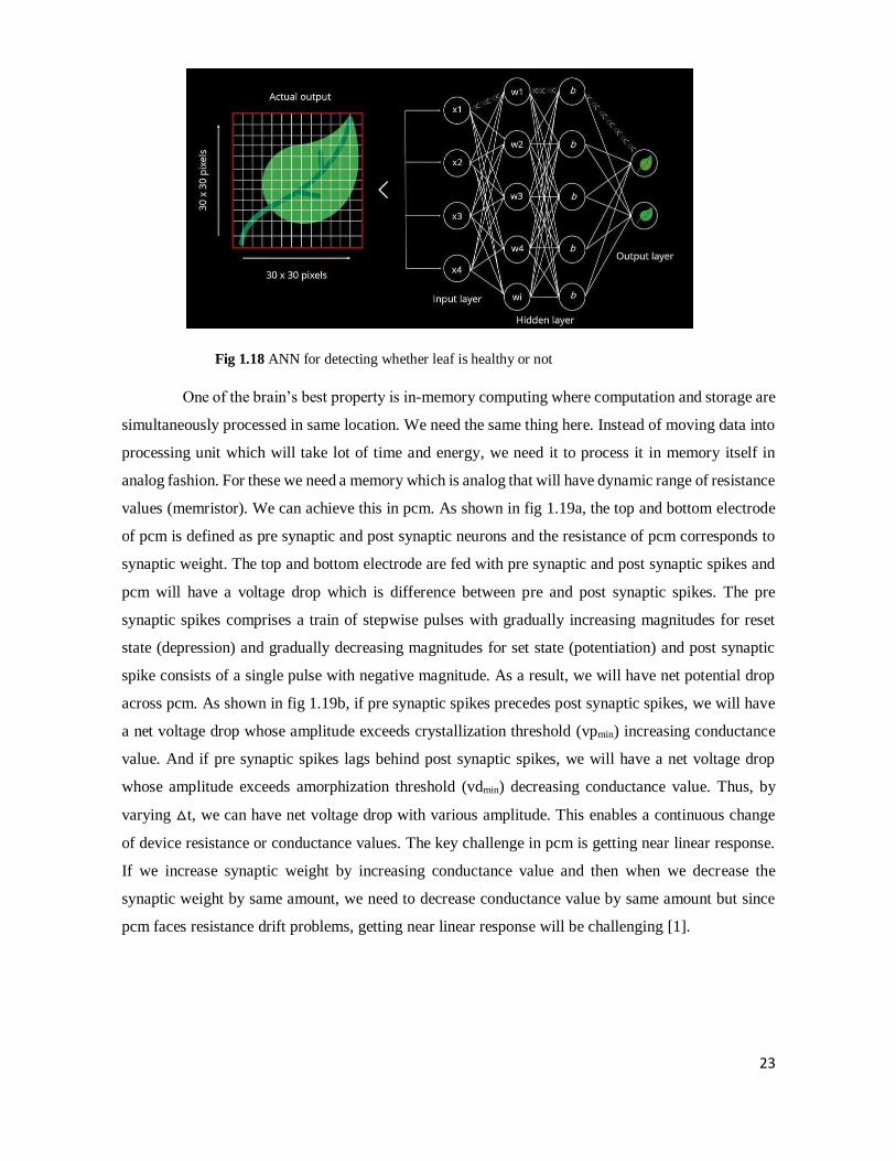
The STDP is used in Artificial neural network (ANN) to change synaptic weights. ANN are
used in application like speech and image recognition where we train the system with lot of input
values before using it for recognition. It uses perceptron model where all the inputs will be multiplied
with their synaptic weights and summed. This sum will be then compared with threshold value. If the
sum is above threshold, the neuron will fire else it will not fire. Conventional ANN usually consists of
input layer, hidden layer and output layer. Fig 1.18 is an example of ANN to recognise whether the
leaf is healthy or not. We will first do image segmentation and all this segmented image will be
multiplied with their synaptic weights and summed. If the total sum is greater than threshold then
neuron passes its signal to next layer. This procedure is repeated till it reaches output layer. At output
it will be decided whether the leaf is healthy or not. If suppose a leaf is healthy and shown as unhealthy,
we backtrack and change the synaptic weights such that it gives correct output. All this input and
synaptic weight multiplication process is done by matrix vector multiplication. In order to do this with
a digital design, we need to bring each and every one of these vector elements from memory into the
processing unit and do multiplication and addition and then these results are sent back to memory.
Doing all this will take lot of time and power consumption.
23
Fig 1.18 ANN for detecting whether leaf is healthy or not
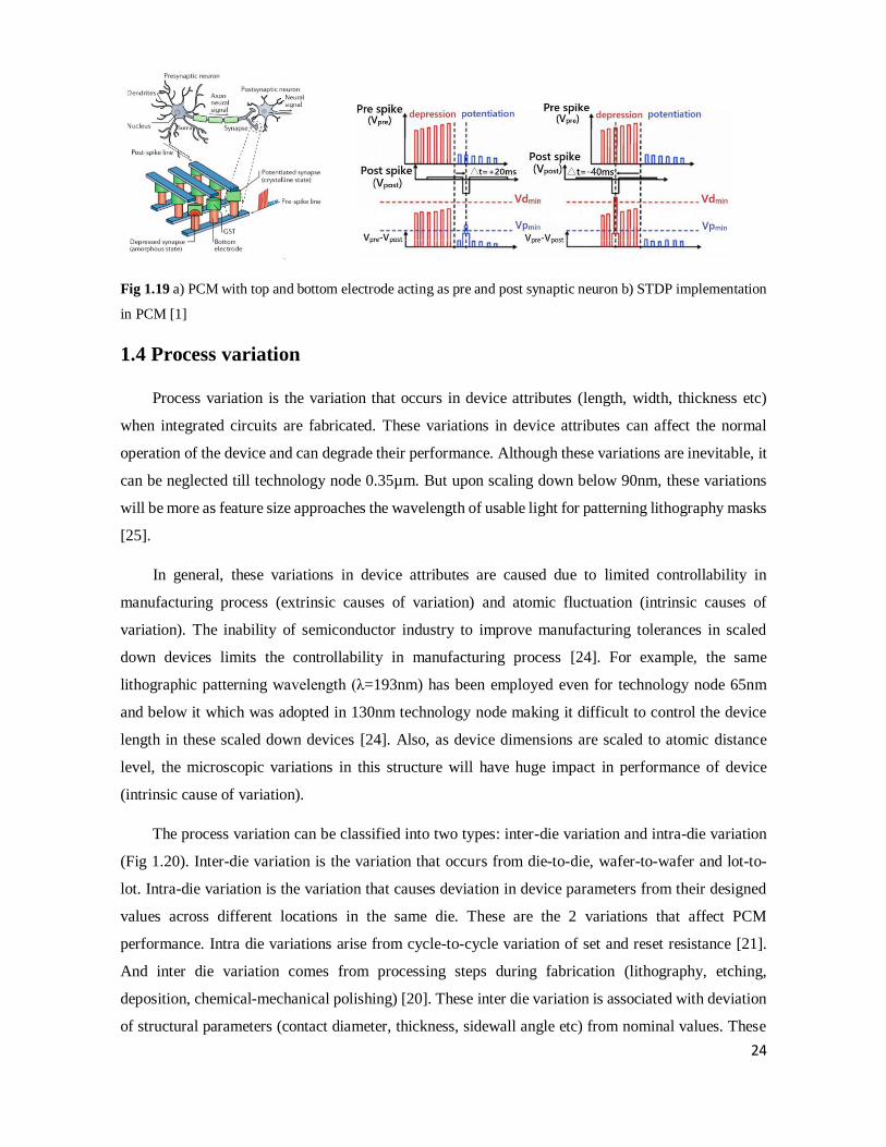
One of the brain’s best property is in-memory computing where computation and storage are
simultaneously processed in same location. We need the same thing here. Instead of moving data into
processing unit which will take lot of time and energy, we need it to process it in memory itself in
analog fashion. For these we need a memory which is analog that will have dynamic range of resistance
values (memristor). We can achieve this in pcm. As shown in fig 1.19a, the top and bottom electrode
of pcm is defined as pre synaptic and post synaptic neurons and the resistance of pcm corresponds to
synaptic weight. The top and bottom electrode are fed with pre synaptic and post synaptic spikes and
pcm will have a voltage drop which is difference between pre and post synaptic spikes. The pre
synaptic spikes comprises a train of stepwise pulses with gradually increasing magnitudes for reset
state (depression) and gradually decreasing magnitudes for set state (potentiation) and post synaptic
spike consists of a single pulse with negative magnitude. As a result, we will have net potential drop
across pcm. As shown in fig 1.19b, if pre synaptic spikes precedes post synaptic spikes, we will have
a net voltage drop whose amplitude exceeds crystallization threshold (vpmin) increasing conductance
value. And if pre synaptic spikes lags behind post synaptic spikes, we will have a net voltage drop
whose amplitude exceeds amorphization threshold (vdmin) decreasing conductance value. Thus, by
varying t, we can have net voltage drop with various amplitude. This enables a continuous change
of device resistance or conductance values. The key challenge in pcm is getting near linear response.
If we increase synaptic weight by increasing conductance value and then when we decrease the
synaptic weight by same amount, we need to decrease conductance value by same amount but since
pcm faces resistance drift problems, getting near linear response will be challenging [1].
24
Fig 1.19 a) PCM with top and bottom electrode acting as pre and post synaptic neuron b) STDP implementation
in PCM [1]
1.4 Process variation
Process variation is the variation that occurs in device attributes (length, width, thickness etc)
when integrated circuits are fabricated. These variations in device attributes can affect the normal
operation of the device and can degrade their performance. Although these variations are inevitable, it
can be neglected till technology node 0.35µm. But upon scaling down below 90nm, these variations
will be more as feature size approaches the wavelength of usable light for patterning lithography masks
[25].
In general, these variations in device attributes are caused due to limited controllability in
manufacturing process (extrinsic causes of variation) and atomic fluctuation (intrinsic causes of
variation). The inability of semiconductor industry to improve manufacturing tolerances in scaled
down devices limits the controllability in manufacturing process [24]. For example, the same
lithographic patterning wavelength (λ=193nm) has been employed even for technology node 65nm
and below it which was adopted in 130nm technology node making it difficult to control the device
length in these scaled down devices [24]. Also, as device dimensions are scaled to atomic distance
level, the microscopic variations in this structure will have huge impact in performance of device
(intrinsic cause of variation).
The process variation can be classified into two types: inter-die variation and intra-die variation
(Fig 1.20). Inter-die variation is the variation that occurs from die-to-die, wafer-to-wafer and lot-to-
lot. Intra-die variation is the variation that causes deviation in device parameters from their designed
values across different locations in the same die. These are the 2 variations that affect PCM
performance. Intra die variations arise from cycle-to-cycle variation of set and reset resistance [21].
And inter die variation comes from processing steps during fabrication (lithography, etching,
deposition, chemical-mechanical polishing) [20]. These inter die variation is associated with deviation
of structural parameters (contact diameter, thickness, sidewall angle etc) from nominal values. These

25
deviations in structural parameters primarily affects the temperature profile and since electrical
operations of PCM (set and reset operations) depends on joule heating, it will affect the device
electrical characteristics.
Fig 1.20 Illustration of inter-die and intra-die variations [26]
1.4.1 Geometrical Aspect Ratio (AR):
Generally, in nano-scale device architectures, due to process variation it is ideally difficult to
fabricate devices with circular cross-section. Due to limitations in manufacturing process instead of
circular cross-section, devices end up with elliptical cross-section with major and minor axis. This can
be defined by a geometrical parameter called Aspect ratio (AR). It is defined as a ratio of length of
major axis to that of minor axis. If AR is greater than 1, devices shows expanded ellipse structure and
if AR is less than 1, devices shows compressed ellipse structure. For ideal circular cross-section, AR
should be 1 [23]. This impact of geometrical AR has already been studied in devices like SONOS and
gate all around FINFET (GAA). It is very difficult to predict what AR, the device will have. So, in an
array of PCM cells, the device with largest AR decides the current driving capability of selector device
for reset operation. So, we need to choose a selector device with large area. But again, this high-power
programming is not good for cells having smaller AR as it will reduce endurance in these cells [22].
Fig 1.21 Illustration of different geometrical AR varying from 0.5 to 1.75 [23]

26
1.5 Objective of thesis:
In PCM device architecture like mushroom and pore-type cell, area of heater and pore plays an
important role, and thereby geometrical AR plays a major role in these devices with circular cross-
section. The mushroom type and pore type device architectures employing Ge2Sb2Te5 are most studied
and utilised in commercial products. So, in this study, we will be seeing how this geometrical AR
affects the performance of these device architecture (mushroom and pore-type) and which device is
more sensitive to these variations. The objectives of thesis are as follows:
1) Impact of geometrical AR on the performance of scalable mushroom-type phase change
memory device.
2) Impact of geometrical AR on the performance of scalable pore-type phase change memory
device.
27
CHAPTER 2
SIMULATION METHODOLOGY
In this chapter, we will discuss the significance of Technology computer-aided design
(TCAD) and the various modules available in the TCAD simulator. Also, the interconnection
between the analytical phase- transition model and the electro-thermal model has been discussed
for a systematic understanding of the programming characteristics of the PCM device.
2.1 Introduction
The ability of computational tools to accurately model the device behaviour and predict
device limitations is of utmost importance. In this aspect, device CAD has been extensively used to
predict the performance of conceptual semiconductor device designs in terms of numerical
simulations. Also, the device CAD is useful to calibrate models with experimental data and then use
the calibrated models in the optimization phase of the devices in the development process [27-29].
The numerical simulation of semiconductor device operation/fabrication is extremely useful,
where it provides insights into complex phenomena that cannot be probed through experiments [30].
The physical phenomena that occur in semiconductor device/processes can be modelled by partial
differential equations (PDEs), and therefore, the device CAD is based on the solution of PDEs [27].
The significant advantages of the predictive power of device CAD are to reduce the time and cost
involved in the research and development of the product.
Sentaurus Device (Synopsys, 2016.03) simulates numerically the electrical/optical/thermal
behavior of a single semiconductor device in isolation or the several physical devices connected
together in a circuit [31]. It can simulate geometries (1D, 2D, 3D and 2D cylindrical) over a wide
range of operating conditions, and also mixed-mode circuit simulation can be performed by combining
several devices with the help of compact models. In general, charges, currents and voltages generated
at device terminals are computed based on a set of physical device equations that describe the carrier
transport and distribution. It also comprises of advanced physical models and robust numeric solvers
for the simulation of various kinds of silicon and non-silicon based semiconductor devices such as
very deep submicron MOSFETs, solar cells, memories, large bipolar power structures, etc. [31].
2.2 Sentaurus TCAD
Sentaurus TCAD from Synopsys is used in this thesis [31]. There are various modules available
in Sentaurus TCAD and the following modules have been used in the PCM device simulation.

28
Sentaurus Structure Editor (SDE)
Sentaurus Device (SDEVICE)
Inspect
Sentaurus Visual (SVISUAL) These modules are discussed as follows
2.2.1 Sentaurus Structure Editor
The primary step of the TCAD tool flow is to create a structure for device simulation using
Sentaurus structure editor (SDE) tool. This SDE tool can be used to generate both 2D and 3D
structures described by appropriate contacts and materials. The doping distributions are defined with
the help of an analytical profile. Followed by, a suitable mesh for the device should be adopted for
the finite element method (FEM) simulation [32]. The dense/fine mesh is required, particularly in
the sensitive regions such as interfaces between different materials, higher electric field/current
density/charge generation regions and in the regions where interesting effects are estimated to occur.
The advantage of this tool is that novel device structures can be generated and tested
thoroughly before proceeding to the real fabrication process. This tool can be used to create several
basic geometrical shapes like rectangles, cuboids, spheres, cylinders, polygons and lines. Each of
these geometrical elements can be defined by the suitable material from the class of metals,
semiconductors or insulators (e.g. copper, aluminium, silicon, silicon dioxide, binary and ternary
alloys, user- defined materials, etc.). The input and output files which are supported by this SDE are
given as follows:
Input file: Scheme script file (.scm) is the user-defined editable script file that allows describing the
steps to create the 2D/3D device structure by using Scheme script commands.
Output file: The final device structure can be viewed and it is used as an input file for the SDEVICE
simulation.
2.2.2 Sentaurus Device (SDEVICE)
SDEVICE tool is used to solve the fundamental semiconductor equations for each mesh/grid
point in the 2D/3D device generated using SDE. An extensive set of models including drift-
diffusion, thermodynamic, hydrodynamic models, Fowler–Nordheim and direct tunnelling, hot-
carrier injection mechanisms for device physics are available to capture the physical effects in
semiconductor devices [31]. An efficient numerical method can be applied to solve 2D and 3D
device simulations with a trade-off between accuracy and computation time. Figure 2.1 shows the
flow diagram of SDEVICE. Furthermore, SDEVICE tool is very useful to model the device
electrical, thermal and optical characteristics without going to the real-time fabrication of the actual

29
device.
Fig 2.1 Sentaurus Device tool flow
It has the following characteristics [30]
• Extraction of the terminal currents and voltages of the simulated device and its I-V plot.
• The internal device operation can be understood better by visualizing the solution variables
including potential, electric field, lattice temperature, Joule heat, carrier distributions, current
density, generation and recombination rate.
Input File: The input file of SDEVICE tool consists of several command sections namely file,
electrode, physics, math, solve and plot sections. Each section serves to execute their independent
functions. The role of each section is described as follows:
File Section
It has one essential input file which consists of the information of device structure and an optional
material parameter file. It has many output files that contain the resulting charges, currents,
voltages, temperatures, etc., of all the terminals in a device.
Electrode Section
Indicates electrical and thermal contacts of the device, and also initial biasing and boundary
conditions of each contact can be defined.
Physics Section
The physics section declares the physical models to be activated in the simulation. Some of the
models are carrier mobility model, apparent band edge shift model, impact ionization model,
30
SRH recombination model, analytical phase transition model, and state-dependent
mobility/thermal conductivity/heat capacity models [31].
Physical models can be activated globally or it can be restricted to specific materials or regions
of interest in a device.
Math Section The device equations in terms of PDE are solved in an iterative manner in all the mesh points.
An error is calculated for each and every iteration step, and tries to converge to a solution with a
minimum acceptable error. In addition, the number of iterations, type of numeric solver, relative
error control can be mentioned.
Solve Section
The build-up of the initial solution is obtained using the Poisson equation in order to reach the
equilibrium condition in the device. Poisson equation and carrier continuity equation are solved
self-consistently using Newton solver.
Plot Section
The solution variables like carrier concentration, current densities, lattice temperature, carrier
Joule heat, electric potential, etc., can be visualized using SVISUAL by declaring the variables
under the Plot command.
Physical Models
The selection of physical models is a primary task to get realistic results in the device
simulator. The carrier transport models available are drift-diffusion model (DD), thermodynamic
model (Thermo), and hydrodynamic model (HD) [31]. The DD solves self-consistently the Poisson
and the carrier continuity equations. The Thermo accounts electro-thermal effects by extending the
drift-diffusion approach under the assumption that the charge carriers maintain thermal equilibrium
with the lattice. The Thermo solves the lattice heat equation in addition to the Poisson and the carrier
continuity equations [31]. On the other hand, the HD is used to solve the carrier (electron/hole)
temperature and lattice heat equation in addition to the Poisson and the carrier continuity equations
[31].
The other physical models used in PCM device simulation are apparent band edge shift
model, carrier mobility model, Shockley-Read- Hall (SRH) recombination model, SRH surface
recombination model, impact ionization model, state-dependent mobility/thermal conductivity/heat
capacity model. In this study, simulations are carried out using the DD transport mechanism and the
lattice heat equation.
2.2.3 Sentaurus Visual (SVISUAL)

31
SVISUAL is used to view results created by simulation tools in 1D/2D/3D. It also assists in
understanding the physical processes captured during fast transient simulations. This plotting tool
can probe data fields in any coordinates of interest in the device, to make cut-lines and cut-planes,
and to perform analysis on data fields from simulation results.
2.2.4 Inspect
This is a plotting and analysis tool for 2D data (XY plots) like doping concentration and
electrical/thermal characteristics of the devices. It has a sophisticated graphical user interface
(GUI), a script language for manipulating curves, and also features a large set of mathematical
functions such as differentiation, integration, etc.
2.3 Interconnection of Models for PCM Device Calibration
In this section, the models for the amorphous and crystalline phase of GST phase-change
material are discussed briefly and the interconnection of models is described in order to realize the
SET and RESET operations and the programming characteristics of the PCM device.
The ordered crystalline and the disordered amorphous GST phase- change material has a
bandgap of 0.5 eV and 0.7 eV [35], respectively. The crystalline GST is treated as a p-type
semiconductor due to the existence of vacancies [34]. The amorphous GST models the acceptor
(1e18 cm-3) and donor traps (1e17 cm-3) at the appropriate energy levels in the energy gap of 0.7 eV
[34]. Since the carrier transport differs with respect to phase, the apparent band edge shift (ABES)
models a variation in the carrier densities upon phase transition [31]. The valence band edge shift
of 0.2 eV produces a change in the trap energies and thereby modulates the hole and trap densities.
The carrier mobility, trap energies and trap densities are the important parameters to control the
resistance of the crystalline and amorphous GST.
Further, the surface SRH recombination model is used to capture the excess carrier dissipation
at disordered GST/metal interface. In addition, multi-state mobility and thermal conductivity models
are employed to capture the variation of mobility and thermal conductivity values in two different
phases [31]. The temperature-dependent thermal conductivity of GST material has also been
accounted individually for crystalline and amorphous states. Besides, the electronic nature of
threshold switching phenomena during the SET process is described by the interplay between
recombination and impact ionization process [35]. This phenomenon is captured by employing the
Okuto-Crowel impact ionization model [36] and the SRH recombination model [37].
The electrical quantities are computed by the drift-diffusion equation, whereas the lattice heat
equation is used to calculate the lattice temperature spatially and temporally across the device [34].
32
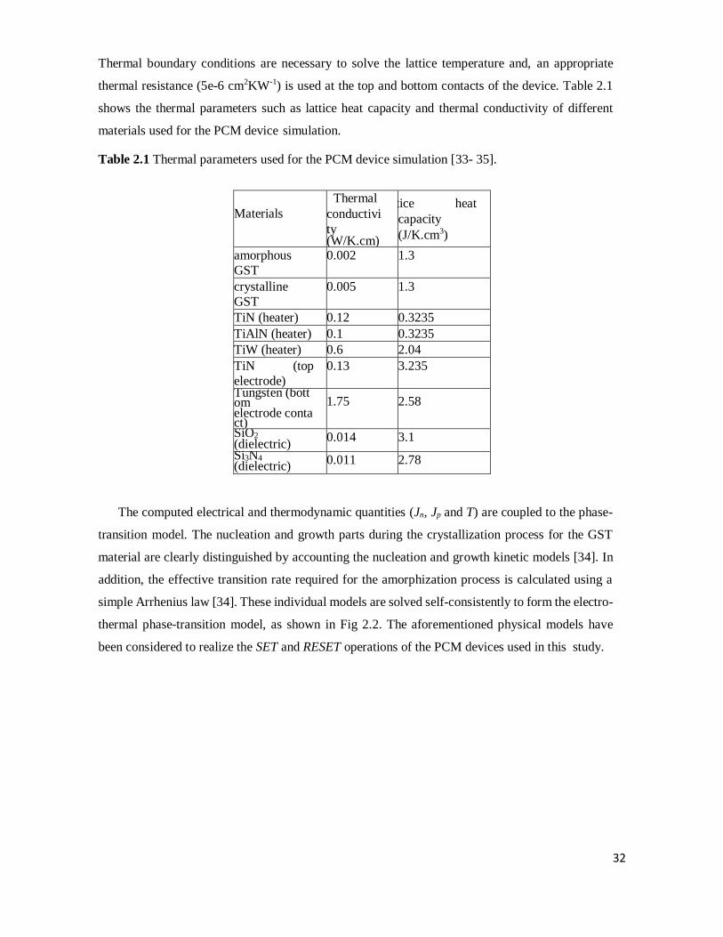
Thermal boundary conditions are necessary to solve the lattice temperature and, an appropriate
thermal resistance (5e-6 cm2KW-1) is used at the top and bottom contacts of the device. Table 2.1
shows the thermal parameters such as lattice heat capacity and thermal conductivity of different
materials used for the PCM device simulation.
Table 2.1 Thermal parameters used for the PCM device simulation [33- 35].
Materials
Thermal
conductivi
ty (W/K.cm)
Lattice heat
capacity
(J/K.cm3)
amorphous
GST
0.002 1.3
crystalline
GST
0.005 1.3
TiN (heater) 0.12 0.3235
TiAlN (heater) 0.1 0.3235
TiW (heater) 0.6 2.04
TiN (top
electrode)
0.13 3.235
Tungsten (bottom electrode contact)
1.75 2.58
SiO2 (dielectric)
0.014 3.1
Si3N4 (dielectric)
0.011 2.78
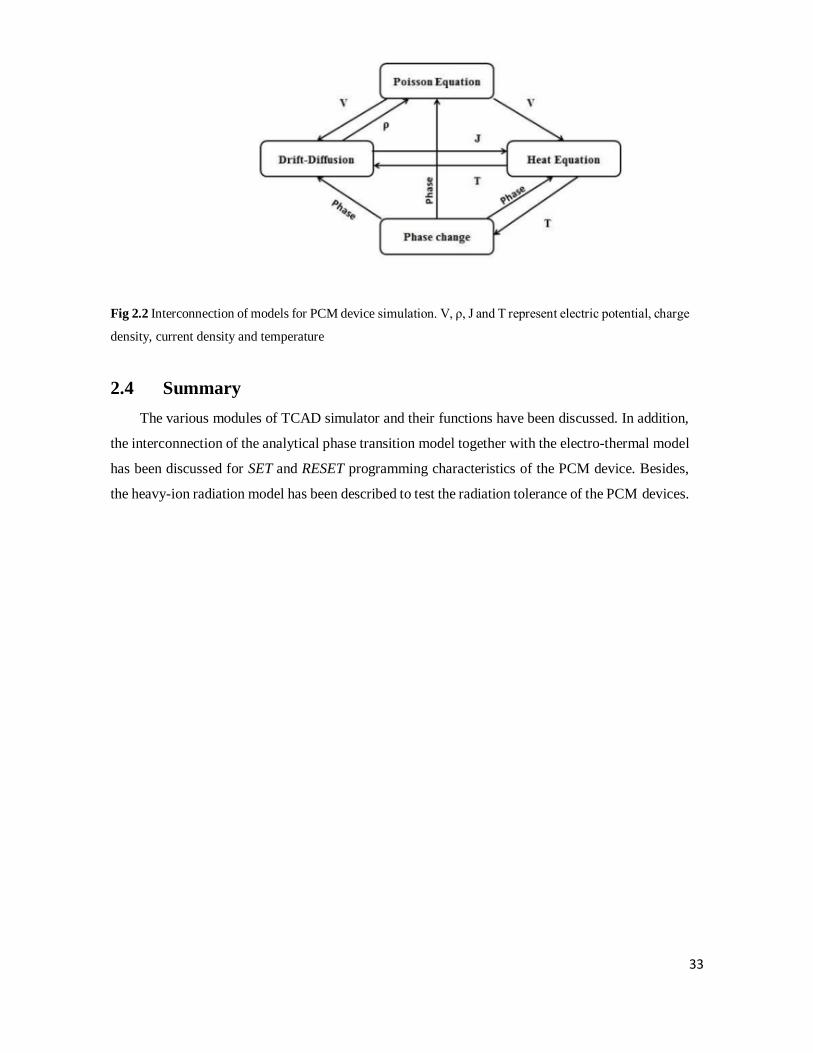
The computed electrical and thermodynamic quantities (Jn, Jp and T) are coupled to the phase-
transition model. The nucleation and growth parts during the crystallization process for the GST
material are clearly distinguished by accounting the nucleation and growth kinetic models [34]. In
addition, the effective transition rate required for the amorphization process is calculated using a
simple Arrhenius law [34]. These individual models are solved self-consistently to form the electro-
thermal phase-transition model, as shown in Fig 2.2. The aforementioned physical models have
been considered to realize the SET and RESET operations of the PCM devices used in this study.
33
Fig 2.2 Interconnection of models for PCM device simulation. V, ρ, J and T represent electric potential, charge
density, current density and temperature
2.4 Summary
The various modules of TCAD simulator and their functions have been discussed. In addition,
the interconnection of the analytical phase transition model together with the electro-thermal model
has been discussed for SET and RESET programming characteristics of the PCM device. Besides,
the heavy-ion radiation model has been described to test the radiation tolerance of the PCM devices.

34
CHAPTER 3
IMPACT OF GEOMETRICAL ASPECT RATIO ON THE
PERFORMANCE OF MUSHROOM-TYPE PCM DEVICE
In this chapter, the impact of geometrical AR on electrical characteristics of mushroom-type phase
change memory device have been studied. All the simulations are done in Sentaurus TCAD. The
device electrical characteristics like reset current, reset resistance and their temperature profile are
investigated for heater diameter of 100nm and 20nm with different AR values. Totally, three cases
are taken in this study. In case 1, the change in heater AR alone has been considered. In case 2, the
change in GST AR alone has been considered and in case 3, both the changes in heater and GST
AR have been considered. It is observed that reset current reduces for smaller AR of heater and
increases for higher AR of heater. The change in GST AR didn’t affect reset current much for heater
diameter of 100nm whereas it got reduced for smaller AR (0.5) in 20nm device.
3.1 Introduction
To outpace the increasing rate of global data (digitalization), to fill the gap in memory hierarchy
(to overcome memory wall problem) and for future computing applications like neuromorphic,
many new memory technologies have been explored. Among them, PCM seems to be a promising
one with its attractive features like high endurance, long data retention, high speed and high density.
PCM also exhibit high scalability. The active material can be scaled down even below 2nm
dimensions [39,40]. However as the device dimension approaches nanoscale regime, it becomes
difficult to control the manufacturing process. This is due to the inability of semiconductor industry
to improve manufacturing tolerances in scaled down devices which limits the controllability in
manufacturing process [24]. As a result, there will be variations in device attributes (contact
diameter, thickness etc) from their nominal value which are commonly referred as process variation.
These variations in device attributes can lead to variations in electrical characteristics which will
affect the normal operation (set and reset) of PCM device.
In nano-scale device architecture, it is difficult to fabricate a perfect circular cross-section [41].
Due to process variation, devices come with an elliptical cross-section instead of circular cross-
section. This can be defined by a parameter called aspect ratio (AR). It is defined as the ratio of
length of major axis to that of minor axis. An aspect ratio of 1 gives circular cross section. Other
than value of 1 gives elliptical cross-section. Generally, all the values are calculated for nominal
case assuming perfect circular cross-section. But since it’s difficult to have a circular cross-section,
35
we are ended up with elliptical cross section with different aspect ratio. Different aspect ratios will
have different area. In specific devices like mushroom-type phase change memory device, where
the circular cross-section of heater plays an important role in Joule heating for reset operation, these
variation in area from nominal case can lead to variation in electrical characteristics.
Also, due to its statistical nature, it is quite challenging to predict aspect ratio of a device [41].
So, in a memory array, if we get cells with different AR values then different cells can respond
differently for a given set, reset and read pulse. These variations can exacerbate for multi-level cells
where the resistance contrast between intermediate level would be small enough to degrade the
reliability of individual cells [42]. Therefore, it is important to investigate the impact of geometrical
AR on performance of mushroom-type phase change memory device in order to predict the
allowable tolerances in such non circular cross-section device.
This chapter is organised as follows: section 3.2 describes device structure, their dimensions
and materials used. Section 3.3 describes about the method of simulation and finally section 3.4
discusses the results of this experiment.
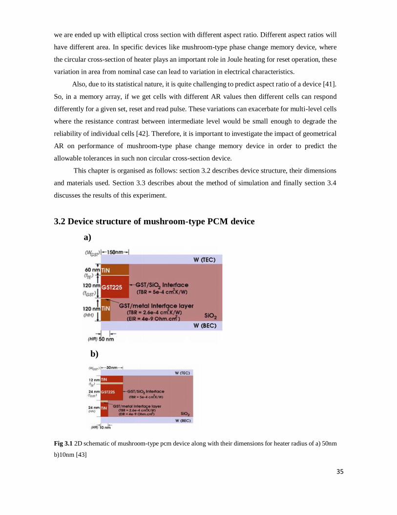
3.2 Device structure of mushroom-type PCM device
a)
b)
Fig 3.1 2D schematic of mushroom-type pcm device along with their dimensions for heater radius of a) 50nm
b)10nm [43]

36
Fig 3.1 shows the 2D schematic of mushroom-type PCM device with their dimensions. Here
BEC and TEC refers to top and bottom electrode contacts. The material used as TEC and BEC is
tungsten. And TE, BE refers to top and bottom electrode also can be called as heater and sinker. The
material used as TE and BE is TiN. The structure consists of GST active material sandwiched
between heater (TiN) and sinker (TiN) and surrounded by oxide for thermal insulation. The whole
structure is then connected to TEC and BEC.
And Fig 3.2 shows a TCAD generated 3D cylindrical mushroom-type device structure with
circular cross-section after removing oxide, TEC and BEC. All the dimensions of TE, BE, GST are
same as shown in fig 3.1. These devices considered interfacial effects between GST/TE, GST/BE
and GST/SiO2. The TBR and EIR values of bottom and top interface are taken as 2.6e-4 cm2.K/W,
4e-9 Ω/cm2 and the interface thickness is 3nm. The TBR value for GST/SiO2 is taken as 5e-4
cm2.K/W and since EIR value for GST/SiO2 is so large, it is assumed to have no effect and ignored
in simulation.
TiN GST225 interface
Fig 3.2 TCAD generated 3D cylindrical mushroom type pcm with circular cross-section after removing
oxide and tungsten.
3.3 Simulation method
To study the impact of geometrical AR on reset operation of mushroom type device structure,
the reset current and reset resistance values have been calculated for nominal case of AR=1 i.e., for
perfect circular cross-section. Initially the active GST material is in crystalline state. Here to
accomplish reset operation, current pulse with pulse parameter 1ns/40ns/1ns is applied and
corresponding reset current value is identified from R-I characteristics where saturation of resistance
takes place. For heater diameter of 100nm, the reset current value is shown as 1.5mA with reset
resistance of 811kΩ. In case of scaled down device with heater diameter of 20nm, the reset current

37
is observed as 220µA with reset resistance of 19MΩ (fig 3.3). These values are considered as
nominal values. The heater cross-section is changed by changing AR. For this, the minor axis length
is fixed and the major axis length is varied, hereby achieving different AR values. The
corresponding reset current and resistance values for different AR values are observed and
compared with the nominal values. The device structure is calibrated with [43] and the reset current
values obtained for 100nm and 20nm in nominal case is in accordance with the values reported in
literature [43].
Totally, in the present study, three cases are considered. Case 1 corresponds to changing the
AR of heater alone. Case 2 corresponds to change in the AR of GST alone and in case 3, the AR of
both heater and GST is changed.
a) b)
Fig 3.3 R-I characteristics for nominal case (AR=1) for heater diameter of a) 100nm b)20nm
3.4 Results and discussion
Case 1: change in AR of heater alone
AR=0.5 0.75 1 1.25 1.5 1.75
heater GST
Fig 3.4a indicates as the AR is decreased from 1 to 0.75 to 0.5 for heater diameter of 100nm, the
Ireset value is decreased from 1.5mA to 1.3mA to 1.1mA. And as the AR is increased from 1 to 1.25
to 1.5, the Ireset value increased from 1.5mA to 1.8mA to 2mA and for AR of 1.75, the Ireset value is
2.2mA. Thus, the reset current is shown to be decreasing from nominal value for smaller AR and
increasing from nominal value for higher AR values. Also, the graph exhibits almost linear nature.

38
The behaviour in reset current can be explained by temperature profile shown in fig 3.4c. we know
that area of heater plays an important role in Joule heating for reset operation. For smaller AR,
heater area decreases and Joule heating increases thus giving rise to high temperature for a given
current value compared to nominal case. So, saturation in reset resistance occurs before nominal
value and the saturated reset resistance value is higher than nominal value (fig 3.4b). And for higher
AR, heater area increases and Joule heating decreases thus giving low temperature for a given
current value compared to nominal case. So, saturation in reset resistance occurs after nominal value
and the saturated reset resistance value is higher than nominal value. Also, the current density (reset
current/ heater area) values are shown to be increasing as AR is decreasing and vice versa (fig 3.4d).
But the decrease in current density is less for higher AR than compared to increase in current density
for smaller AR. The same behaviour is seen for scaled down device for heater diameter 20nm (fig
3.5) also. But when compared to 100nm, the percentage change in reset current value is less in 20nm
as shown in fig 3.6

39
a) b)
c) d)
Fig 3.4 a) Reset current values for AR varying from 0.5 to 1.75 for heater diameter of 100nm b) Reset
resistance values for AR varying from 0.5 to 1.75 for heater diameter of 100nm c) Maximum lattice
temperature obtained for AR varying from 0.5 to 1.75 for heater diameter of 100nm for nominal reset current
value of 1.5mA d) Current density values for AR varying from 0.5 to 1.75 for heater diameter of 100nm

40
a) b)
c) d)
Fig 3.5 a) Reset current values for AR of heater varying from 0.5 to 1.75 for scaled down device for heater
diameter 20nm b)Reset resistance values for AR of heater varying from 0.5 to 1.75 for 20nm c) Maximum
lattice temperature obtained for AR of heater varying from 0.5 to 1.75 for 20nm for nominal reset current
value of 220µA d) Current density values for AR of heater varying from 0.5 to 1.75 for 20nm
41
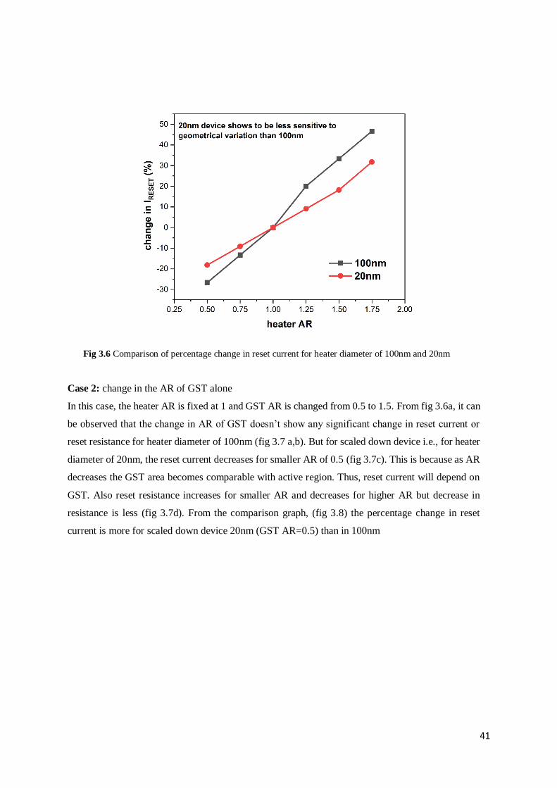
Fig 3.6 Comparison of percentage change in reset current for heater diameter of 100nm and 20nm
Case 2: change in the AR of GST alone
In this case, the heater AR is fixed at 1 and GST AR is changed from 0.5 to 1.5. From fig 3.6a, it can
be observed that the change in AR of GST doesn’t show any significant change in reset current or
reset resistance for heater diameter of 100nm (fig 3.7 a,b). But for scaled down device i.e., for heater
diameter of 20nm, the reset current decreases for smaller AR of 0.5 (fig 3.7c). This is because as AR
decreases the GST area becomes comparable with active region. Thus, reset current will depend on
GST. Also reset resistance increases for smaller AR and decreases for higher AR but decrease in
resistance is less (fig 3.7d). From the comparison graph, (fig 3.8) the percentage change in reset
current is more for scaled down device 20nm (GST AR=0.5) than in 100nm

42
a) b)
c) d)
Fig 3.7 a) Reset current values for AR of GST varying from 0.5 to 1.75 for heater diameter 100nm b) Reset
resistance values for AR of GST varying from 0.5 to 1.75 for 100nm c) Reset current values for AR of GST
varying from 0.5 to 1.75 for scaled down device for heater diameter 20nm d) Reset resistance values for AR of
GST varying from 0.5 to 1.75 for 20nm
Fig 3.8 Comparison of percentage change in reset current for heater diameter of 100nm and 20nm.

43
Case 3: change in the AR of both GST and heater
In this case, the reset current value is almost same as that of the values observed in case 1 for 100nm.
But for scaled down 20nm, the reset current is decreased to 31% for the case with GST and heater
AR of 0.5.
Table 3.1 Reset current and resistance values for heater diameter of 100nm. Here r: AR of heater
r1: AR of GST hd: heater diameter
r1 r hd (nm) IRESET (mA) RRESET (MΩ) %I %R
0.5 0.5 100 1.1 1.34 -26.67 +65.4
1.5 0.5 100 1.1 1.34 -26.67 +65.4
1.5 1.5 100 2 0.53 +33.33 -33.5
Table 3.2 Reset current and resistance values for heater diameter of 20nm
r1 r hd (nm) IRESET (µA) RRESET (MΩ) %I %R
0.5 0.5 20 150 42 -31.81 +121
0.5 1.5 20 200 28 -9.09 +47.3
1.5 0.5 20 180 27 -18.18 +42.1
1.5 1.5 20 270 13 +22.72 -31.5
44
CHAPTER 4
IMPACT OF GEOMETRICAL ASPECT RATIO ON THE
PERFORMANCE OF PORE-TYPE PCM DEVICE
In this chapter, the impact of geometrical AR on the electrical characteristics of pore-type PCM
device have been studied. All the simulations are done using Sentaurus TCAD. The device electrical
characteristics like reset current, reset resistance and their temperature profile have been studied for
device with pore diameter of 100nm and for scaled down device with pore diameter of 20nm. By
varying the AR of pore diameter from 0.5 to 1.75, the variation in reset current is observed. It is
shown that reset current increases for decreasing AR and decreases for increasing AR. Finally, the
comparison between mushroom and pore-type has been done to see which device architecture shows
more impact to geometrical variation of cross-section and conclusion is drawn.
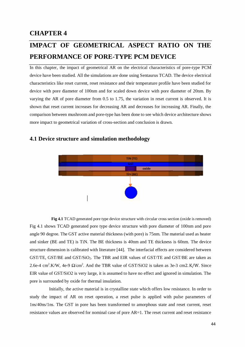
4.1 Device structure and simulation methodology
Fig 4.1 TCAD generated pore type device structure with circular cross section (oxide is removed)
Fig 4.1 shows TCAD generated pore type device structure with pore diameter of 100nm and pore
angle 90 degree. The GST active material thickness (with pore) is 75nm. The material used as heater
and sinker (BE and TE) is TiN. The BE thickness is 40nm and TE thickness is 60nm. The device
structure dimension is calibrated with literature [44]. The interfacial effects are considered between
GST/TE, GST/BE and GST/SiO2. The TBR and EIR values of GST/TE and GST/BE are taken as
2.6e-4 cm2.K/W, 4e-9 Ω/cm2. And the TBR value of GST/SiO2 is taken as 3e-3 cm2. K/W. Since
EIR value of GST/SiO2 is very large, it is assumed to have no effect and ignored in simulation. The
pore is surrounded by oxide for thermal insulation.
Initially, the active material is in crystalline state which offers low resistance. In order to
study the impact of AR on reset operation, a reset pulse is applied with pulse parameters of
1ns/40ns/1ns. The GST in pore has been transformed to amorphous state and reset current, reset
resistance values are observed for nominal case of pore AR=1. The reset current and reset resistance
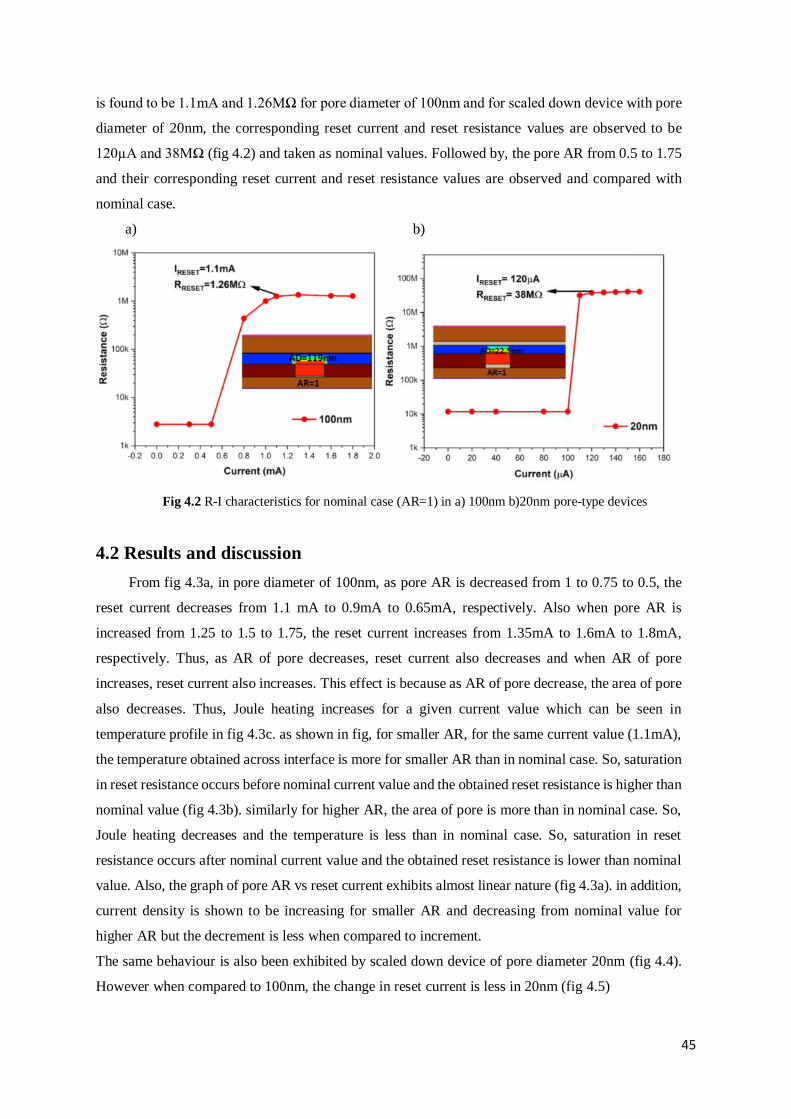
45
is found to be 1.1mA and 1.26MΩ for pore diameter of 100nm and for scaled down device with pore
diameter of 20nm, the corresponding reset current and reset resistance values are observed to be
120µA and 38MΩ (fig 4.2) and taken as nominal values. Followed by, the pore AR from 0.5 to 1.75
and their corresponding reset current and reset resistance values are observed and compared with
nominal case.
a) b)
Fig 4.2 R-I characteristics for nominal case (AR=1) in a) 100nm b)20nm pore-type devices
4.2 Results and discussion
From fig 4.3a, in pore diameter of 100nm, as pore AR is decreased from 1 to 0.75 to 0.5, the
reset current decreases from 1.1 mA to 0.9mA to 0.65mA, respectively. Also when pore AR is
increased from 1.25 to 1.5 to 1.75, the reset current increases from 1.35mA to 1.6mA to 1.8mA,
respectively. Thus, as AR of pore decreases, reset current also decreases and when AR of pore
increases, reset current also increases. This effect is because as AR of pore decrease, the area of pore
also decreases. Thus, Joule heating increases for a given current value which can be seen in
temperature profile in fig 4.3c. as shown in fig, for smaller AR, for the same current value (1.1mA),
the temperature obtained across interface is more for smaller AR than in nominal case. So, saturation
in reset resistance occurs before nominal current value and the obtained reset resistance is higher than
nominal value (fig 4.3b). similarly for higher AR, the area of pore is more than in nominal case. So,
Joule heating decreases and the temperature is less than in nominal case. So, saturation in reset
resistance occurs after nominal current value and the obtained reset resistance is lower than nominal
value. Also, the graph of pore AR vs reset current exhibits almost linear nature (fig 4.3a). in addition,
current density is shown to be increasing for smaller AR and decreasing from nominal value for
higher AR but the decrement is less when compared to increment.
The same behaviour is also been exhibited by scaled down device of pore diameter 20nm (fig 4.4).
However when compared to 100nm, the change in reset current is less in 20nm (fig 4.5)

46
a) b)
c) d)
Fig 4.3 a) Reset current values for AR varying from 0.5 to 1.75 for pore diameter of 100nm b)Rreset resistance
values for AR varying from 0.5 to 1.75 for pore diameter of 100nm c) Maximum lattice temperature obtained
for AR varying from 0.5 to 1.75 for 100nm pore diameter of 100nm for nominal reset current value of 1.1mA
d) Current density values for AR varying from 0.5 to 1.75 for pore diameter of 100nm

47
a) b)
c) d)
Fig 4.4 a) Reset current values for AR varying from 0.5 to 1.75 for pore diameter of 20nm b) Reset resistance
values for AR varying from 0.5 to 1.75 for pore diameter of 20nm c) Maximum lattice temperature obtained
for AR varying from 0.5 to 1.75 for 20nm pore diameter of 100nm for nominal reset current value of 120µA
d) Current density values for AR varying from 0.5 to 1.75 for pore diameter of 20nm

48
Fig 4.5 Comparison of percentage change in reset current for pore diameter of 100nm and 20nm.
4.3 Comparison of impact of AR on reset operation between mushroom-
type and pore-type
Among the two-device structure mushroom-type and pore-type, the pore type exhibits advantages
of low reset current and better endurance and mushroom-type has an advantage of low heat loss and
ease in deposition of phase change material. Now from the study of impact of geometrical variations
of cross-section, it is shown from fig 5.3, that pore-structure is more sensitive to geometrical
variations of cross-section than mushroom-type device structure. In this regard, mushroom type has
an advantage because in an array of PCM device, each cell can be with any AR and now with the
application of reset pulse of nominal value, the cells with higher AR may not be amorphized and
although the cells with smaller AR have smaller reset current value. This nominal value may consume
too much power and could result in reducing their endurance.
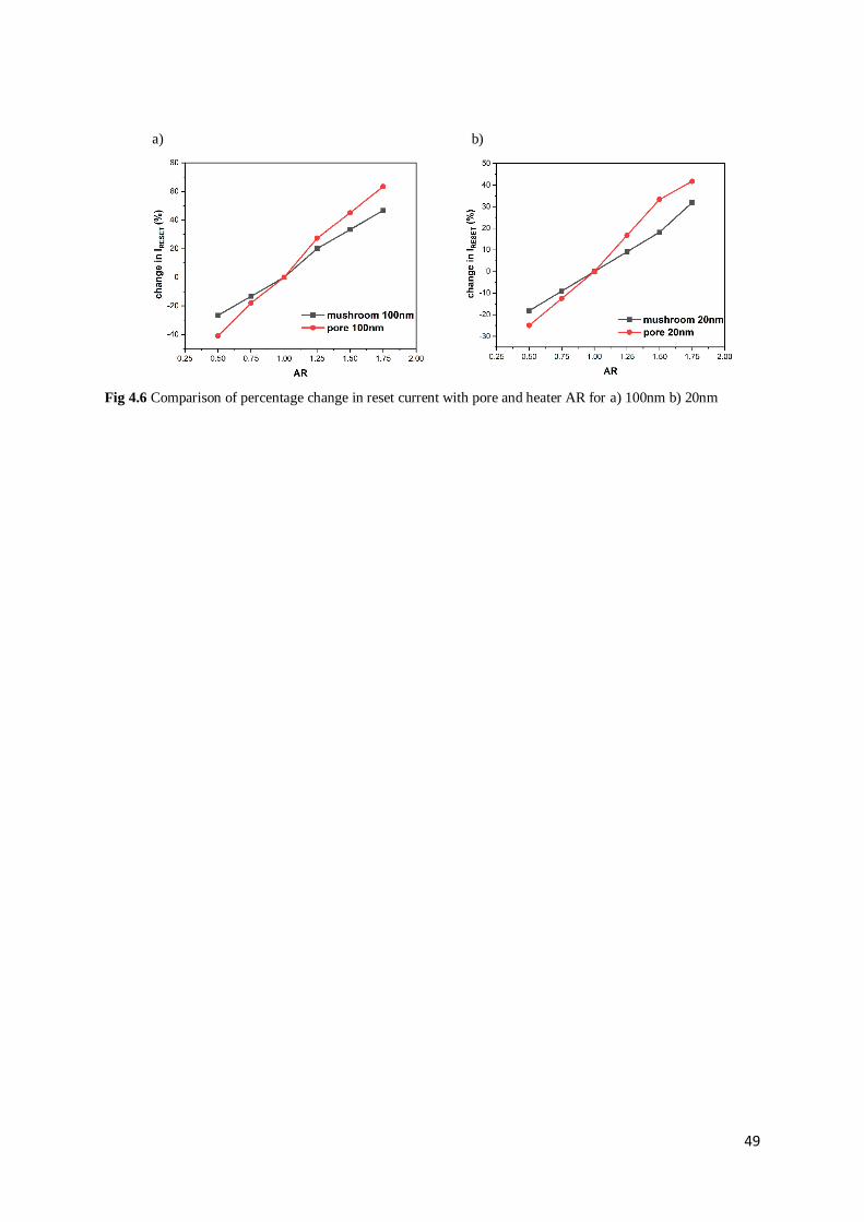
49
a) b)
Fig 4.6 Comparison of percentage change in reset current with pore and heater AR for a) 100nm b) 20nm
50
CHAPTER 5
CONCLUSION
In the present study, the conclusions of results are listed in the following:
In mushroom-type device, as AR of heater decreases, reset current decreases and as AR
increases, reset current increases.
The AR of GST didn’t affect reset current much in heater diameter of 100nm but for scaled
down device with heater diameter of 20nm the reset current got reduced for smaller AR (0.5).
For change in AR of both heater and GST, reset current is same as case1 in 100nm. For 20nm
also, it is almost same for higher AR of GST and reduced for GST and heater AR of 0.5
which is reduced by 31.81%
In pore-type device, as AR of pore decreases, reset current decreases and as AR increases,
reset current increases.
When compared to mushroom-type device, pore-type device shows to be more sensitive to
geometrical variations of cross-section.
In order to reset all cells in PCM array, a selector should be chosen with large area however
this again may reduce endurance for devices with smaller AR.
51
References:
[1] ZHI-CHENG LIU AND LEI WANG “Applications of Phase Change Materials in Electrical Regime From Conventional
Storage Memory to Novel Neuromorphic Computing” Digital Object Identifier 10.1109/ACCESS.2020.2990536
[2] D. Reinsel, J. Gantz, and J. Rydning, “Data Age 2025: The Digitization of the World From Edge to Core,” Int. Data Corp.,
28 (2018).
[3] Shimeng Yu, “Neuro-Inspired Computing With Emerging Nonvolatile Memory”, Proceedings of the IEEE, 2018
[4] T. Endoh, H. Koike, S. Ikeda, T. Hanyu, and H. Ohno, “An Overview of Nonvolatile Emerging Memories - Spintronics
for Working Memories,” IEEE Journal on Emerging and Selected Topics in Circuits and Systems, vol. 6, pp. 109–119, Jun
2016.
[5] G. Atwood, S. Deboer, K. Prall, and L. Somerville, “A semiconductor memory development and manufacturing
perspective,” Eur. Solid-State Device Res. Conf., pp. 1–6 (2014). doi: 10.1109/ESSDERC.2014.6948745
[6] Shimeng Yu and Pai-Yu Chen, “Emerging Memory Technologies”, IEEE SOLID-STATE CIRCUITS MAGAZINE
SPRING 2016
[7] R. Carboni and D. Ielmini, “Stochastic Memory Devices for Security and Computing,” Adv. Electron. Mater., 5, 9, 1–27.
(2019). doi: 10.1002/aelm.201900198
[8] Wei Zhang, Riccardo Mazzarello, Matthias Wuttig and Evan Ma, “Designing crystallization in phase-change materials for
universal memory and neuro-inspired computing”, Nature Reviews | Materials
[9] A. Sebastian, M. Le Gallo, and E. Eleftheriou, “Computational phase-change memory: Beyond von Neumann computing,”
J. Phys. D. Appl. Phys., 52, 44 (2019). doi: 10.1088/1361- 6463/ab37b6
[10] Andrea Redaelli, “Phase Change Memory Device Physics, Reliability and Application”, Springer International Publishing
AG 2018
[11] S. Raoux et al., “Phase-change random access memory: A scalable technology,” IBM J. Res. Dev., 52, 4–5, pp. 465–479
(2008). doi: 10.1147/rd.524.0465
[12] E. Bozorg-Grayeli, J. P. Reifenberg, M. Asheghi, H.-S. P. Wong, and K. E. Goodson, “Thermal Transport in Phase
Change Memory Materials,” Annu. Rev. Heat Transf., 16, 1, 397–428 (2013). doi: 10.1615/annualrevheattransfer.v16.130
[13] D. Campi, D. Donadio, G. C. Sosso, J. Behler, and M. Bernasconi, “Electron-phonon interaction and thermal boundary
resistance at the crystal-amorphous interface of the phase change compound GeTe,” J. Appl. Phys., 117, 1 (2015). doi:
10.1063/1.4904910
[14] J. Lee, E. Bozorg-Grayeli, S. Kim, M. Asheghi, H. S. Philip Wong, and K. E. Goodson, “Phonon and electron transport
through Ge2Sb2Te5 films and interfaces bounded by metals,” Appl. Phys. Lett., 102, 19 (2013). doi: 10.1063/1.4807141
[15] D. Roy, “Characterization of electrical contacts for phase change memory cells,” Ph.D. Thesis, University of Twente,
Enschede, Netherlands (2011).
[16] Matthias Wuttig and Noboru Yamada, “Phase-change materials for rewriteable data storage”, nature materials, VOL 6,
NOVEMBER 2007
[17] Mohammed A. Zidan, John Paul Strachan and Wei D. Lu , “The future of electronics based on memristive systems”,
Nature Electronics | VOL 1 | JANUARY 2018
[18] Abu Sebastian, Manuel Le Gallo, Geoffrey W. Burr, Sangbum Kim, Matthew BrightSky, and Evangelos Eleftheriou,
“Tutorial: Brain-inspired computing using phase-change memory devices”, JOURNAL OF APPLIED PHYSICS 124, 111101
(2018)
[19] Javier del Valle, Juan Gabriel Ramírez, Marcelo J. Rozenberg, and Ivan K. Schuller, “Challenges in materials and devices

52
for resistive-switching-based neuromorphic computing”, JOURNAL OF APPLIED PHYSICS 124, 211101 (2018)
[20] G. W. Burr et al., “Phase change memory technology,” J. Vac. Sci. Technol. B, Nanotechnol. Microelectron. Mater.
Process. Meas. Phenom., 28, 2, 223–262 (2010). doi: 10.1116/1.3301579
[21] M. Boniardi, A. Redaelli, A. Ghetti, and A. L. Lacaita, “Study of cycling-induced parameter variations in phase change
memory cells,” IEEE Electron Device Lett., 34, 7, 882–884 (2013). doi: 10.1109/LED.2013.2261859
[22] M. H. Lee et al., “The impact of hole-induced electromigration on the cycling endurance of phase change memory,” in
International Electron Devices Meeting, pp. 28.6.1-28.6.4 (2010). doi: 10.1109/IEDM.2010.5703440
[23] Yiming Li1, and Chih-Hong Hwang, “The effect of the geometry aspect ratio on the silicon ellipse-shaped
surroundinggate field-effect transistor and cir”, 2009 Semicond. Sci. Technol. 24 095018
[24] M. Orshansky, S. R. Nassif, and D. Boning, "Design for manufacturability and statistical design:A constructive approach,"
US Springer, 2008.
[25] Geoffrey W. Burr et al., “Phase change memory technology”, J. Vac. Sci. Technol. B, Vol. 28, No. 2, Mar/Apr 2010
[26] S. Kang and Y. Leblebici, "CMOS Digital Integrated Circuits," 2nd ed: Mc-Graw Hill, 1999.
[27] E. Buturla, “The use of TCAD in semiconductor technology development,” in Proceedings of the IEEE Custom Integrated
Circuits Conference, pp. 23.1/1-23.1/7 (1991). doi: 10.1109/CICC.1991.164016
[28] R. W. Dutton and Z. Yu, Technology CAD–Computer Simulation of IC Processes and Devices, 1st ed. Springer US
(1993)
[29] G. A. Armstrong and C. K. Maiti, Technology computer aided design for Si, SiGe and GaAs integrated circuits, 1st ed.
The Institution of Engineering and Technology, London, United Kingdom (2007)
[30] I. Campian, O.-G. Profirescu, A. Ungureanu, F. Babarada, E. Lakatos, and C. Amza, “MOSFET simulation-TCAD
tools/packages,” in International Semiconductor Conference. CAS 2003 Proceedings, pp. 235–238 (2003)
[31] G. Atwood and R. Bez, “Current status of Chalcogenide phase change memory,” in 63rd Device Research Conference
Digest, DRC ’05, pp. 29–33 (2005)
[32] S. Gerardin et al., “Heavy-ion induced single event upsets in phase-change memories,” in IEEE International Reliability
Physics Symposium Proceedings, pp. 2B.3.1-2B.3.6 (2014)
[33] D. H. Kim, F. Mergel, M. Forst, and H. Kurz, “Three-dimensional simulation model of switching dynamics in phase
change random access memory cells,” J. Appl. Phys., 101, 6 (2007)
[34] B. Schmithusen, P. Tikhomirov, and E. Lyumkis, “Phase-change memory simulations using an analytical phase space
model,” Int. Conf. Simul. Semicond. Process. Devices, SISPAD, pp. 57–60, (2008)
[35] A. Redaelli, A. Pirovano, A. Benvenuti, and A. L. Lacaita, “Threshold switching and phase transition numerical models
for phase change memory simulations,” J. Appl. Phys., 103, 11, (2008)
[36] Y. Okuto and C. R. Crowell, “Threshold energy effect on avalanche breakdown voltage in semiconductor junctions,”
Solid State Electron., 18, 2, 161–168 (1975)
[37] D. Adler, H. K. Henisch, and S. N. Mott, “The mechanism of threshold switching in amorphous alloys,” Rev. Mod. Phys.,
50, 2, 209–220 (1978)
[38] Suresh Durai, Srinivasan Raj and Anbarasu Manivannan, “Impact of Thermal Boundary Resistance on the Performance
and Scaling of Phase Change Memory Device”, IEEE TRANSACTIONS ON COMPUTER-AIDED DESIGN OF
INTEGRATED CIRCUITS AND SYSTEMS, VOL
[39] S. Raoux et al., “Phase-change random access memory: A scalable technology,” IBM J. Res. Dev., 52, 4–5, pp. 465–479
(2008)
[40] S. Raoux, J. L. Jordan-Sweet, and A. J. Kellock, “Crystallization properties of ultrathin phase change films,” J. Appl.
Phys., 103, 11 (2008)
[41] Tarun Kumar Sharma and Subindu Kumar, “Impact of Geometry Aspect Ratio on the Performance of Si GAA Nanowire
MOSFET”, 2017 IEEE
53
[42] S. Braga, A. Sanasi, A. Cabrini, and G. Torelli, “Voltage-driven partial-RESET multilevel programming in
phase-change memories,” IEEE Trans. Electron Devices, 57, 10, 2556–2563 (2010)
[43] Suresh Durai, Srinivasan Raj and Anbarasu Manivannan, “Impact of process-induced variability on the
performance and scaling of Ge2Sb2Te5 Phase-change memory device”, Semicond. Sci. Technol. 35 (2020)
[44] Suresh Durai, Srinivasan Raj and Anbarasu Manivannan, “An extremely fast, energy-efficient RESET
process in Ge2Sb2Te5 phase change memory device revealed by the choice of electrode materials and interface
effects”, Semiconductor Science and Technology
[45] B. Schmithusen et al., IEEE (2008), A. L. Lacaita et al., Solid State Electronics (2008)
[46] M.H.R. Lankhorst et al., Nature Materials 4, 347 (2005); Der Chang Kau et al. IEDM, 2009
[47] T. Endoh, H. Koike, S. Ikeda, T. Hanyu, and H. Ohno, “An Overview of Nonvolatile Emerging Memories -
Spintronics for Working Memories,” IEEE Journal on Emerging and Selected Topics in Circuits and Systems,
vol. 6, pp. 109–119, Jun 2016.