Embed Size (px)
Citation preview
AD-AIOI 078 PURDOE UNIV LAFAYETTE IN SCHOOL OF ELECTRICAL EN INEERING F/G 20/17
MONOLITHIC ZNO SAW STRUCTURES.IUIJI 81 R L GUNSHOR. R F PIERRET APOSR-77-3304
" "CLASSIF IED AFOSR-TR-81-O521 NL
IIILZ

UNCL.ASSIFIEDSECURITY CLASSIFICATION OF THIS PAGF (Wh-~, I'1.'e. dI
YRPORT DOCUMENTATION ,PAGE ,READ INSTRUCTIONSBIEFORE COM1PLV1TING( FORM
- --2- GOVT ACCESSION NO. 3 RECIPIENT*S CATALOC. NUMBER
4 TITLE dS.b. S.IY TYP S. 400T4Prc
K /' Interim,.Scientlf ic Report.Monolithic ZnO SAW Structu .res' - 1 May 80-o 30 Apr P 81
7C . AUTHOR(s) 8. CONTRACT OR GRANT NUMBER(.)
R.1Gunshor a2W R.F. Pierret . AFOSR-77-3304
9. PERFORMING ORGANIZATION NAME AND ADDRESS 10. PROGRAM ELEMENT. PROJECT. TASKAREA & WORK UNIT NUMBERS
School of Electrical Engineering -..-62.2 02Purdue University, West Lafayette, IN. 4.7907 ' 36B
11. CDONTROLLING OFFICE NAME AND ADDRESS 12. REPOR !T-JZ5
Air Force Office of Scientific Research I'/ Junoe81Building 410 Iv 28"Or"eBoiling AFB, D.C. 20332 2
I4 MONITORING AGENCY NAME 6 8 ESS(If dill-lant from, C iF41lng Office) IS. SECURITY CLASS. (of Ill,s report)
UNCLASS I FIED
15*. DECLASSIFICATION DOWNGRADINGSCHEDULE
W6 OISTRIBUTION STATEMENT (f. this Ripo-i)
Approved for public release; distribution unlimited.
17. ecITRBTOacSTicEN onvoterst etresoinatlors2,I ifretfoeot
19S KFYWRCS (Co1ninue 00 l.ee. eld it necessay and identify? by block numbr)
A range of ZnO-on-silicon surface acoustic wave devices have been fabricatedand tested. Both diode and magnet ion rf sputtering was employed. A new trans-ducer for t,.e monolithic configuration was reported which permits increasedoperating frequencies. The first SAW resonator on silicon was constructed andoperated. Both high Q and excellent temperature stability was observed.
DD IjA"N73 1473 EDITIONF 0I1NO',S IS OBSOLETE UNCLASSIFIED%PCURITY CLAS-IFICATION OF THIS PAGE IT,7.n Date Entred)

ap!i.12. 8 1 -0 52 1
AFOSR-77-3304Interim Scientific ReportI June 1981
MONOLITHIC ZnO SAW STRUCTURES
R. L. Gunshor a-,d R. F. Pierret
School of Electrical EngineeringPurdue University
West Lafayette, Indiana 47907
ApVeod Y oS f WIM rolUelLlstlribUttLo uuh ,%616
"1 06 Q1 t

Accoq7tion For
DTIC TAO,U1namoan,., _
-l-Ju -tjf ic*'Lio:
DtstributX :/ ...
RESEARCH OBJECTIVES AvailO-illty Chs
Introduction
The role of monolithic surface acoustic wave (SAW) de
in performing the "real-time" analogue of nonlinear signal
processing functions is by now widely accepted. Monolithic
structures are intrinsically rugged, reproducible, and compatable
with modern integrated circuit fabrication techniques. The
emphasis of the research reported herein involves the evaluation
of monolithic SAW structures and materials, with the research
treating in large part modified structures and prototype device
concepts.
S2ecific Tasks
1. An important consideration in the ultimate application of
SAW signal processing devices to real systems is the available
bandwidth. As a consequence, a major aspect of the project
involves measures aimed at increasing the available bandwidth
of monolithic SAW devices.
2. ZnO has proven to be an acceptable piezoelectric material for
the implementation of monolithic, "on-silicon" device
concepts. An alternate material, AIN, has been proposed as
representing a possible improvement over, and replacement for
ZnO. A portion of the project has been devoted to an examina-
tion of AIN for monolithic SAW applications.

-2-
3. It has been established that the electrical properties of
the Si-SiO 2 subsystem are adversely affected by the ZnO
deposition process. Methods for minimizing the effects of the
sputtering damage are being examined and evaluated. Also, an
instability related to the injection of electrons from the
metal gate electrode into the underlying ZnO is observed upon
applying a d.c. gate bias. We are seeking an understanding
and constructive control or blocking of this injection process.
4. A wide range of analog linear and nonlinear signal processing
functions are now feasible as a result of continuing develop-
ments in acoustic surface wave techniques. Under investigation
are problems associated with achieving practical devices, such
as correlators and resonators, using the monolithic technology.
AIR FORCE OMIMI Oi SCIXWMT ZO taM (Al0SCINOTICE OF TRAISMlTA& TO 33This tooelie, ropoa% ISp bs rovtLowled NA 1sapproved foe VAblie roeleae IAN A 196.- (b).DtstwIutteii is mlimte4.A. 3. nUTechnical Weomatioa offloor
It. .. .- m : • --'e

STATUS OF THE RESEARCH EFFORT
A. Bandwidth Considerations
A significant improvement in fractional bandwidth obtain-
able with monolithic SAW devices resulted from our previously
reported work with Sezawa wave propagation. In an effort to
further increase the actual device bandwidth, we have addressed
the problems associated with operation at higher frequencies. A
major obstacle to reaching shorter wavelengths involves the problems
encountered in fabricating structures having very small dimensions.
We have succeeded in demonstrating a means for significantly in-
creasing the yield for SAW transducers in the monolithic configura-
tion by use of a pair of "single phase" transducers. Our work
with this transducer configuration has been submitted for publica-
tion, and a preprint is included as Appendix A of this report.
B. New Materials
We are the first group to report the low temperature
( 200°C) growth of SAW device-quality piezoelectric films of
AIN on silicon. Reactive magnetion sputtering was used in a
method first reported by Shiosaki who deposited such films on
saphire and glass. Initial measurements of two-port insertion
loss indicated values of 23 db at center band. We have also de-
monstrated convolution using an AIN/silicon device. These new
results are presently being organized into publication form.

-4-
C. Charge Injection
In the previous annu.l report we reported the completion and
publication of a detailed investigatior into the charge injection
phenomena. These charge injection studies revealed all of the
injected charge becomes localized in deep level traps at the
ZnO-SiO 2 interface under normal operational conditions. Also,
a positive charge layer and associated ZnO surface barrier was
found to exist in the vicinity of the ZnO-SiO 2 interface. The
charge injection model formulated in accordance with experimental
obse rvations explaincd both the operational characteristics of
the structure and the transient aspects of the injection process.
As at, outgrowth u( the cited charge-injection studies we have
very recently succeeded in attaining the long-standing goal of
fabricating bias-stable tAZOS-SAW devices. This rather exciting
development is still being investigated and verified. Details
will be presented in subsequent publications and summaries.
D. ZnO-on-Si Resonators
We have recently reported the development of the first
VHF/UHF resonators on a silicon chip. It was found that .,och
devices, constructed with available ZnO films, could exhibit
Q values as high as 10,00n for these first test devices. Of
even greater sigiiificance,however, was the demonstration of temp-
erature stability comparable to ST quartz SAW resonators. The
observed temperature stability resulted from the use of a
compensating layer. It is important to emphasize that the
I

-5-
compensating layer used is thermal silicon oxide. The performance
of resonators using both metal and etched groove reflectors has
been published, and reprints are included as Appendicies B and C.
E. Minimizing Sputtering Damage
It has long been a contention that monolithic ZnO-on-Si
technology was compatable with integrated circuit fabrication
techniques. It has also been observed, however, that the ZnO
thin film deposition process can lead to radiation damage in
the underlying Si-SiO 2 subsystem. During the reporting period the
"compatability contention" was tested by fabricating MOS-
transistors on a silicon substrate and then testing the device
characteristics before and after the ZnO deposition process. As
long as the MOS gated region was protected by a metal overlayer
during the ZnO magnetion sputtering very little damage was
observed in the MOS transistor characteristics.-- The MOS
transistor I D-VD characteristics were es6entially identical be-
fore and after sputtering. Thus, if magnetion sputtering is
employed with active regions protected by metal overlayers,
radiation damage can be minimized and the ZnO-on-Si/IC tech-
nologies are compatable.

-6-
PUBLICATIONS
M. R. Melloch, R. L. Gunshor, C. L. Liu, and R. F. Pierret,"Interface Transduction in the ZnO-SiO -Si Surface Acoustic WaveDevice Configuration," Appl. Phys. Lett., 37, 147 (1980).
S. J. Martin, R. L. Gunshor, and R. F. Pierret, "Zinc Oxideon Silicon Surface Acoustic Wave Resonators," Appl. Phys. Lett.,37, 200 (1980).
S. J. Martin, R. L. Gunshor, and R. F. Pierret, "High Q, TemperatureStable ZnO-on-Silicon SAW Resonators," Proceedings of the 1980Ultrasonics Symposium, p. 113.

-7-
PERSONNEL
Robert L. Gunshor, Professur of Electrical Engineering
Robert F. Pierret, Professor of Electrical Engineering
Steve J. Martin, Graduate Research Assistant
Mike R. Melloch, Graduate Research Assistant
Larry Pearce, Graduate Research Assistant
Jeff A. Shields, Graduate Research Assistant
Gary Bernstein, Graduate Research Assistan.
Tim Miller, Technician

APPENDIX A
Single Phase and Balanced Separate Comb Transducer
Configurations in a ZnO/Si SAW Structure
M. R. MELLOCH, R. L. GUNSHOR, AND R. F. PIERRETSchool of Electrical Engineering
Purdue University
West Lafayette, IN 47907
Abstract
The operating frequency corresponding to a given photolithographic limit
can be doubled by employing a single phase transducer configuration instead
of the conventional interdigital transducer (IDT) configuration. It is found
that the signal level due to direct coupling in the single phase structure
is reduced by employing a balanced transducer configuration using two single
phase delay lines in parallel. Both Rayleigh and Sezawa mode operation in the
ZnO-SiO 2-Si structure are described.
2i

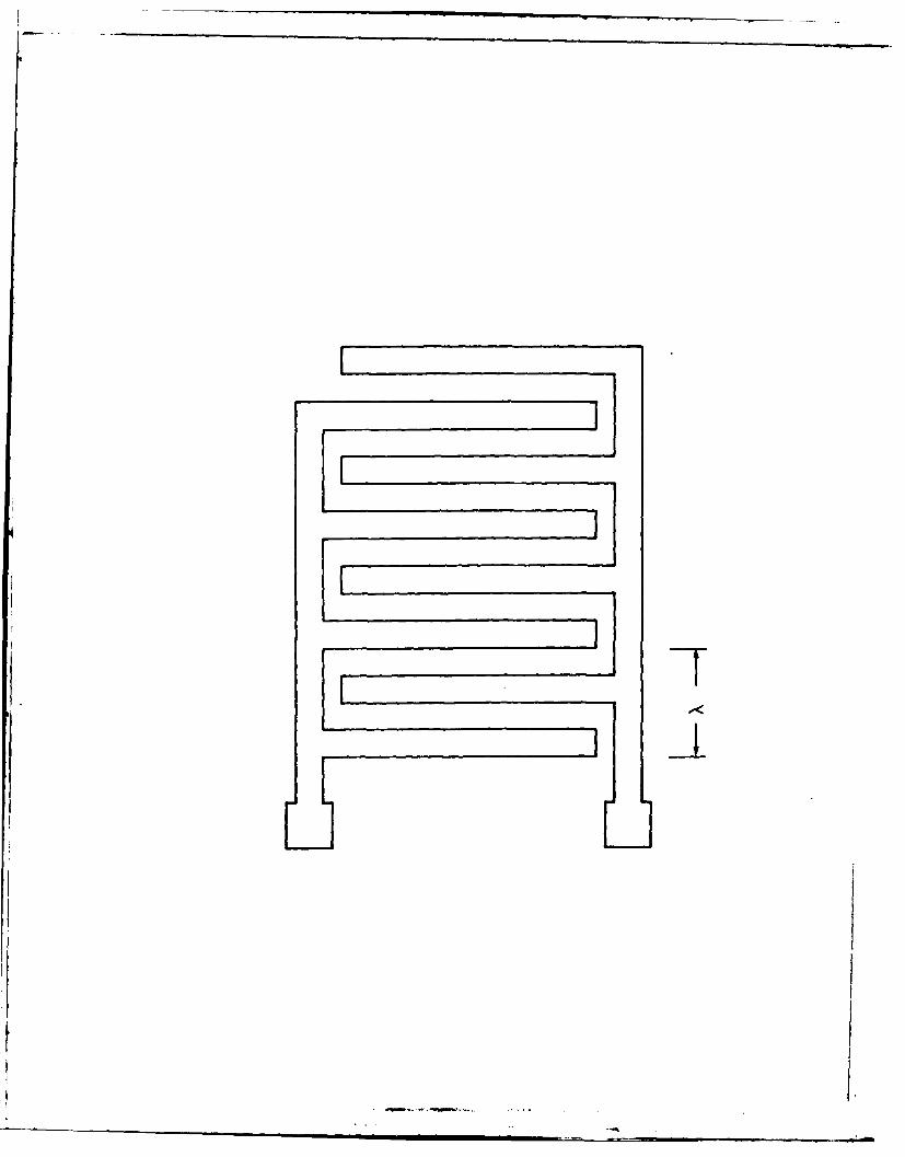
The interdigital transducer (IDT) [1] is the most efficient means of
exciting and detecting surface acoustic waves (SAW) on piezoelectric media.
It consists of a series of metal strips where alternate strips are inter-
connected as shown in figure Ia. The upper limit on the operating frequency
of a SAW device is determined by the capability of the photolithographic
technique being used to define the interdigital transducer. A configuration
employing a two layer transducer on lithium niobate has been used to double
the frequency range for LiNbO 3 SAW devices [2]. Herein we describe a technique
for doubling the operating frequency for use in the ZnO-on-silicon layered
device configuration.
The proposed transducer structure is shown in figure lb and is referred
to as the "single phase" structure (3]. The metal widths and spacings for the
•ingle phase structure are X/2 (where X = wavelength of the SAW) while the
metal widths and spacings for the conventional IDT structure are A/4. Thus,
for a given photolithographic limit, one can obtain twice the operating fre-
quency with the single phase structure as opposed to the IDT structure. It
is important to note that a single phase transducer in the form of a grating
[4], as shown in figure lc, will improve device yields. The yields improve
because electrical shorts between fingers or a break in a finger will alter
just a small portion of the transducer's active region.
A Rayleigh mode single phase transducer delay line has been constructed
in the ZnO/SiO 2/Si configuration. The Rayleigh waves propagate in the <100>
direction on a (100) cut 7 Q-cm n-silicon substrate. A 0.12 pm SiO 2 film
thermally grown on the silicon substrate is covered with a 2.6 pm thick ZnO
film deposited by rf sputtering. The transducers consist of 20 aluminum

-3-
fingers of equal width and gap (22.9om) located on top of the ZnO, with
an aluminum underlay at the ZnO-SiO 2 interface. The SAW acoustic beamwidth
is Imm and the center-to-center transducer spacing is 12.7mm. Both input
and output transducers were tuned with series inductors and there is a con-
volver gate located between the transducers.
Figure 2 shows the two port insertion loss for the Rayleigh device
plotted as a function of frequency. The insertion loss at the synchronous
frequency, f = 94MHZ, iH 25db. This loss value is comparable to that achiev-0
ed with other MZOS RayI-irh delay lines (5-81. However it was found that the
background signal level, due to direct electromagnetic coupling between the
single phase transducers, is only 25db below the response peak. In the IDT
structure this direct coupling is often reduced by use of a balanced drive.
When using the single phase structure we have found that one can make use
of a balanced drive by placing two single phase delay lines in parallel as
shown in figure 3. We will refer to this as the separate comb configuration.
In figure 4 the two port insertion loss for a balanced separate comb
Rayleigh device is shown. All the parameters are the same as the previously
described Rayleigh device except that the beamwidth is now 2mm and there are
two convolver gates, one between each half of the transducers. The synchronous
insertion loss is 22db and the background noise level is now 60db below the
peak transduction. It should be noted that this structure is similar in
complexity to a convolver configuration used to obtain self-convolution
suppression [91.
In addition to the Rayleinh device, a Sezawa mode balanced separate
comb transducer delay line was also constructed. Here the parameters are

the same as for the balanced separate comb Rayleigh device except that the
ZnO film is now 10 pm thick, and is deposited by rf magnetron sputtering [101.
The two port insertion loss for the Sezawa device is plotted as a function
of frequency in figure 5. The insertion loss at the synchronous frequency,
f 0= 114.5MHZ, is 18db, a value comparable with other MZOS Sezawa delay
lines [11-12].
The operation of the single phase and separate comb transducers can be
examined using a normal mode approach 113] in which one compares the radia-
tion resistance, Ra, and the static capacitance, Cs, of the single phase
and balanced separate comb structures to that of the conventional IDT
structure. The first comparison made is between a single phase transducer
of N fingers and an IDT of N finger pairs that is driven unbalanced. The
mark to space ratio is taken as unity for both transducers and they have the
same beamwidth. For the single phase structure the radiation resistance is
found to be one-half, and the static capacitance is twice that of the un-
balanced IDT. Therefore the electrical fractional bandwidth, given by
A 0xf=f 2f oC R , is the same for the single phase structure and the IDT
structure driven unbalanced. The second comparison is between a balanced
separate comb transducer (with N fingers in each parallel half of the trans-
ducer) and an IDT of N finger pairs operated with balanced drive. Again
the mark to space ratio is unity in both transducers but now the total
beamwidth of the balanced separate comb was taken to be twice that of the IDT.
For the balanced separate comb transducer the radiation resistance is one-half
and the static capacitance is twice that of the IOT structure driven balanced.
Therefore the electrical fractional bandwidth is the same for the balanced
separate comb and balanced IDT structures.

-5-
In conclusion we have demonstrated a technique for doubling the operat-
ing frequency for both MZOS Rayleigh and Sezawa mode transducers without an
increase in conversion loss, or in the amount of direct coupling. In
addition for devices constructed for a particular frequency, the device
yields will be improved with use of the single phase grating structure.
The improvement is due not only to increased metal widths and spacings,
but also because shorts between transducer fingers or a break in a finger
should have little effect on the performance of the transducer.
This work was supported by the Air Force Office of Scientific Research
under Grant No. AFOSR-77-3304, National Science Foundation Grant No. ENG 76-11229,
and NSF-MRL Grant No. DMR 77-23798.

-6-
REFERENCES
[I] R. M. White and F. W. Volter, "Direct Piezoelectric Coupling to Surface
Elastic Waves", Appl. Phys. Lett., vol. 26, pp. 314-316, 1965.
(2] H. Harada and R. L. Gunshor, "Two-Layer Interdigital Transducer forAcoustic-Surface-Wave Devices", Elec. Lett., vol. 12, pp. 82-84, 1976.
[31 L. A. Coldren, "Effect of Bias Field in a Zinc-Oxide-on-Silicon AcousticConvolver", Appl. Phys. Lett., vol. 25, pp. 473-475, 1974.
[4] R. M. Artz, E. Salzmann, and K. Nransfeld, "Elastic Surface Waves in
Quartz at 316 MHZ', Appl. Phys. Lett., vol. 10, pp. 165-167, 1967.
[51 B. T. Khuri-Yakub and G. S. Kino, "A Monolithic Zinc-Oxide-on-SiliconConvolver", Appi. Phys. Lett., vol. 25, pp. 188-190, 1974.
[61 K. L. Davis, "Storage of Optical Patterns in a Zinc-Oxide-on-SiliconSurface Wave Convolver", Appl. Phys. Lett., vol. 26, pp. 143-145, 1975.
[7] J. K. Elliott, R. L. Gunshor, R. F. Pierret, and K. L. Davis,"Zinc Oxide-Silicon Monolithic Acoustic Surface Wave Optical ImageScanner", Appl. Phys. Lett., vol. 27, pp. 179-181, 1975.
[8] M. R. Melloch, R. L. Gunshor, C. L. Liu, and R. F. Pierret, "InterfaceTransduction in the ZnO-SiO 2 -Si Surface Acoustic Wave Device Configura-
tion", Appl. Phys. Lett., vol. 37, PP. 147-150, 1980.
[9] I. Yao, "High Performance Elastic Convolver with Parabolic Horns",1980 Ultrason. Symp. Proc., pp. 37-42.
[10] T. Shiosaki, "High-Speed Fabrication of High-Quality Sputtered ZnOThin-Films for BulL, and Surface Wave Applications", 1978 Ultrason.Symp. Proc., pp. 100-110.
[i1 J. K. Elliott, R. L. Gunshor, R. F. Pierret, and A. R. Day, "A Widebaod
SAW Convolver Utilizing Sezawa Waves in the Metal-ZnO-SiO 2-Si Configura-
tion", Appl. Phys. Lett., vol. 32, pp. 515-516, 1978.
[121 F. C. Lo, R. L. Gunshor, and R. F. Pierret,"Monolithic (ZnO) Sezawa-Mode pn-Diode-Array Memory Correlator", Appl. Phys. Lett., vol. 34,
pp. 725-726, 1979.
[13] G. S. Kino and R. S. Wagers, "Theory of Interdigital Couplers on Non-piezoelectric Substrates", J. Appl. Phys., vol. 44, pp. 1480-1488, 1973.

-7-
FIGURE CAPTIONS
]a Conventional interdigital transducer configuration
lb Single phase transducer configuration
ic Single phase grating transducer configuration
2. Frequency response of single phase transducer Rayleigh device
3. Separate comb transducer device configuration
4. Frequency response of separate comb transducer Rayleigh device
5. Frequency response of separate comb transducer Sezawa device
t I
-A-
t) ~~~

I ____ II ____ I1 '7
_____'-I
t B S
I - - ---- ,---- .--.--

I ____ II ____ II ____
I _______________________________________________________________

LA
zwU03
LL.
0
aA CD
(SP) SSO1 NOIAS~3SNI

~~1I II II II II I
I I 1Z>-I Iz-I
L----------------------i-Jz
wI-
ID
LIJ
-J0
z0
I II I
I II II II II I
m

zit'
LLJ
00
fm 00
(SP) SSOI NOI1li3SNI

Ln
zwi
0x
C) C CD
(SP) SSO1 NOI183lSNI -

I 60
200
60
5±. 1. .0
A/50
40
85 90 95 00 105 700 15 Q0 1?5
FIG. 3. Insertion loss for transmission through a reflector array consisting
of 400 shorted Cr/Au strips.'0 sO 10 ' 000 ", 0 "0
ture coefficient of frequency was found to be - 31 ppm/'Cnear room temperature. This agrees with theoretical re-
Isults" which also predict that a proper choice of the SiO2Ilayer thickness could result in a temperature-compensated~device.'0 , ' In conclusion, surface acoustic wave resonators incor-
, ." ' . porating a ZnO-on-Si layered structure have been construct-
ed and characterized. The excellent performance of the0 ,0 shorted Cr/Au configuration, in particular, indicates that it
is feasible to fabricate moderate-Q VHF-UHF resonators di-
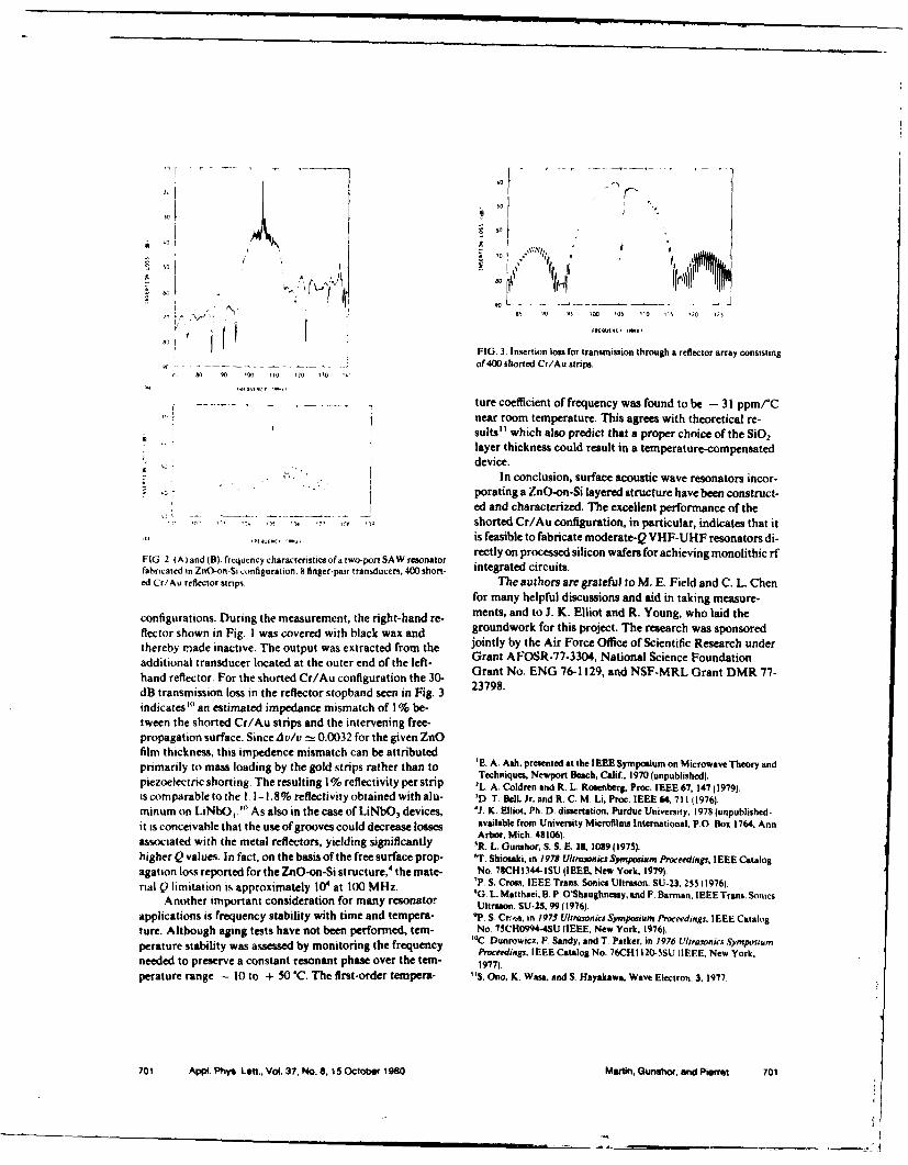
FIG, 2 (A) and (B): frequency characteristics of & two-port SAW resonator rectly on processed silicon wafers forachieving monolithic ffabricated in ZnO-on-Si configuration. 8 finger-pair transducers, 400 short- integrated circuits.ed Cr/Au reflector strips. The authors are grateful to M. E. Field and C. L. Chen
for many helpful discussions and aid in taking measure-
configurations. During the measurement, the right-hand re- ments, and to J. K. Elliot and R. Young, who laid the
flector shown in Fig. I was covered with black wax and groundwork for this project. The research was sponsored
thereby made inactive. The output was extracted from the jointly by the Air Force Office of Scientific Research under
additional transducer located at the outer end of the left- Grant AFOSR-77-3304, National Science Foundation
hand reflector. For the shorted Cr/Au configuration the 30- Grant No. ENG 76-1129, and NSF-MRL Grant DMR 77-
dB transmission loss in the reflector stopband seen in Fig. 3 23798.
indicates"' an estimated impedance mismatch of 1% be-tween the shorted Cr/Au strips and the intervening free-propagation surface. Since Aviv -- 0.0032 for the given ZnOfilm thickness, this impedence mismatch can be attributedprimarily to mass loading by the gold strips rather than to 'E. A. Ash, presented at the IEEE Symposium on Microwave Theory and
Techniques, Newport Beach, Calif.. 1970 (unpublished).piezoelectric shorting. The resulting I % reflectivity per strip 2L. A. Coldren and R. L. Romnberg, Proc. IEEE 67, 147 (19791,is comparable to the 1. 1-1.8% reflectivity obtained with alu- 'D. T. Bell, Jr. and R. C. M. Li, Proc. IEEE 64. 711 (1976).minum on LiNbO. 'o As also in the case of LiNbO3 devices, '3. K. Elliot, Ph. 0, dissertation, Purdue University, 1978 (unpublished-it is conceivable that the use of grooves could decrease losses available from University Microfilms International, P.O. Box 1764, Ann
Arbor, Mich. 481061.associated with the metal reflectors, yielding significantly 'R. L. Ounshor, S. S. E. Ilk 106911975).higher Q values. In fact, on the basis of the free surface prop- 'T. Shioaki, in 1978 Ultr sonkc Symposium Piceedingr, IEEE Catalogagation loss reported for the ZnO-on-Si structure," 00e mate- No. 78CH 1344-ISU (IEEE, New York, 19791.ral Q limitation is approximately 10 at 100 MHz 'P. S. Cross IEEE Trans. Sonics Ultrason. SU-23, 255 (19761.
10, L. Matthaei, B P. O'Shaughneasy. and F. Barman. IEEE Trans. Sonic$Another important consideration for many resonator Ulton. SU-25, " (1976).
applications is frequency stability with time and tempera- 'P. S. Cross, in 1975 lltrsonics Symposium Phtcerdinp, IEEE Catalogture. Although aging tests have not been performed, tern- No. 75CH0994-4SU (IEEE, New York, 1976).perature stability was assessed by monitoring the frequency 'C. Dunrowicz, F. Sandy, and T. Patker, in 1976 Ultrasonics Symposium
Prryeedings, IEEE Catalog No. 76CHI 120-5SU (IEEE, New York,needed to preserve a constant resonant phase over the tern- 1977).perature range - 10 to + 50 *C. The first-order tempera- "S. Ono. K. Wasa, and S. Hayakawa, Wave Electron. 3, 1977.
701 Appl. Phys. Lelt.. Vol. 37, No. , 15 Ottober 1980 Malni, Gunaho . Id Pie 701
"wt I..
FIG. 3. Insertion loss for transmission through a reflector array consisting
-A of400 shorted Cr/Au strips.s, o ' oo 110 120 "D ,
ture coefficient of frequency was found to be - 31 ppmtCnear room temperature. This agrees with theoretical re-sults " which also predict that a proper choice of the SiO 2
5 1 layer thickness could result in a temperature-compensatedI device.
In conclusion, surface acoustic wave resonators incor-porating a ZnO-on-Si layered structure have been construct-ed and characterized. The excellent performance of the
,, shorted Cr/Au configuration, in particular, indicates that itis feasible to fabricate moderate-Q VHF-UHF resonators di-
FIG. 2 (A) and (B) frequency characteristics ofa two-port SAW resonator rectly on processed silicon wafers for achieving monolithic rffabricated in ZnO-on-Si configuration. 8 finger-pair transducers, 400 short- integrated circuits.ed Cr/Au reflector strips. The authors are grateful to M. E. Field and C. L. Chen
for many helpful discussions and aid in taking measure-
configurations. During the measurement, the right-hand re- ments, and to J. K. Elliot and R. Young, who laid theflector shown in Fig. I was covered with black wax and groundwork for this project. The research was sponsoredthereby made inactive. The output was extracted from the jointly by the Air Force Office of Scientific Research underadditional transducer located at the outer end of the left- Grant AFOSR-77-3304, National Science Foundationhand reflector. For the shorted Cr/Au configuration the 30- Grant No. ENG 76-1129, and NSF-MRL Grant DMR 77-dB transmission loss in the reflector stopband seen in Fig. 3 23798.
indicates ". an estimated impedance mismatch of 1% be-tween the shorted Cr/Au strips and the intervening free-propagation surface. Since Av/v e 0.0032 for the given ZnOfilm thickness, this impedence mismatch can be attributedprimarily to mass loading by the gold strips rather than to 'E. A. Ash, presented at the IEEE Symposium on Microwave Theory and
Techniques, Newport Beach, Calif., 1970 (unpublished.piezoelectric shorting. The resulting 1% reflectivity per strip ZL. A. Coldren and R. L. Roaenberg, Proc. IEEE 67, 14711979).is comparable to the 1. 1- 1. 8% reflectivity obtained with alu- 'D. T Bell, Jr, and R. C. M, Li, Proc. IEEE 64, 711 (1976).minum on LiNbO,.' 0 As also in the case of LiNbO 3 devices, 41. K. Elliot, Ph. D. dissertation. Purdue University, 1978 (unpublished.it is conceivable that the use of grooves could decrease losses available from University Microfilms International. P.O. Box 1764. AnnArbor, Mich. 48106).associated with the metal reflectors, yielding significantly Rb. cunshor, S. S. E. 13, 10g9(1973).higher Q values. In fact, on the basis of the free surface prop- IT. Shiosaki, in 1978 Ultrionics Symposium Proceedings, IEEE Catalogagation loss reported for the ZnO-on-Si structure," the mate- No. 78CH 1344-ISU (IEEE, New York, 1979).rial Q limitation is approximately 104 at 100 MHz. 'P. S. Cross, IEEE Trans. Sonics Ultrason. SU-23. 255 (1976).
'G. L. Matthaei, B. P. O'Shaughnessyand F. Barman. IEEETrans. SonicsAnother important consideration for many resonator Ultrason. SU-25, 99 (1976).
applications is frequency stability with time and tempera- 'P. S. Cr.s, in 1975 Ultrasonics Symposium Proceedings, IEEE Catalogture. Although aging tests have not been performed, tern- No. 75CH0994-45U (IEEE, New York. 1976).perature stability was assessed by monitoring the frequency 'C Dunrowicz, F. Sandy, and T. Paiker, in 1976 Ultrasonics SymposiumProceedings, IEEE Catalog No. 76CH1 120-5SU (IEEE, New York,needed to preserve a constant resonant phase over the tern- 1977).perature range - 10 to + 50 *C. The first-order tempera- "S. Ono, K. Wasa. and S. Hayakawa, Wave Electron. 3, 1977.
701 App. Phys. Lett., Vol. 37, No. 8.,15 October 1980 Martin, Gunshor. and Plierrt 701

APPENDIX C
HIGH Q, TEM9PERATURE STABLE ZnO-on"SILICJN SAW RESONATORS
S. J. Martin, R. L. Gunshot and R. F. Pierret
School of ELectrical. Engineering, Purdue University
West Lafayette, Indiana 47907
ABSTRACT strips, as welt as grooves etched in the 2nG layer,
to fore efficient distributed reflectors and to
A monolitbic SAW ZnO/Si0 2 /Si resn)nator device is reali ze low values o f insertion toss at the
reported and severaL configurations for reflector resonant frequency. In section if we discuss thp
structures are described. The twe-port resonators resutts obtained with aluminum and chrome/goLd re-
are found to exhibit Q-vatues i n the 2,000 to flector strips, while section III consider chemi-
1 0,000 range depending upon the use of metallic or catty etched groove devices. The results of temn-
etched reflector arrays. Temperatu.re compensation perature compensation experiments are discussed
through the use of thick thermal oxide Jayers is section IV.
also demonstrated.
II. METAL REFLECTOR DEEvCES
1. Introduction
Figure 1 displays a ZnO-on-SiLicon resonator
Surface acoustic wave resonators fabricated on configuration utilizing metal strip reflector elm-
single crystals of ijuartz or LiNbO 3 have demon- ments. In fabricating the device a 0.1wii-thick-
,Gtrated applicab iity as narrow band filters and as Sbo? Layer is thermally grown on the (111) cut sit-
frequency control. elements in oscillators. The icon substrate and covered with a 0.lpm vacuum-
high value of eLectromechanical coupling make deposited aluminum Layer. The aluminum i.yer both
LiNbO 3 attraC'1va, while Low material oss and tem- enhances AV/V and avoids electroacruistic attenua-
perature stability favor quartz. In this paper we tion caused by piezoeLectric routing to mobi~e
dissuss a passive adaptation of SAW resonator tech- carriers in the semiconductor. 4A 1.6wm Znil film is
noLogy to the ZoO-on-Si Layered configuration. 12 nest deposited by employing rf-magnetron sputter-
Tfi" motivation for using this cart iguration Lies in
tr iibIlli of zonstructing VHF-UHF resonators
d ir e c tL y on prectesseo silicon wafers for achieving ~ $.f -I
monvLit'iic rf integrated circuits. Moreover, reso- V"K TO -
nators fabricated in the Layered configuration can \
be made competitive with LiNbO relative to Q and '\ \' "-S
insertion .oss; furthermore, they csn be made tern- -a-
cierature siabce to a degree comoarabLe to ST
quartz.
The electromecranicdI coupling strength, which Fig. 1 ZrO-on-Si SAW two-port resni tor with metal
depe'd s on thm e iezoetectric ZnO film thickness in strip reflectors. External transducer per-
ti~etayredtrictreis ntemedateto hatof its measurement of transe'-siion throuiis~e ayeel t'itum, s iteredateto hat ofreflector array, The reft. *or secoaration
quartz al, L , N ). 3' is permits he use of metal anO beamwidth arv 3O-
To Apr1ear in the Proceedings of the 1980 IEEE Ultrasonics Sympisiun

ing. The top metallization pattern is formed from 0l0CE 4(FLICJIRS
either aluminum or chrome gold with interdigital
transducers and reflectors being defined in a sin-
gle photolithographic step. Two port resonators
having a sinae Longitudinal mode were fabricated
with isolated aluminum, isolated Cr/Au, and shorted - to
Cr/Au refLector strips spaced X/2 apart. In order
to couple optimally to the standing wave in the till, .
Lavity, the following spacing between transducer 'iiS.
finger centers and the reflector array edge is re-quired: Fig. 3 ZnO-on-Si SAW two-port rsonator w'th
etched groove/ridge reflectors. The re-
flector separation and beamwidth are 305.
[n/2 + 1/4) x0 for isolated Cr/Au or Figure 2 shows the two port transmission charac-
shorted Cr/Au reflectors teristics of a resonator using 8 f irer-pair trans-
d = ducers and 400 shorted Cr/Au ref ec,'r strips per
n/2)x 0 for isolated al reflectors. reflector array.6
From measurements n4 transmssior,
through the reflector array the reitectivity per
strip is estimated at 1%. Since AV/V - 0.0032 fr
where %0 is the resonant wavelength and n is an in- the ZnO film thickness indicated, tre dominant re
teger. Of the three reflector confiqurations exam- fLection mechanism is concluded to t- mass Loading.
ined, the weakest reflections were observed with The Loaded 0 of this device is 2500. if the rnpu'
the aluminum array, while the strongest reflections and output are decoupled from tre 5O0i tine ts.
were obtained from the shorted Cr/Au array. resulting unloaded Q is 3100. ALso, since the dom-
_0 inant loss mechanism is conductive Loss in the me-
tat strips, the efficiency of the Cr/Au reflector
20 array is greater for fil, thicknesses less than
that corresponding to the maximum AVIV.
-0
40 Ill. ETCHED GROOVE DEVICES
50 To eliminate losses associated with the conduc-
tivity of metal reflectors, resonators were subse-
60 [ quenitly fabricated using grooves chemically etchediin the ZnO layer, (Fig. 3). The fabrication is
70 identical to that of the metal strip resonator
described previously up to the point of the top
0 j metallization pattern. After sputtering the ZnO
film, a top aluminum layer is evaporated from whict,90
70 80 90 100 110 120 130 140 interdigital transducers and a ref lrtor array mask
for subsequent etching of grooves are formed. At.FRtQUtNCi (MKz)
alkaline etch is used to define the metallization
Fig. 2 Frequency characteristics of a two-port pattern without damaging the ZnO layer. The region
ZnO-on-si SAW resonator using Cr/Au reflec- between reflector arrays is then orctected with
tor strips. 8 finger-pair transducers, 400
shorted Cr/Au reflector strips. photoresist while a dilute solutiop of HNO removes

ZnO between the masking strips of aluminum. Final-
Ly, the aluminum masking strips and the photoresist
used to protect the transducer region are removed.
The remaining ZnO ridges act as effective topologi-
cal surface wave reflectors. This is a result of
the velocity perturbation associated with the vary-
ing InO thilcness, as welt as the perturbation as- "
sociated with the geometric discontinuity itself.7
-
In contrast to etched groove reflectors formed in
single crystals, the velocity increases with
moderate groove depths in the ZnO layer due to the
decreasing average thickness of the slower ZnO
layer. Shimizu and Takeuchi8
have shown that the Fig. 5 Expanded view of reso. ance peak in Fig. 4
effect of groove wall sloping--which is to be ex- showing multiple transverse mode peaks.
petted with chemically etched grooves--has a minor
effect on the reflection magnitude at the grating only on the normalized groove depth (h/x) but also
fun.amental. on the ratio of the groove depth to the total ZnO
Figure 4 exhibits the two port transmission thickness.
characteristics of a resonator employing 8 finger- The Loaded Q of the etched device is measured at
pair transducers and 350 etched grooves per reflec- 6400. The insertion Loss of 9 dB at the center
tor. The groove depth is 0.68um, a distance nearly frequency indicates an unloaded Q of nearly 10,000.
half way through the 1.55um ZnO layer. From This compares favorably with values reported for
transmission measurements on test structures with both LiNbO 3 and quartz devices. The higher Q-value
various groove depths the reflectivity per groove obtained for the configuration shown in Fig. 3 com-
is estimated at 1.26% for the groove depth cited, pared to the metal strip configuration (Fig. 1) can
The reflertivity per groove is found to depend not be attributed to severat factors. The conductive
Losses in the reflector array have been eliminated,
while at the same time we have reduced the trans-
ducer reflections by using aluminum rather than
Cr/Au. In addition, we anticipate some reduction
in diffraction losses of the 30. wide structure due
30 to waveguiding. That is, in etching the grooves in
the ZnO layer we have simultaneously etched the ZnO
outside the beamwidth to the level of the groove
depth. The region containing the "ridge" reftec-8 so
tors, having a greater average ZnO thickness,
• sc therefore has a velocity characteristic lower than
that found outside the beamwidth. The result is a
greater Lateral confinement of the beam - a possi-* bLe explanation for the number and prominence of
transverse mode peaks in Fig. 5.10
It is significant to observe that the measured
9 95 Igo 11 110 Ili 155 is IS Q-value places an upper limit oi the material
"-K, (m') losses present in the structure of approximately
Fig. 4 Frequency characteristics of a two-port 1.2 dB/cm at 109 MHz. This value is consistentZnO-on-Si resonator utilizing etched groovereflectors. 8 finger-pair transducers, 350 with measurements of free surface propagation loss
grooves etched .68um into 1.55um (nO layer, in ZnO/Si devices reported by Hicleernell.1 1
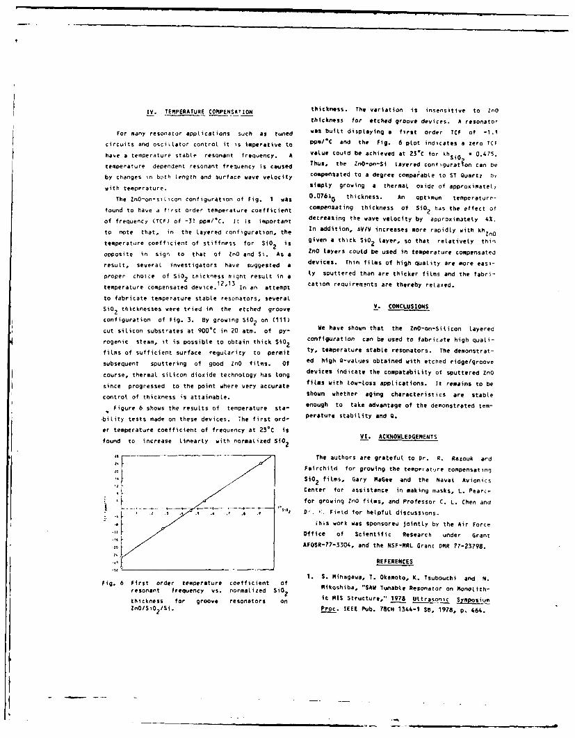
IV. TEMPERATURE COMPENSATION thickness. The variation is insensitive to InO
thickness for etched groove devices. A resonator
For many resonator applications such as tuned was built displaying a first order TCF of -1.1
circuits and oscillator control it is imperative to ppmlC and the Fig. 6 plot indicates a zero TCF
have a temperature stable resonant frequency. A value could be achieved at 23*C for kh - 0.475.
temperature dependent resonant frequency is caused Thus, the ZnO-on-Si layered configuration can te
by changes in both length and surface wave velocity compensated to a degree comparable to ST Quartz bywith temperature. simply growing a thermal oxide of approximatet,
The ZnO-on-silicon configuration of Fig. 1 was 0.076x0 thickness. An optimum temperature-
found to have a first order temperature coefficient compensating thickness of SiO 2 has the effect of
of frequency (TCF) of -31 ppm/4C. It is important decreasing the wave velocity by approximately 4%.
to note that, in the layered configuration, the In addition, 6V/V increases more rapidly with khzn0
temperature coefficient of stiffness for SiO 2 is given a thick Si 2 layer, so that relatively thin
opposite in sign to that of mnO and Si. As a ZnO layers could be used in temperature compensated
result, several investigators have suggested a devices. Thin films of high Quality are more easi-
proper choice of si 2 tnickness Might result in a ly sputtered than are thicker films and the fabri-
temperature compensated device.1 2
,1 3
In an attempt cation requirements are thereby relaxed.
to fabricate temperature stable resonators, several
SiO 2 thicknesses were tried in the etched groove V. CONCLUSIONS
configuration of Fig. 3. By growing SiO 2 on (111)
cut silicon substrates at 900*C in 20 atm. of py- We have shown that the ZnO-on-Silicon layered
rogenic steam, it is possible to obtain thick SiO 2 configuration can be used to fabricate high quali-films of sufficient surface regularity to permit ty, temperature stable resonators. The demonstrat-
subsequent sputtering of good ZnO films. Of ed high G-values obtained with etched ridge/groove
course, thermal silicon dioxide technology has long devices indicate the compatability of sputtered ZnO
since progressed to the point where very accurate films with Low-loss applications. It remains to be
control of thickness is attainable, shown whether aging characteristics are stable
Figure 6 shows the results of temperature sta- enough to take advantage of the demonstrated tem-
bility tests made on these devices. The first ord- perature stability and Q.
er temperature coefficient of frequency at 230C isVI. ACKNOWLEDGEMENTS
found to increase linearly with normalized SiO 2
1 The authors are grateful to Dr. R. Razouk and
Fairchild for growing the temoeiature compensating
SO 2 films, Gary MaGee and the Naval Avionics
Center for assistance in making masks, L. Pearcefor growing nO films, and Professor C. L. Chen and
Dr. ,r Field for helpful discussions.
.hiS work was sponsorej jointly by the Air Force
.4 Office of Scientific Research under Grant
AFOSR-77-3304, and the NSF-MRL Grant OMR 77-23?98.
REFERENCES
1. S. Minagawa, T. Okamoto, K. Tsubouchi and N.Fig. 6 First order temperature coefficient ofMksha, AWTnbeRoatrnMnlih
resonant frequency vs. normalized SiO 2 Mikoshiba, "SAW Tunable Resonator on onolith-
thickness for groove resonators on it MIS Structure," 1978 Ultrasonic im. IufZnO/SiO 2 /Si. Proc. IEEE Pub. 78CH 1344-1 SO, 1978, p. 464.

2. M. R. MeLLoct, R. L. Gunshor, C. L. Liu and R. 8. N. Shimizu and 14. Takeuchi, "Theoretical Stu-
F. Pierret, "Interface Transduction in the dies of the Energy Storage Effects and the
ZnO-SiO 2-Si Surface Acoustic Wave Device Con- Second Harmonic Responses of SAW Reflection
figuration," Appl. Phys. Lett., vol. 37, no. Gratings," 1979 Ultrasonic symposium Proc.,
2, p. 147, July 15, 1980. IEEE Pub. 99CH 1482-9, 1979, p. 932.
3. J. K. Elliott, "Zinc Oxide on Silicon Surface 9. E. J. Staples, J. S. Schoenwald, R. C. Rosen-
Acoustic Wave Devices for Signal Processing febo, and C. S. Hartmann, "UHF Surface Acous-
and Frequency Control," Ph.D. dissertation, tic Wave Resonators," 1974 Ultrasonic
Purdue University, 1978 (unpublished - avail- Symposium Proc., iEEE Pub. 74CHO 896-ISU,
able from University Microfilms International, 1974, p. 245.
P.O. Box 1764, Ann Arbor, MI 48106).
4. R. L. Gunshor, "The Interaction Between Sem- 10. M. A. Haus, "Modes in SAW Grating Resonators,"
iconductors and Acoustic Surface Waves - A Re- !L. AppL. Phys., vol. 48, no. 12, p. 4955, Dec.
view," S.S.E. 18 1089 (1975). 1977.
5. T. Shiosaki, "High-Speed Fabrication of High- 11. F. S. HickernelL, "An Optical Measure of the
Quality Sputtered ZnO Thin-Films for Bulk and Acoustic Quality of Zinc Oxide Thin Films,"
Surface Wave Applications," 1978 Ultrasonic 1979 Ultrasonic Symposium Proc., IEEE Pub.
Symposium Proc., IEEE Pub. 78CH1344-1SU, 1978, 99CH 1482-9, 1979, p. 932.
p. 100.
12. 6. Cambon, E. L. Adler, J. Attal, and W.
6. S. J. Martin, R. L. Gunshor, R. F. Pierret, Shahab, "Temperature Effects on Acoustic Sur-
"Zinc Oxide-on-Silicon Surface Acoustic Wave face Wave Devices on Silicon," 1979 Ultrasonic
Resonators," AppL. Pnys. Letts., vol. 37, no. Symposium Proc., IEEE Pub. 99CH 1482-9, 1979,
8, p. 200, Oct. 15, 1980. p. 637.
7. A. A. Oliner, H. I. Bertoni and R. C. M. Li, "A 13. S. Ono, K. Wasa, S. Hayakawa, "Surface-
Microwave Network Formalism for Acoustic Waves Acoustic-Wave Properties in ZnO-SiO 2 -Si Lay-
in Isotropic Media," Pro. IEEE, vol. 60, pp. ered Structure," Wave ELectronics, vol. 3,
1503, 1972. 1977, pp. 35-49.
-- i mm I1503,I 1972.

DI