Embed Size (px)
Citation preview

www.intelligraphics.com 972-479-1770
Page 1
Datasheet IGX QCA4020
Hardware Module - IGX-RNF1-4020a3-BT
IGX-RNF1-4020a3-BT
»» Ultra Small 802.11n Dual-Band
1Tx1R Wireless + Bluetooth v5.0 +
Zigbee (15.4) IoT Module
This module is an intelligent platform for the Internet of Things (IoT) that contains a low-power Wi-Fi
(802.11 a/b/g/n 1x1), Bluetooth Low Energy (BLE) 5.0 and Zigbee (802.15.4) connectivity protocols along
with SSL, enabling a low-cost, low-complexity system to obtain full-featured internet connectivity and
reliable information exchange.
QCA4020 device contains three processors:
The first processor, an ARM Cortex-M4F@ up to 128MHz is used as the application processor. It
runs the Qualcomm network stack as well as OEM application code. Customer software runs
under an RTOS such as ThreadX or FreeRTOS and so on.
Second processor, an ARM Cortex-M0@64MHz, which is utilized as the connectivity processor for
BLE and 802.15.4 subsystem.
Third processor, CPU which is a dedicated processor to run the Wi-Fi dual-band function.
The IGX-RNF1-4020a3-BT module provides a highly-integrated and flexible platform for developing and
evaluating products and applications based on QCA4020 SoC. IGX-RNF1-4020a3-BT module can be either
used with a development kit for software development or incorporated into OEM products to enable
rapid deployment of Wi-Fi connected system.
KEY FEATURES
IEEE Standards Support, 802.11a, 802.11b, 802.11g, 802.11n, and single-stream 1x1.
Supports 20MHz channel width in 2.4 and 5GHz.
Operate at ISM frequency Band (2.4/5GHz).
Bluetooth Low Energy (BLE) compliant to the SIG v5.0 specification.
www.intelligraphics.com 972-479-1770
Page 2
Datasheet IGX QCA4020
Hardware Module - IGX-RNF1-4020a3-BT
Green TX power-saving mode and Low-power listen mode.
Rich set of GPIOs and interface: I2C, HSUART, UART, SPI, QSPI, SDIO2.0, I2S, JTAG, Sensor ADC
(up to 8 channels, 12bit, 1Mbps), up to 8 PWM optimized for LED lighting applications.
Advanced power management scheme to minimize power dissipation for each use case.
Supports 32Mb NOR flash memory.
Supports on board printed Antenna.
Supporting OS: ThreadX RTOS and FreeRTOS
SPECIFICATIONS
1. Software Specifications
Standards
802.11a;802.11b; 802.11g; 802.11n, 802.11d, 802.11h ,
802.11v
STA, SoftAP Mode, WiFi-Direct, IBSS
11n Features: STBC, LDPC, MLD, MRC, Short GI, AMPDU Rx
and Tx aggregation, AMSDU Rx
Driver Support ThreadX RTOS and FreeRTOS
Security
WEP, WPA-PSK, WPA2-PSK, WPS
Enterprise IEEE 802.1x EAP-TLS
Network Services Support
TCP, UDP, DHCP client/server, BSD Socket, SSL
DNS client/server, SNTP, CoAP Client/server, websocket
HTTP Client/Server, MQTT Client, SSDP, mDNS, IGMP v1/v2
Supported IoT Frameworks Amazon Web Services (AWS) IoT
Microsoft Azure IoT
SDK Features
Concurrent demo SCC/MCC (SoftAP + STA)
Concurrent mode: Wi-Fi direct client + Legacy Station
Sniffer mode with optional filters
Low power listen, Preferred Network Offload (PNO)
Network solicitation offload
ARP Offload
www.intelligraphics.com 972-479-1770
Page 3
Datasheet IGX QCA4020
Hardware Module - IGX-RNF1-4020a3-BT
Wake on Wireless (WoW)
OTA firmware upgrade
Secure Storage and Secure Boot
Support for Green Tx, Store-Recall (Suspend/Resume)
2. Zigbee Function
Standard 802.15.4
Modulation Scheme
O-QPSK
Transmit Output Power
Typical: 0dBm
Receiver Sensitivity
-101dBm
3. Bluetooth Function
Main Chipset
Qualcomm QCA4020
Standard
BT v5.0
Bus Interface
UART
Data Rate
1Mbps, 2Mbps
Modulation Scheme
GFSK
Frequency Range
2.400 ~ 2.4835GHz
Operating Channel 0 ~ 39

www.intelligraphics.com 972-479-1770
Page 4
Datasheet IGX QCA4020
Hardware Module - IGX-RNF1-4020a3-BT
Transmit Output Power
+4 ≤ Output Power ≤ +2dBm; Class 2 Device
Receiver Sensitivity
< 0.1% BLE 1M at -93dBm
4. Wi-Fi Function
Main Chipset Qualcomm QCA4020
Standards IEEE 802.11a; 802.11b; 802.11g; 802.11n
BUS Interface UART
Data Rate
802.11a: 54, 48, 36, 24, 18, 12, 9, 6Mbps
802.11b: 11, 5.5, 2, 1Mbps
802.11g: 54, 48, 36, 24, 18, 12, 9, 6Mbps
802.11n: MCS 0 ~ 7 for HT20
Media Access Control CSMA/CA with ACK
Modulation Technique
802.11a: 64QAM, 16QAM, QPSK, BPSK
802.11b: CCK, DQPSK, DBPSK
802.11g: 64QAM, 16QAM, QPSK, BPSK
802.11n: 64QAM, 16QAM, QPSK, BPSK
Network Architecture Infrastructure mode
Operation Channel
2.4GHz:-
11: (Ch. 1-11) – United States
13: (Ch. 1-13) – Europe
14: (Ch. 1-14) – Japan
5GHz:-
21: USA
19: EU
8: Japan
Frequency Range 802.11bg: 2.400 ~ 2.4835GHz
802.11a: 5.15 ~ 5.85GHz
Transmit Output
Power - single chain
@ant;Tolerance:
± 2dBm @ 2.4GHz; ±2.5dBm @ 5GHz
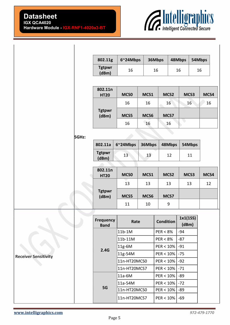
2.4GHz:
802.11b 1Mbps 2Mbps 5.5Mbps 11Mbps
Tgtpwr
(dBm) 17 17 17 17
www.intelligraphics.com 972-479-1770
Page 5
Datasheet IGX QCA4020
Hardware Module - IGX-RNF1-4020a3-BT
802.11g 6~24Mbps 36Mbps 48Mbps 54Mbps
Tgtpwr
(dBm) 16 16 16 16
802.11n
HT20 MCS0 MCS1 MCS2 MCS3 MCS4
Tgtpwr
(dBm)
16 16 16 16 16
MCS5 MCS6 MCS7
16 16 16
5GHz:
802.11a 6~24Mbps 36Mbps 48Mbps 54Mbps
Tgtpwr
(dBm) 13 13 12 11
802.11n
HT20 MCS0 MCS1 MCS2 MCS3 MCS4
Tgtpwr
(dBm)
13 13 13 13 12
MCS5 MCS6 MCS7
11 10 9
Receiver Sensitivity
Frequency
Band
Rate Condition
1x1(1SS)
(dBm)
2.4G
11b-1M PER < 8% -94
11b-11M PER < 8% -87
11g-6M PER < 10% -91
11g-54M PER < 10% -75
11n-HT20MCS0 PER < 10% -92
11n-HT20MCS7 PER < 10% -71
5G
11a-6M PER < 10% -89
11a-54M PER < 10% -72
11n-HT20MCS0 PER < 10% -89
11n-HT20MCS7 PER < 10% -69

www.intelligraphics.com 972-479-1770
Page 6
Datasheet IGX QCA4020
Hardware Module - IGX-RNF1-4020a3-BT
Security WPA, WPA2, WEP 64bit & 128bit, IEEE 802.1X, IEEE 802.11i
5. Common Function
Operating Voltage 3.3 V ± 5% I/O supply voltage
Power Consumption
Mode Average Peak
2.4G 5G 2.4G 5G
TX 315mA 360mA
472mA 540mA RX 302mA 360mA
Standby 70mA
Antenna Type Printed Antenna for WiFi/BT/15.4
RECOMMENDED OPERATION CONDITIONS
Symbol Parameter Min. Type Max. Units
SWREG_IN_WL VDD33_WL WL Internal SWREG supply 3.14 3.3 3.46 V
VDD33_ANT_WL
VDD33_RF_WL
VDD33_XTAL_WL
VDD33_PLL_WL
VDD33_SYNTH_WL
VDD33_USB_WL
WL Analog High Voltage supply 3.14 3.3 3.46 V
DVDD12_WL WL Core Digital supply 1.2 1.26 1.32 V
VDD12_BB_PLL_WL
VDD12_RF_WL
VDD12_SYNTH_WL
WL Core Analog supply
1.2
1.26
1.32
V
DVDDIO_AO_WL
DVDDIO_WL VDDIO_BE
AVDDIO_BE
VIO = 3.3V
3.14
3.3
3.46
V
www.intelligraphics.com 972-479-1770
Page 7
Datasheet IGX QCA4020
Hardware Module - IGX-RNF1-4020a3-BT
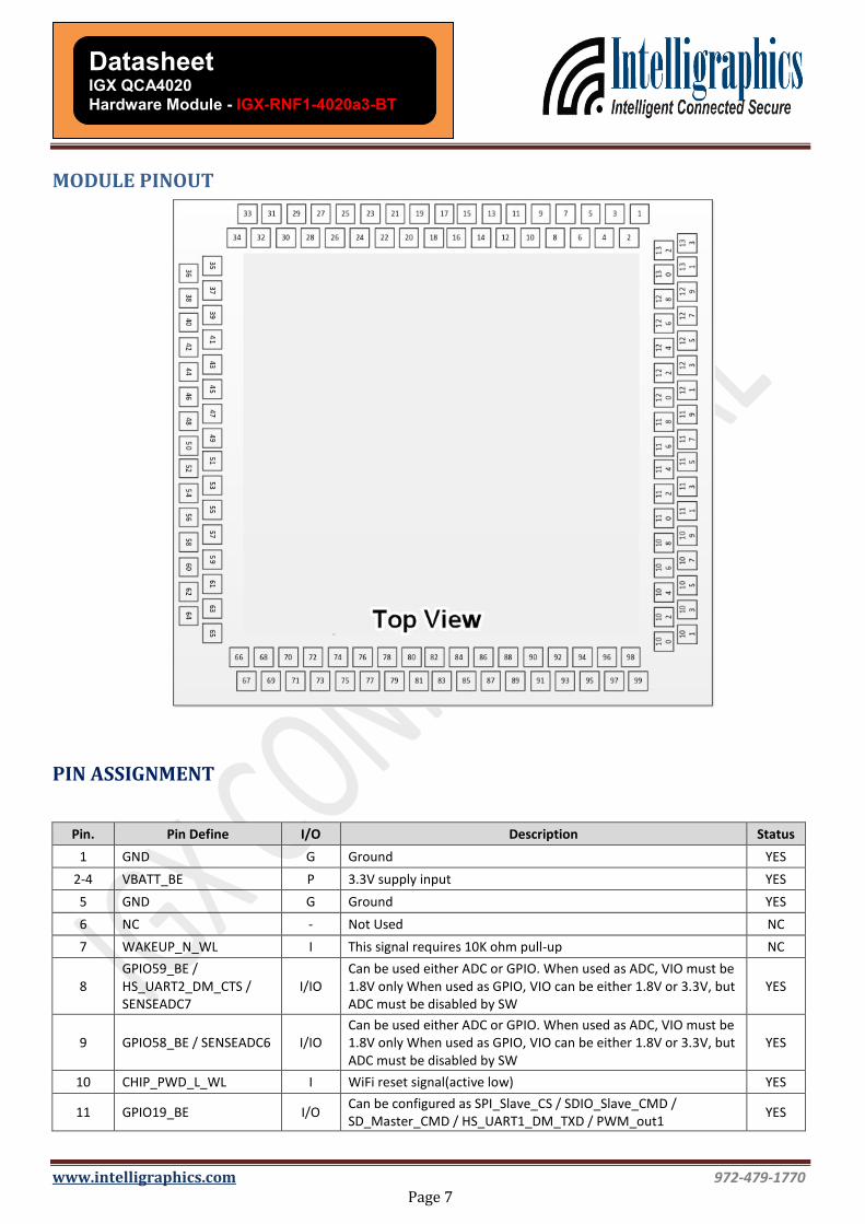
MODULE PINOUT
PIN ASSIGNMENT
Pin. Pin Define I/O Description Status
1 GND G Ground YES
2-4 VBATT_BE P 3.3V supply input YES
5 GND G Ground YES
6 NC - Not Used NC
7 WAKEUP_N_WL I This signal requires 10K ohm pull-up NC
8
GPIO59_BE /
HS_UART2_DM_CTS /
SENSEADC7
I/IO
Can be used either ADC or GPIO. When used as ADC, VIO must be
1.8V only When used as GPIO, VIO can be either 1.8V or 3.3V, but
ADC must be disabled by SW
YES
9 GPIO58_BE / SENSEADC6 I/IO
Can be used either ADC or GPIO. When used as ADC, VIO must be
1.8V only When used as GPIO, VIO can be either 1.8V or 3.3V, but
ADC must be disabled by SW
YES
10 CHIP_PWD_L_WL I WiFi reset signal(active low) YES
11 GPIO19_BE I/O Can be configured as SPI_Slave_CS / SDIO_Slave_CMD /
SD_Master_CMD / HS_UART1_DM_TXD / PWM_out1 YES

www.intelligraphics.com 972-479-1770
Page 8
Datasheet IGX QCA4020
Hardware Module - IGX-RNF1-4020a3-BT
Pin. Pin Define I/O Description Status
12 GPIO57_BE / SENSEADC5 I/IO
Can be used either ADC or GPIO. When used as ADC, VIO must be
1.8V only When used as GPIO, VIO can be either 1.8V or 3.3V, but
ADC must be disabled by SW
YES
13 USB_D+_WL I/O USB differential positive, No Used, NC NC
14 USB_D-_WL I/O USB differential negative, No Used, NC NC
15 GPIO20_BE I/O Can be configured as SPI_Slave_MISO /SDIO_Slave_Data0 /
SD_Master Data0 / HS_UART1 DM_RXD / PWM_Out2 YES
16 GPIO18_BE I/O Can be configured as SPI_Slave_CLK / SDIO_Slave_CLK /
SD_Master_CLK(O) / HS UART1_DM_CTS / PWM_Out_6 YES
17 Bypass_INT_PMU_MSK I No Connect NC
18 GPIO56_BE / SENSEADC4 I/IO
Can be used either ADC or GPIO. When used as ADC, VIO must be
1.8V only When used as GPIO, VIO can be either 1.8V or 3.3V, but
ADC must be disabled by SW
YES
19 GPIO21_BE I/O Can be configured as SDIO_Slave_Data1 / SD_Master Data1(B) /
PWM Out_4 YES
20 GPIO55_BE / SENSEADC3 I/IO
Can be used either ADC or GPIO. When used as ADC, VIO must be
1.8V only When used as GPIO, VIO can be either 1.8V or 3.3V, but
ADC must be disabled by SW
YES
21 GPIO23_BE I/O Can be configured as SPI_Slave_MOSI / SDIO_Slave_Data3 /
SD_Master_Data3(B) / HS_UART1_DM_RFR / PWM Out_5 YES
22 USB20_DM_BE I/O USB differential negative YES
23 USB20_DP_BE I/O USB differential positive YES
24 SENSEADC1_BE I ADC input. If used, VIO must be 1.8V; can be floating if not used YES
25 GPIO54_BE / SENSEADC2 I/IO
Can be used either ADC or GPIO. When used as ADC, VIO must be
1.8V only When used as GPIO, VIO can be either 1.8V or 3.3V, but
ADC must be disabled by SW
YES
26 GPIO22_BE I/O Can be configured as SDIO_Slave_Data2 / SD_Master_Data2(B) /
PWM Out_3 YES
27 SENSEADC0_BE I ADC input. If used, VIO must be 1.8V; can be floating if not used YES
28 GPIO26_BE I/O Can be configured as SPI0_Master_MOSI / JTAG2_BE_TMS YES
29 GPIO24_BE I/O Can be configured as SPI0_Master_CS_N / M0&M4_UART2_RX /
JTAG2_BE_TCK YES
30 GPIO27_BE I/O Can be configured as SPI0_Master_MISO / JTAG2_BE_TDI YES
31 GPIO25_BE I/O Can be configured as SPI0_Master_CLK / M0&M4_UART2_TX /
JTAG2_BE_TDO YES
32 GPIO12_BE I/O Can be configured as PWM Out_0 YES
33 GND G Ground YES
34 NC - Not used NC
35 RTC32K_XTALI I Optional external 32.768KHz crystal input, no connect(or floating) NC
36 RTC32K_XTALO O Optional external 32.768KHz crystal output, no connect(or
floating) NC
37 CHIP_PWD_L_BE I M4 processor and BLE/15.4 Reset signal(active low) YES
38 GND G Ground YES
39-41 VDD11 P 1.1V input supply, host no need to provide NC
42 GND G Ground YES
www.intelligraphics.com 972-479-1770
Page 9
Datasheet IGX QCA4020
Hardware Module - IGX-RNF1-4020a3-BT
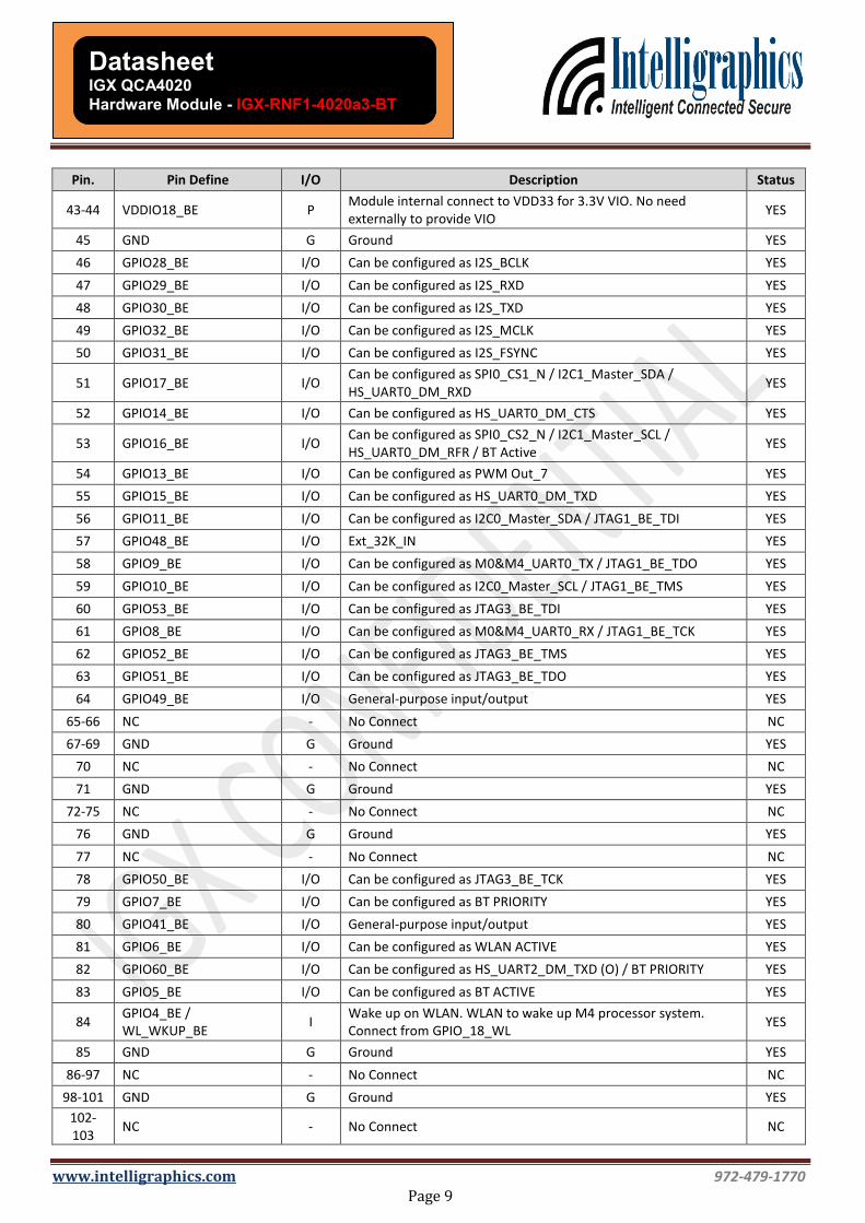
Pin. Pin Define I/O Description Status
43-44 VDDIO18_BE P Module internal connect to VDD33 for 3.3V VIO. No need
externally to provide VIO YES
45 GND G Ground YES
46 GPIO28_BE I/O Can be configured as I2S_BCLK YES
47 GPIO29_BE I/O Can be configured as I2S_RXD YES
48 GPIO30_BE I/O Can be configured as I2S_TXD YES
49 GPIO32_BE I/O Can be configured as I2S_MCLK YES
50 GPIO31_BE I/O Can be configured as I2S_FSYNC YES
51 GPIO17_BE I/O Can be configured as SPI0_CS1_N / I2C1_Master_SDA /
HS_UART0_DM_RXD YES
52 GPIO14_BE I/O Can be configured as HS_UART0_DM_CTS YES
53 GPIO16_BE I/O Can be configured as SPI0_CS2_N / I2C1_Master_SCL /
HS_UART0_DM_RFR / BT Active YES
54 GPIO13_BE I/O Can be configured as PWM Out_7 YES
55 GPIO15_BE I/O Can be configured as HS_UART0_DM_TXD YES
56 GPIO11_BE I/O Can be configured as I2C0_Master_SDA / JTAG1_BE_TDI YES
57 GPIO48_BE I/O Ext_32K_IN YES
58 GPIO9_BE I/O Can be configured as M0&M4_UART0_TX / JTAG1_BE_TDO YES
59 GPIO10_BE I/O Can be configured as I2C0_Master_SCL / JTAG1_BE_TMS YES
60 GPIO53_BE I/O Can be configured as JTAG3_BE_TDI YES
61 GPIO8_BE I/O Can be configured as M0&M4_UART0_RX / JTAG1_BE_TCK YES
62 GPIO52_BE I/O Can be configured as JTAG3_BE_TMS YES
63 GPIO51_BE I/O Can be configured as JTAG3_BE_TDO YES
64 GPIO49_BE I/O General-purpose input/output YES
65-66 NC - No Connect NC
67-69 GND G Ground YES
70 NC - No Connect NC
71 GND G Ground YES
72-75 NC - No Connect NC
76 GND G Ground YES
77 NC - No Connect NC
78 GPIO50_BE I/O Can be configured as JTAG3_BE_TCK YES
79 GPIO7_BE I/O Can be configured as BT PRIORITY YES
80 GPIO41_BE I/O General-purpose input/output YES
81 GPIO6_BE I/O Can be configured as WLAN ACTIVE YES
82 GPIO60_BE I/O Can be configured as HS_UART2_DM_TXD (O) / BT PRIORITY YES
83 GPIO5_BE I/O Can be configured as BT ACTIVE YES
84 GPIO4_BE /
WL_WKUP_BE I
Wake up on WLAN. WLAN to wake up M4 processor system.
Connect from GPIO_18_WL YES
85 GND G Ground YES
86-97 NC - No Connect NC
98-101 GND G Ground YES
102-
103 NC - No Connect NC

www.intelligraphics.com 972-479-1770
Page 10
Datasheet IGX QCA4020
Hardware Module - IGX-RNF1-4020a3-BT
Pin. Pin Define I/O Description Status
104 GND G Ground YES
105-
108 NC - No Connect NC
109 GND G Ground YES
110 EXT_CLKOUT_BE G 1.1Vpp clock output same as crystal frequency NC
111 GND G Ground YES
112-
114 NC - No Connect NC
115 GND G Ground YES
116 NC - No Connect NC
117 PWRDWN_OUT_N - Not used NC
118 NC - No Connected NC
119 GND G Ground YES
120-
123 NC - No Connect NC
124 GND G Ground YES
125 NC - No Connect NC
126 IOT_MODE_EN_WL I This signal requires 10Kohm pull-down. Not used, NC NC
127 GND G Ground YES
128-
129 VDDIO18_WL P
Module internal connect to VDD33 for 3.3V VIO. No need
externally to provide VIO NC
130 GND G Ground YES
131-
133 NC - No Connect NC
*The following signal type is defined:
I: Input; O: Output; I/O: Input/Output; G: Ground; P: Voltage Supply
BOOTSTRAP SIGNALS
Table 2: JTAG mode
GPIO9_BE GPIO25_BE GPIO18_BE Description
0 0 0 No JTAG enabled
0 0 1 JTAG Pins on GPIO[53:50]_BE
0 1 0 JTAG Pins on GPIO[11:8]_BE
0 1 1 JTAG Pins on GPIO[27:24]_BE
1 X X Not Allowed
Table 3: 32.768 KHz Sleep Clock Mode
GPIO21_BE GPIO20_BE Description
0 0 Chip internal LPO
0 1 External Crystal 32.768KHz
www.intelligraphics.com 972-479-1770
Page 11
Datasheet IGX QCA4020
Hardware Module - IGX-RNF1-4020a3-BT
1 0 External 32.768KHz TCXO Clock connected to
GPIO48_BE
1 1 Not Allowed
ELECTRICAL CHARACTERISTICS
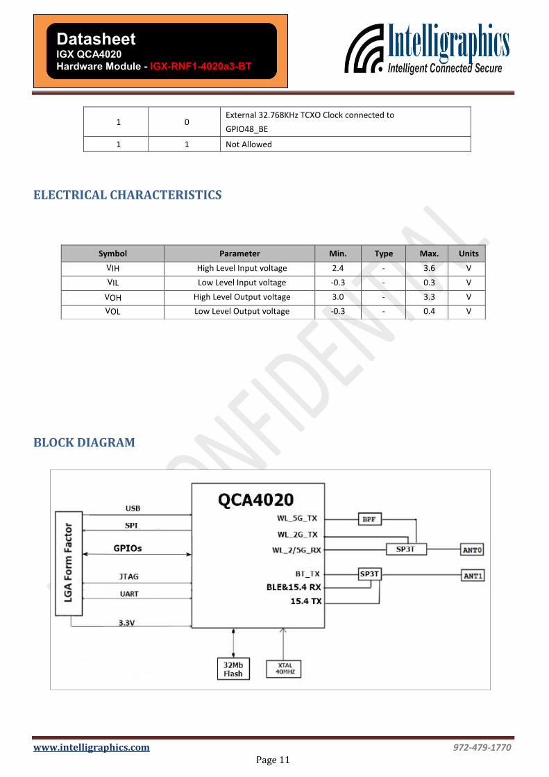
BLOCK DIAGRAM
Symbol Parameter Min. Type Max. Units
VIH High Level Input voltage 2.4 - 3.6 V
VIL Low Level Input voltage -0.3 - 0.3 V
VOH High Level Output voltage 3.0 - 3.3 V
VOL Low Level Output voltage -0.3 - 0.4 V
www.intelligraphics.com 972-479-1770
Page 12
Datasheet IGX QCA4020
Hardware Module - IGX-RNF1-4020a3-BT
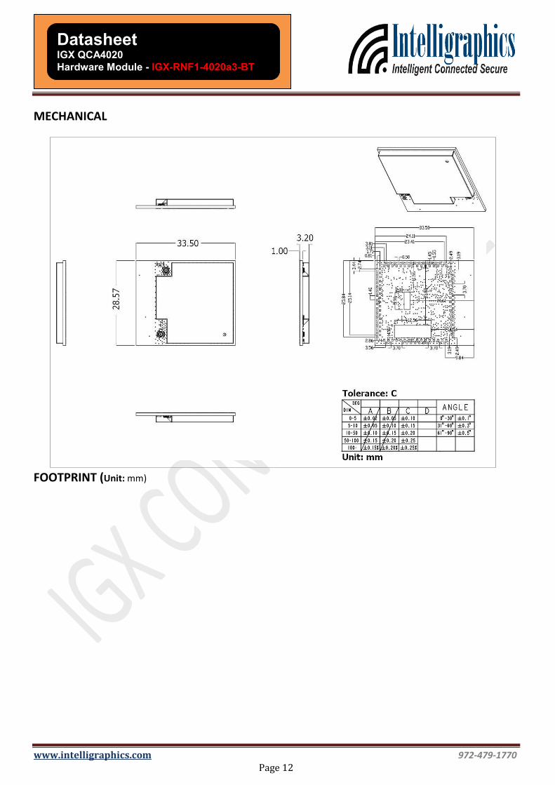
MECHANICAL
FOOTPRINT (Unit: mm)

www.intelligraphics.com 972-479-1770
Page 13
Datasheet IGX QCA4020
Hardware Module - IGX-RNF1-4020a3-BT
www.intelligraphics.com 972-479-1770
Page 14
Datasheet IGX QCA4020
Hardware Module - IGX-RNF1-4020a3-BT
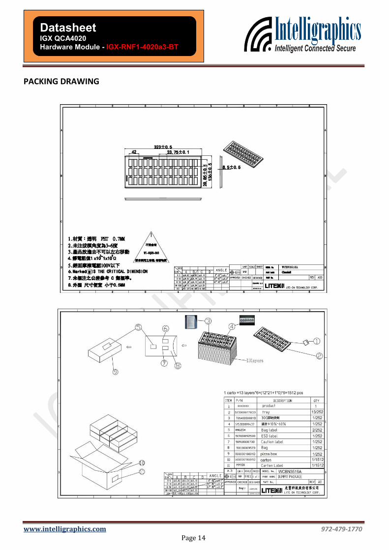
PACKING DRAWING
www.intelligraphics.com 972-479-1770
Page 15
Datasheet IGX QCA4020
Hardware Module - IGX-RNF1-4020a3-BT
ENVIRONMENTAL
OPERATING
Ambient Operating Temperature: -20 to 80C
Relative Humidity: 5-90% (non-condensing)
STORAGE
Temperature: -40 to 80C (-40 to 176F)
Relative Humidity: 5-95% (non-condensing)