Embed Size (px)
Citation preview
X+/-
D
EN
>> 17
A[17:0]
B[17:0]
SN-1[43:0]
C[43:0]
SHIFT17
SEL_CASC
SN[43:0]
OVFL
ADD_SUB
0
LUT4A
B
C
D
LUT_BYPEN
CLKRST
LO
RO
CIN
CO
D
EN
SL
SYNC_SR
IGLOO®2 FPGAs
Up to 150K LEs | DSP | SERDES | PCIe Gen2 | XAUI | I/O Density
More Resources in Low-Density Devices
Lowest Power
Proven Security
Exceptional Reliability
2
More Resources in Low-Density Devices • PCIe Gen2 support in 10K LE • High-performance memory subsystem • Highest I/O density
With Clear Advantages• Lowest Power
• Reduces total power by up to 50% • 70 mW per 5G SERDES (PCIe Gen2)
• Proven Security • Protection from overbuilding and cloning• Secure boot for FPGA and processors
• Exceptional Reliability • SEU immune zero FIT flash FPGA configuration• Reliable safety-critical and mission-critical systems
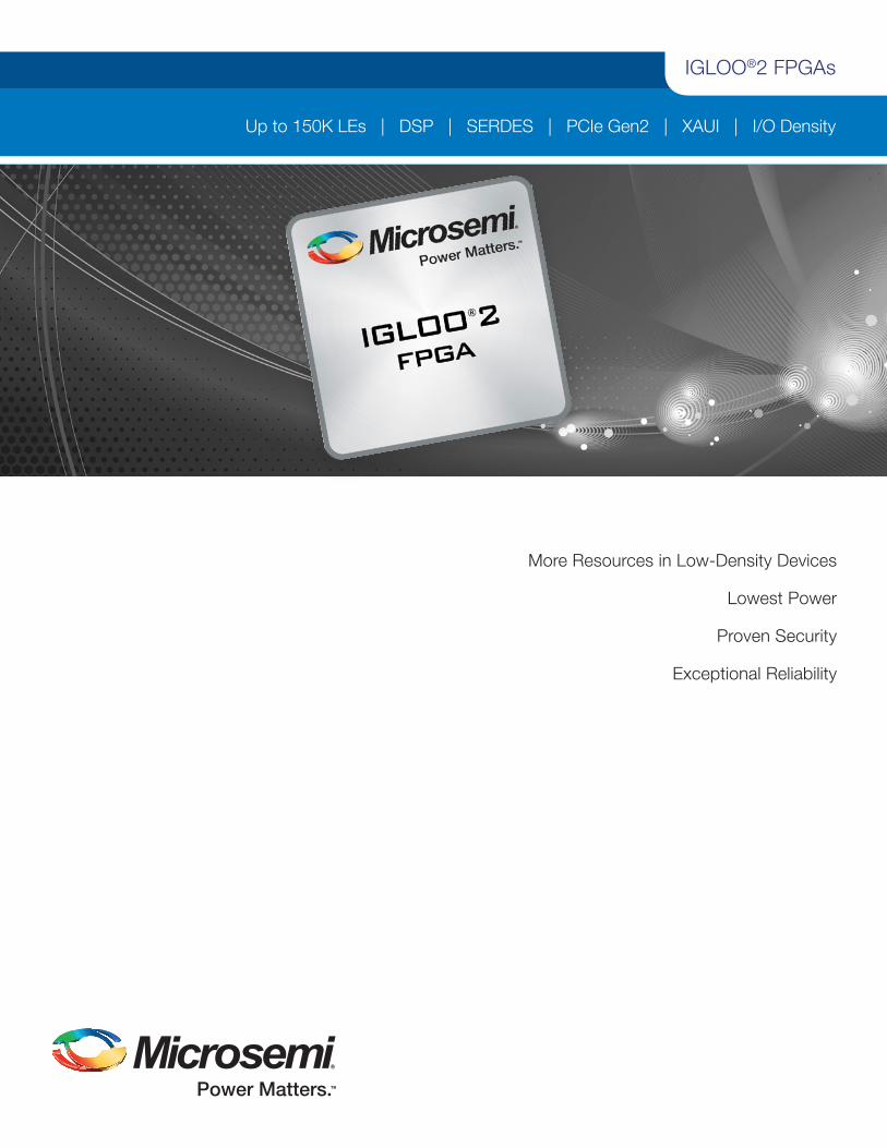
IGLOO2 Advantages
IGLOO2 FPGAs
Communications Industrial Defense Automotive
IGLOO2 FPGAs are ideal for general purpose functions such as Gigabit Ethernet or dual-PCI Express control planes, bridging functions, input/output (I/O) expansion and conversion, video/image processing, system management, and secure connectivity. Microsemi FPGAs are used by customers in communications, industrial, medical, defense, and aviation markets.
Microsemi IGLOO2 FPGAs Offer More Resources in Low-Density Devices with the Lowest Power, Proven Security, and Exceptional Reliability

3
PCI Express DDR3 Controller Secure Flash
IGLOO2 FPGAs offer 5K–150K LEs with a high-performance memory subsystem, up to 512 KB embedded flash, 2 × 32 KB embedded static random-access memory (SRAM), two direct memory access (DMA) engines, and two double data rate (DDR) memory controllers. Architecture highlights include the following:
• Up to 16× transceiver lanes
• PCIe Gen2, XAUI/XGXS+, generic ePCS mode at 3.2G
• Up to 150K LEs, 5 Mbit SRAM, 4 Mbit eNVM
• Hard 667 Mbps DDR2/3 controllers
• Integrated DSP processing blocks
• Power as low as 7 mW standby, typical
• DPA-hardened, AES256, SHA256, on-demand NVM data
integrity check
• SEU-protected/tolerant memories: eSRAMs, DDR bridges
IGLOO2 FPGA Architecture
AES Advanced Encryption Standard FIC Fabric Interface Controller
AHB Advanced High-Performance Bus HPMS High Performance Memory Subsystem
APB Advanced Peripheral Bus SHA Secure Hashing Algorithm
AXI Advanced eXtensible Interface XAUI 10 Gbps Attachment Unit Interface
DDR Double Data Rate XGMII 10 Gigabit Media Independent Interface
ECC Elliptical Curve Cryptography XGXS XGMII Extended Sublayer
PCI Expressx1, x2, x4
PMA PMA PMA PMA
XAUIXGXS
AXI/AHB, XGMII, Direct 20 Bit Bus
Up to 16 Lanes Multi Protocol SERDES
FPGA FabricUp to 150K Logic Elements
SystemController
Direct Attachx1, x2, x4
Large SRAM (1024x18)
Micro SRAM(64x18)
11–240 10–23611–240
Math Blocks (18x18)AES256 SHA256
ECC
SRAM – PUF
NRBG
Math Blocks (18x18)
Micro SRAM(64x18)
Multi-Standard GPIO(1.2 V–3.3 V, LVDS, HSTL/SSTL)
Large SRAM(1024x18)
IGLOO®2 FPGA
Standard Cell/SEU Immune
FlashBased/SEU Immune
FIC
AXI/AHB
DDR Bridge
667 Mbps DDRController/PHY
667 Mbps DDRController/PHY
AXI/AHB
AH
B B
us M
atrix
High Performance Memory Subsystem
COMM_BLK
SPI
eNVM
eSRAM_0
eSRAM_1
PDMA
HPDMA
FIC

4
General Purpose Applications
PCIe 1G Control Plane• PCIe Gen2 in 10K LE devices
with I/O expansion
Multi-Axis Motor Control• Deterministic and secure multi-axis/
high-RPM solutions• Motor control IP and development kit
Audio Processing, Storage, and Retrieval• I2S-to-SPI bridge allows multiple audio recordings and playbacks
IGLOO2 FPGA
System ControlPWM Timing
PID ControlLoop
Transforms
Host Interface
eNVM,eSRAM
PowerManagement
Timing
AutomationController/Host CPU
Inverter Bridge,IGBTs,
SiC MOSFETS
PowerSupply/
Conversion
Sensors:Speed, Torque,
Position A/DConversion
IGLOO2 FPGA
Conversion,Buffering &Formatter
Host Interface
I2SInterface
SPIInterfaceTimberwolf
ZL38051Audio Processor
2 DigitalMEMS
Microphones
Audio Jack
SPI Flash
Peripherals
Flash,SRAM
CPU
MCU
GigabitEthernet PHY
SERDES
Security
FPGAFabric
IGLOO2 FPGA
HighPerformance
MemorySubsystem
10/100Ethernet PHY
DDR3DRAM
LCD
I2CGPIO
SPI
SPI
USB
PCIe
DDR3DRAM
SPI FLASH

5
General Purpose Applications
Bridging and Co-Processing• SERDES to bridge CPRI, ADC/DAC
Secure Connectivity• Best-in-class security data communications and anti-tamper• Ultra-low static power for portability
DDC
BasebandProcessing
Crypto
DCU
ReceiverADC
TransmitterDAC
Antenna MemorySubsystem
DataProcessing
RFFrontEnd
IGLOO2 FPGA
Board Initialization• PMBus, instant-on
OOO
HostProcessor PoE
Managers
eSPII2C
PMBus
StatusLEDs
SGMII
SGMII
SGMII
SGMII
SGMII
RJ45/SFP
RJ45/SFP
RJ45/SFP
5 V PoLSupply
PMBusInterface
eSPIController
I2CController
SystemControl
EthernetSwitch
PoEPD69208
PoEPD69208
EthernetPHY
EthernetPHY
EthernetPHY
PoEPD69208
ClockManagement
IGLOO2 FPGA
3.3 V PoLSupply
2.5 V PoLSupply
1.5 V PoLSupply
IGLOO2 FPGA
CPRI JESD204BCPRIDFE
Co-ProcessingMemory
SubsystemADC/DACInterfacing
6
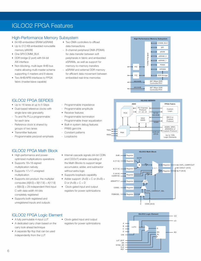
High-Performance Memory Subsystem• 64 KB embedded SRAM (eSRAM)
• Up to 512 KB embedded nonvolatile
memory (eNVM)
• One SPI/COMM_BLK
• DDR bridge (2 port) with 64-bit
AXI interface
• Non-blocking, multi-layer AHB bus
matrix allowing multi-master scheme
supporting 4 masters and 8 slaves
• Two AHB/APB interfaces to FPGA
fabric (master/slave capable)
• Two DMA controllers to offload
data transactions
- 8-channel peripheral DMA (PDMA)
for data transfer between soft
peripherals in fabric and embedded
eSRAMs, as well as support for
memory-to-memory transfers
- eSRAM and external DDR memory
for efficient data movement between
embedded real-time memories FIC
AXI/AHB
DDR Bridge
667 Mbps DDRController/PHY
667 Mbps DDRController/PHY
AXI/AHB
AH
B B
us M
atrix
High Performance Memory Subsystem
COMM_BLK
SPI
eNVM
eSRAM_0
eSRAM_1
PDMA
HPDMAFIC
IGLOO2 FPGA SERDES• Up to 16 lanes at up to 5 Gbps
• Dual-based reference clocks with
single-lane rate granularity
- Tx and Rx PLLs programmable
for each lane
- Reference clock is shared by
groups of two lanes
• Transmitter features
- Programmable pre/post-emphasis
- Programmable impedance
- Programmable amplitude
• Receiver features
- Programmable termination
- Programmable linear equalization
• Built-in system debug features
- PRBS gen/chk
- Constant patterns
- Loopbacks
IGLOO2 SERDES
FPGA FabricASIC
Up to 150kLogic Elements
PCI ExpressProtocol
x1, x2, x4
XAUIXGXS
CustomLogic
802.3 orCustomProtocol
SGMII, SRIO,JESD204x or
Custom ProtocolPMA
64-bitAXI/AHB
4x20-bitEPCS
XGMII
TXDn
RXDn
PCS
IGLOO2 FPGA Math Block• High-performance and power-
optimized multiplications operations
• Supports 18×18-signed
multiplication natively
• Supports 17×17-unsigned
multiplication
• Supports dot product: the multiplier
computes (A[8:0] × B[17:9] + A[17:9]
× B[8:0]) × 29 independent third input
C with data width 44-bits
completely registered
• Supports both registered and
unregistered inputs and outputs
• Internal cascade signals (44-bit CDIN
and CDOUT) enable cascading of
the Math Blocks to support larger
accumulator, adder, and subtractor
without extra logic
• Supports loopback capability
• Adder support: (A×B) + C or (A×B) +
D or (A×B) + C + D
• Clock-gated input and output
registers for power optimizations
RegisterSUB
A [17:0]
B [17:0]
C [43:0]
Register
Register
Register
Register
Register
Register
Register OVFL_CARRYOUT
CDOUT [43:0]
P [46:0]
+ / –
CARRYIN
ARSHFT17
CDSEL
FDBKSEL
OVFL_CARROUT_SEL
DOTP
36
44
44
0 CDIN [43:0]
>>17
Register
IGLOO2 Math Block
IGLOO2 FPGA Logic Element • A fully permutable 4-input LUT
• A dedicated carry chain based on the
carry look-ahead technique
• A separate flip-flop that can be used
independently from the LUT
• Clock-gated input and output
registers for power optimizations A
B
C
D
CIN
LUT_BYPEN
SYNC_SRCLKRST
D
EN
CO
LO
ROSL
LUT4
IGLOO2 Logic Element
IGLOO2 FPGA Features
7
Design Resources
Intellectual PropertyMicrosemi enhances your design productivity by providing an extensive suite of proven and optimized IP cores for use with Microsemi FPGAs. Our extensive suite of IP cores covers all key markets and applications. Our cores are organized as either Microsemi-developed DirectCores or third-party-developed CompanionCores. Most DirectCores are available for free within our Libero tool suite and include common communications interfaces, peripherals, and processing elements.
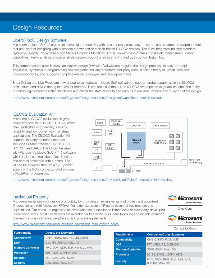
IGLOO2 Evaluation KitMicrosemi’s IGLOO2 evaluation kit gives designers access to IGLOO2 FPGAs, which offer leadership in I/O density, security, reliability, and low power into mainstream applications. The IGLOO2 Evaluation Kit supports industry-standard interfaces, including Gigabit Ethernet, USB 2.0 OTG, SPI, I2C, and UART. The kit can be used with Microsemi’s Libero SoC v11.5 software, which includes a free Libero Gold license, and comes preloaded with a demo. The kit can be powered through a 12 V power supply or the PCIe connector, and includes a FlashPro4 programmer.
http://www.microsemi.com/products/fpga-soc/design-resources/dev-kits/igloo2/igloo2-evaluation-kit#overview
USB-OTG
USB-UART
I2C
RJ45
LEDs FP4/IARHeader
LPDDR GPIO Header
12 V fromWall Supply
x1 PCIe
FR4 PCB Material
Tx/Rx/ClkSMA Pairs
GbEPHY
SPIFlash
IGLOO2FPGA
Functionality DirectCore Examples
Connectivity UART,16550, 429, PCI, JESD204B
DSP CIC, FFT ,FIR, CORDIC, RS
Memory Controller FIFO, DDR, QDR, SDR, MemCtrl, MMC
Processor 8051, 8051s, ARM7TDMI
Ethernet MII, RGMII, GMII, SGMII
Security DES, 3DES, AES, SHA
Functionality CompanionCores Examples
Connectivity CAN, CANFD, PCIE, VME
DSP FFT, JPEG, RS, DVBMOD
Memory Controller SDRAMDDR, Flash, SD
Processor 80188, 80186, LEON3, 6809
SecurityMD5, ARC4, RNG, ZUC, AES, SHA, 802.1ae (MACSec)
DirectCore™
CompanionCore™
http://www.microsemi.com/products/fpga-soc/design-resources/design-software/libero-soc#downloads
http://www.microsemi.com/products/fpga-soc/design-resources/ip-cores
Libero® SoC Design SoftwareMicrosemi’s Libero SoC design suite offers high productivity with its comprehensive, easy-to-learn, easy-to-adopt development tools that are used for designing with Microsemi’s power efficient flash-based IGLOO2 devices. The suite integrates industry standard Synopsys Synplify Pro synthesis and Mentor Graphics ModelSim simulation with best-in-class constraints management, debug capabilities, timing analysis, power analysis, secure production programming and push button design flow.
This comprehensive suite features an intuitive design flow with GUI wizards to guide the design process. Its easy-to-adopt single-click synthesis to programming flow integrates industry-standard third-party tools, a rich IP library of DirectCores and CompanionCores, and supports complete reference designs and development kits.
SmartDebug and Live Probe are new debug tools available in Libero SoC software to support probe capabilities in the IGLOO2 architecture and device debug features for memory. These tools use the built-in IGLOO2 probe points to greatly enhance the ability to debug logic elements within the device and check the state of inputs and outputs in real time, without any re-layout of the design.

©2016 Microsemi Corporation. All rights reserved. Microsemi and the Microsemi logo are registered trademarks of Microsemi Corporation. All other trademarks and service marks are the property of their respective owners.
Microsemi makes no warranty, representation, or guarantee regarding the information contained herein or the suitability of its products and services for any particular purpose, nor does Microsemi assume any liability whatsoever arising out of the application or use of any product or circuit. The products sold hereunder and any other products sold by Microsemi have been subject to limited testing and should not be used in conjunction with mission-critical equipment or applications. Any performance specifications are believed to be reliable but are not verified, and Buyer must conduct and complete all performance and other testing of the products, alone and together with, or installed in, any end-products. Buyer shall not rely on any data and performance specifications or parameters provided by Microsemi. It is the Buyer’s responsibility to independently determine suitability of any products and to test and verify the same. The information provided by Microsemi hereunder is provided “as is, where is” and with all faults, and the entire risk associated with such information is entirely with the Buyer. Microsemi does not grant, explicitly or implicitly, to any party any patent rights, licenses, or any other IP rights, whether with regard to such information itself or anything described by such information. Information provided in this document is proprietary to Microsemi, and Microsemi reserves the right to make any changes to the information in this document or to any products and services at any time without notice.
Microsemi Corporation (Nasdaq: MSCC) offers a comprehensive portfolio of semiconductor and system solutions for aerospace & defense, communications, data center and industrial markets. Products include high-performance and radiation-hardened analog mixed-signal integrated circuits, FPGAs, SoCs and ASICs; power management products; timing and synchronization devices and precise time solutions, setting the world’s standard for time; voice processing devices; RF solutions; discrete components; enterprise storage and communication solutions, security technologies and scalable anti-tamper products; Ethernet solutions; Power-over-Ethernet ICs and midspans; as well as custom design capabilities and services. Microsemi is headquartered in Aliso Viejo, California and has approximately 4,800 employees globally. Learn more at www.microsemi.com.
Microsemi Corporate HeadquartersOne Enterprise, Aliso Viejo, CA 92656 USAWithin the USA: +1 (800) 713-4113 Outside the USA: +1 (949) 380-6100 Fax: +1 (949) 215-4996Email: [email protected] www.microsemi.com
IGLOO2 Devices Features M2GL005 M2GL010 M2GL025 M2GL050 M2GL060 M2GL090 M2GL150
Logic/DSP
Maximum Logic Elements (4LUT + DFF) 6,060 12,084 27,696 56,340 56,520 86,184 146,124
Math Blocks (18x18) 11 22 34 72 72 84 240
PLLs and CCCs 2 6 8
SPI/HPDMA/PDMA 1 each
Fabric Interface Controllers (FICs) 1 2 1 2
Data Security AES256, SHA256, RNG AES256, SHA256, RNG, ECC, PUF
Memory
eNVM (K Bytes) 128 256 512
LSRAM 18 K Blocks 10 21 31 69 109 236
uSRAM 1 K Blocks 11 21 34 72 112 240
eSRAM (K Bytes) 64
Total RAM (K bits) 703 912 1104 1826 2586 5000
High Speed
DDR Controllers (count × width) 1×18 2×36 1×18 2x36
SERDES Lanes 0 4 8 4 16
PCIe End Points 0 1 2 4
User I/O
MSIO (3.3V) 115 123 157 139 271 309 292
MSIOD (2.5V) 28 40 62 40 106
DDRIO (2.5V) 66 70 176 76 176
Total User I/Os 209 233 267 377 387 425 574
Grades Commercial (C), Industrial (I), Military (M) C, I C, I, M
Note:* Total logic may vary based on utilization of DSP and memories in your design. Please see the IGLOO2 Fabric UG for details.* Feature availablility is package dependent
I/Os Per PackagePackage Options
Package Type FCS(G)325 VF(G)256 FCS(G)536 VF(G)400 FCV(G)484 TQ(G)144 FG(G)484 FG(G)676 FG(G)896 FC(G)1152
Pitch (mm) 0.5 0.8 0.5 0.8 0.5 1.0 1.0 1.0 1.0
Length x Width (mm) 11x11 14x14 16x16 17x17 19x19 20x20 23x23 27x27 31x31 35x35
Device I/O Lanes I/O Lanes I/O Lanes I/O Lanes I/O Lanes I/O Lanes I/O Lanes I/O Lanes I/O Lanes I/O Lanes
M2GL005 (S) — — 161 — — — 171 — — — 84 — 209 — — — — — — —
M2GL010 (S/T/TS) — — 138 2 — — 195 4 — — 84 — 233 4 — — — — — —
M2GL025 (T/TS) 180 2 138 2 — — 207 4 — — — — 267 4 — — — — — —
M2GL050 (T/TS) 200 2 — — — — 207 4 — — — — 267 4 — — 377 8 — —
M2GL060 (T/TS) 200 2 — — — — 207 4 — — — — 267 4 387 4 — — — —
M2GL090 (T/TS) 180 4 — — — — — — — — — — 267 4 425 4 — — — —
M2GL150 (T/TS) — — — — 293 4 — — 248 4 — — — — — — — — 574 16
Note: M2GL090 FCS325 is 11x13.5 pkg dim Highlighted devices can migrate vertically in the same package
IGLOO2 FPGA Product Family
IGLOO2-10/16